JPWO2012144249A1 - Power conversion device and in-vehicle power supply device including the same - Google Patents
Power conversion device and in-vehicle power supply device including the same Download PDFInfo
- Publication number
- JPWO2012144249A1 JPWO2012144249A1 JP2013510905A JP2013510905A JPWO2012144249A1 JP WO2012144249 A1 JPWO2012144249 A1 JP WO2012144249A1 JP 2013510905 A JP2013510905 A JP 2013510905A JP 2013510905 A JP2013510905 A JP 2013510905A JP WO2012144249 A1 JPWO2012144249 A1 JP WO2012144249A1
- Authority
- JP
- Japan
- Prior art keywords
- inverter unit
- voltage
- power
- circuit
- semiconductor switching
- Prior art date
- Legal status (The legal status is an assumption and is not a legal conclusion. Google has not performed a legal analysis and makes no representation as to the accuracy of the status listed.)
- Granted
Links
Images


Classifications
-
- B—PERFORMING OPERATIONS; TRANSPORTING
- B60—VEHICLES IN GENERAL
- B60L—PROPULSION OF ELECTRICALLY-PROPELLED VEHICLES; SUPPLYING ELECTRIC POWER FOR AUXILIARY EQUIPMENT OF ELECTRICALLY-PROPELLED VEHICLES; ELECTRODYNAMIC BRAKE SYSTEMS FOR VEHICLES IN GENERAL; MAGNETIC SUSPENSION OR LEVITATION FOR VEHICLES; MONITORING OPERATING VARIABLES OF ELECTRICALLY-PROPELLED VEHICLES; ELECTRIC SAFETY DEVICES FOR ELECTRICALLY-PROPELLED VEHICLES
- B60L53/00—Methods of charging batteries, specially adapted for electric vehicles; Charging stations or on-board charging equipment therefor; Exchange of energy storage elements in electric vehicles
- B60L53/20—Methods of charging batteries, specially adapted for electric vehicles; Charging stations or on-board charging equipment therefor; Exchange of energy storage elements in electric vehicles characterised by converters located in the vehicle
- B60L53/22—Constructional details or arrangements of charging converters specially adapted for charging electric vehicles
-
- H—ELECTRICITY
- H02—GENERATION; CONVERSION OR DISTRIBUTION OF ELECTRIC POWER
- H02M—APPARATUS FOR CONVERSION BETWEEN AC AND AC, BETWEEN AC AND DC, OR BETWEEN DC AND DC, AND FOR USE WITH MAINS OR SIMILAR POWER SUPPLY SYSTEMS; CONVERSION OF DC OR AC INPUT POWER INTO SURGE OUTPUT POWER; CONTROL OR REGULATION THEREOF
- H02M3/00—Conversion of dc power input into dc power output
- H02M3/22—Conversion of dc power input into dc power output with intermediate conversion into ac
- H02M3/24—Conversion of dc power input into dc power output with intermediate conversion into ac by static converters
- H02M3/28—Conversion of dc power input into dc power output with intermediate conversion into ac by static converters using discharge tubes with control electrode or semiconductor devices with control electrode to produce the intermediate ac
- H02M3/325—Conversion of dc power input into dc power output with intermediate conversion into ac by static converters using discharge tubes with control electrode or semiconductor devices with control electrode to produce the intermediate ac using devices of a triode or a transistor type requiring continuous application of a control signal
- H02M3/335—Conversion of dc power input into dc power output with intermediate conversion into ac by static converters using discharge tubes with control electrode or semiconductor devices with control electrode to produce the intermediate ac using devices of a triode or a transistor type requiring continuous application of a control signal using semiconductor devices only
- H02M3/33507—Conversion of dc power input into dc power output with intermediate conversion into ac by static converters using discharge tubes with control electrode or semiconductor devices with control electrode to produce the intermediate ac using devices of a triode or a transistor type requiring continuous application of a control signal using semiconductor devices only with automatic control of the output voltage or current, e.g. flyback converters
-
- H—ELECTRICITY
- H02—GENERATION; CONVERSION OR DISTRIBUTION OF ELECTRIC POWER
- H02M—APPARATUS FOR CONVERSION BETWEEN AC AND AC, BETWEEN AC AND DC, OR BETWEEN DC AND DC, AND FOR USE WITH MAINS OR SIMILAR POWER SUPPLY SYSTEMS; CONVERSION OF DC OR AC INPUT POWER INTO SURGE OUTPUT POWER; CONTROL OR REGULATION THEREOF
- H02M1/00—Details of apparatus for conversion
- H02M1/38—Means for preventing simultaneous conduction of switches
-
- H—ELECTRICITY
- H02—GENERATION; CONVERSION OR DISTRIBUTION OF ELECTRIC POWER
- H02M—APPARATUS FOR CONVERSION BETWEEN AC AND AC, BETWEEN AC AND DC, OR BETWEEN DC AND DC, AND FOR USE WITH MAINS OR SIMILAR POWER SUPPLY SYSTEMS; CONVERSION OF DC OR AC INPUT POWER INTO SURGE OUTPUT POWER; CONTROL OR REGULATION THEREOF
- H02M3/00—Conversion of dc power input into dc power output
- H02M3/22—Conversion of dc power input into dc power output with intermediate conversion into ac
- H02M3/24—Conversion of dc power input into dc power output with intermediate conversion into ac by static converters
- H02M3/28—Conversion of dc power input into dc power output with intermediate conversion into ac by static converters using discharge tubes with control electrode or semiconductor devices with control electrode to produce the intermediate ac
- H02M3/325—Conversion of dc power input into dc power output with intermediate conversion into ac by static converters using discharge tubes with control electrode or semiconductor devices with control electrode to produce the intermediate ac using devices of a triode or a transistor type requiring continuous application of a control signal
- H02M3/335—Conversion of dc power input into dc power output with intermediate conversion into ac by static converters using discharge tubes with control electrode or semiconductor devices with control electrode to produce the intermediate ac using devices of a triode or a transistor type requiring continuous application of a control signal using semiconductor devices only
- H02M3/337—Conversion of dc power input into dc power output with intermediate conversion into ac by static converters using discharge tubes with control electrode or semiconductor devices with control electrode to produce the intermediate ac using devices of a triode or a transistor type requiring continuous application of a control signal using semiconductor devices only in push-pull configuration
- H02M3/3376—Conversion of dc power input into dc power output with intermediate conversion into ac by static converters using discharge tubes with control electrode or semiconductor devices with control electrode to produce the intermediate ac using devices of a triode or a transistor type requiring continuous application of a control signal using semiconductor devices only in push-pull configuration with automatic control of output voltage or current
-
- B—PERFORMING OPERATIONS; TRANSPORTING
- B60—VEHICLES IN GENERAL
- B60L—PROPULSION OF ELECTRICALLY-PROPELLED VEHICLES; SUPPLYING ELECTRIC POWER FOR AUXILIARY EQUIPMENT OF ELECTRICALLY-PROPELLED VEHICLES; ELECTRODYNAMIC BRAKE SYSTEMS FOR VEHICLES IN GENERAL; MAGNETIC SUSPENSION OR LEVITATION FOR VEHICLES; MONITORING OPERATING VARIABLES OF ELECTRICALLY-PROPELLED VEHICLES; ELECTRIC SAFETY DEVICES FOR ELECTRICALLY-PROPELLED VEHICLES
- B60L2210/00—Converter types
- B60L2210/10—DC to DC converters
-
- B—PERFORMING OPERATIONS; TRANSPORTING
- B60—VEHICLES IN GENERAL
- B60L—PROPULSION OF ELECTRICALLY-PROPELLED VEHICLES; SUPPLYING ELECTRIC POWER FOR AUXILIARY EQUIPMENT OF ELECTRICALLY-PROPELLED VEHICLES; ELECTRODYNAMIC BRAKE SYSTEMS FOR VEHICLES IN GENERAL; MAGNETIC SUSPENSION OR LEVITATION FOR VEHICLES; MONITORING OPERATING VARIABLES OF ELECTRICALLY-PROPELLED VEHICLES; ELECTRIC SAFETY DEVICES FOR ELECTRICALLY-PROPELLED VEHICLES
- B60L2210/00—Converter types
- B60L2210/30—AC to DC converters
-
- B—PERFORMING OPERATIONS; TRANSPORTING
- B60—VEHICLES IN GENERAL
- B60L—PROPULSION OF ELECTRICALLY-PROPELLED VEHICLES; SUPPLYING ELECTRIC POWER FOR AUXILIARY EQUIPMENT OF ELECTRICALLY-PROPELLED VEHICLES; ELECTRODYNAMIC BRAKE SYSTEMS FOR VEHICLES IN GENERAL; MAGNETIC SUSPENSION OR LEVITATION FOR VEHICLES; MONITORING OPERATING VARIABLES OF ELECTRICALLY-PROPELLED VEHICLES; ELECTRIC SAFETY DEVICES FOR ELECTRICALLY-PROPELLED VEHICLES
- B60L2210/00—Converter types
- B60L2210/40—DC to AC converters
-
- H—ELECTRICITY
- H02—GENERATION; CONVERSION OR DISTRIBUTION OF ELECTRIC POWER
- H02M—APPARATUS FOR CONVERSION BETWEEN AC AND AC, BETWEEN AC AND DC, OR BETWEEN DC AND DC, AND FOR USE WITH MAINS OR SIMILAR POWER SUPPLY SYSTEMS; CONVERSION OF DC OR AC INPUT POWER INTO SURGE OUTPUT POWER; CONTROL OR REGULATION THEREOF
- H02M1/00—Details of apparatus for conversion
- H02M1/0003—Details of control, feedback or regulation circuits
- H02M1/0032—Control circuits allowing low power mode operation, e.g. in standby mode
-
- H—ELECTRICITY
- H02—GENERATION; CONVERSION OR DISTRIBUTION OF ELECTRIC POWER
- H02M—APPARATUS FOR CONVERSION BETWEEN AC AND AC, BETWEEN AC AND DC, OR BETWEEN DC AND DC, AND FOR USE WITH MAINS OR SIMILAR POWER SUPPLY SYSTEMS; CONVERSION OF DC OR AC INPUT POWER INTO SURGE OUTPUT POWER; CONTROL OR REGULATION THEREOF
- H02M1/00—Details of apparatus for conversion
- H02M1/0048—Circuits or arrangements for reducing losses
- H02M1/0054—Transistor switching losses
- H02M1/0058—Transistor switching losses by employing soft switching techniques, i.e. commutation of transistors when applied voltage is zero or when current flow is zero
-
- Y—GENERAL TAGGING OF NEW TECHNOLOGICAL DEVELOPMENTS; GENERAL TAGGING OF CROSS-SECTIONAL TECHNOLOGIES SPANNING OVER SEVERAL SECTIONS OF THE IPC; TECHNICAL SUBJECTS COVERED BY FORMER USPC CROSS-REFERENCE ART COLLECTIONS [XRACs] AND DIGESTS
- Y02—TECHNOLOGIES OR APPLICATIONS FOR MITIGATION OR ADAPTATION AGAINST CLIMATE CHANGE
- Y02T—CLIMATE CHANGE MITIGATION TECHNOLOGIES RELATED TO TRANSPORTATION
- Y02T10/00—Road transport of goods or passengers
- Y02T10/60—Other road transportation technologies with climate change mitigation effect
- Y02T10/70—Energy storage systems for electromobility, e.g. batteries
-
- Y—GENERAL TAGGING OF NEW TECHNOLOGICAL DEVELOPMENTS; GENERAL TAGGING OF CROSS-SECTIONAL TECHNOLOGIES SPANNING OVER SEVERAL SECTIONS OF THE IPC; TECHNICAL SUBJECTS COVERED BY FORMER USPC CROSS-REFERENCE ART COLLECTIONS [XRACs] AND DIGESTS
- Y02—TECHNOLOGIES OR APPLICATIONS FOR MITIGATION OR ADAPTATION AGAINST CLIMATE CHANGE
- Y02T—CLIMATE CHANGE MITIGATION TECHNOLOGIES RELATED TO TRANSPORTATION
- Y02T10/00—Road transport of goods or passengers
- Y02T10/60—Other road transportation technologies with climate change mitigation effect
- Y02T10/7072—Electromobility specific charging systems or methods for batteries, ultracapacitors, supercapacitors or double-layer capacitors
-
- Y—GENERAL TAGGING OF NEW TECHNOLOGICAL DEVELOPMENTS; GENERAL TAGGING OF CROSS-SECTIONAL TECHNOLOGIES SPANNING OVER SEVERAL SECTIONS OF THE IPC; TECHNICAL SUBJECTS COVERED BY FORMER USPC CROSS-REFERENCE ART COLLECTIONS [XRACs] AND DIGESTS
- Y02—TECHNOLOGIES OR APPLICATIONS FOR MITIGATION OR ADAPTATION AGAINST CLIMATE CHANGE
- Y02T—CLIMATE CHANGE MITIGATION TECHNOLOGIES RELATED TO TRANSPORTATION
- Y02T10/00—Road transport of goods or passengers
- Y02T10/60—Other road transportation technologies with climate change mitigation effect
- Y02T10/72—Electric energy management in electromobility
-
- Y—GENERAL TAGGING OF NEW TECHNOLOGICAL DEVELOPMENTS; GENERAL TAGGING OF CROSS-SECTIONAL TECHNOLOGIES SPANNING OVER SEVERAL SECTIONS OF THE IPC; TECHNICAL SUBJECTS COVERED BY FORMER USPC CROSS-REFERENCE ART COLLECTIONS [XRACs] AND DIGESTS
- Y02—TECHNOLOGIES OR APPLICATIONS FOR MITIGATION OR ADAPTATION AGAINST CLIMATE CHANGE
- Y02T—CLIMATE CHANGE MITIGATION TECHNOLOGIES RELATED TO TRANSPORTATION
- Y02T10/00—Road transport of goods or passengers
- Y02T10/80—Technologies aiming to reduce greenhouse gasses emissions common to all road transportation technologies
- Y02T10/92—Energy efficient charging or discharging systems for batteries, ultracapacitors, supercapacitors or double-layer capacitors specially adapted for vehicles
-
- Y—GENERAL TAGGING OF NEW TECHNOLOGICAL DEVELOPMENTS; GENERAL TAGGING OF CROSS-SECTIONAL TECHNOLOGIES SPANNING OVER SEVERAL SECTIONS OF THE IPC; TECHNICAL SUBJECTS COVERED BY FORMER USPC CROSS-REFERENCE ART COLLECTIONS [XRACs] AND DIGESTS
- Y02—TECHNOLOGIES OR APPLICATIONS FOR MITIGATION OR ADAPTATION AGAINST CLIMATE CHANGE
- Y02T—CLIMATE CHANGE MITIGATION TECHNOLOGIES RELATED TO TRANSPORTATION
- Y02T90/00—Enabling technologies or technologies with a potential or indirect contribution to GHG emissions mitigation
- Y02T90/10—Technologies relating to charging of electric vehicles
- Y02T90/12—Electric charging stations
-
- Y—GENERAL TAGGING OF NEW TECHNOLOGICAL DEVELOPMENTS; GENERAL TAGGING OF CROSS-SECTIONAL TECHNOLOGIES SPANNING OVER SEVERAL SECTIONS OF THE IPC; TECHNICAL SUBJECTS COVERED BY FORMER USPC CROSS-REFERENCE ART COLLECTIONS [XRACs] AND DIGESTS
- Y02—TECHNOLOGIES OR APPLICATIONS FOR MITIGATION OR ADAPTATION AGAINST CLIMATE CHANGE
- Y02T—CLIMATE CHANGE MITIGATION TECHNOLOGIES RELATED TO TRANSPORTATION
- Y02T90/00—Enabling technologies or technologies with a potential or indirect contribution to GHG emissions mitigation
- Y02T90/10—Technologies relating to charging of electric vehicles
- Y02T90/14—Plug-in electric vehicles
Abstract
ゼロ電圧スイッチングを行うDC/DCコンバータにおいて、トランス(8)の一次側のインバータ部(15)内の第1、第2のMOSFET(5a、5b)にコンデンサ(6a、6b)が並列接続され、交流出力線にインダクタ(7)が接続される。制御回路(30)は、電流(i)が所定値を超える領域で、デッドタイム(td)固定のPWM制御を用いてインバータ部(15)を制御し、電流(i)が所定値以下になる軽負荷領域では、PFM制御に切り換え、電流(i)の減少に伴ってデッドタイム(td)が長くなるように周波数を低減させてデューティ比を変化させずに保持する。In the DC / DC converter that performs zero voltage switching, capacitors (6a, 6b) are connected in parallel to the first and second MOSFETs (5a, 5b) in the primary inverter section (15) of the transformer (8), An inductor (7) is connected to the AC output line. The control circuit (30) controls the inverter unit (15) using PWM control with a fixed dead time (td) in a region where the current (i) exceeds a predetermined value, and the current (i) becomes equal to or less than the predetermined value. In the light load region, switching to PFM control is performed and the frequency is reduced so that the dead time (td) becomes longer as the current (i) decreases, and the duty ratio is kept unchanged.
Description
この発明は、直流電力を異なる電圧の直流電力に変換して出力する電力変換装置、およびそれを備えた車載電源装置に関するものである。 The present invention relates to a power conversion device that converts DC power into DC power of a different voltage and outputs the power, and an in-vehicle power supply device including the same.
自動車の二酸化炭素排出量の削減を目指して、エネルギ利用効率を高めるよう燃費向上が強く求められている。近年、従来のエンジンのみで走行する従来自動車に加えて、エンジンとモータジェネレータを組み合わせたハイブリッド自動車や、モータのみで走行する電気自動車などの電動車両が登場し電動車両の普及が急速に進んできている。電動車両においては、従来の鉛バッテリである低圧バッテリに加えて、モータジェネレータにエネルギ供給を行うためにニッケル水素バッテリやリチウムイオンバッテリなどの高圧バッテリが用いられている。
電動車両においては発電機(オルタネータ)がなく、代わりに高圧バッテリを入力とする絶縁型DC/DCコンバータが用いられ、低圧バッテリ(鉛バッテリ)と従来電装品である低圧系負荷への電力供給の役割を担っている。高圧バッテリと低圧バッテリおよび低圧系負荷との間の異電圧間を接続する従来の電力変換装置として、以下に示すものがある。Aiming to reduce the carbon dioxide emissions of automobiles, there is a strong demand for improved fuel efficiency so as to increase energy utilization efficiency. In recent years, in addition to conventional vehicles that run only with conventional engines, electric vehicles such as hybrid vehicles that combine engines and motor generators, and electric vehicles that run only with motors have emerged, and the spread of electric vehicles has rapidly advanced. Yes. In an electric vehicle, in addition to a low voltage battery which is a conventional lead battery, a high voltage battery such as a nickel metal hydride battery or a lithium ion battery is used to supply energy to the motor generator.
Electric vehicles do not have a generator (alternator), but instead use an isolated DC / DC converter with a high-voltage battery as an input to supply power to low-voltage batteries (lead batteries) and low-voltage loads that are conventional electrical components. Have a role. Examples of conventional power conversion devices that connect different voltages between a high-voltage battery, a low-voltage battery, and a low-voltage load include the following.
従来の電力変換装置は、入力端子とトランスとの間に設けられ、第1および第2のアームを含むフルブリッジ型スイッチング回路と、出力端子とトランスとの間に設けられた出力回路と、スイッチング回路を位相シフト制御する制御回路とを備える。スイッチング回路内のスイッチング素子には、それぞれダイオードおよびコンデンサが並列に接続され、第1のアームの中点は共振用インダクタを介してトランスの一次巻線の一端に接続され、第2のアームの中点は、トランスの一次巻線の他端に接続される。
制御回路は、出力非伝送期間において入力端子とスイッチング回路との間を流れる一次側電流に現れるパルス成分を検出する電流検出部と、電流検出部による検出結果に基づいて第1および第2のアームの少なくとも一方のデッドタイムを変更するデッドタイム設定部とを有している。A conventional power converter is provided between an input terminal and a transformer, and includes a full bridge type switching circuit including first and second arms, an output circuit provided between the output terminal and the transformer, and switching. And a control circuit for controlling the phase shift of the circuit. A diode and a capacitor are connected in parallel to the switching element in the switching circuit, and the middle point of the first arm is connected to one end of the primary winding of the transformer via the resonance inductor, The point is connected to the other end of the primary winding of the transformer.
The control circuit includes a current detection unit that detects a pulse component that appears in a primary current flowing between the input terminal and the switching circuit during the output non-transmission period, and first and second arms based on a detection result by the current detection unit A dead time setting unit for changing at least one of the dead times.
上記従来の電力変換装置では、固定周波数動作でスイッチング素子のオンオフ比を制御するPWM制御(Pulse Width Modulation制御)を行っている。そして、負荷を軽くするにつれてアームのスイッチング素子が共にオフとなるデッドタイムを長くすることで、デッドタイム中にスイッチング素子の並列容量における電荷の充放電を完了させ、スイッチング損失を低減させるソフトスイッチング動作を実現させている。
しかしながら、固定周波数動作でスイッチング動作させているため、デッドタイムを長くとると実効的なオン期間が短くなり、所望の出力電圧を得るために必要なデューティ比を満足できない。このため必要なデューティ比を得るためにデッドタイムに上限を設けると、軽負荷領域でソフトスイッチング動作ができずにスイッチング損失が増大する。その場合、スイッチング素子がオフからオン動作に移行するたびに、並列コンデンサの両端を短絡して該並列コンデンサに蓄えられたエネルギを無駄に消費し、大幅な損失増大を招くものであった。In the conventional power converter, PWM control (Pulse Width Modulation control) for controlling the on / off ratio of the switching element by fixed frequency operation is performed. And, as the load is lightened, the dead time when both arm switching elements are turned off is lengthened, thereby completing the charge charge / discharge in the parallel capacitance of the switching elements during the dead time and reducing the switching loss. Is realized.
However, since the switching operation is performed at a fixed frequency operation, if the dead time is increased, the effective on-period is shortened, and the duty ratio necessary for obtaining a desired output voltage cannot be satisfied. For this reason, if an upper limit is set for the dead time in order to obtain a required duty ratio, a soft switching operation cannot be performed in a light load region, and a switching loss increases. In that case, each time the switching element shifts from OFF to ON, both ends of the parallel capacitor are short-circuited, and energy stored in the parallel capacitor is wasted, resulting in a significant increase in loss.
この発明は、上記のような問題点を解消するために成されたものであって、広い負荷範囲において半導体スイッチング素子のソフトスイッチングを可能にして電力変換装置の電力損失を低減して電力変換効率を向上させることを目的とする。また、このような電力変換効率が向上した電力変換装置を備えて、車両に搭載される車載電源装置を提供することを第2の目的とする。 The present invention has been made to solve the above-described problems, and enables soft switching of a semiconductor switching element in a wide load range, thereby reducing the power loss of the power converter and reducing the power conversion efficiency. It aims at improving. It is a second object of the present invention to provide an in-vehicle power supply device that is mounted on a vehicle, provided with such a power conversion device with improved power conversion efficiency.
この発明に係る電力変換装置は、2直列の半導体スイッチング素子を備えて直流電力を交流電力に変換するインバータ部と、該インバータ部の交流出力を整流する整流回路と、整流された電圧を平滑して負荷に直流電力を出力する平滑回路とを備えたDC/DCコンバータと、上記インバータ部を制御する制御回路とを備える。上記インバータ部は、上記各半導体スイッチング素子に並列接続されたコンデンサと、交流出力線に接続されたインダクタとを備える。そして上記制御回路は、上記各半導体スイッチ素子がゼロ電圧スイッチングするように、上記DC/DCコンバータを流れる回路電流に応じて、上記2直列の半導体スイッチング素子が共にオフする期間であるデッドタイムを変化させ、該回路電流が少なくとも低電流領域ではPFM制御を用いて上記インバータ部を制御するものである。 A power converter according to the present invention includes an inverter unit that includes two series semiconductor switching elements and converts DC power into AC power, a rectifier circuit that rectifies the AC output of the inverter unit, and smoothes the rectified voltage. And a DC / DC converter including a smoothing circuit that outputs DC power to the load, and a control circuit that controls the inverter unit. The inverter unit includes a capacitor connected in parallel to each of the semiconductor switching elements and an inductor connected to an AC output line. The control circuit changes a dead time, which is a period during which both of the two series semiconductor switching elements are turned off, in accordance with a circuit current flowing through the DC / DC converter so that the semiconductor switching elements perform zero voltage switching. When the circuit current is at least in a low current region, the inverter unit is controlled using PFM control.
またこの発明に係る車載電源装置は、上記電力変換装置と走行用モータ駆動用のバッテリとを備え、上記電力変換装置の上記インバータ部は、上記バッテリから直流電力が入力されるものである。 Moreover, the vehicle-mounted power supply device which concerns on this invention is equipped with the said power converter device and the battery for driving motors for driving | running | working, and the said inverter part of the said power converter device inputs DC power from the said battery.
この発明によると、制御回路は、DC/DCコンバータを流れる回路電流に応じて、2直列の半導体スイッチング素子が共にオフする期間であるデッドタイムを変化させ、該回路電流が少なくとも低電流領域ではPFM制御を用いてインバータ部を制御する。このため、低電流領域においても、必要なデューティ比を満足しつつ、各半導体スイッチ素子がゼロ電圧スイッチングするようにデッドタイムを変化させることができ、広い負荷範囲において半導体スイッチング素子のゼロ電圧スイッチングが可能になる。これにより、電力損失を大きく低減でき、変換効率の高い電力変換装置が得られる。 According to the present invention, the control circuit changes a dead time, which is a period during which both of the two series semiconductor switching elements are turned off, in accordance with the circuit current flowing through the DC / DC converter, and the PFM is at least in a low current region. The inverter unit is controlled using the control. For this reason, even in a low current region, the dead time can be changed so that each semiconductor switching element performs zero voltage switching while satisfying a required duty ratio, and zero voltage switching of the semiconductor switching element can be performed in a wide load range. It becomes possible. Thereby, a power loss can be reduced greatly and the power converter device with high conversion efficiency is obtained.
またこの発明によると、走行用モータ駆動用のバッテリから高い電力変換効率で異なる直流電圧の電源を生成して負荷に供給する車載電源装置が得られる。 In addition, according to the present invention, an in-vehicle power supply device that generates power supplies with different DC voltages from a battery for driving a motor for traveling with high power conversion efficiency and supplies them to a load can be obtained.
実施の形態1.
以下、この発明の実施の形態1による電力変換装置および車載電源装置を図に基づいて説明する。
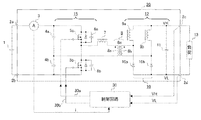
図1は、この発明の実施の形態1による電力変換装置としてのDC/DCコンバータ装置および車載電源装置の構成図である。図1に示すように、車載電源装置は、車両の走行用モータ駆動用の高圧のバッテリ1と、バッテリ1の電圧を異なる電圧に変換して負荷13に電力供給するためのDC/DCコンバータ装置によって構成される。DC/DCコンバータ装置は主回路20と制御回路30とを備え、DC/DCコンバータ装置の主回路20を、以下、単にDC/DCコンバータ20と称す。
DC/DCコンバータ20は、絶縁されたトランス8と、該トランス8の一次側に接続されて入力端子2a−2b間の直流電圧を交流電圧に変換するインバータ部15と、トランス8の二次側に接続された整流回路10と、整流された電圧を平滑して出力端子2c−2d間に出力する平滑回路12とを備える。Embodiment 1 FIG.
Hereinafter, a power conversion device and an in-vehicle power supply device according to Embodiment 1 of the present invention will be described with reference to the drawings.
1 is a configuration diagram of a DC / DC converter device and an in-vehicle power supply device as a power conversion device according to Embodiment 1 of the present invention. As shown in FIG. 1, the in-vehicle power supply device includes a high voltage battery 1 for driving a vehicle driving motor and a DC / DC converter device for converting the voltage of the battery 1 into a different voltage and supplying power to a
The DC /
インバータ部15は、直流母線間に直列接続される第1、第2の分圧用コンデンサ4a、4b、および2直列の半導体スイッチング素子としての第1、第2のMOSFET(電界効果型トランジスタ)5a、5bを有するハーフブリッジインバータにて構成される。第1、第2のMOSFET5a、5bは、それぞれダイオードが逆並列接続されている。なお、このダイオードは素子が内蔵する寄生ダイオードを用いても良い。このインバータ部15は、第1、第2のMOSFET5a、5bのスイッチング時の素子の両端電圧がほぼゼロ電圧にできるゼロ電圧スイッチング回路であり、第1、第2のMOSFET5a、5bにはそれぞれ並列に第1、第2のコンデンサ6a、6bが接続される。また、第1、第2のMOSFET5a、5bとトランス8の一次巻線8aとの間の交流出力線にはインダクタ7が接続される。
また、整流回路10はダイオード10a、10bにて構成され、平滑回路12は、インダクタ9a、9bおよび平滑コンデンサ11にて構成される。
さらに、DC/DCコンバータ20を流れる回路電流としての電流iを検出する電流検出器3が、この場合、インバータ部15の入力側の直流母線に設けられている。The
The
Further, in this case, a
DC/DCコンバータ20の外部には、インバータ部15を出力制御する制御回路30が配置される。制御回路30には、出力端子2c、2dの各電位VH、VLと、電流検出器3にて検出された電流iとが入力され、インバータ部15の第1、第2のMOSFET5a、5bへの第1、第2のゲート信号30a、30bを生成して出力する。
A
車載電源装置の各部の接続の詳細を以下に示す。
バッテリ1は入力端子2a−2b間に接続される。入力端子2aは、電流検出器3の一端に接続され、電流検出器3の他端は第1の分圧用コンデンサ4aの第1の端子および第1のMOSFET5aのドレイン端子に各々接続される。入力端子2bは、第2の分圧用コンデンサ4bの第1の端子および第2のMOSFET5bのソース端子に各々接続される。第1の分圧用コンデンサ4aの第2の端子と第2の分圧用コンデンサ4bの第2の端子が互いに接続され、第1のMOSFET5aのソース端子と第2のMOSFET5bのドレイン端子が互いに接続される。第1のMOSFET5aと第2のMOSFET5bの接続点とインダクタ7の一端が接続され、インダクタ7の他端とトランス8の一次巻線8aの第1の端子が接続される。第1のコンデンサ6aは第1のMOSFET5aのドレイン−ソース間に接続され、第2のコンデンサ6bは第2のMOSFET5bのドレイン−ソース間に接続される。Details of the connection of each part of the in-vehicle power supply device are shown below.
The battery 1 is connected between the
トランス8の一次巻線8aの第2の端子と、第1の分圧用コンデンサ4aおよび第2の分圧用コンデンサ4bの接続点が接続される。トランス8の二次巻線8bの第1の端子と、インダクタ9aの第1の端子およびダイオード10aのカソード端子が各々接続され、トランス8の二次巻線8bの第2の端子と、インダクタ9bの第1の端子およびダイオード10bのカソード端子が各々接続される。平滑コンデンサ11が出力端子2c−2d間に接続される。各インダクタ9a、9bの第2の端子が平滑コンデンサ11の一端に各々接続され、平滑コンデンサ11の他端に各ダイオード10a、10bのカソード端子が各々接続される。そして、負荷13が出力端子2c−2d間に接続される。
制御回路30は、第1、第2のMOSFET5a、5bのゲート端子が接続されると共に、出力端子2c、2dおよび電流検出器3に接続される。A connection point between the second terminal of the primary winding 8a of the transformer 8 and the first voltage dividing capacitor 4a and the second voltage dividing capacitor 4b is connected. The first terminal of the secondary winding 8b of the transformer 8, the first terminal of the
The
このように構成される車載電源装置の動作について、以下に説明する。
バッテリ1の電圧Vinが入力端子2a−2b間に接続されると、第1の分圧用コンデンサ4aおよび第2の分圧用コンデンサ4bにより1/2・Vinずつに分圧される。図2は、インバータ部15の第1、第2のMOSFET5a、5bへの第1、第2のゲート信号30a、30bを示すもので、第1のMOSFET5aおよび第2のMOSFET5bは相補的にオンオフ動作を繰り返す。第1のMOSFET5aおよび第2のMOSFET5bが共にオフになる期間をデッドタイムtdとする。なお、図2において、Tsはスイッチングの周期、Tonは各第1、第2のMOSFET5a、5bのオン期間、Toffは、半周期Ts/2での各第1、第2のMOSFET5a、5bのTon後のオフ期間であり、この場合、Toff=tdとなる。The operation of the in-vehicle power supply device configured as described above will be described below.
When the voltage Vin of the battery 1 is connected between the
まず、第1のMOSFET5aがオン状態で第2のMOSFET5bがオフ状態の時、トランス8の一次側には、第1の分圧用コンデンサ4a→第1のMOSFET5a→インダクタ7→トランス一次巻線8aの経路で電流が流れ、トランス一次巻線8aに1/2・Vinの電圧が印加される。その結果、トランス8の二次側には、トランス二次巻線8bにトランス巻数比で決まる電圧が誘起し、トランス二次巻線8b→インダクタ9a→平滑コンデンサ11→ダイオード10bの経路で電流が流れ、トランス8の一次側から二次側に電力伝達が行われる。
First, when the
次に、第1のMOSFET5aがオフしてデッドタイムtd期間に入ると、インダクタ7は電流を流し続けようとする特性があるので、トランス8の一次側には、インダクタ7→トランス一次巻線8a→第1の分圧用コンデンサ4a→コンデンサ6aの経路と、インダクタ7→トランス一次巻線8a→第2の分圧用コンデンサ4b→コンデンサ6bの経路とで電流が流れる。この時、第1のMOSFET5aの両端電圧はコンデンサ6aの作用により、電圧の上昇を遅くすることができ、このようなスイッチングが一般にゼロ電圧スイッチングと呼ばれるもので、スイッチング損失がほぼゼロに低減される。
Next, when the
また、コンデンサ6aとコンデンサ6bとの各電圧の和は第1、第2の分圧用コンデンサ4a、4bの電圧和であるVinに等しくなるので、コンデンサ6aの両端電圧の上昇に応じてコンデンサ6bの両端電圧は下降する。この状態は、コンデンサ6aの電圧が、第1、第2の分圧用コンデンサ4a、4bの電圧和Vinにほぼ等しくなり、コンデンサ6bの電圧がほぼゼロになるまで継続する。
またこの時、トランス8の二次側には、インダクタ9a→平滑コンデンサ11→ダイオード10aの経路と、インダクタ9b→平滑コンデンサ11→ダイオード10bの経路とで電流が流れる。Further, since the sum of the voltages of the capacitor 6a and the capacitor 6b is equal to Vin which is the voltage sum of the first and second voltage dividing capacitors 4a and 4b, the voltage of the capacitor 6b is increased according to the rise of the voltage across the capacitor 6a. The voltage at both ends falls. This state continues until the voltage of the capacitor 6a becomes substantially equal to the voltage sum Vin of the first and second voltage dividing capacitors 4a and 4b, and the voltage of the capacitor 6b becomes substantially zero.
At this time, a current flows on the secondary side of the transformer 8 through a path of
次に、コンデンサ6aの電圧が、Vinにほぼ等しくなり、コンデンサ6bの電圧がほぼゼロになると、トランス8の一次側には、インダクタ7→トランス一次巻線8a→第2の分圧用コンデンサ4b→第2のMOSFET5bの逆並列ダイオードの経路で電流が流れる。
Next, when the voltage of the capacitor 6a becomes substantially equal to Vin and the voltage of the capacitor 6b becomes almost zero, the
次に、第2のMOSFET5bがオンするが、この時、第2のMOSFET5bの両端にかかる電圧(コンデンサ6bの電圧)はほぼゼロで、ゼロ電圧スイッチングとなり、第2のMOSFET5bのスイッチング損失はほぼゼロである。
そして、第1のMOSFET5aがオフ状態で第2のMOSFET5bがオン状態の時、トランス8の一次側には、第2の分圧用コンデンサ4b→トランス一次巻線8a→インダクタ7→第2のMOSFET5bの経路で電流が流れ、トランス一次巻線8aに−1/2・Vinの電圧が印加される。その結果、トランス8の二次側には、トランス二次巻線8bにトランス巻数比で決まる電圧が誘起し、トランス二次巻線8b→インダクタ9b→平滑コンデンサ11→ダイオード10aの経路で電流が流れ、トランス8の一次側から二次側に電力伝達が行われる。Next, the second MOSFET 5b is turned on. At this time, the voltage applied to both ends of the second MOSFET 5b (the voltage of the capacitor 6b) is almost zero and zero voltage switching is performed, and the switching loss of the second MOSFET 5b is almost zero. It is.
When the
次に、第2のMOSFET5bがオフしてデッドタイムtd期間に入ると、電流を流し続けようとするインダクタ7の特性により、トランス8の一次側には、インダクタ7→コンデンサ6b→第2の分圧用コンデンサ4b→トランス一次巻線8aの経路と、インダクタ7→コンデンサ6a→第1の分圧用コンデンサ4a→トランス一次巻線8aの経路とで電流が流れる。この時、第2のMOSFET5bの両端電圧はコンデンサ6bの作用により、電圧の上昇を遅くすることができ、ゼロ電圧スイッチングによるオフとなる。
Next, when the second MOSFET 5b is turned off and the dead time td is entered, the
また、コンデンサ6bの両端電圧の上昇に応じてコンデンサ6aの両端電圧は下降し、この状態は、コンデンサ6bの電圧が、第1、第2の分圧用コンデンサ4a、4bの電圧和Vinにほぼ等しくなり、コンデンサ6aの電圧がほぼゼロになるまで継続する。
またこの時、トランス8の二次側には、インダクタ9a→平滑コンデンサ11→ダイオード10aの経路と、インダクタ9b→平滑コンデンサ11→ダイオード10bの経路とで電流が流れる。Further, as the voltage across the capacitor 6b rises, the voltage across the capacitor 6a falls. In this state, the voltage across the capacitor 6b is substantially equal to the voltage sum Vin of the first and second voltage dividing capacitors 4a and 4b. This continues until the voltage of the capacitor 6a becomes almost zero.
At this time, a current flows on the secondary side of the transformer 8 through a path of
次に、コンデンサ6bの電圧が、Vinにほぼ等しくなり、コンデンサ6aの電圧がほぼゼロになると、トランス8の一次側には、インダクタ7→第1のMOSFET5aの逆並列ダイオード→第1の分圧用コンデンサ4a→トランス一次巻線8aの経路で電流が流れる。
その後、第1のMOSFET5aがオンして、第1のMOSFET5aがオン状態で第2のMOSFET5bがオフ状態の時に戻る。この時も、第1のMOSFET5aの両端にかかる電圧(コンデンサ6aの電圧)はほぼゼロで、ゼロ電圧スイッチングとなり、第1のMOSFET5aのスイッチング損失はほぼゼロである。Next, when the voltage of the capacitor 6b becomes substantially equal to Vin and the voltage of the capacitor 6a becomes almost zero, the
Thereafter, the
上述したような第1、第2のMOSFET5a、5bのゼロ電圧スイッチングの際には、各第1、第2のMOSFET5a、5bに並列接続されたコンデンサ6a、6bが作用する。各第1、第2のMOSFET5a、5bのゼロ電圧スイッチングが成立するためには、スイッチングにおけるデッドタイムtd期間中に、コンデンサ6a、6bの電圧が第1、第2の分圧用コンデンサ4a、4bの電圧和Vinまで増加する、あるいはゼロ電圧近辺まで低下することが必要である。第1、第2のMOSFET5a、5bのオンオフにより、コンデンサ6a、6bの電圧が第1、第2の分圧用コンデンサ4a、4bの電圧和Vinまで増加する、あるいはゼロ電圧近辺まで低下するために要する時間を、以下、コンデンサ6a、6bの充放電完了時間と称す。
コンデンサ6a、6bの電圧は、コンデンサ6a、6bを充放電する電流であるインダクタ7の電流によって変化する。このため、負荷13が軽くなりDC/DCコンバータ20の出力電力が小さい場合、すなわちインダクタ7の電流が低下すると、コンデンサ6a、6bの充放電完了時間が増大する。In the zero voltage switching of the first and
The voltages of the capacitors 6a and 6b vary depending on the current of the
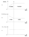
図3は、インバータ部15の第1、第2のMOSFET5a、5bの制御および動作について説明する図である。図3に示すように、制御回路30は、電流検出器3からの電流iに応じて制御を切り換える。インダクタ7の電流は負荷電流に依存し、電流検出器3からの電流iも同様に負荷電流に依存するため、コンデンサ6a、6bの電圧は、負荷電流に依存する電流iによって変化すると言うことができる。
制御回路30は、電流iが所定値iaを超える領域、即ち負荷13が中負荷〜定格負荷の負荷領域においては、PWM制御を用いてインバータ部15を制御し、電流iが所定値ia以下になると、即ち負荷13が所定負荷より軽い軽負荷領域になるとPFM制御(Pulse Frequency Modulation制御)に切り換える。
周波数が一定のPWM制御ではデッドタイムtdが固定であるが、低電流領域でのPFM制御では、電流iの減少に伴ってデッドタイムtdが長くなるように周波数を低減させる。そして所望の出力電圧を得るデューティ比を変化させずに保持する。FIG. 3 is a diagram illustrating the control and operation of the first and
The
In the PWM control with a constant frequency, the dead time td is fixed, but in the PFM control in the low current region, the frequency is reduced so that the dead time td becomes longer as the current i decreases. Then, the duty ratio for obtaining a desired output voltage is maintained without being changed.
上述したように、負荷13が軽くなりDC/DCコンバータ20の出力電力が小さい場合、即ち電流iが低下すると、第1、第2のMOSFET5a、5bのスイッチング時におけるコンデンサ6a、6bの充放電完了時間が増大する。この実施の形態では、電流iが所定値ia以下になるとPFM制御に切り換えて、電流iの減少に伴ってデッドタイムtdを長くして第1、第2のMOSFET5a、5bをスイッチング制御する。このデッドタイムtdは、電流iの減少に伴って増大するコンデンサ6a、6bの充放電完了時間より長くなるように設定される。
As described above, when the
これにより、広い負荷範囲において、第1、第2のMOSFET5a、5bのスイッチングにおけるデッドタイムtd期間中に、コンデンサ6a、6bの電圧が第1、第2の分圧用コンデンサ4a、4bの電圧和Vinまで増加する、あるいはゼロ電圧近辺まで低下することが可能になり、ゼロ電圧スイッチングが信頼性良く安定して行える。これにより、電力損失を大きく低減でき、変換効率の高いDC/DCコンバータ装置、およびそれを用いた車載電源装置が得られる。
Thus, in the wide load range, the voltage of the capacitors 6a and 6b becomes the voltage sum Vin of the first and second voltage dividing capacitors 4a and 4b during the dead time td in the switching of the first and
なお、上記実施の形態では、電流検出器3は、インバータ部15の入力側の直流母線に接続して入力電流を検出したが、DC/DCコンバータ20を流れる電流で、負荷電流に依存して変化する電流を検出するものであれば、これに限るものではない。
In the above embodiment, the
また、上記実施の形態1では、2直列の半導体スイッチング素子5a、5bとしてMOSFETを用いて説明を行ったが、バイポーラトランジスタ、または絶縁型バイポーラトランジスタ(IGBT)、またはシリコンカーバイドトランジスタ、またはワイドバンドギャップ半導体によって形成されたMOSFETを用いても同様の効果が得られる。
ワイドバンドギャップ半導体は、シリコンに比べてバンドギャップが大きい半導体であり、例えば、炭化珪素、窒化ガリウム系材料又はダイヤモンドがある。このようなワイドバンドギャップ半導体によって形成されたスイッチング素子は、耐電圧性が高く、許容電流密度も高いため、スイッチング素子の小型化が可能であり、これら小型化されたスイッチング素子を用いることにより、車載電源装置の小型化が促進できる。更に電力損失が低いため、スイッチング素子の高効率化が可能であり、車載電源装置の高効率化が図れる。
またワイドバンドギャップ半導体から成るスイッチング素子は耐熱性も高いため、通常、車載電源装置に併設されているヒートシンクの放熱フィンの小型化や、水冷部の空冷化が可能であるので、車載電源装置の一層の小型化が可能になる。In the first embodiment, MOSFETs are used as the two series
A wide band gap semiconductor is a semiconductor having a larger band gap than silicon, for example, silicon carbide, gallium nitride-based material, or diamond. Since the switching element formed of such a wide band gap semiconductor has high voltage resistance and high allowable current density, the switching element can be reduced in size. By using these reduced switching elements, Miniaturization of the in-vehicle power supply device can be promoted. Furthermore, since the power loss is low, the efficiency of the switching element can be increased, and the efficiency of the in-vehicle power supply device can be increased.
In addition, since switching elements made of wide band gap semiconductors have high heat resistance, it is usually possible to reduce the size of the heat sink fins of the heat sink provided in the in-vehicle power supply device and to cool the water cooling part. Further downsizing becomes possible.
また、上記実施の形態1では、インダクタ7を独立した素子として説明を行ったが、トランス8の漏れインダクタンスを用いても良く、同様の効果が得られる。
In the first embodiment, the
さらにまた、第1、第2のMOSFET5a、5bにそれぞれ並列接続される第1、第2のコンデンサ6a、6bは、第1のMOSFET5aおよび第2のMOSFET5bの両端に寄生する寄生容量を用いても良く、同様の効果が得られる。
Furthermore, the first and second capacitors 6a and 6b connected in parallel to the first and
また、上記実施の形態1では、インバータ部15をハーフブリッジインバータで構成したが、それ以外の種々のインバータ回路にも適用でき同様の効果が得られる。
Moreover, in the said Embodiment 1, although the
また、上記実施の形態1では、トランス8の二次側の回路構成に、倍電流整流回路構成を用いて説明したが、センタータップ整流やダイオードブリッジ整流の回路構成としても良く、同様の効果が得られる。 In the first embodiment, the circuit configuration on the secondary side of the transformer 8 has been described by using a double current rectifier circuit configuration. However, a circuit configuration of center tap rectification or diode bridge rectification may be used, and similar effects can be obtained. can get.
また、上記実施の形態1では、整流回路10としてダイオード10a、10bを用いたダイオード整流を示したが、半導体スイッチング素子を備えて同期整流回路を構成しても良い。その場合、制御回路30は、整流回路内の半導体スイッチング素子を、インバータ部15の第1、第2のMOSFET5a、5bに同期させてスイッチング制御する。これにより整流回路での導通損失が低減できる。
また、整流回路内の半導体スイッチング素子をワイドバンドギャップ半導体によって形成することにより、さらに低損失で小型化、高効率化が図れる。In the first embodiment, diode rectification using the
Further, by forming the semiconductor switching element in the rectifier circuit with a wide band gap semiconductor, it is possible to further reduce the size and increase the efficiency with low loss.
また、上記実施の形態1では、インバータ部15のPFM制御期間では、デッドタイムtdは電流低下に伴って直線的に増大するものを図示したが、曲線的あるいは階段状などにより増大しても良く、電流低下に伴って増大するコンデンサ6a、6bの充放電完了時間より長くなるように設定されるものであれば良い。
In the first embodiment, the dead time td increases linearly as the current decreases in the PFM control period of the
また、上記実施の形態1では、DC/DCコンバータ装置は車載電源装置に適用するものを示したが、車両用以外にも適用可能で、同様の効果が得られる。また、DC/DCコンバータ装置は、絶縁のためのトランス8が無い構成としても良い。 In the first embodiment, the DC / DC converter device is applied to the in-vehicle power supply device. However, the DC / DC converter device can be applied to other than the vehicle and the same effect can be obtained. The DC / DC converter device may be configured without the transformer 8 for insulation.
実施の形態2.
次に、この発明の実施の形態2について説明する。
この実施の形態2では、上記実施の形態1の図1で示した同様の回路構成の電力変換装置および車載電源装置を用い、制御回路30には、出力端子2c、2dの各電位VH、VLと、電流検出器3にて検出された電流iとが入力され、インバータ部15の第1、第2のMOSFET5a、5bへ、図2で示した同様の第1、第2のゲート信号30a、30bを生成して出力する。この場合、制御回路30による第1、第2のMOSFET5a、5bの制御の方法が上記実施の形態1と異なり、以下に示す。
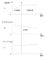
図4は、実施の形態2による、インバータ部15の第1、第2のMOSFET5a、5bの制御および動作について説明する図である。図4に示すように、制御回路30は、電流iが所定値ibを超える領域、即ち負荷13が中負荷〜定格負荷の負荷領域においては、PWM制御を用いてインバータ部15を制御し、電流iが所定値ib以下になると、即ち負荷13が所定負荷より軽い軽負荷領域になるとPFM制御に切り換える。
Next, a second embodiment of the present invention will be described.
In the second embodiment, the power conversion device and the in-vehicle power supply device having the same circuit configuration shown in FIG. 1 of the first embodiment are used, and the
FIG. 4 is a diagram illustrating the control and operation of the first and
通常、所望の出力電圧を得るためのデューティ比にはある程度余裕があり、周波数が一定のPWM制御においても、デューティ比が許容される範囲で、電流iの減少に伴ってデッドタイムtdが長くなるように第1、第2のMOSFET5a、5bを制御する。そして、低電流領域でのPFM制御では、電流iの減少に伴ってデッドタイムtdが長くなるように周波数を低減させ、デューティ比を変化させずに保持する。
このデッドタイムtdは、電流iの減少に伴って増大するコンデンサ6a、6bの充放電完了時間より長くなるように設定される。Normally, the duty ratio for obtaining a desired output voltage has a certain margin, and even in PWM control with a constant frequency, the dead time td becomes longer as the current i decreases within the allowable range of the duty ratio. Thus, the first and
The dead time td is set to be longer than the charge / discharge completion time of the capacitors 6a and 6b, which increases as the current i decreases.
上述したように、負荷13が軽くなりDC/DCコンバータ20の出力電力が小さい場合、即ち電流iが低下すると、第1、第2のMOSFET5a、5bのスイッチング時におけるコンデンサ6a、6bの充放電完了時間が増大するが、この充放電完了時間よりデッドタイムtdを長くなるように設定して第1、第2のMOSFET5a、5bを制御する。
これにより、広い負荷範囲において、第1、第2のMOSFET5a、5bのスイッチングにおけるデッドタイムtd期間中に、コンデンサ6a、6bの電圧が第1、第2の分圧用コンデンサ4a、4bの電圧和Vinまで増加する、あるいはゼロ電圧近辺まで低下することが可能になり、ゼロ電圧スイッチングが信頼性良く安定して行える。これにより、上記実施の形態1と同様に、電力損失を大きく低減でき、変換効率の高いDC/DCコンバータ装置、およびそれを用いた車載電源装置が得られる。As described above, when the
Thus, in the wide load range, the voltage of the capacitors 6a and 6b becomes the voltage sum Vin of the first and second voltage dividing capacitors 4a and 4b during the dead time td in the switching of the first and
なお、上述した上記実施の形態1に適用可能な種々の変形例は、同様に適用でき同様の効果が得られる。 The various modifications that can be applied to the above-described first embodiment can be applied in the same manner, and similar effects can be obtained.
実施の形態3.
次に、この発明の実施の形態3について説明する。
この実施の形態3においても、上記実施の形態1と同様の回路構成の電力変換装置および車載電源装置を用い、制御回路30による第1、第2のMOSFET5a、5bの制御の方法が上記実施の形態1と異なる。
図5は、実施の形態3による、インバータ部15の第1、第2のMOSFET5a、5bの制御および動作について説明する図である。図5に示すように、制御回路30は、PFM制御により第1、第2のMOSFET5a、5bを制御する。そして、電流iの減少に伴ってデッドタイムtdが長くなるように周波数を低減させ、所望の出力電圧を得るデューティ比を変化させずに保持する。このデッドタイムtdは、電流iの減少に伴って増大するコンデンサ6a、6bの充放電完了時間より長くなるように設定される。
Next, a third embodiment of the present invention will be described.
Also in the third embodiment, the method for controlling the first and
FIG. 5 is a diagram for explaining control and operation of the first and
上述したように、負荷13が軽くなりDC/DCコンバータ20の出力電力が小さい場合、即ち電流iが低下すると、第1、第2のMOSFET5a、5bのスイッチング時におけるコンデンサ6a、6bの充放電完了時間が増大するが、この充放電完了時間よりデッドタイムtdを長くなるように設定して第1、第2のMOSFET5a、5bを制御する。
これにより、広い負荷範囲において、第1、第2のMOSFET5a、5bのスイッチングにおけるデッドタイムtd期間中に、コンデンサ6a、6bの電圧が第1、第2の分圧用コンデンサ4a、4bの電圧和Vinまで増加する、あるいはゼロ電圧近辺まで低下することが可能になり、ゼロ電圧スイッチングが信頼性良く安定して行える。これにより、上記実施の形態1と同様に、電力損失を大きく低減でき、変換効率の高いDC/DCコンバータ、およびそれを用いた車載電源装置が得られる。As described above, when the
Thus, in the wide load range, the voltage of the capacitors 6a and 6b becomes the voltage sum Vin of the first and second voltage dividing capacitors 4a and 4b during the dead time td in the switching of the first and
なお、上述した上記実施の形態1に適用可能な種々の変形例は、同様に適用でき同様の効果が得られる。 The various modifications that can be applied to the above-described first embodiment can be applied in the same manner, and similar effects can be obtained.
実施の形態4.
次に、この発明の実施の形態4について説明する。
図6は、この発明の実施の形態4による電力変換装置としてのDC/DCコンバータ装置および車載電源装置の構成図である。図6に示すように、制御回路30には、出力端子2c、2dの各電位VH、VLと、電流検出器3にて検出された電流iと、さらに第2のMOSFET5bのドレイン端子、ソース端子の各電位Vd、Vsが入力され、インバータ部15の第1、第2のMOSFET5a、5bへ第1、第2のゲート信号30a、30bを生成して出力する。その他の構成は、上記実施の形態1と同様である。
Next, a fourth embodiment of the present invention will be described.
FIG. 6 is a configuration diagram of a DC / DC converter device and an in-vehicle power supply device as a power conversion device according to
制御回路30の基本の制御は、上記実施の形態1と同様である。電流iが所定値iaを超える領域、即ち負荷13が中負荷〜定格負荷の負荷領域においては、PWM制御を用いてデッドタイムtdを固定にしてインバータ部15を制御し、電流iが所定値ia以下になると、即ち負荷13が所定負荷より軽い軽負荷領域になるとPFM制御に切り換える。そして、低電流領域でのPFM制御では、電流iの減少に伴ってデッドタイムtdが長くなるように周波数を低減させる。そして所望の出力電圧を得るデューティ比を変化させずに保持する。
The basic control of the
この場合、制御回路30では、第2のMOSFET5bのドレイン端子、ソース端子の各電位Vd、Vsから、第2のMOSFET5bの両端電圧を検出して監視し、該両端電圧に基づいて、第1、第2のMOSFET5a、5bがゼロ電圧スイッチングするように第1、第2のMOSFET5a、5bのスイッチングを調整する。第1、第2のMOSFET5a、5bがゼロ電圧スイッチングするのは、コンデンサ6a、6bの電圧、即ち、第1、第2のMOSFET5a、5bの両端電圧が、第1、第2の分圧用コンデンサ4a、4bの電圧和Vinとほぼ等しいか、ほぼ0に等しい時である。このため、第2のMOSFET5bの両端電圧を監視し、この電圧が、Vinとほぼ等しいか、ほぼ0に等しい時に第1、第2のMOSFET5a、5bがオンオフするように、スイッチングのタイミングを調整する。
これにより、上記実施の形態1と同様の効果が得られると共に、第1、第2のMOSFET5a、5bが確実にゼロ電圧スイッチングすることができ、電力損失をさらに低減でき、変換効率の高いDC/DCコンバータ装置、およびそれを用いた車載電源装置が得られる。In this case, the
As a result, the same effects as those of the first embodiment can be obtained, and the first and
なお、上記実施の形態4では、制御回路30の基本の制御は、上記実施の形態1と同様である場合を示したが、上記実施の形態2または3と同様にしても良く、いずれも第1、第2のMOSFET5a、5bが確実にゼロ電圧スイッチングすることができ、電力損失をさらに低減でき、変換効率の高いDC/DCコンバータ装置、およびそれを用いた車載電源装置が得られる。
In the fourth embodiment, the basic control of the
また、上述した上記実施の形態1に適用可能な種々の変形例は、同様に適用でき同様の効果が得られる。 Moreover, the various modifications applicable to the above-described first embodiment can be applied in the same manner, and the same effect can be obtained.
実施の形態5.
次に、この発明の実施の形態5について説明する。
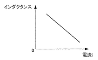
この実施の形態5では、上記各実施の形態1〜4において、インダクタ7に可変特性を有するものを用いる。図7は、実施の形態5によるインダクタ7の特性図であり、電流に応じてインダクタンスを可変とし、電流が増加するとインダクタンスを減少させる。
インダクタンスが一定の場合では、DC/DCコンバータ20に流れる電流が増加すると、第1、第2のMOSFET5a、5bのスイッチング時におけるインダクタ7での転流時間が増大する。この実施の形態では、インダクタ7は、電流の増加に伴いインダクタンスを減少させるため、転流時間を短縮することができる。このため、DC/DCコンバータ20は、さらに低損失で電力変換効率が向上する。Embodiment 5 FIG.
Next, a fifth embodiment of the present invention will be described.
In the fifth embodiment, the
When the inductance is constant, when the current flowing through the DC /
また、ゼロ電圧スイッチングはインダクタ7の転流を利用して行っているもので、この場合、デッドタイムtdの設定は、電流iと、電流iに応じて変化するインダクタ7のインダクタンスとの双方に基づいて、例えば、PFM制御においては周波数を非線形に変化させることにより、ゼロ電圧スイッチングできるように、また所望の出力電圧が得られるように設定する。これにより、ゼロ電圧スイッチングが確実に行えると共に、動作周波数の下限値を上昇させることができるためDC/DCコンバータ20内の磁性部品が小型化できる。
Also, zero voltage switching is performed using the commutation of the
なお、この発明は、その発明の範囲内において、各実施の形態を自由に組み合わせたり、各実施の形態を適宜、変形、省略することが可能である。 It should be noted that within the scope of the present invention, the embodiments can be freely combined, or the embodiments can be appropriately modified or omitted.
この発明に係る電力変換装置は、2直列の半導体スイッチング素子を備えて直流電力を交流電力に変換するインバータ部と、該インバータ部の交流出力を整流する整流回路と、整流された電圧を平滑して負荷に直流電力を出力する平滑回路とを備えたDC/DCコンバータと、上記インバータ部を制御する制御回路とを備える。上記インバータ部は、上記各半導体スイッチング素子に並列接続されたコンデンサと、交流出力線に接続されたインダクタとを備える。そして上記制御回路は、上記各半導体スイッチ素子がゼロ電圧スイッチングするように、上記DC/DCコンバータを流れる回路電流に応じて、上記2直列の半導体スイッチング素子が共にオフする期間であるデッドタイムを変化させ、該回路電流が少なくとも低電流領域ではPFM制御を用いて上記インバータ部を制御し、上記インダクタは、上記回路電流に応じてインダクタンスを可変とし、上記回路電流が増加すると上記インダクタンスを減少させるものである。
またこの発明に係る電力変換装置は、2直列の半導体スイッチング素子を備えて直流電力を交流電力に変換するインバータ部と、該インバータ部の交流出力を整流する整流回路と、整流された電圧を平滑して負荷に直流電力を出力する平滑回路とを備えたDC/DCコンバータと、上記インバータ部を制御する制御回路とを備える。上記インバータ部は、上記各半導体スイッチング素子に並列接続されたコンデンサと、交流出力線に接続されたインダクタとを備え、上記2直列の半導体スイッチング素子の一方の両端電圧を検出する。そして上記制御回路は、上記各半導体スイッチ素子がゼロ電圧スイッチングするように、上記DC/DCコンバータを流れる回路電流に応じて、上記2直列の半導体スイッチング素子が共にオフする期間であるデッドタイムを変化させ、該回路電流が少なくとも所定値以下となる領域ではPFM制御を用いて上記インバータ部を制御し、検出された上記両端電圧に応じて上記2直列の半導体スイッチング素子のスイッチングを調整するものである。
A power converter according to the present invention includes an inverter unit that includes two series semiconductor switching elements and converts DC power into AC power, a rectifier circuit that rectifies the AC output of the inverter unit, and smoothes the rectified voltage. And a DC / DC converter including a smoothing circuit that outputs DC power to the load, and a control circuit that controls the inverter unit. The inverter unit includes a capacitor connected in parallel to each of the semiconductor switching elements and an inductor connected to an AC output line. The control circuit changes a dead time, which is a period during which both of the two series semiconductor switching elements are turned off, in accordance with a circuit current flowing through the DC / DC converter so that the semiconductor switching elements perform zero voltage switching. The inverter unit is controlled using PFM control at least in a low current region of the circuit current, and the inductor is variable in inductance according to the circuit current, and decreases when the circuit current increases. It is.
The power converter according to the present invention includes an inverter unit that includes two series semiconductor switching elements and converts DC power into AC power, a rectifier circuit that rectifies the AC output of the inverter unit, and smoothes the rectified voltage. And a DC / DC converter including a smoothing circuit that outputs DC power to a load, and a control circuit that controls the inverter unit. The inverter unit includes a capacitor connected in parallel to each of the semiconductor switching elements and an inductor connected to an AC output line, and detects a voltage across one of the two series semiconductor switching elements. The control circuit changes a dead time, which is a period during which both of the two series semiconductor switching elements are turned off, in accordance with a circuit current flowing through the DC / DC converter so that the semiconductor switching elements perform zero voltage switching. In the region where the circuit current is at least a predetermined value or less, the inverter unit is controlled using PFM control, and the switching of the two series semiconductor switching elements is adjusted according to the detected voltage across the both ends. .
Claims (12)
上記インバータ部は、上記各半導体スイッチング素子に並列接続されたコンデンサと、交流出力線に接続されたインダクタとを備え、
上記制御回路は、上記各半導体スイッチ素子がゼロ電圧スイッチングするように、上記DC/DCコンバータを流れる回路電流に応じて、上記2直列の半導体スイッチング素子が共にオフする期間であるデッドタイムを変化させ、該回路電流が少なくとも所定値以下となる領域ではPFM制御を用いて上記インバータ部を制御する、
電力変換装置。An inverter unit that includes two series semiconductor switching elements and converts DC power to AC power; a rectifier circuit that rectifies the AC output of the inverter unit; and a smoother that smoothes the rectified voltage and outputs DC power to the load In a power conversion device including a DC / DC converter including a circuit and a control circuit for controlling the inverter unit,
The inverter unit includes a capacitor connected in parallel to each of the semiconductor switching elements, and an inductor connected to an AC output line,
The control circuit changes a dead time which is a period during which both of the two series semiconductor switching elements are turned off according to a circuit current flowing through the DC / DC converter so that each of the semiconductor switching elements performs zero voltage switching. In the region where the circuit current is at least a predetermined value or less, the inverter unit is controlled using PFM control.
Power conversion device.
請求項1に記載の電力変換装置。The control circuit controls the inverter unit using PWM control in a region where the circuit current exceeds the predetermined value, and switches to PFM control when the circuit current falls below the predetermined value.
The power conversion device according to claim 1.
請求項1または2に記載の電力変換装置。The control circuit increases the dead time when the circuit current decreases.
The power converter according to claim 1 or 2.
上記制御回路は、検出された電圧に応じて上記2直列の半導体スイッチング素子のスイッチングを調整する、
請求項1または2に記載の電力変換装置。A voltage across one of the two series semiconductor switching elements is detected;
The control circuit adjusts switching of the two series semiconductor switching elements according to the detected voltage.
The power converter according to claim 1 or 2.
請求項1または2に記載の電力変換装置。The inductor has an inductance variable according to the circuit current, and decreases the inductance when the circuit current increases.
The power converter according to claim 1 or 2.
上記制御回路は、上記整流回路内の上記半導体スイッチング素子を、上記インバータ部の上記2直列スイッチング素子に同期させてスイッチング制御する、
請求項1または2に記載の電力変換装置。The rectifier circuit includes a semiconductor switching element,
The control circuit controls the switching of the semiconductor switching element in the rectifier circuit in synchronization with the two series switching elements of the inverter unit.
The power converter according to claim 1 or 2.
請求項1または2に記載の電力変換装置。The semiconductor switching element in the rectifier circuit is formed of a wide band gap semiconductor having a wider band gap than silicon.
The power converter according to claim 1 or 2.
請求項1または2に記載の電力変換装置。Each of the semiconductor switching elements in the inverter unit is formed of a wide band gap semiconductor having a wider band gap than silicon.
The power converter according to claim 1 or 2.
走行用モータ駆動用のバッテリを備えた車載電源装置において、
上記インバータ部は、上記各半導体スイッチング素子に並列接続されたコンデンサと、交流出力線に接続されたインダクタとを備えて、上記バッテリから直流電力が入力され、
上記制御回路は、上記各半導体スイッチ素子がゼロ電圧スイッチングするように、上記DC/DCコンバータを流れる回路電流に応じて、上記2直列の半導体スイッチング素子が共にオフする期間であるデッドタイムを変化させ、該回路電流が少なくとも所定値以下となる領域ではPFM制御を用いて上記インバータ部を制御する、
車載電源装置。An inverter unit that includes two series semiconductor switching elements and converts DC power to AC power; a rectifier circuit that rectifies the AC output of the inverter unit; and a smoother that smoothes the rectified voltage and outputs DC power to the load In a power converter including a DC / DC converter including a circuit and a control circuit for controlling the inverter unit, and an in-vehicle power supply including a battery for driving a traveling motor,
The inverter unit includes a capacitor connected in parallel to each of the semiconductor switching elements and an inductor connected to an AC output line, and DC power is input from the battery.
The control circuit changes a dead time which is a period during which both of the two series semiconductor switching elements are turned off according to a circuit current flowing through the DC / DC converter so that each of the semiconductor switching elements performs zero voltage switching. In the region where the circuit current is at least a predetermined value or less, the inverter unit is controlled using PFM control.
In-vehicle power supply.
Priority Applications (1)
| Application Number | Priority Date | Filing Date | Title |
|---|---|---|---|
| JP2013510905A JP5558631B2 (en) | 2011-04-18 | 2012-02-06 | Power conversion device and in-vehicle power supply device including the same |
Applications Claiming Priority (4)
| Application Number | Priority Date | Filing Date | Title |
|---|---|---|---|
| JP2011091910 | 2011-04-18 | ||
| JP2011091910 | 2011-04-18 | ||
| JP2013510905A JP5558631B2 (en) | 2011-04-18 | 2012-02-06 | Power conversion device and in-vehicle power supply device including the same |
| PCT/JP2012/052617 WO2012144249A1 (en) | 2011-04-18 | 2012-02-06 | Power conversion device and in-vehicle power supply device equipped with same |
Publications (2)
| Publication Number | Publication Date |
|---|---|
| JP5558631B2 JP5558631B2 (en) | 2014-07-23 |
| JPWO2012144249A1 true JPWO2012144249A1 (en) | 2014-07-28 |
Family
ID=47041374
Family Applications (1)
| Application Number | Title | Priority Date | Filing Date |
|---|---|---|---|
| JP2013510905A Active JP5558631B2 (en) | 2011-04-18 | 2012-02-06 | Power conversion device and in-vehicle power supply device including the same |
Country Status (5)
| Country | Link |
|---|---|
| US (1) | US9787190B2 (en) |
| JP (1) | JP5558631B2 (en) |
| CN (1) | CN103503292B (en) |
| DE (1) | DE112012001746T5 (en) |
| WO (1) | WO2012144249A1 (en) |
Families Citing this family (34)
| Publication number | Priority date | Publication date | Assignee | Title |
|---|---|---|---|---|
| US9143043B2 (en) * | 2012-03-01 | 2015-09-22 | Infineon Technologies Ag | Multi-mode operation and control of a resonant converter |
| US20140185327A1 (en) * | 2012-12-31 | 2014-07-03 | Avogy, Inc | High power density off-line power supply |
| JP5925150B2 (en) * | 2013-03-14 | 2016-05-25 | 三菱電機株式会社 | DC power supply |
| JP6067443B2 (en) * | 2013-03-22 | 2017-01-25 | 三菱電機株式会社 | Power protection circuit |
| WO2014192290A1 (en) * | 2013-05-30 | 2014-12-04 | パナソニックIpマネジメント株式会社 | Switching power supply device |
| WO2015004989A1 (en) * | 2013-07-11 | 2015-01-15 | 富士電機株式会社 | Bidirectional dc-to-dc converter |
| JP6202211B2 (en) * | 2014-09-11 | 2017-09-27 | 株式会社村田製作所 | Power converter |
| JP6008930B2 (en) * | 2014-12-04 | 2016-10-19 | 三菱電機株式会社 | Power converter |
| US10137788B2 (en) | 2015-09-16 | 2018-11-27 | General Electric Company | Power electronic device and method |
| US10122287B2 (en) * | 2016-02-24 | 2018-11-06 | Infineon Technologies Austria Ag | Power supply systems and feedback through a transformer |
| WO2017163508A1 (en) * | 2016-03-22 | 2017-09-28 | 三菱電機株式会社 | Electric power conversion device |
| EP3232553B1 (en) | 2016-04-13 | 2022-09-07 | Nxp B.V. | Dc-dc converter |
| EP3252939B1 (en) * | 2016-05-31 | 2020-05-13 | GE Energy Power Conversion Technology Ltd | Power converters |
| RU180120U1 (en) * | 2016-08-01 | 2018-06-05 | Федеральное государственное автономное образовательное учреждение высшего образования "Уральский федеральный университет имени первого Президента России Б.Н. Ельцина" | High voltage input power converter |
| JP6791744B2 (en) * | 2016-12-21 | 2020-11-25 | Fdk株式会社 | Switching power supply |
| TWI617125B (en) * | 2016-12-21 | 2018-03-01 | Resonance control device and resonance control method thereof | |
| CN106505891A (en) * | 2016-12-31 | 2017-03-15 | 广州市奔创电子科技有限公司 | A kind of vehicle-mounted row plug-in source converter |
| US11563368B2 (en) * | 2017-04-03 | 2023-01-24 | Mitsubishi Electric Corporation | Power conversion device |
| JP6904018B2 (en) * | 2017-04-06 | 2021-07-14 | 富士電機株式会社 | DC power supply |
| JP7005286B2 (en) * | 2017-11-01 | 2022-01-21 | 株式会社東芝 | Power supply for electric cars |
| EP3734828B1 (en) * | 2017-12-25 | 2023-06-28 | Mitsubishi Electric Corporation | Power conversion device |
| JP7036680B2 (en) | 2018-06-25 | 2022-03-15 | ダイヤゼブラ電機株式会社 | DC-DC converter |
| DE102018218367A1 (en) * | 2018-10-26 | 2020-04-30 | Conti Temic Microelectronic Gmbh | DC converter |
| JP6822606B2 (en) * | 2018-12-17 | 2021-01-27 | 富士電機株式会社 | DC-DC converter device |
| JP2020171093A (en) * | 2019-04-02 | 2020-10-15 | 株式会社オートネットワーク技術研究所 | In-vehicle voltage converter |
| JP7409169B2 (en) | 2019-06-18 | 2024-01-09 | 株式会社オートネットワーク技術研究所 | Isolated DC/DC converter |
| JP7386737B2 (en) | 2019-07-03 | 2023-11-27 | ローム株式会社 | Rectifier circuit and switching power supply using the same |
| JP6747569B1 (en) * | 2019-11-21 | 2020-08-26 | 富士電機株式会社 | Power conversion device, control method, and control program |
| CN111711346B (en) * | 2020-06-19 | 2021-08-06 | 漳州科华技术有限责任公司 | Drive signal updating method applied to switching tube control circuit and related device |
| WO2022009308A1 (en) * | 2020-07-07 | 2022-01-13 | Tdk株式会社 | Power supply device and power supply system |
| JP2022121050A (en) * | 2021-02-08 | 2022-08-19 | 株式会社東芝 | Power conversion device |
| CN113098294B (en) * | 2021-05-24 | 2022-07-15 | 中国科学技术大学 | Zero-voltage switch realizing device of series capacitor DC-DC converter |
| WO2023100318A1 (en) * | 2021-12-02 | 2023-06-08 | Tdk株式会社 | Switching control device, switching power supply device, and power supply system |
| WO2023105896A1 (en) * | 2021-12-10 | 2023-06-15 | パナソニックIpマネジメント株式会社 | Power conversion device and control method therefor |
Citations (7)
| Publication number | Priority date | Publication date | Assignee | Title |
|---|---|---|---|---|
| JPH1014217A (en) * | 1996-06-17 | 1998-01-16 | Murata Mfg Co Ltd | Switching power supply |
| JP2003174773A (en) * | 2001-12-04 | 2003-06-20 | Matsuda Micronics Corp | Power supply |
| JP2004140913A (en) * | 2002-10-17 | 2004-05-13 | Tdk Corp | Switching power supply |
| JP2004236461A (en) * | 2003-01-31 | 2004-08-19 | Onkyo Corp | Switching controller and switching power supply equipped with the switching controller |
| JP2007221915A (en) * | 2006-02-16 | 2007-08-30 | Uinzu:Kk | Dc-dc converter |
| JP2009055747A (en) * | 2007-08-28 | 2009-03-12 | Hitachi Computer Peripherals Co Ltd | Bidirectional dc-dc converter and method of controlling the same |
| JP2010172146A (en) * | 2009-01-26 | 2010-08-05 | Renesas Electronics Corp | Switching power supply and power supply control semiconductor integrated circuit |
Family Cites Families (8)
| Publication number | Priority date | Publication date | Assignee | Title |
|---|---|---|---|---|
| US4992919A (en) * | 1989-12-29 | 1991-02-12 | Lee Chu Quon | Parallel resonant converter with zero voltage switching |
| WO2001071896A1 (en) * | 2000-03-23 | 2001-09-27 | Tdk Corporation | Switching power supply |
| JP4085613B2 (en) | 2001-10-26 | 2008-05-14 | 松下電工株式会社 | Power supply |
| JP2004215469A (en) | 2003-01-09 | 2004-07-29 | Renesas Technology Corp | Switching power supply and semiconductor integrated circuit for controlling power supply |
| US6992902B2 (en) * | 2003-08-21 | 2006-01-31 | Delta Electronics, Inc. | Full bridge converter with ZVS via AC feedback |
| CN101394095A (en) * | 2007-09-18 | 2009-03-25 | 胜德国际研发股份有限公司 | Vehicle mounted power supply equipment |
| CN201601198U (en) * | 2009-12-22 | 2010-10-06 | 廉廉机电科技发展(上海)有限公司 | Vehicle-mounted hybrid and pure electrically-driven power battery charger |
| US9263968B2 (en) * | 2011-06-22 | 2016-02-16 | Eetrex, Inc. | Bidirectional inverter-charger |
-
2012
- 2012-02-06 DE DE112012001746.3T patent/DE112012001746T5/en active Pending
- 2012-02-06 JP JP2013510905A patent/JP5558631B2/en active Active
- 2012-02-06 CN CN201280018831.0A patent/CN103503292B/en active Active
- 2012-02-06 US US14/111,314 patent/US9787190B2/en active Active
- 2012-02-06 WO PCT/JP2012/052617 patent/WO2012144249A1/en active Application Filing
Patent Citations (7)
| Publication number | Priority date | Publication date | Assignee | Title |
|---|---|---|---|---|
| JPH1014217A (en) * | 1996-06-17 | 1998-01-16 | Murata Mfg Co Ltd | Switching power supply |
| JP2003174773A (en) * | 2001-12-04 | 2003-06-20 | Matsuda Micronics Corp | Power supply |
| JP2004140913A (en) * | 2002-10-17 | 2004-05-13 | Tdk Corp | Switching power supply |
| JP2004236461A (en) * | 2003-01-31 | 2004-08-19 | Onkyo Corp | Switching controller and switching power supply equipped with the switching controller |
| JP2007221915A (en) * | 2006-02-16 | 2007-08-30 | Uinzu:Kk | Dc-dc converter |
| JP2009055747A (en) * | 2007-08-28 | 2009-03-12 | Hitachi Computer Peripherals Co Ltd | Bidirectional dc-dc converter and method of controlling the same |
| JP2010172146A (en) * | 2009-01-26 | 2010-08-05 | Renesas Electronics Corp | Switching power supply and power supply control semiconductor integrated circuit |
Also Published As
| Publication number | Publication date |
|---|---|
| DE112012001746T5 (en) | 2014-01-23 |
| JP5558631B2 (en) | 2014-07-23 |
| CN103503292B (en) | 2016-04-20 |
| US20140028092A1 (en) | 2014-01-30 |
| WO2012144249A1 (en) | 2012-10-26 |
| CN103503292A (en) | 2014-01-08 |
| US9787190B2 (en) | 2017-10-10 |
Similar Documents
| Publication | Publication Date | Title |
|---|---|---|
| JP5558631B2 (en) | Power conversion device and in-vehicle power supply device including the same | |
| JP6184529B2 (en) | In-vehicle charger, surge suppression method for in-vehicle charger | |
| CN107408889B (en) | Power converter | |
| US9166415B2 (en) | AC link bidirectional DC-DC converter, hybrid power supply system using the same and hybrid vehicle | |
| US9602020B2 (en) | Power conversion device | |
| US8541989B2 (en) | Power supply apparatus | |
| US9431917B2 (en) | Switching power supply including a rectifier circuit having switching elements, and electric power converter | |
| JP5911553B1 (en) | DC converter | |
| US8587252B2 (en) | System and method for digital control of a DC/DC power-converter device, in particular for automotive applications | |
| US9780695B2 (en) | Control method of inverter circuit | |
| KR20100115087A (en) | A bidirectional dc-dc converter and methods of controlling the same | |
| JP6132887B2 (en) | Power converter | |
| JP2014180111A (en) | DC power supply | |
| JP2015181329A (en) | Electric power conversion system | |
| JP5893089B2 (en) | Control method of DC converter | |
| JP5813184B1 (en) | DC converter | |
| KR100911541B1 (en) | Bi-Directional Tri-State PWM DC To DC Converter For Fuel Cell Vehicle | |
| JP5420080B2 (en) | Power converter | |
| Cetin | High efficiency design procedure of a second stage phase shifted full bridge converter for battery charge applications based on wide output voltage and load ranges | |
| JP6132882B2 (en) | Power converter | |
| JP2019009848A (en) | Dc-dc converter, power supply system employing the same, and automobile employing the power supply system | |
| JP2015139312A (en) | Switching power supply arrangement and electric power converter unit | |
| JP6994580B2 (en) | Power converter and control method of power converter | |
| JP6381853B1 (en) | Power converter | |
| JP2019193514A (en) | Power conversion device |
Legal Events
| Date | Code | Title | Description |
|---|---|---|---|
| TRDD | Decision of grant or rejection written | ||
| A01 | Written decision to grant a patent or to grant a registration (utility model) |
Free format text: JAPANESE INTERMEDIATE CODE: A01 Effective date: 20140507 |
|
| A61 | First payment of annual fees (during grant procedure) |
Free format text: JAPANESE INTERMEDIATE CODE: A61 Effective date: 20140604 |
|
| R150 | Certificate of patent or registration of utility model |
Ref document number: 5558631 Country of ref document: JP Free format text: JAPANESE INTERMEDIATE CODE: R150 |
|
| R250 | Receipt of annual fees |
Free format text: JAPANESE INTERMEDIATE CODE: R250 |
|
| R250 | Receipt of annual fees |
Free format text: JAPANESE INTERMEDIATE CODE: R250 |
|
| R250 | Receipt of annual fees |
Free format text: JAPANESE INTERMEDIATE CODE: R250 |
|
| R250 | Receipt of annual fees |
Free format text: JAPANESE INTERMEDIATE CODE: R250 |
|
| R250 | Receipt of annual fees |
Free format text: JAPANESE INTERMEDIATE CODE: R250 |
|
| R250 | Receipt of annual fees |
Free format text: JAPANESE INTERMEDIATE CODE: R250 |
|
| R250 | Receipt of annual fees |
Free format text: JAPANESE INTERMEDIATE CODE: R250 |