JP2007221915A - Dc-dc converter - Google Patents
Dc-dc converter Download PDFInfo
- Publication number
- JP2007221915A JP2007221915A JP2006039418A JP2006039418A JP2007221915A JP 2007221915 A JP2007221915 A JP 2007221915A JP 2006039418 A JP2006039418 A JP 2006039418A JP 2006039418 A JP2006039418 A JP 2006039418A JP 2007221915 A JP2007221915 A JP 2007221915A
- Authority
- JP
- Japan
- Prior art keywords
- voltage
- circuit
- switching
- capacitors
- output
- Prior art date
- Legal status (The legal status is an assumption and is not a legal conclusion. Google has not performed a legal analysis and makes no representation as to the accuracy of the status listed.)
- Pending
Links
Images


Abstract
Description
この発明は、DC−DCコンバータに係り、特に、分散型直流電源からの電力を1kW以下の中電力容量の電力に変換する分散型電源用の絶縁型DC−DCコンバータ及びこのDC−DCコンバータを用いた連系インバータに関する。 The present invention relates to a DC-DC converter, and more particularly to an insulated DC-DC converter for a distributed power source that converts power from a distributed DC power source into medium-power capacity power of 1 kW or less, and the DC-DC converter. It relates to the connected inverter used.
分散型直流電源、例えば、家庭用燃料電池、太陽光発電或いは風力発電システムから電力を中電力容量(0.3KW〜10KW)の電力に変換する分散型電源システムは、インバータなどの電力変換装置を備え、この電力変換装置では、入力(1次側)と系統(2次側)との絶縁が望まれている。このような電力変換装置に、高周波絶縁型のコンバータが使用されても、非絶縁型のコンバータに比較して、効率が悪化する問題がある。 A distributed power source that converts power from a distributed DC power source, for example, a household fuel cell, a solar power generation system, or a wind power generation system into a medium power capacity (0.3 kW to 10 kW) power, includes a power conversion device such as an inverter. In this power converter, insulation between the input (primary side) and the system (secondary side) is desired. Even if a high-frequency insulation type converter is used in such a power conversion device, there is a problem that efficiency is deteriorated as compared with a non-insulation type converter.
DC−DCコンバータに関しては、特許文献1、特許文献2及び特許文献3が知られている。この特許文献1、特許文献2及び特許文献3には、スイッチング回路を用いて入力信号をスイッチングして変圧器の1次側に入力し、変圧器の2次側からの出力を整流して直流電圧として出力する電源回路を開示している。
また、燃料電池などの電源では、定格未満の出力で運転する頻度が必然的に多くなることから、上記のような定格出力時における効率向上はもとより、定格出力の50%以下の小電力の小出力運転時の効率を向上することが重要な課題となっている。 In addition, since a power source such as a fuel cell inevitably increases the frequency of operation at an output less than the rated value, not only the efficiency is improved at the rated output as described above, but also the small power of 50% or less of the rated output is small. Improving efficiency during output operation is an important issue.
このような要請に対して、特許文献1、特許文献2及び特許文献3に開示された電源回路では、単に入力された直流電圧がスイッチングされてトランスを介して出力されることから効率が悪く、出力も安定しない問題があることが指摘されている。
In response to such a request, the power supply circuits disclosed in
このような背景から発明者らは、既に特願2005−077858で小出力運転時の効率を向上することができるDC−DCコンバータを提案している。この提案に係るDC−DCコンバータでは、良好に変換効率を向上できることが判明しているが、更に、回路を構成する部品点数の削減並びに効率向上が望まれている。 From such a background, the inventors have already proposed a DC-DC converter capable of improving the efficiency at the time of small output operation in Japanese Patent Application No. 2005-077788. Although it has been found that the DC-DC converter according to this proposal can improve the conversion efficiency satisfactorily, further reduction of the number of parts constituting the circuit and improvement of the efficiency are desired.
本発明は、上記問題点を解決するためになされたものであり、その目的は、小出力時においても高い変換効率を有し、部品点数が削減されたDC−DCコンバータを提供することにある。 The present invention has been made to solve the above problems, and an object of the present invention is to provide a DC-DC converter having high conversion efficiency even at a small output and having a reduced number of parts. .
この発明によれば、
出力電圧が変動する低電圧直流電源から直流電力が入力され、DC−AC変換して出力する第1の電圧共振回路と、
1次側及び2次側を有し、その1次側に前記第1の電圧共振回路からの出力電圧が入力される第1の絶縁型高周波トランスと、
前記第1のトランスの2次側の第1端子に接続されるチョークコイル及びこのチョークコイルに夫々直列に接続される第1及び第2キャパシタから成る第1の電流共振回路と、
第1及び第2のダイオードが直列接続された第1のダイオード接続、この第1のダイオード接続に並列に接続された第3キャパシタ、第2及び第3のダイオードが直列接続された第2のダイオード接続、この第2のダイオード接続に並列に接続された第4キャパシタとから構成され、この第1及び第2のダイオード接続間の接続点並びに第3及び第4のキャパシタ間の接続点が前記第1のトランスの2次側の第2端子に接続され、前記第3キャパシタが前記第1及び第2のダイオード間の接続点に接続され、前記第4キャパシタが前記第3及び第4のダイオード間の接続点に接続されている倍電圧回路と、
前記第3及び第4キャパシタの一方の電圧或いは前記第3及び第4キャパシタの直列接続の電圧を切り替えるスイッチング回路と、
このスイッチング回路からの出力を平滑化して出力する平滑回路と、
を具備することを特徴とするDC―DCコンバータが提供される。
According to this invention,
A first voltage resonance circuit that receives DC power from a low-voltage DC power supply whose output voltage fluctuates, performs DC-AC conversion, and outputs;
A first insulated high-frequency transformer having a primary side and a secondary side, into which an output voltage from the first voltage resonance circuit is input;
A first current resonance circuit comprising a choke coil connected to the first terminal on the secondary side of the first transformer and first and second capacitors connected in series to the choke coil;
A first diode connection in which the first and second diodes are connected in series, a third capacitor connected in parallel to the first diode connection, and a second diode in which the second and third diodes are connected in series And a fourth capacitor connected in parallel to the second diode connection, and a connection point between the first and second diode connections and a connection point between the third and fourth capacitors are the first and second capacitors. Connected to a second terminal on the secondary side of one transformer, the third capacitor is connected to a connection point between the first and second diodes, and the fourth capacitor is connected between the third and fourth diodes. A voltage doubler connected to the connection point of
A switching circuit for switching one voltage of the third and fourth capacitors or a voltage in series connection of the third and fourth capacitors;
A smoothing circuit for smoothing and outputting the output from the switching circuit;
A DC-DC converter is provided.
この発明のDC−DCコンバータによれば、部品点数を削減し、回路部品の特性の相違に基づいて共振点がシフトされることを防止し、結果としてスイッチングロスのない高効率の変換を実現することができる。 According to the DC-DC converter of the present invention, the number of components is reduced, the resonance point is prevented from being shifted based on the difference in characteristics of circuit components, and as a result, high-efficiency conversion without switching loss is realized. be able to.
以下、必要に応じて図面を参照しながら、この発明の一実施の形態に係るDC−DCコンバータを説明する。 Hereinafter, a DC-DC converter according to an embodiment of the present invention will be described with reference to the drawings as necessary.
この発明の一実施の形態に係るコンバータ部(DC−DCコンバータ)は、連系インバータに適用されて分散型電源システムを構成する。分散型電源システムにおいては、出力に変動を伴う直流電源、例えば、燃料電池、太陽電池、或いは、風力発電からの出力(直流電力)がパワーコンディショナーとしての連系インバータに入力され、連系インバータ内のコンバータ部でDC-DC変換され、変換されたDC出力がDC−AC変換を行うインバータ部で交流出力、比較的小出力(例えば、0.3kW〜数10kW程度)に変換されて、負荷に、例えば、家庭内の負荷に商用電圧(系統電圧)として出力される。ここで、商用電圧(系統電圧)は、日本では、101V或いは202V(単相3線接続の場合)に相当し、米国では、115V或いは230Vに相当している。 A converter unit (DC-DC converter) according to an embodiment of the present invention is applied to an interconnected inverter to constitute a distributed power supply system. In a distributed power system, a DC power supply with fluctuation in output, for example, a fuel cell, a solar battery, or an output (DC power) from wind power generation is input to a connected inverter as a power conditioner, DC-DC conversion is performed in the converter unit, and the converted DC output is converted into an AC output and a relatively small output (for example, about 0.3 kW to several tens kW) by the inverter unit that performs DC-AC conversion, and is applied to the load. For example, it is output as a commercial voltage (system voltage) to a load in the home. Here, the commercial voltage (system voltage) corresponds to 101V or 202V (in the case of single-phase three-wire connection) in Japan, and corresponds to 115V or 230V in the United States.
尚、燃料電池システムでは、コンバータ部に入力電圧として80V以下、現状では、20V〜60Vの電圧が入力され、無負荷の際にその出力電圧Voutが最も高く、負荷が大きくなるにつれて電圧が25%〜30%程度低下する特性を有している。また、太陽電池モジュールを備える太陽光発電システムでは、1枚の太陽電池モジュールで17−21Vの電圧が出力され、システムとしては、170V〜350Vが出力される。その出力電圧Voutは、120V〜450Vの範囲で変動される。更に、風力発電システムでは、50V程度の出力電圧Voutが発生されるが、羽根が回転している際には、30V〜50Vの範囲で出力が変動される。 In the fuel cell system, an input voltage of 80 V or less is input to the converter unit, and currently, a voltage of 20 V to 60 V is input. The output voltage Vout is the highest when there is no load, and the voltage is 25% as the load increases. It has a characteristic of decreasing by about 30%. Moreover, in a solar power generation system provided with a solar cell module, the voltage of 17-21V is output by one solar cell module, and 170V-350V is output as a system. The output voltage Vout varies in the range of 120V to 450V. Furthermore, in the wind power generation system, an output voltage Vout of about 50V is generated, but when the blades are rotating, the output varies within a range of 30V to 50V.
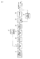
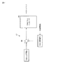
図1は、上述した連系インバータに適用可能なこの発明の一実施の形態に係るコンバータ部の回路構成を示している。 FIG. 1 shows a circuit configuration of a converter unit according to an embodiment of the present invention that can be applied to the above-described interconnected inverter.
図1に示すコンバータ部は、高周波絶縁型のDC−DCコンバータであって、出力に変動を伴う直流電源3からの電圧が入力される電圧共振回路11を備えている。この電圧共振回路11からは、高周波の電圧が出力され、この高周波電圧が高周波トランス12の1次側に入力される。高周波トランス12の二次側には、電流共振回路13が配置され、高周波トランス12から供給される電流がこの電流共振回路13で電流共振される。電流共振回路13の出力電圧は、倍電圧整流回路14に与えられ、倍電圧整流回路14からの出力電圧がスイッチング回路15でスイッチングされることから電流共振回路13の出力電圧は、倍電圧に変換されて平滑回路16を介して出力される。従って、図1に示すコンバータ部には、出力が変動される電圧が入力され、コンバータ部からは、平滑された出力電圧が出力される。
The converter unit shown in FIG. 1 is a high-frequency insulation type DC-DC converter, and includes a
スイッチング回路15は、この平滑回路16からの出力電圧Voutに応じてスイッチング回路15を制御するパルス幅変調制御回路18(PWM制御回路:Pulse Width Modulation制御回路)を備え、出力電圧Voutに応じて安定して平滑回路15に与えられる。従って、安定した出力電圧が平滑回路16から出力される。
The
図1に示されるDC−DCコンバータでは、比較的低電圧な電源3に適用されるため、電圧共振回路11が高周波トランス12の一次側に配置され、高電圧が出力される高周波トランス12の二次側に電流共振回路13が配置されている。一次側に配置された電圧共振回路11は、FET(電界効果トランジスタ)或いはIGBT(絶縁ゲート・バイポーラトランジスタ)等のスイッチング素子を備え、スイッチング素子のソース・ドレイン間(IGBTの場合にはエミッタ・コレクタ間)にキャパシタが接続され、電圧共振回路11が電圧共振するように構成される。また、二次側に配置された電流共振回路13は、直列共振により、電流共振するように構成される。従って、高効率のDC−DCコンバータを実現することができる。
Since the DC-DC converter shown in FIG. 1 is applied to the
図1に示される電圧共振回路11は、
(1)フルブリッジ
(2)ハーフブリッジ
(3)プッシュプル
の3通りの回路構成を採用することができる。これら電圧共振回路の具体的な回路例が図2から図4に示されている。
The
(1) Full circuit (2) Half bridge (3) Push-pull Three circuit configurations can be adopted. Specific circuit examples of these voltage resonance circuits are shown in FIGS.
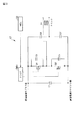
図1に示す電流共振回路13は、倍電圧整流回路14の回路構成を採用することができる。図2から図4を参照して電圧共振回路11の回路例を説明する。尚、図2から図4において、蓄電用のキャパシタC1は、通常電解コンデンサが使用されるが、各回路において共通であるので、説明を省略する。また、スイッチング素子として、FETを用いた場合を説明する。
The
図2は、フルブリッジ回路で電圧共振回路11を構成した第1の回路例を示している。図2に示す電圧共振回路においては、蓄電用のキャパシタC1が直流電源のプラス及びマイナス側の間に接続され、スイッチング素子Q1及びスイッチング素子Q2が直列接続され、スイッチング素子Q3及びスイッチング素子Q4が直列接続されている。スイッチング素子Q1〜Q4には、キャパシタC2〜C5が夫々スイッチング素子Q1〜Q4のソース・ドレイン間に並列に接続されている。また、スイッチング素子Q1、Q2の直列回路及びスイッチング素子Q3,Q4の直列回路がフルブリッジ回路を構成するように夫々入力側の直流電源に並列接続されている。従って、フルブリッジ回路とキャパシタC1とは、直流電源に並列接続されている。即ち、スイッチング素子Q1、Q3のドレインが電源のプラス側に接続され、スイッチング素子Q2、Q4のソースが電源のマイナス側に接続されている。また、スイッチング素子Q1及びスイッチング素子Q2間の接続部が出力側のトランスT1の一端部に接続され、スイッチング素子Q3及びスイッチング素子Q4の接続部がトランスT1の他端部に接続されている。
FIG. 2 shows a first circuit example in which the
図2に示すフルブリッジ回路には、スイッチング素子Q1〜Q4を所定のタイミングでオン・オフするためにスイッチング制御部17が設けられている。このスイッチング制御部17は、ドライバDR1、DR2、MCU(マイクロコントロールユニット)18から構成されている。このスイッチング制御部17においては、電流共振回路に適する周波数のゲートパルスをスイッチング素子Q1〜Q4に与えている。
In the full bridge circuit shown in FIG. 2, a switching
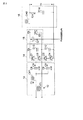
図3は、ハーフブリッジ回路で電圧共振回路11を構成した第2の回路例を示している。図3においては、図2と同一回路部品及び同一部分には、同一符号を付している。
FIG. 3 shows a second circuit example in which the
図3に示す電圧共振回路おいては、スイッチング素子Q1及びスイッチング素子Q2が直列接続され、スイッチング素子Q1、Q2には、キャパシタC2、C3がそれぞれスイッチング素子のソース・ドレイン間に並列に接続されている。また、スイッチング素子Q1、Q2の直列回路には、直列接続されたキャパシタC6,C7が並列接続されてハーフブリッジ回路を構成している。 In the voltage resonance circuit shown in FIG. 3, a switching element Q1 and a switching element Q2 are connected in series, and capacitors C2 and C3 are connected in parallel between the source and drain of the switching element, respectively. Yes. In addition, in the series circuit of the switching elements Q1 and Q2, capacitors C6 and C7 connected in series are connected in parallel to form a half bridge circuit.
そして、スイッチング素子Q1及びスイッチング素子Q2の接続部がトランスT1の一端部に接続され、キャパシタC6及びキャパシタC7の接続部がトランスT1の他端部に接続されている。 A connection portion between the switching elements Q1 and Q2 is connected to one end portion of the transformer T1, and a connection portion between the capacitors C6 and C7 is connected to the other end portion of the transformer T1.
図3に示すハーフブリッジ回路には、スイッチング素子Q1、Q2を所定のタイミングでオン・オフするために、ドライバDR1が設けられている。同様に、電流共振回路に適する周波数のゲートパルスがスイッチング素子Q1、Q2に与えられている。 In the half bridge circuit shown in FIG. 3, a driver DR1 is provided to turn on and off the switching elements Q1 and Q2 at a predetermined timing. Similarly, a gate pulse having a frequency suitable for the current resonance circuit is applied to the switching elements Q1 and Q2.
図4は、プッシュプル型で電圧共振回路11を構成した第3の回路例を示している。図4は、プッシュプル型の電圧共振回路を示している。図4においては、図2と同一回路部品及び同一部分には、同一符号を付している。
FIG. 4 shows a third circuit example in which the
図4において、スイッチング素子Q1のドレインがトランスT1の一端部に接続され、スイッチング素子Q2のドレインがトランスT1の他端部に接続され、スイッチング素子Q1、Q2のソースは、直流電源のマイナス側に接続されている。また、直流電源のプラス側は、トランスT1の一端部と他端部の中間部に接続されている。 In FIG. 4, the drain of the switching element Q1 is connected to one end of the transformer T1, the drain of the switching element Q2 is connected to the other end of the transformer T1, and the sources of the switching elements Q1 and Q2 are connected to the negative side of the DC power supply. It is connected. Further, the positive side of the DC power supply is connected to an intermediate portion between one end and the other end of the transformer T1.
図4に示すプッシュプル型で電圧共振回路11には、スイッチング素子Q1、Q2を所定のタイミングでオン・オフするために、ドライバDR1が設けられている。スイッチング素子Q1、Q2には、同様に、電流共振回路に適する周波数のゲートパルスが与えられている。
The push-pull type
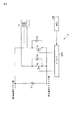
図1に示される電流共振回路13、倍電圧整流回路14、スイッチング回路15及び平滑回路16は、一例として図5に示すように構成される。図5に示す回路では、高周波トランス12の2次側の高電圧端子にチョークコイルCH1が接続され、また、この2次側の高電圧端子は、2分岐されて夫々にキャパシタC8,C9が接続されて電流共振回路13が構成されている。即ち、高周波トランス12の2次側の高電圧端子には、チョークコイルCH1及びキャパシタC8から構成される第1の直列共振回路及びチョークコイルCH1及びキャパシタC9から構成される第2の直列共振回路が接続されている。
The
この第1及び第2の直列共振回路は、倍電圧整流回路14を構成するダイオードD1、D2間の接続点及びダイオードD3、D4間の接続点に夫々接続されている。倍電圧整流回路14では、ダイオードD1、D2の直列回路にダイオードD3、D4の直列回路が接続され、両直列回路間に高周波トランス12の2次側の低電圧端子が接続されている。また、ダイオードD1、D2の直列回路には、並列にキャパシタC10が接続され、ダイオードD3、D4の直列回路には、並列にキャパシタC12が接続されて倍電圧整流回路14が構成されている。
The first and second series resonant circuits are respectively connected to a connection point between the diodes D1 and D2 and a connection point between the diodes D3 and D4 constituting the voltage
ダイオードD1、D2の直列回路には、並列にフライホイールダイオードD5及びスイッチングトランジスタQ7の直列回路が接続されてスイッチング回路15が構成されている。このスイッチング回路15では、スイッチングトランジスタQ7がオフされると、フライホイールダイオードD5が高周波トランス12の2次側の低電圧端子に接続され、フライホイールダイオードD5のカソードから低電位がチョークコイルCH2に与えられる。これに対して、スイッチングトランジスタQ7がオンされると、キャパシタC8及びダイオードD1を介して高周波トランス12の2次側の高電圧電位がキャパシタC10に与えられる。従って、キャパシタC10、C12の直列回路には、倍電圧の電位差が生じ、フライホイールダイオードD5のカソードからは、倍電圧に相当する電位が出力される。
A series circuit of the flywheel diode D5 and the switching transistor Q7 is connected in parallel to the series circuit of the diodes D1 and D2, and the switching
フライホイールダイオードD5のカソードには、チョークコイルCH2が接続され、キャパシタC10,C12の直列回路にスイッチングトランジスタQ7を介して並列にチョークコイルCH2及びキャパシタC14の直列回路が接続されている。キャパシタC14の両側は、出力端子に接続されて平滑回路16が構成されている。即ち、図5に示す回路においては、スイッチングトランジスタQ7のオン及びオフ周期に応じて、キャパシタC10、C12の直列回路には、電位差なし及び倍電圧が交互に生じ、倍電圧の振幅を有する交流電圧が平滑回路16に印加されて平滑化された倍電圧が平滑回路16から出力される。
A choke coil CH2 is connected to the cathode of the flywheel diode D5, and a series circuit of the choke coil CH2 and the capacitor C14 is connected in parallel to the series circuit of the capacitors C10 and C12 via the switching transistor Q7. Both sides of the capacitor C14 are connected to an output terminal to constitute a smoothing
図5に示すフライホイールダイオードD5及びスイッチングトランジスタQ7の直列回路からなるスイッチング回路15は、図6に示されるようにキャパシタC12に並列に接続されても良い。即ち、図6に示す回路では、スイッチングトランジスタQ7がオフされると、フライホイールダイオードD5が高周波トランス12の2次側の低電圧端子に接続され、フライホイールダイオードD5のアノードに低電位が与えられ、ダイオードD1のアノード側も低電位に維持される。これに対して、スイッチングトランジスタQ7がオンされると、キャパシタC10,C12間の接続点の電位がキャパシタC9及びダイオードD4を介して高周波トランス12の2次側の高電圧側電位にまで上昇される。また、キャパシタC8及びダイオードD1を介して高周波トランス12の2次側の高電圧電位が更にキャパシタC10に与えられることから、キャパシタC10、C12の直列回路には、倍電圧の電位差が生じ、倍電圧に相当する電位がチョークコイルCH2に与えられる。
The switching
尚、DC−DCコンバータにおいては、図5に示されるスイッチングトランジスタQ7にPWM制御信号が与えられて出力が抑制される。 In the DC-DC converter, a PWM control signal is given to the switching transistor Q7 shown in FIG.
図2及び図8(A)〜図8(H)を参照して直流電源3が定格で出力電圧(目標電圧Vout)を発生する定格出力モードでのDC−DCコンバータの動作について説明する。無負荷モード及び小出力モードでは、各部の電圧並びに電流波形が異なるのみで定格モードでの動作と同様に動作されることからその説明は省略する。
The operation of the DC-DC converter in the rated output mode in which the
DC−DCコンバータが図示せぬスイッチを介して直流電源3に接続されると、キャパシタC1の充電が開始される。同様に、キャパシタC1に対して並列に接続されているキャパシタC2,C3の直列回路及びキャパシタC4,C5の直列回路の充電も開始される。
When the DC-DC converter is connected to the
ある時点t1で制御パルス信号がドライバ回路DR1、DR2に与えられてドライバ回路DR1、DR2が動作される。この時点t1において、制御パルス信号に同期して図8(E)に示す第1及び第4のゲート信号が高レベルから低レベルに切り替えられる。従って、図8(A)に示すように、第1及び第4のゲートパルスが与えられていたFETQ1,Q4は、オフに維持される。 At a certain time t1, a control pulse signal is given to the driver circuits DR1 and DR2, and the driver circuits DR1 and DR2 are operated. At this time t1, the first and fourth gate signals shown in FIG. 8E are switched from the high level to the low level in synchronization with the control pulse signal. Therefore, as shown in FIG. 8A, the FETs Q1 and Q4 to which the first and fourth gate pulses have been applied are kept off.
時点t1後、トランスの励磁電流によって、FETQ2,Q3のソース・ドレイン間の電圧が図8(B)に示すように低下し始め、図8(A)に示すように、FETQ1,Q4のソース・ドレイン間の電圧が上昇し始める。また、図8(C)に示すように、高周波トランスT1の一次側電圧も降下を開始する。 After the time t1, the voltage between the source and drain of the FETs Q2 and Q3 starts to decrease as shown in FIG. 8B due to the exciting current of the transformer, and as shown in FIG. The voltage across the drain begins to rise. Further, as shown in FIG. 8C, the primary side voltage of the high-frequency transformer T1 also starts to drop.
時点t1から所定時間Δtだけ経過した時点t2に達すると、FETQ2,Q3のゲートに図8(D)に示される第2及び第3のゲート信号が与えられ、そのソース・ドレイン間が図8(B)に示されるように導通され、FETQ2,Q3のソース・ドレイン間電圧がゼロに低下され、FETQ2,Q3は、オン状態に維持される。また、オフに維持されるFETQ1,Q4のソース・ドレイン間電圧は、図8(A)に示すように入力電圧に達する。従って、図8(C)に示すように高周波トランスT1の一次側電圧もある所定の電圧に達し、FETQ2,Q3に電流が供給され、そのドレイン電流が図8(F)に示すように増加される。この電流が励磁電流として高周波トランスT1の一次側に供給され、その結果、その二次側に誘起電圧が発生される。 When reaching a time point t2 after a predetermined time Δt has elapsed from the time point t1, the gates of the FETs Q2 and Q3 are supplied with the second and third gate signals shown in FIG. As shown in B), the source-drain voltage of the FETs Q2 and Q3 is reduced to zero, and the FETs Q2 and Q3 are maintained in the on state. Further, the source-drain voltages of the FETs Q1 and Q4 that are kept off reach the input voltage as shown in FIG. Therefore, as shown in FIG. 8C, the primary side voltage of the high-frequency transformer T1 also reaches a predetermined voltage, current is supplied to the FETs Q2 and Q3, and the drain current is increased as shown in FIG. 8F. The This current is supplied as an exciting current to the primary side of the high-frequency transformer T1, and as a result, an induced voltage is generated on the secondary side.
尚、高周波トランスT1の2次側に接続される電流共振回路のインピーダンスは、FETQ2,Q3がオンした直後は高いことから、FETQ2,Q3のドレイン電流はゼロから緩やかに増加される。また、時点t2〜時点t3には、この高周波トランスT1の2次側に接続される電流共振回路の共振周波数に応じて半波の正弦波となるドレイン電流が生ずることとなる。 Since the impedance of the current resonance circuit connected to the secondary side of the high frequency transformer T1 is high immediately after the FETs Q2 and Q3 are turned on, the drain currents of the FETs Q2 and Q3 are gradually increased from zero. Further, at time t2 to time t3, a drain current having a half-wave sine wave is generated according to the resonance frequency of the current resonance circuit connected to the secondary side of the high-frequency transformer T1.
時点t3において、FETQ2,Q3に与えられていた第2及び第3のゲート信号がオフされると、FETQ2,Q3がオフされ、ドレイン電流が図8(F)に示すようにゼロとなる。従って、高周波トランスT1の2次側へのエネルギーの供給が停止される。また、図8(B)に示すようにオフされたFETQ2,Q3のソース・ドレイン間電圧が次第に上昇され、図8(A)に示すようにオフされているFETQ2,Q3のソース・ドレイン間電圧が次第に上昇される。FETQ2,Q3のソース・ドレイン間電圧の上昇に伴ってこのFETQ1,Q4のソース・ドレイン間の電圧が低下する。従って、高周波トランスT1の一次側電圧も次第に低下される。 At time t3, when the second and third gate signals applied to the FETs Q2 and Q3 are turned off, the FETs Q2 and Q3 are turned off and the drain current becomes zero as shown in FIG. Accordingly, the supply of energy to the secondary side of the high-frequency transformer T1 is stopped. Further, the source-drain voltage of the FETs Q2, Q3 turned off as shown in FIG. 8B is gradually increased, and the source-drain voltage of the FETs Q2, Q3 turned off as shown in FIG. 8A. Is gradually raised. As the voltage between the source and drain of the FETs Q2 and Q3 increases, the voltage between the source and drain of the FETs Q1 and Q4 decreases. Accordingly, the primary voltage of the high-frequency transformer T1 is also gradually reduced.
時点t3から所定時間Δtだけ経過した時点t4に達すると、FETQ1、Q4のゲートに図8(E)に示される第1及び第4のゲート信号が与えられ、そのソース・ドレイン間が図8(A)に示されるように導通され、FETQ1、Q4のソース・ドレイン間電圧がゼロに低下される。時点t4から時点t5までは、FETQ1、Q4はオン状態に維持される。また、オフに維持されるFETQ2、Q3のソース・ドレイン間電圧は、図8(B)に示すように入力電圧に達する。従って、図8(C)に示すように高周波トランスT1の一次側電圧もマイナス側のある所定の電圧に達し、キャパシタC1、C2,C3から導通したFETQ2、Q3に電流が供給され、そのドレイン電流が図8(G)に示すように増加される。この電流が励磁電流として高周波トランスT1の一次側に供給され、その結果、その二次側に誘起電圧が発生される。 When reaching a time point t4 after a predetermined time Δt has elapsed from the time point t3, the gates of the FETs Q1 and Q4 are given the first and fourth gate signals shown in FIG. Conduction is performed as shown in A), and the source-drain voltages of the FETs Q1 and Q4 are reduced to zero. From time t4 to time t5, the FETs Q1 and Q4 are maintained in the on state. Further, the source-drain voltages of the FETs Q2 and Q3 that are kept off reach the input voltage as shown in FIG. 8B. Therefore, as shown in FIG. 8C, the primary voltage of the high-frequency transformer T1 also reaches a predetermined voltage on the negative side, and current is supplied from the capacitors C1, C2, and C3 to the FETs Q2 and Q3 that are conducted, and the drain current thereof. Is increased as shown in FIG. This current is supplied as an exciting current to the primary side of the high-frequency transformer T1, and as a result, an induced voltage is generated on the secondary side.
ここで、時点t3〜t4においては、FETQ1,Q4に並列に接続されているキャパシタC2,C5は、緩やかに放電され、従って、FETQ1,Q4のソース・ドレイン間電圧も緩やかに降下される。その後時点t4でFETQ1,Q4がオンされるが、スイッチングした瞬間におけるFETQ1,Q4のソース・ドレイン間電圧の変化がきわめて少なく、実質的なゼロ電圧共振スイッチング(ZVS)が実現される。 Here, from time t3 to time t4, the capacitors C2 and C5 connected in parallel to the FETs Q1 and Q4 are slowly discharged, and therefore the source-drain voltages of the FETs Q1 and Q4 are also gradually lowered. Thereafter, the FETs Q1 and Q4 are turned on at time t4, but the change in the voltage between the source and drain of the FETs Q1 and Q4 at the moment of switching is extremely small, and a substantial zero voltage resonance switching (ZVS) is realized.
時点t5からは、再び時点t1〜t4におけると同様の動作が繰り返されて高周波トランスT1の二次側に誘起電圧が発生される。ここで、時点t5,t6,t7,t8は、夫々時点t1,t2,t3,t4に相当し、対応する時点の説明を参照されたい。 From time t5, the same operation as at times t1 to t4 is repeated again to generate an induced voltage on the secondary side of the high-frequency transformer T1. Here, time points t5, t6, t7, and t8 correspond to time points t1, t2, t3, and t4, respectively, and refer to the description of the corresponding time points.
ここで、時点t5〜t6においても、FETQ1,Q4に並列に接続されているキャパシタC2,C5は、同様に緩やかに充電され、従って、FETQ1,Q4のソース・ドレイン間電圧も緩やかに上昇される。その後時点t6でFETQ2,Q3がオンされるが、スイッチングした瞬間におけるFETQ2,Q3のソース・ドレイン間電圧の変化がきわめて少なく、実質的なゼロ電圧共振スイッチング(ZVS)が実現される。 Here, from time t5 to t6, the capacitors C2 and C5 connected in parallel to the FETs Q1 and Q4 are similarly slowly charged, and accordingly, the source-drain voltages of the FETs Q1 and Q4 are also gradually increased. . Thereafter, the FETs Q2 and Q3 are turned on at the time point t6, but the change in the voltage between the source and drain of the FETs Q2 and Q3 at the moment of switching is extremely small, and a substantial zero voltage resonance switching (ZVS) is realized.
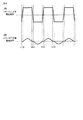
上述したように電圧共振回路が動作されることによって高周波トランスT1の2次側には、図9(A)及び9(B)に示すような電圧波形及び電流波形が出力される。即ち、図8(C)に示される高周波トランスT1の1次側の電圧波形に対応して図9(A)に示すように台形波の電圧が高周波トランスT1の2次側に現れ、また、図8(H)に示される高周波トランスT1の1次側の電流波形に対応して図9(B)に示すように正弦波の電流が高周波トランスT1の2次側に現れる。 By operating the voltage resonance circuit as described above, the voltage waveform and the current waveform as shown in FIGS. 9A and 9B are output to the secondary side of the high-frequency transformer T1. That is, a trapezoidal wave voltage appears on the secondary side of the high-frequency transformer T1, as shown in FIG. 9A, corresponding to the voltage waveform on the primary side of the high-frequency transformer T1 shown in FIG. Corresponding to the current waveform on the primary side of the high-frequency transformer T1 shown in FIG. 8H, a sinusoidal current appears on the secondary side of the high-frequency transformer T1 as shown in FIG. 9B.
図3に示すハーフブリッジ電圧共振回路11及び図4に示すプッシュプル型で電圧共振回路11についての動作は、同様にゼロ電圧共振スイッチング(ZVS)で動作され、図2のフルブリッジ電圧共振回路11の説明を参照すれば当業者であれば、容易に理解することができることからその説明は省略する。
The operation of the half-bridge
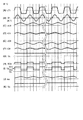
次に図5及び図10(A)〜図10(K)を参照して図5に示す回路の動作を説明する。 Next, the operation of the circuit shown in FIG. 5 will be described with reference to FIGS. 5 and 10A to 10K.
尚、図6に示される回路も図5に示す回路と略同様に動作されることから、その説明は省略する。 The circuit shown in FIG. 6 is also operated in substantially the same manner as the circuit shown in FIG.
トランス12の2次側に図10(A)及び10(B)に示すような電圧VT1及び電流iT1が発生されると、電流iT1がチョークコイルCH1に電流iL1として流入し、チョークコイルCH1を介してキャパシタC8,C9に供給される。従って、キャパシタC8,C9の両端には、夫々図10(C)及び図10(E)に示すような交流電圧vC8、vC9が生じるとともにキャパシタC8,C9からは、夫々図10(D)及び図10(F)に示すような交流電流iC8、iC9がダイオードD1、D2の接続点及びダイオードD3、D4の接続点に供給される。ダイオードD1を介してキャパシタC10が電流iC8で充電されるとともにダイオードD3を介してキャパシタC12が電流iC9で充電される。従って、ダイオードD1の電位が図10(G)に示すように電位Vaに維持される。ここで、電位Vaは、キャパシタC10、C12間の電位にキャパシタC10の電圧を加算した実質的な4倍電圧に相当している。
When the voltage VT1 and the current iT1 as shown in FIGS. 10A and 10B are generated on the secondary side of the
図10(H)に示すようにスイッチング素子Q7にPWM制御信号としてスイッチング信号SQ1が与えられると、スイッチング素子Q7がオン及びオフに応じて、電位VbがフライホイールダイオードD5のアノードに生ずる。スイッチング素子Q7がオフの際には、電位Vaがスイッチング素子SQ7を介してフライホイールダイオードD5のカソードに与えられず、図10(I)に示すようにキャパシタC10及びC12間の電位Vb2に対応した電位VbがフライホイールダイオードD5のアノードに生ずる。これに対して、スイッチング素子Q7がオンの際には、電位Vaがスイッチング素子SQ7を介してフライホイールダイオードD5のカソードに与えられ、図10(I)に示すように電位Vaに対応した電位Vb1がフライホイールダイオードD5のカソードに与えられる。従って、フライホイールダイオードD5のカソード側の電位Vbは、スイッチング素子Q7のオン及びオフに応じて、電位VOUTを基準として電位Vb1及び電位Vb2間で矩形波として変動される。図10(I)に示される矩形波電位Vbは、チョークコイルCH2及びキャパシタC14から成る平滑回路16に与えられる。従って、図10(J)に示されるようにこの平滑回路では、平滑電流iC0でキャパシタC14が充電され、図10(K)に示される出力電圧VOUTがキャパシタC14の両端電圧として出力される。
As shown in FIG. 10 (H), when the switching signal SQ1 is given as the PWM control signal to the switching element Q7, the potential Vb is generated at the anode of the flywheel diode D5 in accordance with the switching element Q7 being turned on and off. When the switching element Q7 is off, the potential Va is not applied to the cathode of the flywheel diode D5 via the switching element SQ7, and corresponds to the potential Vb2 between the capacitors C10 and C12 as shown in FIG. 10 (I). A potential Vb is generated at the anode of the flywheel diode D5. On the other hand, when switching element Q7 is on, potential Va is applied to the cathode of flywheel diode D5 via switching element SQ7, and potential Vb1 corresponding to potential Va as shown in FIG. 10 (I). Is applied to the cathode of the flywheel diode D5. Therefore, the potential Vb on the cathode side of the flywheel diode D5 varies as a rectangular wave between the potential Vb1 and the potential Vb2 with reference to the potential VOUT in accordance with the on / off of the switching element Q7. The rectangular wave potential Vb shown in FIG. 10 (I) is applied to the smoothing
尚、キャパシタC8、C9は、チョークコイルCH1とで共振回路を構成すると、同時にチャージポンプとして働き、倍電圧整流を実現している。この時、電圧Vaは、次のように示すことができる。 When the capacitors C8 and C9 form a resonance circuit with the choke coil CH1, the capacitors C8 and C9 simultaneously function as a charge pump to realize voltage doubler rectification. At this time, the voltage Va can be expressed as follows.
Va=2×vT10+2×vT12
vT10は、高周波トランス12の正端子電圧であり、vT12は、高周波トランス12の負端子電圧である。
Va = 2 × vT10 + 2 × vT12
vT10 is a positive terminal voltage of the high-
PWM制御において、スイッチング素子Q7をオンとするデューティをdとすると、出力電圧VOUTは次式にて示すことができる。 In PWM control, if the duty for turning on the switching element Q7 is d, the output voltage VOUT can be expressed by the following equation.
VOUT=2×vT10×d+2×vT12
上述したコンバータ回路においては、PWM信号のパルス幅に応じて図10(K)に示されるように平滑回路16からは平滑化された出力電圧VOUTが出力される。ここで、PWM信号のパルス幅が大きければ、平滑回路16からの出力電圧VOUTが大きくなり、PWM信号のパルス幅が小さければ、平滑回路16からの出力電圧VOUTが小さくなる。従って、平滑回路16からの出力電圧がPWM信号発生器18で検出され、適切なパルス幅が選定されることによって平滑回路16の出力を一定とすることができる。
VOUT = 2 × vT10 × d + 2 × vT12
In the converter circuit described above, the smoothed output voltage VOUT is output from the smoothing
図5に示す回路では、トランスの2次側には、2回路ではなく、単一回路が設けられるのみで構成されている。通常、1つのトランスにおいて、2次側に2回路の2次巻き線を施した場合、リーケージインダクタンスの差により、共振周波数のずれが生じてしまう。このリーケージインダクタンスの差を極力少なくするには2個のトランスを必要とする。しかし、トランスの2次側が単一回路で構成されることから、小出力時においても高い変換効率を有するDC−DCコンバータを提供することができる。 In the circuit shown in FIG. 5, only a single circuit is provided on the secondary side of the transformer instead of two circuits. Normally, when two secondary windings are provided on the secondary side in one transformer, the resonance frequency shifts due to a difference in leakage inductance. Two transformers are required to minimize the difference in leakage inductance. However, since the secondary side of the transformer is composed of a single circuit, it is possible to provide a DC-DC converter having high conversion efficiency even at a small output.
以上のように,定格出力時はもちろんのこと、小出力時においても高い変換効率を有するDC−DCコンバータを提供することができる。 As described above, it is possible to provide a DC-DC converter having high conversion efficiency not only at the rated output but also at the small output.
この発明は、上記各実施の形態に限ることなく、その他、実施段階ではその要旨を逸脱しない範囲で種々の変形を実施し得ることが可能である。さらに、上記各実施形態には、種々の段階の発明が含まれており、開示される複数の構成要件における適宜な組合せにより種々の発明が抽出され得る。 The present invention is not limited to the above-described embodiments, and various modifications can be made without departing from the spirit of the invention at the stage of implementation. Further, the above embodiments include inventions at various stages, and various inventions can be extracted by appropriately combining a plurality of disclosed constituent elements.
また、例えば各実施形態に示される全構成要件から幾つかの構成要件が削除されても、発明が解決しようとする課題の欄で述べた課題が解決でき、発明の効果で述べられている効果が得られる場合には、この構成要件が削除された構成が発明として抽出され得る。 In addition, for example, even if some structural requirements are deleted from all the structural requirements shown in each embodiment, the problem described in the column of the problem to be solved by the invention can be solved, and the effect described in the effect of the invention Can be obtained as an invention.
C1〜C14…キャパシタ、Q1〜Q7…スイッチング素子、DR1、DR2…ドライバ、D1〜D5…ダイオード、CH1、CH2…チョークコイル、11…電圧共振回路、12…高周波トランス、13…電流共振回路、14…整流回路、15…スイッチング回路、16…平滑回路、18・・・PWM制御回路、17…スイッチング制御回路 C1 to C14 ... capacitors, Q1 to Q7 ... switching elements, DR1, DR2 ... drivers, D1 to D5 ... diodes, CH1, CH2 ... choke coils, 11 ... voltage resonance circuit, 12 ... high frequency transformer, 13 ... current resonance circuit, 14 Rectifier circuit, 15 switching circuit, 16 smoothing circuit, 18 PWM control circuit, 17 switching control circuit
Claims (4)
1次側及び2次側を有し、その1次側に前記第1の電圧共振回路からの出力電圧が入力される第1の絶縁型高周波トランスと、
前記第1のトランスの2次側の第1端子に接続されるチョークコイル及びこのチョークコイルに夫々直列に接続される第1及び第2キャパシタから成る第1の電流共振回路と、
第1及び第2のダイオードが直列接続された第1のダイオード接続、この第1のダイオード接続に並列に接続された第3キャパシタ、第2及び第3のダイオードが直列接続された第2のダイオード接続、この第2のダイオード接続に並列に接続された第4キャパシタとから構成され、この第1及び第2のダイオード接続間の接続点並びに第3及び第4のキャパシタ間の接続点が前記第1のトランスの2次側の第2端子に接続され、前記第3キャパシタが前記第1及び第2のダイオード間の接続点に接続され、前記第4キャパシタが前記第3及び第4のダイオード間の接続点に接続されている倍電圧回路と、
前記第3及び第4キャパシタの一方の電圧或いは前記第3及び第4キャパシタの直列接続の電圧を切り替えるスイッチング回路と、
このスイッチング回路からの出力を平滑化して出力する平滑回路と、
を具備することを特徴とするDC―DCコンバータ。 A first voltage resonance circuit that receives DC power from a low-voltage DC power supply whose output voltage fluctuates, performs DC-AC conversion, and outputs;
A first insulated high-frequency transformer having a primary side and a secondary side, into which an output voltage from the first voltage resonance circuit is input;
A first current resonance circuit comprising a choke coil connected to the first terminal on the secondary side of the first transformer and first and second capacitors connected in series to the choke coil;
A first diode connection in which the first and second diodes are connected in series, a third capacitor connected in parallel to the first diode connection, and a second diode in which the second and third diodes are connected in series And a fourth capacitor connected in parallel to the second diode connection, and a connection point between the first and second diode connections and a connection point between the third and fourth capacitors are the first and second capacitors. Connected to a second terminal on the secondary side of one transformer, the third capacitor is connected to a connection point between the first and second diodes, and the fourth capacitor is connected between the third and fourth diodes. A voltage doubler connected to the connection point of
A switching circuit for switching one voltage of the third and fourth capacitors or a voltage in series connection of the third and fourth capacitors;
A smoothing circuit for smoothing and outputting the output from the switching circuit;
A DC-DC converter comprising:
Priority Applications (1)
| Application Number | Priority Date | Filing Date | Title |
|---|---|---|---|
| JP2006039418A JP2007221915A (en) | 2006-02-16 | 2006-02-16 | Dc-dc converter |
Applications Claiming Priority (1)
| Application Number | Priority Date | Filing Date | Title |
|---|---|---|---|
| JP2006039418A JP2007221915A (en) | 2006-02-16 | 2006-02-16 | Dc-dc converter |
Publications (2)
| Publication Number | Publication Date |
|---|---|
| JP2007221915A true JP2007221915A (en) | 2007-08-30 |
| JP2007221915A5 JP2007221915A5 (en) | 2009-06-04 |
Family
ID=38498550
Family Applications (1)
| Application Number | Title | Priority Date | Filing Date |
|---|---|---|---|
| JP2006039418A Pending JP2007221915A (en) | 2006-02-16 | 2006-02-16 | Dc-dc converter |
Country Status (1)
| Country | Link |
|---|---|
| JP (1) | JP2007221915A (en) |
Cited By (9)
| Publication number | Priority date | Publication date | Assignee | Title |
|---|---|---|---|---|
| JP2010158150A (en) * | 2008-12-30 | 2010-07-15 | Internatl Business Mach Corp <Ibm> | Apparatus, system, method and power supply mechanism for providing efficient multiple power outputs (apparatus, system, and method for asynchronous multiple output power supply mechanism) |
| JP2011120370A (en) * | 2009-12-03 | 2011-06-16 | Origin Electric Co Ltd | Dc-dc bidirectional converter circuit |
| WO2012144249A1 (en) * | 2011-04-18 | 2012-10-26 | 三菱電機株式会社 | Power conversion device and in-vehicle power supply device equipped with same |
| WO2013132727A1 (en) * | 2012-03-05 | 2013-09-12 | 富士電機株式会社 | Dc-dc conversion device |
| WO2013132726A1 (en) * | 2012-03-05 | 2013-09-12 | 富士電機株式会社 | Dc-dc conversion device |
| WO2014002291A1 (en) * | 2012-06-29 | 2014-01-03 | 日立オートモティブシステムズ阪神株式会社 | Ignition device for internal combustion engine |
| WO2014006762A1 (en) * | 2012-07-03 | 2014-01-09 | 日立オートモティブシステムズ阪神株式会社 | Ignition device for internal combustion engine |
| JP2014506111A (en) * | 2010-12-29 | 2014-03-06 | 日本テキサス・インスツルメンツ株式会社 | System for wireless power transmission |
| JP2015228760A (en) * | 2014-06-02 | 2015-12-17 | 京都電機器株式会社 | Switching power supply |
Citations (2)
| Publication number | Priority date | Publication date | Assignee | Title |
|---|---|---|---|---|
| JP2004254393A (en) * | 2003-02-19 | 2004-09-09 | Tdk Corp | Switching power supply unit |
| JP2005304289A (en) * | 2004-03-18 | 2005-10-27 | Mitsui & Co Ltd | Dc-dc converter |
-
2006
- 2006-02-16 JP JP2006039418A patent/JP2007221915A/en active Pending
Patent Citations (2)
| Publication number | Priority date | Publication date | Assignee | Title |
|---|---|---|---|---|
| JP2004254393A (en) * | 2003-02-19 | 2004-09-09 | Tdk Corp | Switching power supply unit |
| JP2005304289A (en) * | 2004-03-18 | 2005-10-27 | Mitsui & Co Ltd | Dc-dc converter |
Cited By (17)
| Publication number | Priority date | Publication date | Assignee | Title |
|---|---|---|---|---|
| JP2010158150A (en) * | 2008-12-30 | 2010-07-15 | Internatl Business Mach Corp <Ibm> | Apparatus, system, method and power supply mechanism for providing efficient multiple power outputs (apparatus, system, and method for asynchronous multiple output power supply mechanism) |
| JP2011120370A (en) * | 2009-12-03 | 2011-06-16 | Origin Electric Co Ltd | Dc-dc bidirectional converter circuit |
| JP2014506111A (en) * | 2010-12-29 | 2014-03-06 | 日本テキサス・インスツルメンツ株式会社 | System for wireless power transmission |
| JP5558631B2 (en) * | 2011-04-18 | 2014-07-23 | 三菱電機株式会社 | Power conversion device and in-vehicle power supply device including the same |
| WO2012144249A1 (en) * | 2011-04-18 | 2012-10-26 | 三菱電機株式会社 | Power conversion device and in-vehicle power supply device equipped with same |
| US9787190B2 (en) | 2011-04-18 | 2017-10-10 | Mitsubishi Electric Corporation | Power conversion device and in-vehicle power supply device equipped with same |
| CN103503292B (en) * | 2011-04-18 | 2016-04-20 | 三菱电机株式会社 | Power-converting device and possess the vehicular electric power source device of this power-converting device |
| CN103503292A (en) * | 2011-04-18 | 2014-01-08 | 三菱电机株式会社 | Power conversion device and in-vehicle power supply device equipped with same |
| JPWO2012144249A1 (en) * | 2011-04-18 | 2014-07-28 | 三菱電機株式会社 | Power conversion device and in-vehicle power supply device including the same |
| WO2013132726A1 (en) * | 2012-03-05 | 2013-09-12 | 富士電機株式会社 | Dc-dc conversion device |
| CN104115386A (en) * | 2012-03-05 | 2014-10-22 | 富士电机株式会社 | DC-DC conversion device |
| US9350255B2 (en) | 2012-03-05 | 2016-05-24 | Fuji Electric Co., Ltd. | DC-DC conversion device including pulse width modulation control |
| WO2013132727A1 (en) * | 2012-03-05 | 2013-09-12 | 富士電機株式会社 | Dc-dc conversion device |
| WO2014002291A1 (en) * | 2012-06-29 | 2014-01-03 | 日立オートモティブシステムズ阪神株式会社 | Ignition device for internal combustion engine |
| WO2014006762A1 (en) * | 2012-07-03 | 2014-01-09 | 日立オートモティブシステムズ阪神株式会社 | Ignition device for internal combustion engine |
| JP5750813B2 (en) * | 2012-07-03 | 2015-07-22 | 日立オートモティブシステムズ阪神株式会社 | Ignition device for internal combustion engine |
| JP2015228760A (en) * | 2014-06-02 | 2015-12-17 | 京都電機器株式会社 | Switching power supply |
Similar Documents
| Publication | Publication Date | Title |
|---|---|---|
| US7333348B2 (en) | DC-DC converter | |
| Chen et al. | Study and implementation of a current-fed full-bridge boost DC–DC converter with zero-current switching for high-voltage applications | |
| Gui et al. | A high voltage-gain LLC micro-converter with high efficiency in wide input range for PV applications | |
| JP2007221915A (en) | Dc-dc converter | |
| JP3344356B2 (en) | Switching power supply | |
| WO2010107060A1 (en) | Dc-dc converter | |
| JP2012050264A (en) | Load driving device | |
| CN110707930A (en) | DC/DC converter | |
| JP5424307B2 (en) | Isolated DC-DC converter | |
| Zhang et al. | A dual coupled inductors-based high step-up/step-down bidirectional dc-dc converter for energy storage system | |
| JP2009060747A (en) | Dc-dc converter | |
| WO2010098486A1 (en) | Dc-dc converter | |
| CN113541503A (en) | Zero-current switch active clamping current type push-pull direct-current converter | |
| JP5457204B2 (en) | Full bridge composite resonance type DC-DC converter | |
| JP3934654B2 (en) | DC-DC converter | |
| KR20060042996A (en) | Discharge lamp lighting apparatus | |
| KR100941935B1 (en) | Three phase interleaved isolated dc/dc converter | |
| JP2005304289A (en) | Dc-dc converter | |
| JP2001197737A (en) | High voltage power supply circuit | |
| Ekkaravarodome et al. | Analysis and implementation of a half bridge Class-DE rectifier for front-end ZVS push-pull resonant converters | |
| Yang | Novel dual DC-DC flyback converter with leakage-energy recycling | |
| Moradisizkoohi et al. | Ultra-high step-up DC/DC converter based on dual-coupled-inductors with low voltage stress and input current ripple for renewable energy applications | |
| JP5500438B2 (en) | Load drive device | |
| KR101704189B1 (en) | Ozone Generation Power Supply | |
| Lee et al. | Three-level LLC SRC for high and wide input voltage applications |
Legal Events
| Date | Code | Title | Description |
|---|---|---|---|
| A521 | Written amendment |
Effective date: 20081224 Free format text: JAPANESE INTERMEDIATE CODE: A523 |
|
| A621 | Written request for application examination |
Effective date: 20081224 Free format text: JAPANESE INTERMEDIATE CODE: A621 |
|
| A521 | Written amendment |
Effective date: 20090420 Free format text: JAPANESE INTERMEDIATE CODE: A523 |
|
| A711 | Notification of change in applicant |
Free format text: JAPANESE INTERMEDIATE CODE: A711 Effective date: 20100421 |
|
| A521 | Written amendment |
Effective date: 20100421 Free format text: JAPANESE INTERMEDIATE CODE: A821 |
|
| A521 | Written amendment |
Free format text: JAPANESE INTERMEDIATE CODE: A523 Effective date: 20100623 |
|
| A521 | Written amendment |
Free format text: JAPANESE INTERMEDIATE CODE: A821 Effective date: 20100623 |
|
| A977 | Report on retrieval |
Effective date: 20110617 Free format text: JAPANESE INTERMEDIATE CODE: A971007 |
|
| A131 | Notification of reasons for refusal |
Effective date: 20110802 Free format text: JAPANESE INTERMEDIATE CODE: A131 |
|
| A02 | Decision of refusal |
Effective date: 20111129 Free format text: JAPANESE INTERMEDIATE CODE: A02 |