JPWO2005096683A1 - Circuit board, manufacturing method thereof, and joint box using circuit board - Google Patents
Circuit board, manufacturing method thereof, and joint box using circuit board Download PDFInfo
- Publication number
- JPWO2005096683A1 JPWO2005096683A1 JP2006511657A JP2006511657A JPWO2005096683A1 JP WO2005096683 A1 JPWO2005096683 A1 JP WO2005096683A1 JP 2006511657 A JP2006511657 A JP 2006511657A JP 2006511657 A JP2006511657 A JP 2006511657A JP WO2005096683 A1 JPWO2005096683 A1 JP WO2005096683A1
- Authority
- JP
- Japan
- Prior art keywords
- circuit board
- circuit
- terminal
- resin plate
- circuit pattern
- Prior art date
- Legal status (The legal status is an assumption and is not a legal conclusion. Google has not performed a legal analysis and makes no representation as to the accuracy of the status listed.)
- Pending
Links
Images


Classifications
-
- H—ELECTRICITY
- H05—ELECTRIC TECHNIQUES NOT OTHERWISE PROVIDED FOR
- H05K—PRINTED CIRCUITS; CASINGS OR CONSTRUCTIONAL DETAILS OF ELECTRIC APPARATUS; MANUFACTURE OF ASSEMBLAGES OF ELECTRICAL COMPONENTS
- H05K3/00—Apparatus or processes for manufacturing printed circuits
- H05K3/10—Apparatus or processes for manufacturing printed circuits in which conductive material is applied to the insulating support in such a manner as to form the desired conductive pattern
- H05K3/20—Apparatus or processes for manufacturing printed circuits in which conductive material is applied to the insulating support in such a manner as to form the desired conductive pattern by affixing prefabricated conductor pattern
- H05K3/202—Apparatus or processes for manufacturing printed circuits in which conductive material is applied to the insulating support in such a manner as to form the desired conductive pattern by affixing prefabricated conductor pattern using self-supporting metal foil pattern
-
- H—ELECTRICITY
- H02—GENERATION; CONVERSION OR DISTRIBUTION OF ELECTRIC POWER
- H02G—INSTALLATION OF ELECTRIC CABLES OR LINES, OR OF COMBINED OPTICAL AND ELECTRIC CABLES OR LINES
- H02G3/00—Installations of electric cables or lines or protective tubing therefor in or on buildings, equivalent structures or vehicles
- H02G3/02—Details
- H02G3/08—Distribution boxes; Connection or junction boxes
-
- H—ELECTRICITY
- H01—ELECTRIC ELEMENTS
- H01R—ELECTRICALLY-CONDUCTIVE CONNECTIONS; STRUCTURAL ASSOCIATIONS OF A PLURALITY OF MUTUALLY-INSULATED ELECTRICAL CONNECTING ELEMENTS; COUPLING DEVICES; CURRENT COLLECTORS
- H01R12/00—Structural associations of a plurality of mutually-insulated electrical connecting elements, specially adapted for printed circuits, e.g. printed circuit boards [PCB], flat or ribbon cables, or like generally planar structures, e.g. terminal strips, terminal blocks; Coupling devices specially adapted for printed circuits, flat or ribbon cables, or like generally planar structures; Terminals specially adapted for contact with, or insertion into, printed circuits, flat or ribbon cables, or like generally planar structures
- H01R12/50—Fixed connections
- H01R12/51—Fixed connections for rigid printed circuits or like structures
- H01R12/52—Fixed connections for rigid printed circuits or like structures connecting to other rigid printed circuits or like structures
- H01R12/523—Fixed connections for rigid printed circuits or like structures connecting to other rigid printed circuits or like structures by an interconnection through aligned holes in the boards or multilayer board
-
- H—ELECTRICITY
- H01—ELECTRIC ELEMENTS
- H01R—ELECTRICALLY-CONDUCTIVE CONNECTIONS; STRUCTURAL ASSOCIATIONS OF A PLURALITY OF MUTUALLY-INSULATED ELECTRICAL CONNECTING ELEMENTS; COUPLING DEVICES; CURRENT COLLECTORS
- H01R9/00—Structural associations of a plurality of mutually-insulated electrical connecting elements, e.g. terminal strips or terminal blocks; Terminals or binding posts mounted upon a base or in a case; Bases therefor
- H01R9/22—Bases, e.g. strip, block, panel
- H01R9/24—Terminal blocks
- H01R9/2458—Electrical interconnections between terminal blocks
- H01R9/2466—Electrical interconnections between terminal blocks using a planar conductive structure, e.g. printed circuit board
-
- H—ELECTRICITY
- H02—GENERATION; CONVERSION OR DISTRIBUTION OF ELECTRIC POWER
- H02G—INSTALLATION OF ELECTRIC CABLES OR LINES, OR OF COMBINED OPTICAL AND ELECTRIC CABLES OR LINES
- H02G3/00—Installations of electric cables or lines or protective tubing therefor in or on buildings, equivalent structures or vehicles
- H02G3/02—Details
- H02G3/08—Distribution boxes; Connection or junction boxes
- H02G3/16—Distribution boxes; Connection or junction boxes structurally associated with support for line-connecting terminals within the box
-
- H—ELECTRICITY
- H05—ELECTRIC TECHNIQUES NOT OTHERWISE PROVIDED FOR
- H05K—PRINTED CIRCUITS; CASINGS OR CONSTRUCTIONAL DETAILS OF ELECTRIC APPARATUS; MANUFACTURE OF ASSEMBLAGES OF ELECTRICAL COMPONENTS
- H05K1/00—Printed circuits
- H05K1/02—Details
-
- H—ELECTRICITY
- H05—ELECTRIC TECHNIQUES NOT OTHERWISE PROVIDED FOR
- H05K—PRINTED CIRCUITS; CASINGS OR CONSTRUCTIONAL DETAILS OF ELECTRIC APPARATUS; MANUFACTURE OF ASSEMBLAGES OF ELECTRICAL COMPONENTS
- H05K13/00—Apparatus or processes specially adapted for manufacturing or adjusting assemblages of electric components
- H05K13/0061—Tools for holding the circuit boards during processing; handling transport of printed circuit boards
-
- H—ELECTRICITY
- H05—ELECTRIC TECHNIQUES NOT OTHERWISE PROVIDED FOR
- H05K—PRINTED CIRCUITS; CASINGS OR CONSTRUCTIONAL DETAILS OF ELECTRIC APPARATUS; MANUFACTURE OF ASSEMBLAGES OF ELECTRICAL COMPONENTS
- H05K3/00—Apparatus or processes for manufacturing printed circuits
- H05K3/02—Apparatus or processes for manufacturing printed circuits in which the conductive material is applied to the surface of the insulating support and is thereafter removed from such areas of the surface which are not intended for current conducting or shielding
- H05K3/04—Apparatus or processes for manufacturing printed circuits in which the conductive material is applied to the surface of the insulating support and is thereafter removed from such areas of the surface which are not intended for current conducting or shielding the conductive material being removed mechanically, e.g. by punching
- H05K3/041—Apparatus or processes for manufacturing printed circuits in which the conductive material is applied to the surface of the insulating support and is thereafter removed from such areas of the surface which are not intended for current conducting or shielding the conductive material being removed mechanically, e.g. by punching by using a die for cutting the conductive material
-
- H—ELECTRICITY
- H05—ELECTRIC TECHNIQUES NOT OTHERWISE PROVIDED FOR
- H05K—PRINTED CIRCUITS; CASINGS OR CONSTRUCTIONAL DETAILS OF ELECTRIC APPARATUS; MANUFACTURE OF ASSEMBLAGES OF ELECTRICAL COMPONENTS
- H05K3/00—Apparatus or processes for manufacturing printed circuits
- H05K3/10—Apparatus or processes for manufacturing printed circuits in which conductive material is applied to the insulating support in such a manner as to form the desired conductive pattern
- H05K3/20—Apparatus or processes for manufacturing printed circuits in which conductive material is applied to the insulating support in such a manner as to form the desired conductive pattern by affixing prefabricated conductor pattern
-
- H—ELECTRICITY
- H05—ELECTRIC TECHNIQUES NOT OTHERWISE PROVIDED FOR
- H05K—PRINTED CIRCUITS; CASINGS OR CONSTRUCTIONAL DETAILS OF ELECTRIC APPARATUS; MANUFACTURE OF ASSEMBLAGES OF ELECTRICAL COMPONENTS
- H05K2201/00—Indexing scheme relating to printed circuits covered by H05K1/00
- H05K2201/03—Conductive materials
- H05K2201/0332—Structure of the conductor
- H05K2201/0364—Conductor shape
- H05K2201/0376—Flush conductors, i.e. flush with the surface of the printed circuit
-
- H—ELECTRICITY
- H05—ELECTRIC TECHNIQUES NOT OTHERWISE PROVIDED FOR
- H05K—PRINTED CIRCUITS; CASINGS OR CONSTRUCTIONAL DETAILS OF ELECTRIC APPARATUS; MANUFACTURE OF ASSEMBLAGES OF ELECTRICAL COMPONENTS
- H05K2201/00—Indexing scheme relating to printed circuits covered by H05K1/00
- H05K2201/03—Conductive materials
- H05K2201/0332—Structure of the conductor
- H05K2201/0388—Other aspects of conductors
- H05K2201/0394—Conductor crossing over a hole in the substrate or a gap between two separate substrate parts
-
- H—ELECTRICITY
- H05—ELECTRIC TECHNIQUES NOT OTHERWISE PROVIDED FOR
- H05K—PRINTED CIRCUITS; CASINGS OR CONSTRUCTIONAL DETAILS OF ELECTRIC APPARATUS; MANUFACTURE OF ASSEMBLAGES OF ELECTRICAL COMPONENTS
- H05K2201/00—Indexing scheme relating to printed circuits covered by H05K1/00
- H05K2201/03—Conductive materials
- H05K2201/0332—Structure of the conductor
- H05K2201/0388—Other aspects of conductors
- H05K2201/0397—Tab
-
- H—ELECTRICITY
- H05—ELECTRIC TECHNIQUES NOT OTHERWISE PROVIDED FOR
- H05K—PRINTED CIRCUITS; CASINGS OR CONSTRUCTIONAL DETAILS OF ELECTRIC APPARATUS; MANUFACTURE OF ASSEMBLAGES OF ELECTRICAL COMPONENTS
- H05K2201/00—Indexing scheme relating to printed circuits covered by H05K1/00
- H05K2201/09—Shape and layout
- H05K2201/09009—Substrate related
- H05K2201/09036—Recesses or grooves in insulating substrate
-
- H—ELECTRICITY
- H05—ELECTRIC TECHNIQUES NOT OTHERWISE PROVIDED FOR
- H05K—PRINTED CIRCUITS; CASINGS OR CONSTRUCTIONAL DETAILS OF ELECTRIC APPARATUS; MANUFACTURE OF ASSEMBLAGES OF ELECTRICAL COMPONENTS
- H05K2201/00—Indexing scheme relating to printed circuits covered by H05K1/00
- H05K2201/09—Shape and layout
- H05K2201/09009—Substrate related
- H05K2201/09045—Locally raised area or protrusion of insulating substrate
-
- H—ELECTRICITY
- H05—ELECTRIC TECHNIQUES NOT OTHERWISE PROVIDED FOR
- H05K—PRINTED CIRCUITS; CASINGS OR CONSTRUCTIONAL DETAILS OF ELECTRIC APPARATUS; MANUFACTURE OF ASSEMBLAGES OF ELECTRICAL COMPONENTS
- H05K2201/00—Indexing scheme relating to printed circuits covered by H05K1/00
- H05K2201/09—Shape and layout
- H05K2201/09009—Substrate related
- H05K2201/091—Locally and permanently deformed areas including dielectric material
-
- H—ELECTRICITY
- H05—ELECTRIC TECHNIQUES NOT OTHERWISE PROVIDED FOR
- H05K—PRINTED CIRCUITS; CASINGS OR CONSTRUCTIONAL DETAILS OF ELECTRIC APPARATUS; MANUFACTURE OF ASSEMBLAGES OF ELECTRICAL COMPONENTS
- H05K2201/00—Indexing scheme relating to printed circuits covered by H05K1/00
- H05K2201/09—Shape and layout
- H05K2201/09209—Shape and layout details of conductors
- H05K2201/095—Conductive through-holes or vias
- H05K2201/096—Vertically aligned vias, holes or stacked vias
-
- H—ELECTRICITY
- H05—ELECTRIC TECHNIQUES NOT OTHERWISE PROVIDED FOR
- H05K—PRINTED CIRCUITS; CASINGS OR CONSTRUCTIONAL DETAILS OF ELECTRIC APPARATUS; MANUFACTURE OF ASSEMBLAGES OF ELECTRICAL COMPONENTS
- H05K2201/00—Indexing scheme relating to printed circuits covered by H05K1/00
- H05K2201/10—Details of components or other objects attached to or integrated in a printed circuit board
- H05K2201/10227—Other objects, e.g. metallic pieces
- H05K2201/10287—Metal wires as connectors or conductors
-
- H—ELECTRICITY
- H05—ELECTRIC TECHNIQUES NOT OTHERWISE PROVIDED FOR
- H05K—PRINTED CIRCUITS; CASINGS OR CONSTRUCTIONAL DETAILS OF ELECTRIC APPARATUS; MANUFACTURE OF ASSEMBLAGES OF ELECTRICAL COMPONENTS
- H05K2201/00—Indexing scheme relating to printed circuits covered by H05K1/00
- H05K2201/10—Details of components or other objects attached to or integrated in a printed circuit board
- H05K2201/10227—Other objects, e.g. metallic pieces
- H05K2201/10401—Eyelets, i.e. rings inserted into a hole through a circuit board
-
- H—ELECTRICITY
- H05—ELECTRIC TECHNIQUES NOT OTHERWISE PROVIDED FOR
- H05K—PRINTED CIRCUITS; CASINGS OR CONSTRUCTIONAL DETAILS OF ELECTRIC APPARATUS; MANUFACTURE OF ASSEMBLAGES OF ELECTRICAL COMPONENTS
- H05K2201/00—Indexing scheme relating to printed circuits covered by H05K1/00
- H05K2201/10—Details of components or other objects attached to or integrated in a printed circuit board
- H05K2201/10431—Details of mounted components
- H05K2201/1059—Connections made by press-fit insertion
-
- H—ELECTRICITY
- H05—ELECTRIC TECHNIQUES NOT OTHERWISE PROVIDED FOR
- H05K—PRINTED CIRCUITS; CASINGS OR CONSTRUCTIONAL DETAILS OF ELECTRIC APPARATUS; MANUFACTURE OF ASSEMBLAGES OF ELECTRICAL COMPONENTS
- H05K2201/00—Indexing scheme relating to printed circuits covered by H05K1/00
- H05K2201/10—Details of components or other objects attached to or integrated in a printed circuit board
- H05K2201/10431—Details of mounted components
- H05K2201/10598—Means for fastening a component, a casing or a heat sink whereby a pressure is exerted on the component towards the PCB
-
- H—ELECTRICITY
- H05—ELECTRIC TECHNIQUES NOT OTHERWISE PROVIDED FOR
- H05K—PRINTED CIRCUITS; CASINGS OR CONSTRUCTIONAL DETAILS OF ELECTRIC APPARATUS; MANUFACTURE OF ASSEMBLAGES OF ELECTRICAL COMPONENTS
- H05K2203/00—Indexing scheme relating to apparatus or processes for manufacturing printed circuits covered by H05K3/00
- H05K2203/08—Treatments involving gases
- H05K2203/081—Blowing of gas, e.g. for cooling or for providing heat during solder reflowing
-
- H—ELECTRICITY
- H05—ELECTRIC TECHNIQUES NOT OTHERWISE PROVIDED FOR
- H05K—PRINTED CIRCUITS; CASINGS OR CONSTRUCTIONAL DETAILS OF ELECTRIC APPARATUS; MANUFACTURE OF ASSEMBLAGES OF ELECTRICAL COMPONENTS
- H05K2203/00—Indexing scheme relating to apparatus or processes for manufacturing printed circuits covered by H05K3/00
- H05K2203/08—Treatments involving gases
- H05K2203/082—Suction, e.g. for holding solder balls or components
-
- H—ELECTRICITY
- H05—ELECTRIC TECHNIQUES NOT OTHERWISE PROVIDED FOR
- H05K—PRINTED CIRCUITS; CASINGS OR CONSTRUCTIONAL DETAILS OF ELECTRIC APPARATUS; MANUFACTURE OF ASSEMBLAGES OF ELECTRICAL COMPONENTS
- H05K2203/00—Indexing scheme relating to apparatus or processes for manufacturing printed circuits covered by H05K3/00
- H05K2203/16—Inspection; Monitoring; Aligning
- H05K2203/167—Using mechanical means for positioning, alignment or registration, e.g. using rod-in-hole alignment
-
- H—ELECTRICITY
- H05—ELECTRIC TECHNIQUES NOT OTHERWISE PROVIDED FOR
- H05K—PRINTED CIRCUITS; CASINGS OR CONSTRUCTIONAL DETAILS OF ELECTRIC APPARATUS; MANUFACTURE OF ASSEMBLAGES OF ELECTRICAL COMPONENTS
- H05K3/00—Apparatus or processes for manufacturing printed circuits
- H05K3/22—Secondary treatment of printed circuits
- H05K3/222—Completing of printed circuits by adding non-printed jumper connections
-
- H—ELECTRICITY
- H05—ELECTRIC TECHNIQUES NOT OTHERWISE PROVIDED FOR
- H05K—PRINTED CIRCUITS; CASINGS OR CONSTRUCTIONAL DETAILS OF ELECTRIC APPARATUS; MANUFACTURE OF ASSEMBLAGES OF ELECTRICAL COMPONENTS
- H05K3/00—Apparatus or processes for manufacturing printed circuits
- H05K3/30—Assembling printed circuits with electric components, e.g. with resistor
- H05K3/306—Lead-in-hole components, e.g. affixing or retention before soldering, spacing means
- H05K3/308—Adaptations of leads
-
- H—ELECTRICITY
- H05—ELECTRIC TECHNIQUES NOT OTHERWISE PROVIDED FOR
- H05K—PRINTED CIRCUITS; CASINGS OR CONSTRUCTIONAL DETAILS OF ELECTRIC APPARATUS; MANUFACTURE OF ASSEMBLAGES OF ELECTRICAL COMPONENTS
- H05K3/00—Apparatus or processes for manufacturing printed circuits
- H05K3/30—Assembling printed circuits with electric components, e.g. with resistor
- H05K3/32—Assembling printed circuits with electric components, e.g. with resistor electrically connecting electric components or wires to printed circuits
- H05K3/325—Assembling printed circuits with electric components, e.g. with resistor electrically connecting electric components or wires to printed circuits by abutting or pinching, i.e. without alloying process; mechanical auxiliary parts therefor
- H05K3/326—Assembling printed circuits with electric components, e.g. with resistor electrically connecting electric components or wires to printed circuits by abutting or pinching, i.e. without alloying process; mechanical auxiliary parts therefor the printed circuit having integral resilient or deformable parts, e.g. tabs or parts of flexible circuits
-
- H—ELECTRICITY
- H05—ELECTRIC TECHNIQUES NOT OTHERWISE PROVIDED FOR
- H05K—PRINTED CIRCUITS; CASINGS OR CONSTRUCTIONAL DETAILS OF ELECTRIC APPARATUS; MANUFACTURE OF ASSEMBLAGES OF ELECTRICAL COMPONENTS
- H05K3/00—Apparatus or processes for manufacturing printed circuits
- H05K3/30—Assembling printed circuits with electric components, e.g. with resistor
- H05K3/32—Assembling printed circuits with electric components, e.g. with resistor electrically connecting electric components or wires to printed circuits
- H05K3/328—Assembling printed circuits with electric components, e.g. with resistor electrically connecting electric components or wires to printed circuits by welding
-
- H—ELECTRICITY
- H05—ELECTRIC TECHNIQUES NOT OTHERWISE PROVIDED FOR
- H05K—PRINTED CIRCUITS; CASINGS OR CONSTRUCTIONAL DETAILS OF ELECTRIC APPARATUS; MANUFACTURE OF ASSEMBLAGES OF ELECTRICAL COMPONENTS
- H05K3/00—Apparatus or processes for manufacturing printed circuits
- H05K3/40—Forming printed elements for providing electric connections to or between printed circuits
- H05K3/4038—Through-connections; Vertical interconnect access [VIA] connections
- H05K3/4046—Through-connections; Vertical interconnect access [VIA] connections using auxiliary conductive elements, e.g. metallic spheres, eyelets, pieces of wire
-
- H—ELECTRICITY
- H05—ELECTRIC TECHNIQUES NOT OTHERWISE PROVIDED FOR
- H05K—PRINTED CIRCUITS; CASINGS OR CONSTRUCTIONAL DETAILS OF ELECTRIC APPARATUS; MANUFACTURE OF ASSEMBLAGES OF ELECTRICAL COMPONENTS
- H05K3/00—Apparatus or processes for manufacturing printed circuits
- H05K3/46—Manufacturing multilayer circuits
- H05K3/4611—Manufacturing multilayer circuits by laminating two or more circuit boards
-
- Y—GENERAL TAGGING OF NEW TECHNOLOGICAL DEVELOPMENTS; GENERAL TAGGING OF CROSS-SECTIONAL TECHNOLOGIES SPANNING OVER SEVERAL SECTIONS OF THE IPC; TECHNICAL SUBJECTS COVERED BY FORMER USPC CROSS-REFERENCE ART COLLECTIONS [XRACs] AND DIGESTS
- Y10—TECHNICAL SUBJECTS COVERED BY FORMER USPC
- Y10T—TECHNICAL SUBJECTS COVERED BY FORMER US CLASSIFICATION
- Y10T29/00—Metal working
- Y10T29/49—Method of mechanical manufacture
- Y10T29/49002—Electrical device making
- Y10T29/49117—Conductor or circuit manufacturing
- Y10T29/49124—On flat or curved insulated base, e.g., printed circuit, etc.
- Y10T29/49128—Assembling formed circuit to base
-
- Y—GENERAL TAGGING OF NEW TECHNOLOGICAL DEVELOPMENTS; GENERAL TAGGING OF CROSS-SECTIONAL TECHNOLOGIES SPANNING OVER SEVERAL SECTIONS OF THE IPC; TECHNICAL SUBJECTS COVERED BY FORMER USPC CROSS-REFERENCE ART COLLECTIONS [XRACs] AND DIGESTS
- Y10—TECHNICAL SUBJECTS COVERED BY FORMER USPC
- Y10T—TECHNICAL SUBJECTS COVERED BY FORMER US CLASSIFICATION
- Y10T29/00—Metal working
- Y10T29/49—Method of mechanical manufacture
- Y10T29/49002—Electrical device making
- Y10T29/49117—Conductor or circuit manufacturing
- Y10T29/49124—On flat or curved insulated base, e.g., printed circuit, etc.
- Y10T29/49155—Manufacturing circuit on or in base
-
- Y—GENERAL TAGGING OF NEW TECHNOLOGICAL DEVELOPMENTS; GENERAL TAGGING OF CROSS-SECTIONAL TECHNOLOGIES SPANNING OVER SEVERAL SECTIONS OF THE IPC; TECHNICAL SUBJECTS COVERED BY FORMER USPC CROSS-REFERENCE ART COLLECTIONS [XRACs] AND DIGESTS
- Y10—TECHNICAL SUBJECTS COVERED BY FORMER USPC
- Y10T—TECHNICAL SUBJECTS COVERED BY FORMER US CLASSIFICATION
- Y10T428/00—Stock material or miscellaneous articles
- Y10T428/24—Structurally defined web or sheet [e.g., overall dimension, etc.]
- Y10T428/24802—Discontinuous or differential coating, impregnation or bond [e.g., artwork, printing, retouched photograph, etc.]
- Y10T428/24917—Discontinuous or differential coating, impregnation or bond [e.g., artwork, printing, retouched photograph, etc.] including metal layer
Abstract
簡易な構造の回路基板を得る。回路基板19は射出成型により成型された合成樹脂製の樹脂プレート20上に銅箔から成り回路基板19ごとに異なるパターンの箔回路21が載置されている。樹脂プレート20には、複数のアンカピン20aが上方に向けて突出され、箔回路21に設けられたピン孔に挿通され、箔回路21は樹脂プレート20に位置決め固定されている。樹脂プレート20の必要個所には端子挿通孔20cが設けられ、この端子挿通孔20cの必要個所に受端子22を固定し箔回路21と接続する。A circuit board having a simple structure is obtained. The circuit board 19 is made of a copper foil on a synthetic resin resin plate 20 formed by injection molding, and a foil circuit 21 having a different pattern is placed on each circuit board 19. A plurality of anchor pins 20 a protrude upward from the resin plate 20 and are inserted into pin holes provided in the foil circuit 21, and the foil circuit 21 is positioned and fixed to the resin plate 20. A terminal insertion hole 20 c is provided at a required portion of the resin plate 20, and the receiving terminal 22 is fixed to the required portion of the terminal insertion hole 20 c and connected to the foil circuit 21.
Description
本発明は、電気回路において使用され、各種の配線を分岐、結合するための各種電気機器やジョイントボックスに使用可能な回路基板及びその製造方法及び回路基板を用いたジョイントボックスに関するものである。 The present invention relates to a circuit board that can be used in various electric devices and joint boxes for branching and coupling various wirings, a manufacturing method thereof, and a joint box using the circuit board.
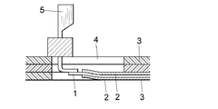
従来、ジョイントボックスには多数の型式が知られているが、例えばFFC(フレキシブルフラットケーブル)を積層して複雑な回路処理をしたものが本出願人による特許文献1で開示されている。このジョイントボックスでは、図28に示すように所定の回路パターンを形成した導体箔1を2枚の絶縁シート2により挟着したフラットケーブル層3を積層する。
Conventionally, many types of joint boxes are known. For example,
積層したフラットケーブル層3には共通の切欠孔4を形成し、各切欠孔4に必要に応じてフラットケーブル層3の導体箔1を露出し、露出した導体箔1を最上部に取り付けた接続端子5の下端部に溶着している。
A
しかしながら上述した従来例は、フラットケーブル層3の製作に手間がかかり、コストが高くなる。また、切欠孔4内での導体箔1の取り出しが厄介であり、また導体箔1と接続端子5との接続が不安定となる問題もある。
However, in the above-described conventional example, it takes time to manufacture the
本発明の目的は、上述の問題点を解消し、各種電気機器に使用することができ、金属箔による回路パターンを有する回路基板及びその製造方法及び回路基板を用いたジョイントボックスを提供することにある。 An object of the present invention is to provide a circuit board having a circuit pattern made of metal foil, a method for manufacturing the circuit board, and a joint box using the circuit board, which can be used for various electric devices, eliminating the above-described problems. is there.
上記目的を達成するための本発明に係る回路基板は、三次元的に成型した合成樹脂材から成る樹脂プレート上に、金属箔から成る回路パターンを載置したことを特徴とする。 In order to achieve the above object, a circuit board according to the present invention is characterized in that a circuit pattern made of a metal foil is placed on a resin plate made of a synthetic resin material three-dimensionally molded.
また、本発明に係る回路基板は、三次元的に成型した合成樹脂材から成る樹脂プレート上の必要個所に端子挿通孔を形成し、前記樹脂プレート上に所定形状に打ち抜いた金属箔から成る回路パターンを載置し、前記端子挿通孔に金属製の略円筒状の受端子を取り付け、該受端子に前記回路パターンを接続したことを特徴とする。 Further, the circuit board according to the present invention is a circuit made of a metal foil in which terminal insertion holes are formed at necessary positions on a resin plate made of a synthetic resin material molded three-dimensionally and punched into a predetermined shape on the resin plate. A pattern is placed, a metal substantially cylindrical receiving terminal is attached to the terminal insertion hole, and the circuit pattern is connected to the receiving terminal.
更に、本発明に係る回路基板は、三次元的に成型した合成樹脂材から成る樹脂プレート上の必要個所に端子挿通孔を形成し、前記樹脂プレート上に所定形状に打ち抜いた金属箔から成る回路パターンを載置し、前記端子挿通孔に該当する前記金属箔部分に接続端子の挿入端を挿し込むための切込部を設けると共に、対応する前記端子挿通孔に金属製の筒状の受端子を嵌合したことを特徴とする。 Further, the circuit board according to the present invention is a circuit made of a metal foil in which terminal insertion holes are formed at necessary portions on a resin plate made of a synthetic resin material three-dimensionally molded and punched into a predetermined shape on the resin plate. A pattern is provided, and a metal cylindrical receiving terminal is provided in the corresponding terminal insertion hole while providing a notch for inserting the insertion end of the connection terminal into the metal foil portion corresponding to the terminal insertion hole. It is characterized by fitting.
本発明に係る回路基板の製造方法は、三次元的に成型した合成樹脂材から成る樹脂プレート上に、所定形状に打ち抜いた金属箔から成る回路パターンを載置した回路基板において、前記金属箔からビク刃により前記回路パターンを打ち抜くと共に、前記回路パターンを前記ビク刃間に保持して前記樹脂プレート上に運搬し、前記樹脂プレート上に固定することを特徴とする。 A circuit board manufacturing method according to the present invention includes a circuit board in which a circuit pattern made of a metal foil punched into a predetermined shape is placed on a resin plate made of a synthetic resin material molded three-dimensionally. The circuit pattern is punched out by a big blade, the circuit pattern is held between the big blades, conveyed onto the resin plate, and fixed on the resin plate.
本発明に係る回路基板を用いたジョイントボックスは、三次元的に成型した合成樹脂材から成る樹脂プレート上に金属箔から成る回路パターンを載置した複数枚の回路基板を積層し、これらの回路基板の所定個所に前記積層した回路基板に共通の端子挿通孔を形成し、前記任意の層の回路基板の前記端子挿通孔に金属製の略円筒状の受端子を取り付け、該受端子に付設したタブを当該回路基板の前記回路パターンに接続し、前記共通の端子挿通孔にピン状の挿入端を有する挿入端子を挿通し、前記受端子を介して該当の前記回路基板の各層の前記回路パターンを電気的に導通することを特徴とする。 The joint box using the circuit board according to the present invention is obtained by laminating a plurality of circuit boards on which a circuit pattern made of a metal foil is placed on a resin plate made of a synthetic resin material three-dimensionally molded. A common terminal insertion hole is formed in the laminated circuit board at a predetermined position of the board, and a substantially cylindrical metal receiving terminal is attached to the terminal insertion hole of the circuit board of the arbitrary layer, and is attached to the receiving terminal. The tabs are connected to the circuit pattern of the circuit board, the insertion terminals having pin-like insertion ends are inserted into the common terminal insertion holes, and the circuits of the respective layers of the circuit board are inserted through the receiving terminals. The pattern is electrically conductive.
また、本発明に係る回路基板を用いたジョイントボックスは、三次元的に成型した合成樹脂材から成る樹脂プレート上の必要個所に端子挿通孔を形成し、前記樹脂プレート上に所定形状に打ち抜いた金属箔から成る回路パターンを載置し、前記端子挿通孔に該当する前記回路パターンにピン状の挿入端を挿し込むための切込部を設けると共に、対応する前記端子挿通孔に金属製の略円筒状の受端子を嵌合した複数枚の回路基板を積層し、前記端子挿通孔に前記挿入端を挿通し、前記受端子を介して前記挿入端と前記回路基板の各層の前記回路パターンとを電気的に導通することを特徴とする。 In addition, the joint box using the circuit board according to the present invention has a terminal insertion hole formed in a required portion on a resin plate made of a synthetic resin material molded three-dimensionally and punched into a predetermined shape on the resin plate. A circuit pattern made of a metal foil is placed, and a cut portion for inserting a pin-shaped insertion end into the circuit pattern corresponding to the terminal insertion hole is provided, and the corresponding metal insertion is made in the corresponding terminal insertion hole. A plurality of circuit boards fitted with cylindrical receiving terminals are stacked, the insertion end is inserted through the terminal insertion hole, and the insertion end and the circuit pattern of each layer of the circuit board are inserted through the receiving terminals. Are electrically conductive.
本発明に係る回路基板及びその製造方法によれば、成型された樹脂プレート上にビク刃等により打ち抜いた金属箔から成る回路パターンを載置するので構成が簡素であり、製作が容易である。 According to the circuit board and the manufacturing method thereof according to the present invention, since the circuit pattern made of the metal foil punched out by the big blade or the like is placed on the molded resin plate, the configuration is simple and the manufacture is easy.
本発明に係る回路基板を用いたジョイントボックスによれば、箔回路による回路パターンが形成された回路基板を積層して製作するので、複雑な回路でも薄型化して製作できる。 According to the joint box using the circuit board according to the present invention, the circuit board on which the circuit pattern by the foil circuit is formed is laminated and manufactured, so that even a complicated circuit can be manufactured with a reduced thickness.
12、97 回路ユニット
15 挿入端子
16 ブロック体
19、91 回路基板
20、92 樹脂プレート
20c、92b 端子挿通孔
21、93 箔回路
22 受端子
23 角型電線
41 銅箔
49、55 打ち抜きプレス
49a、55a ビク刃
55b 吸着パット
71 角型電線材
95 受リング
96 接続端子12, 97
本発明を図1〜図27に図示の実施例に基づいて詳細に説明する。 The present invention will be described in detail based on the embodiment shown in FIGS.
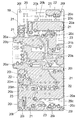
図1は本発明に係る回路基板を用いたジョイントボックスの実施例の分解斜視図であり、上ケース11、回路ユニット12、下ケース13を相互に組み付けることにより、ボックス形状のジョイントボックスが得られる。つまり、上ケース11、下ケース13間に回路ユニット12が収納され、ケース11、13同士が接合されると、回路ユニット12を収容した状態で上ケース11、下ケース13に設けられたロック部14a、14bによりロックされる。
FIG. 1 is an exploded perspective view of an embodiment of a joint box using a circuit board according to the present invention, and a box-shaped joint box is obtained by assembling an
回路ユニット12の上面には、図示を省略した回路パターンが形成されていると共に、複数個の挿入端子15を取り付けた合成樹脂製のブロック体16が配置されている。ブロック体16は上ケース11に区画された枠部17に嵌合され、ブロック体16上に突出した挿入端子15の平刃端15a、受端15b、ピン端15cなどの接続部が枠部17内に位置している。そして、これらの接続部にヒューズ素子、スイッチ素子或いは他の接続端子を収容したコネクタが装着可能とされている。
A circuit pattern (not shown) is formed on the upper surface of the
また、下ケース13においても枠部18が形成され、図示は省略しているが、回路ユニット12の下面に取り付けられたブロック体16から挿入端子15の接続端が下向きに突出され、下ケース13の下面に同様の素子、コネクタなどが装着可能とされている。
The
また、このジョイントボックス内に電子回路ユニットを設けることもでき、更にはジョイントボックスから端子を突出して、電子回路ユニットを収容したボックス同士を隣接して、端子同士により接続することもできる。 In addition, an electronic circuit unit can be provided in the joint box, and terminals can be protruded from the joint box so that boxes containing the electronic circuit units are adjacent to each other and connected by the terminals.
回路ユニット12は例えば5枚の回路基板19が積層され、図2、図3に示すように、各回路基板19は例えば射出成型により成型された合成樹脂製の最大厚み1.5mm程度の樹脂プレート20上に、パターンの箔回路21が載置されている。箔回路21は例えば厚さ120μmの銅箔から成り、積層された回路基板19ごとに異なるパターンに区画されている。
For example, five
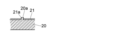
樹脂プレート20には、図4に示すように複数のアンカピン20aが上方に向けて突出され、箔回路21に設けられたピン孔21aに挿通されている。このアンカピン20aの上部を熱により押し潰すことにより、箔回路21は樹脂プレート20に位置決め固定されている。
As shown in FIG. 4, a plurality of anchor pins 20 a protrude upward in the
なお、電流容量によっては一部の箔回路21は、図5に示すように金属箔を2層又はそれ以上の複数層とされ、高さの高いアンカピン20a’により固定されている。樹脂プレート20に穿孔された溶着用孔部20bから溶着電極を挿し込むことにより、重ねた金属箔21同士は溶着される。
Depending on the current capacity, as shown in FIG. 5, some of the
樹脂プレート20の複数個所には、図2、図3に示すように積層した樹脂プレート20に共通の円形の端子挿通孔20cが形成され、所定の層の回路基板19の各回路21には端子挿通孔20cと同径の孔部が設けられていて、この端子挿通孔20cには受端子22が取り付けられている。なお、受端子22は必要な電流容量によって数種類の大きさがあり、それに伴って端子挿通孔20cの径も数種類設けられている。
As shown in FIGS. 2 and 3, circular
受端子22は例えば肉厚0.2mmの黄銅板から成り、フォーミングプレスにより形成されている。この受端子22は図6に示すように、短円筒状に形成した筒状接続部22aの上部にフランジ部22bが形成され、更にフランジ部22bの一部にタブ22cが付設されている。なお、筒状接続部22aとフランジ部22bとの境界部は、後述する挿入端子を受け入れるためのテーパ状の案内部22dとされている。
The receiving
図7は5枚の回路基板19を積層し、受端子22を固定した状態の回路ユニット12の要部断面図であり、回路基板19の端子挿通孔20cの中間部の内径を受端子22の筒状接続部22aの外径とほぼ同じとしている。端子挿通孔20cの上部の周囲は上方に持ち上げられた円環部20dとされ、この円環部20d内に受端子22のフランジ部22bを載置する段部20eが形成されている。端子挿通孔20cの下部は筒状接続部22aの下部を拡開するために内径が大きくされている。
FIG. 7 is a cross-sectional view of the main part of the
なお図示においては、受端子22を取り付けない端子挿通孔20cの内径は、受端子22の内径とほぼ同じ大きさとしているが、受端子22を取り付ける端子挿通孔20cと同形状にしても支障はない。
In the figure, the inner diameter of the
受端子22の筒状接続部22aは端子挿通孔20c内に配置され、筒状接続部22aの下部は端子挿通孔20cの下部にテーパ状にかしめ止めされている。この筒状接続部22aの下部の拡開は、受端子22の回路基板19への固定を主目的としているが、下面方向から挿入端子15を挿し込む場合におけるテーパ状の案内部22eともなっている。また、タブ22cは回路基板19の箔回路21上に溶着により接続されており、この溶着のためにタブ22cの下方の樹脂プレート20には、電極挿通のための溶着用孔部20fが形成されている。
The
回路基板19の受端子22を取り付けない端子挿通孔20cにおいては、その上部周囲に円環部20gが形成され、端子挿通孔20cの周囲に箔回路21が存在していても、挿入される挿入端子15が箔回路21と接触しないようにされている。なお、回路ユニット12の最上位の回路基板19に設けた円環部20gは、ブロック体16を安定して載置するために、受端子22を取り付ける端子挿通孔20cに設けた円環部20dと同じ高さとされている。
In the
また、図2、図3に示すように樹脂プレート20の下面側には必要に応じて電線用溝部20hが形成され、この電線用溝部20h内に絶縁塗料が塗布された例えば角型電線23が装着されている。角型電線23の両端部は電線用溝部20hの両端に設けられた電線用孔部20iを介して立ち上げられて箔回路21の下面と溶着し、回路設計上、樹脂プレート20の表面においては接続できない箔回路21のパターン同士をジャンパ線として短絡するようにされている。なお、この角型電線23は電流容量に応じて各種断面積のものが使用されている。
Also, as shown in FIGS. 2 and 3, a
上述の回路基板19のアンカピン20aの熱溶融した上端部、円環部20d、受端子22は、上層の樹脂プレート20の下面に形成した凹部内に嵌まり込み、積層した回路基板19同士が密着すると共に、水平方向にずれないようにされている。例えば、図3に示す凹部20jは、下層の回路基板19に取り付けた受端子22が嵌まり込む部分である。また、樹脂プレート20の四隅に設けた透孔20lは回路基板19を積層する場合の位置合わせ孔である。
The heat-melted upper end of the
また、回路基板19に設けられた図2、図3に示す角孔20mは、挿入端子15、受端子22では電流容量が足りない場合に、図1に示す大電流用の接続端子26を取り付けるためのものであり、回路ユニット12の最上位の回路基板19のみに設けられている。
2 and 3 provided in the
回路基板19は全ての箔回路21を上に向けて積層するとは限らず、図7においては上層の3層の回路基板19は箔回路21を上に向けて積層し、下層の2層の回路基板19は箔回路21を下に向けて積層されている。この場合においても、3層目と4層目の下面同士を重ねた回路基板19では、図示を省略しているが、ずれが生じないように部分的に嵌合し得るようにされている。
The
図8は受端子22に挿入するための挿入端子15の斜視図を示し、挿入端子15の下部は受端子22の筒状接続部22aに挿入するための断面略四角形のピン状挿入端15dとされている。中間部15eを介しての上部は上ケース11上に突出して、他の接続端子と接続するための平刃端15aとされている。なお、この平刃端15aは、図1に示す受端15b或いはピン端15cとすることもできる。
FIG. 8 is a perspective view of the
この挿入端15dによれば、板厚の薄い金属板を折り曲げ、空洞部がなく上下方向に幅のある断面略四角形の棒状に形成している。従って金属板の板厚が薄い場合でも、金属板の厚みと比較して一辺の厚みが十分に大きい挿入端15dを得ることができ、挿入端15dが弯曲したり或いは折損することが少ない。また、上部の平刃端15aも金属板を二重に折り畳んで厚みを持たせている。
According to the
更に、挿入端受端子22への挿入時にクリック感を得るためと、接続を良好とするために、挿入端15dに複数の段部を形成してもよい。また、これらの挿入端15dは受端子22の大きさに合わせて数種類用意されている。
Further, a plurality of step portions may be formed on the
合成樹脂材によるブロック体16に設けられた挿通孔には、幾つかの挿入端子15の中間部15eが挿し込まれて固定され、図1に示すように、挿入端15dはまとめて回路基板19に挿入されている。なお、挿入端子15の中間部15eには、挿通孔に固定するための図示しない爪部が設けられている。
図9に示すように、ブロック体16の底部には単数又は複数の下方を向くアンカピン16aが一体に形成されており、箔回路21に設けられたピン孔21b、各樹脂プレート20に共通に設けられたピン孔20kに挿通されている。最下層の回路基板19から下方に突出したアンカピン16aの下端を溶融して押し潰すことにより、ブロック体16を回路ユニット12に固定すると共に、回路基板19の積層体同士を分離不能に固定している。
As shown in FIG. 9, one or a plurality of downwardly facing anchor pins 16 a are integrally formed on the bottom of the
図10は回路基板19の他の例を示し、回路基板19の積層体においては、下方の回路基板19ほど端子挿通孔20cの径は小さくされており、これに伴って受端子22の径も小径とされている。同時に、この積層体に挿入される挿入端子15においても、図11に示すようにピン状挿入端15dは、受端子22の径に合わせて先端ほど小径とされている。このような構成により、ブロック体16に固定された挿入端子15を回路基板19の積層体に挿入する際に、挿入が容易となる利点がある。
FIG. 10 shows another example of the
図12は上述の回路基板19の製造工程の説明図である。箔回路21の母材である銅箔41はローラ42にコイル状に巻回されており、必要に応じて銅箔41に予め形成したパイロット孔を基に、銅箔にはクランプなどの送り手段43により間欠的に繰り出される。銅箔41は孔あけプレス工程に搬送され、孔あけプレス44により複数の所定位置にピン孔21a、21bが穿孔され、樹脂プレート20との積層工程に移送される。なお、銅箔41に設けるピン孔21aは箔回路21を樹脂プレート20に固定するものであるので、樹脂プレート20上に残り、箔回路21となるべき部分に設けられる。
FIG. 12 is an explanatory diagram of the manufacturing process of the
一方、樹脂プレート20はストッカ45に積層されており、銅箔41の搬送に同期して1枚ずつ取り出される。樹脂プレート20は合成樹脂膜を射出成形或いは合成樹脂基材をホットプレスすることにより製造され、アンカピン20a、孔部20b、20f、端子挿通孔20c、円環部20d、20g、段部20e、電線用溝部20h、孔部20i、凹部20j、ピン孔20k、透孔20l等が既に形成されている。
On the other hand, the
1枚の樹脂プレート20が積層台46上に載置されると、積層台46は上昇して銅箔41に向けて押し上げられる。樹脂プレート20のアンカピン20aが銅箔41に穿孔されたピン孔21aに入り込むように、撮像カメラ47による画像処理によって積層台46は三次元的に位置制御される。
When one
なお、特に電流容量を要する箔回路21には、前述したように銅箔41を二重に重ねて電気抵抗を少なくするので、上述の工程を2回繰り返し、図示しない工程により、重ねられた銅箔41同士を図5に示したように樹脂プレート20に設けた溶着用孔部20bを用いて溶着する。
In particular, in the
アンカピン20aをピン孔21aに挿入して銅箔41を樹脂プレート20上に重ねた後に、積層台46の上方に位置する熱プレス48を降下し、アンカピン20aの頂部を熱により押し潰し、銅箔41が樹脂プレート20から剥離しないようにする。なお、位置合わせに伴って、ブロック体16のアンカピン16aを挿通する銅箔41のピン孔21bは、樹脂プレート20のピン孔20kと一致している。
After the
続いて、樹脂プレート20と一体となった銅箔41を打ち抜きプレス49に搬送し、画像処理を行いながら銅箔41から箔回路21を打ち抜く。上側の打ち抜きプレス49はビク刃49aを有し、樹脂プレート20を傷付けることなく銅箔41から箔回路21を打ち抜くものであり、ビク刃49aによって箔回路21の回路パターンが打ち抜かれることになる。また、この回路パターンの打ち抜きに際して、回路パターン中の端子挿通孔20c上に位置する銅箔41はその回路基板19において受端子22に接続する場合には受端子22の内径通りの孔部が形成され、受端子22と接続しない場合には円環部20gの外側の大きさの孔部が形成される。
Subsequently, the
更に、樹脂プレート20と共に銅箔41を搬送し、箔回路21で使用されない残材の銅箔41は、樹脂プレート20から剥離された後に残材処理刃50により細断され、残材ボックス51内に投棄される。一方、箔回路21を表面に一体に固定した樹脂プレート20は、回路基板19として所定方向に搬出され、ストッカ52内に積層される。
Further, the
図13は他の方法による回路基板19の製造工程の説明図であり、図12と同一の符号は同一の部材を示している。箔回路21の母材である銅箔41はローラ42にコイル状に巻回されており、銅箔41に孔あけプレス44により複数の所定位置にピン孔21a、21bが穿孔され、パターン回路打ち抜き工程に移送されることは図12の場合と同様である。
FIG. 13 is an explanatory view of the manufacturing process of the
続いて、銅箔41を打ち抜きプレス55に搬送し、画像処理を行いながら銅箔41から箔回路21を打ち抜く。図14に示すように上側の打ち抜きプレス55はビク刃55aを有し、銅箔41から箔回路21を打ち抜き、ビク刃55aによって箔回路21の回路パターンが打ち抜かれることになる。ビク刃55a間には、複数の吸着パット55bが設けられ、打ち抜いた箔回路21を真空吸引して保持し、ビク刃運搬装置により所定位置に運搬する。
Subsequently, the
箔回路21として打ち抜かれない残材の銅箔41は、更に運搬され残材処理刃56により細断され、残材ボックス57内に投棄される。
The remaining
一方、樹脂プレート20はストッカ45に積層されており、銅箔41からの箔回路21の打ち抜きと同期して、1枚の樹脂プレート20が積層台46上に載置されると、ビク刃55aに保持された箔回路21が樹脂プレート20上に運ばれる。そして、撮像カメラ58による画像処理による三次元的な位置制御により樹脂プレート20のアンカピン20aが箔回路21に穿孔されたピン孔21aに入り込むようにビク刃運搬装置が制御される。
On the other hand, the
アンカピン20aを箔回路21のピン孔21aに挿入して、箔回路21を樹脂プレート20上に重ねた後に、ビク刃55a間の吸着パット55bから空気を噴出して箔回路21をビク刃55aから分離し樹脂プレート20上に押し付ける。この箔回路21の押し付けは、ビク刃55a間に複数の押し出しピンを設け、箔回路21を樹脂プレート20上に押し付けてもよい。
After the
その後に、ビク刃55aをビク刃運搬装置により、元の打ち抜きプレス55の位置に戻し、箔回路21を載置した樹脂プレート20上に、上方に位置する熱プレス48を降下し、アンカピン20aの頂部を押し潰し、箔回路21を樹脂プレート20上に固定する。
Thereafter, the
図15〜図17は回路基板19に受端子22を固定する工程の説明図であり、パーツフィーダにより整列して供給される受端子22を図15に示すように、ロボットハンド61により必要に応じて撮像カメラ62により画像処理を行いながら保持して、回路基板19の必要個所に運搬する。ロボットハンド61には筒部63に対して吊り上げピン64が上下動自在に設けられている。この吊り上げピン64を受端子22の筒状接続部22aに挿入し、摩擦抵抗により受端子22を持ち上げ、受端子22のタブ22cが箔回路21上に載置されるように、画像処理により位置調整しながら受端子22を樹脂プレート20の端子挿通孔20cに挿入する。
15 to 17 are explanatory views of a process of fixing the receiving
筒部63により受端子22を樹脂プレート20の段部20e上に押し付けたまま、吊り上げピン64を図16に示すように上方に持ち上げる。続いて、下方から先端を円錐状としたプレスピン65を持ち上げて、筒状接続部22aの下部を押し広げ、受端子22を端子挿通孔20cの下部にかしめ止めする。
While the receiving
その後に、図17に示すようにタブ22cを箔回路21に電極66、67を用いて溶着する。電極66、67の先端はそれぞれ直径1mm前後の細径丸型とされ、上方の電極66はタブ22cに接触し、下方の電極67は箔回路21の下面に溶着用孔部20fを介して接触する。なお、この溶着はロボットハンドにより順次に行うこともできるが、多数本の電極を用いて一括して溶着することもできる。
Thereafter, as shown in FIG. 17, the
図18〜図20は角型電線23を樹脂プレート20の電線用溝部20hに固定する工程の説明図であり、図18において例えば0.3×3mmの偏平な角銅線に絶縁層が塗布された角型電線材71はローラ72に巻回され、間欠的に繰り出されて供給される。ローラ72から供給された角型電線材71は矯正ロール73により捩りなどが矯正され、計尺ローラ74により繰り出し長さが計測され、所定長が繰り出されたところでチャック75により固定される。この状態において、被覆剥ぎ機76によって角型電線材71の端部の絶縁層を剥離し、次いで剥離部分が切断機77に進んだところでチャック78により固定し、切断機77により剥離部分の中央を切断する。
18 to 20 are explanatory views of a process of fixing the rectangular
このようにして、両端の絶縁層が剥離された所定長の角型電線23が得られる。この角型電線23を図19に示すように加工プレス機79により両端を折り曲げ、ロボットハンドにより樹脂プレート20を裏返して裏側の電線用溝部20h内に角型電線23を装着し、図20に示すように撮像カメラ80により画像処理を行いながら、両端の絶縁剥離部を樹脂プレート20の溶着用孔部20iを介して箔回路21の下面に押し当て、上下の電極81、82を用いて角型電線23を箔回路21に溶着して電気的に接続する。
In this way, a rectangular
このようにして製作され、それぞれ回路パターンが異なる複数枚の回路基板19を積層し、先の図9に示すようにブロック体16を回路基板19の積層体上に載置し、ブロック体16に固定された挿入端子15の挿入端15dを、回路基板19の端子挿通孔20cに挿入すると、挿入端15dは少なくとも何れかの回路基板19に取り付けられた受端子22の筒状接続部22aに挿入される。
A plurality of
このとき、挿入端15dは断面略四角状とされているので、受端子22の筒状接続部22aに挿入された場合に角部が良好に接触し、挿入端子15は何れかの回路基板19の箔回路21と良好な電気的な接続がなされることになる。また必要に応じて、回路ユニット12の下面側からもブロック体16を装着する。
At this time, since the
挿入端15dの挿入と同時に、ブロック体16から突出されたアンカピン16aは回路基板19の積層体のピン孔20kを貫通するので、ピン孔20kから突出した先端を溶融すると回路ユニット12が完成する。
Simultaneously with the insertion of the
この回路ユニット12を上ケース11、下ケース13により挟み込み、ロック部14a、14bによりケース11、13同士をロックする。上ケース11、下ケース13の表面から突出する挿入端子15の平刃端15a、受端15b、ピン端15cに、上述したように各種素子、コネクタを取り付けることによりジョイントボックスとして機能する。
The
図21以降は他の回路基板91の実施例を示している。図21に示すように、各回路基板91は射出成型により成型された合成樹脂製の例えば最大厚み1.5mm程度の樹脂プレート92上に、例えば厚さ120μmの銅等の金属箔から成り、積層された回路基板91ごとに異なる区画がなされたパターンの箔回路93が載置されている。なお、樹脂プレート92には必要に応じて、箔回路93を載置し位置決めするために、箔回路93の厚みと同等の深さを有する凹部94が箔回路93と同形状に形成されている。
FIG. 21 and subsequent figures show
樹脂プレート92には、複数のアンカピン92aが上方に向けて突出され、箔回路93に設けられたピン孔93aに挿通され、アンカピン92aの上部を熱により押し潰すことにより、箔回路93は樹脂プレート92上に位置決め固定されている。なお、電流容量を必要とする場合には、実施例1と同様に一部の箔回路93は銅箔を2層又はそれ以上の複数層としてもよい。
A plurality of anchor pins 92a protrude upward from the
樹脂プレート92の複数個所には、積層した樹脂プレート92に共通の円形の端子挿通孔92bが形成され、所定の層の回路基板91の所定の端子挿通孔92bには、図22に拡大して示す円筒状や角筒状の受リング95が嵌合されている。なお、受リング95は後述する挿入端子の種類や電流容量によって数種類の大きさが用いられ、それに伴って端子挿通孔92bの径も数種類設けられており、例えばステンレス製の丸パイプや角パイプを切断して造られている。なお、図23に示すように、受リング95にフランジ部95aを設けてもよい。
Circular terminal insertion holes 92b common to the
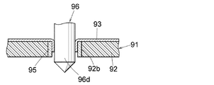
端子挿通孔92bに嵌合された受リング95上の箔回路93には、十字状の切込部93bが設けられており、図24に示すように例えば接続端子96の棒状の挿入端96dを挿入することにより、箔回路93の切込部93bが破られ、押し拡げられて、箔回路93は挿入端96dと受リング95の間に挟み込まれ、挿入端96dと箔回路93は導電的に接触する。なお、導通を必要としない挿入端には受リング95は嵌合されておらず、また挿通孔92bの周囲の回路パターンは導通が生じないように孔部が設けられたり除去されている。
The
この場合に、挿入端96dの先端を図21に示すように尖らせることにより、挿込が容易となる。また、挿入端96dを同様に図21に示すように断面角形とすることにより、切込部93bを破り易くなり、受リング95に対する接触がより確実となる。
In this case, insertion is facilitated by sharpening the tip of the
なお、挿入端96dを挿入するには、図25(a)に示す十字状の切込部93bだけではなく、(b)に示すように丸孔93c、(c)に示すように角孔93dの切込部とすることもできる。
In order to insert the
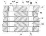
図26は5枚の回路基板91を積層した状態の回路ユニット97の要部断面図である。また回路基板91の四隅には、回路基板91を積層する場合の図示しない凹凸部が形成され、これらの凹凸部同士を嵌合することにより上下の回路基板91が位置決めされる。
FIG. 26 is a cross-sectional view of the main part of the
このようにして、それぞれ回路パターンが異なる複数枚の回路基板91を積層し、図27に示すようにブロック体16を最上層の回路基板91上に載置し、ブロック体16に固定された接続端子96の挿入端96dを、回路基板91の端子挿通孔92bに挿入すると、挿入端96dは少なくとも何れかの回路基板91に取り付けられた受リング95内に挿入される。挿入端96dは受リング95ごとに設けられた箔回路93と導通し、積層した回路基板91を用いた立体的な回路ユニット97が構成されることになる。
In this way, a plurality of
Claims (22)
Applications Claiming Priority (7)
| Application Number | Priority Date | Filing Date | Title |
|---|---|---|---|
| JP2004105997 | 2004-03-31 | ||
| JP2004105997 | 2004-03-31 | ||
| JP2004239707 | 2004-08-19 | ||
| JP2004239707 | 2004-08-19 | ||
| JP2004381266 | 2004-12-28 | ||
| JP2004381266 | 2004-12-28 | ||
| PCT/JP2005/005811 WO2005096683A1 (en) | 2004-03-31 | 2005-03-29 | Circuit board, its manufacturing method, and joint box using circuit board |
Related Child Applications (2)
| Application Number | Title | Priority Date | Filing Date |
|---|---|---|---|
| JP2008073717A Division JP4719759B2 (en) | 2004-03-31 | 2008-03-21 | Circuit board manufacturing method |
| JP2008073718A Division JP4823262B2 (en) | 2004-03-31 | 2008-03-21 | Joint box using circuit board |
Publications (1)
| Publication Number | Publication Date |
|---|---|
| JPWO2005096683A1 true JPWO2005096683A1 (en) | 2008-02-21 |
Family
ID=35064168
Family Applications (4)
| Application Number | Title | Priority Date | Filing Date |
|---|---|---|---|
| JP2006511657A Pending JPWO2005096683A1 (en) | 2004-03-31 | 2005-03-29 | Circuit board, manufacturing method thereof, and joint box using circuit board |
| JP2008073717A Expired - Fee Related JP4719759B2 (en) | 2004-03-31 | 2008-03-21 | Circuit board manufacturing method |
| JP2008073718A Expired - Fee Related JP4823262B2 (en) | 2004-03-31 | 2008-03-21 | Joint box using circuit board |
| JP2009097640A Expired - Fee Related JP4938046B2 (en) | 2004-03-31 | 2009-04-14 | Joint box using circuit board |
Family Applications After (3)
| Application Number | Title | Priority Date | Filing Date |
|---|---|---|---|
| JP2008073717A Expired - Fee Related JP4719759B2 (en) | 2004-03-31 | 2008-03-21 | Circuit board manufacturing method |
| JP2008073718A Expired - Fee Related JP4823262B2 (en) | 2004-03-31 | 2008-03-21 | Joint box using circuit board |
| JP2009097640A Expired - Fee Related JP4938046B2 (en) | 2004-03-31 | 2009-04-14 | Joint box using circuit board |
Country Status (6)
| Country | Link |
|---|---|
| US (3) | US7943859B2 (en) |
| EP (1) | EP1737282A4 (en) |
| JP (4) | JPWO2005096683A1 (en) |
| KR (3) | KR101208823B1 (en) |
| CN (2) | CN101568227B (en) |
| WO (1) | WO2005096683A1 (en) |
Families Citing this family (31)
| Publication number | Priority date | Publication date | Assignee | Title |
|---|---|---|---|---|
| CN101568227B (en) * | 2004-03-31 | 2011-09-28 | 三菱电线工业株式会社 | Circuit board, manufacturing method thereof, and joint box using circuit board |
| DE102007028511A1 (en) * | 2007-06-21 | 2008-12-24 | Robert Bosch Gmbh | Electronic device with at least one electrical connection element and method for producing a connection element |
| DE102008008278A1 (en) * | 2008-02-07 | 2009-08-13 | Dr. Johannes Heidenhain Gmbh | Angle measuring device |
| JP2010027957A (en) * | 2008-07-23 | 2010-02-04 | Mitsubishi Cable Ind Ltd | Circuit structure, joint box, and method of manufacturing circuit structure |
| JP5255365B2 (en) * | 2008-08-09 | 2013-08-07 | 古河電気工業株式会社 | Relay terminal member, circuit structure including the same, and electronic unit |
| JP5497389B2 (en) * | 2009-09-17 | 2014-05-21 | 三菱マテリアル株式会社 | Electrical junction box |
| JP5758584B2 (en) | 2010-03-18 | 2015-08-05 | 本田技研工業株式会社 | Junction box |
| CN101958521A (en) * | 2010-09-19 | 2011-01-26 | 淮南润成科技有限公司 | Distributing box for mine substantial security circuit |
| JP5610285B2 (en) * | 2010-09-29 | 2014-10-22 | 本田技研工業株式会社 | Wiring structure and joint box including the same |
| DE102011102484B4 (en) | 2011-05-24 | 2020-03-05 | Jumatech Gmbh | Printed circuit board with molded part and process for its production |
| US8491315B1 (en) * | 2011-11-29 | 2013-07-23 | Plastronics Socket Partners, Ltd. | Micro via adapter socket |
| US9536798B2 (en) * | 2012-02-22 | 2017-01-03 | Cyntec Co., Ltd. | Package structure and the method to fabricate thereof |
| JP5952039B2 (en) * | 2012-03-15 | 2016-07-13 | 住友精密工業株式会社 | Discharge cell and ozone gas generator |
| DE102012009651A1 (en) * | 2012-05-14 | 2013-11-14 | Robert Bosch Gmbh | Connection unit for drive device, has terminal pins that are provided at injection molding structure for electrically connecting electrical terminal of electrical loads to an electrical energy source |
| DE202012010075U1 (en) * | 2012-10-22 | 2012-11-13 | Truma Gerätetechnik GmbH & Co. KG | Central unit for shunting drive |
| JP2015049053A (en) * | 2013-08-29 | 2015-03-16 | アルプス・グリーンデバイス株式会社 | Current detector |
| CN104953011B (en) * | 2015-06-26 | 2016-05-11 | 深圳市峻泽科技有限公司 | A kind of substrate and manufacture method thereof with metal level |
| US9994407B2 (en) | 2015-11-06 | 2018-06-12 | Nxp B.V. | System and method for processing a flexible substrate |
| US10104784B2 (en) | 2015-11-06 | 2018-10-16 | Nxp B.V. | Method for making an electronic product with flexible substrate |
| US20170223816A1 (en) * | 2016-02-01 | 2017-08-03 | Ibiden Co., Ltd. | Flexible printed wiring board, electronic device having flexible printed wiring board, and method for manufacturing electronic device having flexible printed wiring board |
| CN110062985B (en) * | 2016-12-19 | 2021-07-09 | Abb瑞士股份有限公司 | Multi-phase busbar for conducting electrical energy and method for producing same |
| JP2019029535A (en) * | 2017-07-31 | 2019-02-21 | イビデン株式会社 | Flexible printed wiring board, electronic device having flexible printed wiring board, method for manufacturing electronic device having flexible printed wiring board |
| GB2566943B (en) * | 2017-09-25 | 2020-09-02 | Ge Aviat Systems Ltd | Surface mount connector and method of forming a printed circuit board |
| JP6666320B2 (en) | 2017-11-21 | 2020-03-13 | ファナック株式会社 | Mounting structure of resin molded board and capacitor |
| JP7094619B2 (en) | 2018-01-29 | 2022-07-04 | 矢崎総業株式会社 | Route structure and method |
| CN108901134B (en) * | 2018-07-12 | 2023-07-25 | 深圳智慧者机器人科技有限公司 | Copper plate assembling device |
| JP7289706B2 (en) * | 2019-04-08 | 2023-06-12 | 矢崎エナジーシステム株式会社 | joint box |
| US11374366B2 (en) | 2020-06-19 | 2022-06-28 | Lear Corporation | System and method for providing an electrical ground connection for a circuit assembly |
| US11646514B2 (en) | 2020-08-10 | 2023-05-09 | Lear Corporation | Surface mount technology terminal header and method for providing an electrical connection to a printed circuit board |
| US11706867B2 (en) | 2021-01-27 | 2023-07-18 | Lear Corporation | System and method for providing an electrical ground connection for a circuit assembly |
| CN113161948B (en) * | 2021-02-09 | 2022-12-09 | 国网福建省电力有限公司明溪县供电公司 | Extrusion type self-sealing type junction box |
Citations (6)
| Publication number | Priority date | Publication date | Assignee | Title |
|---|---|---|---|---|
| JPH04345082A (en) * | 1991-05-22 | 1992-12-01 | Mitsubishi Electric Corp | Large current wiring board |
| JPH05167207A (en) * | 1991-12-13 | 1993-07-02 | Okuma Mach Works Ltd | Printed board for power circuit wiring and manufacture thereof |
| JPH07122825A (en) * | 1993-10-22 | 1995-05-12 | Sharp Corp | Solid molded circuit substrate and its manufacture |
| JPH08223742A (en) * | 1995-02-14 | 1996-08-30 | Sumitomo Wiring Syst Ltd | Branch connection box |
| JPH09163516A (en) * | 1995-12-06 | 1997-06-20 | Yazaki Corp | Interconnection board and its manufacture |
| JP2001264276A (en) * | 2000-03-21 | 2001-09-26 | Polyplastics Co | Sensor with circuit formed by metal foil transfer |
Family Cites Families (62)
| Publication number | Priority date | Publication date | Assignee | Title |
|---|---|---|---|---|
| US3674914A (en) * | 1968-02-09 | 1972-07-04 | Photocircuits Corp | Wire scribed circuit boards and method of manufacture |
| US3688248A (en) * | 1968-08-13 | 1972-08-29 | Henry John Modrey | Roller metal pin for use as electric connector or fastener |
| FR2217906B3 (en) * | 1973-02-15 | 1976-02-13 | Radiall Fr | |
| JPS5575294A (en) * | 1978-12-02 | 1980-06-06 | Sumitomo Electric Industries | Method of connecting back and front surfaces of bothhside printed circuit board |
| US4333233A (en) * | 1979-02-19 | 1982-06-08 | Guardall Limited | Machines and method applicable to the manufacture of electrical and like devices |
| US4435741A (en) * | 1980-09-03 | 1984-03-06 | Canon Kabushiki Kaisha | Electrical circuit elements combination |
| JPS58106971U (en) * | 1982-01-14 | 1983-07-21 | 棚沢 日佐司 | printed wiring board |
| US4487463A (en) * | 1983-02-22 | 1984-12-11 | Gulf & Western Manufacturing Company | Multiple contact header assembly |
| JPS59230741A (en) * | 1983-06-15 | 1984-12-25 | 株式会社日立製作所 | Shape memory composite material |
| JPS618960U (en) * | 1984-06-22 | 1986-01-20 | 日本航空電子工業株式会社 | Elastic pin for press-fitting |
| US4641426A (en) * | 1985-06-21 | 1987-02-10 | Associated Enterprises, Inc. | Surface mount compatible connector system with mechanical integrity |
| ATE61162T1 (en) * | 1985-12-11 | 1991-03-15 | Burndy Electra Nv | CONTACT PIN. |
| JPS63127222U (en) * | 1987-02-09 | 1988-08-19 | ||
| JPS63229897A (en) * | 1987-03-19 | 1988-09-26 | 古河電気工業株式会社 | Manufacture of rigid type multilayer printed circuit board |
| US4937932A (en) * | 1987-04-10 | 1990-07-03 | Ishii Hyoki Co., Ltd. | Membrane panel switch |
| US4769907A (en) * | 1987-07-27 | 1988-09-13 | Northern Telecom Limited | Method of making a circuit board pin |
| US4948375A (en) * | 1987-08-25 | 1990-08-14 | Howard Lawrence | Adaptor assembly for circuit boards |
| US4867691A (en) * | 1987-10-29 | 1989-09-19 | E. I. Du Pont De Nemours And Company | Connector having expansible barrel with a layer of reflowable solder material thereon |
| JP2582142B2 (en) * | 1988-04-27 | 1997-02-19 | 日本電信電話株式会社 | Matrix switch board, matrix switch board connection pin, and method of manufacturing matrix board |
| US4950170A (en) * | 1988-06-23 | 1990-08-21 | Ltv Aerospace & Defense Company | Minimal space printed circuit board and electrical connector system |
| US4996629A (en) * | 1988-11-14 | 1991-02-26 | International Business Machines Corporation | Circuit board with self-supporting connection between sides |
| JPH02239684A (en) * | 1989-03-14 | 1990-09-21 | Yazaki Corp | Formation of circuit pattern on resin compact |
| JPH0744041Y2 (en) * | 1990-04-30 | 1995-10-09 | 古河電気工業株式会社 | Printed wiring board for large current |
| JP2827621B2 (en) * | 1991-10-23 | 1998-11-25 | 三菱電機株式会社 | High current substrate and method of manufacturing the same |
| US5373626A (en) * | 1993-01-06 | 1994-12-20 | Elco Corporation | Removable pin carrier |
| JP2849888B2 (en) * | 1993-02-02 | 1999-01-27 | 矢崎総業株式会社 | Wiring junction box |
| JP3163592B2 (en) * | 1993-04-01 | 2001-05-08 | 矢崎総業株式会社 | Composite circuit board |
| US5456608A (en) * | 1993-08-25 | 1995-10-10 | Conx Corporation | Cross-connect system |
| US6031349A (en) * | 1993-08-25 | 2000-02-29 | Con-X Corporation | Cross-connect method and apparatus |
| JP3170124B2 (en) * | 1993-12-07 | 2001-05-28 | 矢崎総業株式会社 | Circuit body multi-layer connection structure and circuit body multi-layer connection method |
| JPH09506328A (en) * | 1993-12-08 | 1997-06-24 | マサチューセッツ・インスティテュート・オブ・テクノロジー | Casting tool |
| US5836582A (en) * | 1994-04-04 | 1998-11-17 | Canon Kabushiki Kaisha | Sheet feeding device with air injectors for separating sheets |
| EP0708046A1 (en) * | 1994-10-21 | 1996-04-24 | Maschinenfabrik Gietz Ag | Register and feeding device |
| JPH08153425A (en) * | 1994-11-28 | 1996-06-11 | Furukawa Electric Co Ltd:The | Manufacture of flat circuit body |
| US5788513A (en) * | 1995-01-11 | 1998-08-04 | Enplas Corporation | IC socket |
| JPH08222825A (en) * | 1995-02-13 | 1996-08-30 | Nec Corp | Connecting structure of printed board |
| JPH08322127A (en) * | 1995-05-23 | 1996-12-03 | Sumitomo Wiring Syst Ltd | Laminated structure of bus bar and insulating plate contained in electric connection case |
| JPH09153516A (en) | 1995-11-30 | 1997-06-10 | Sumitomo Bakelite Co Ltd | Semiconductor device and ic chip inspecting method |
| US5914534A (en) * | 1996-05-03 | 1999-06-22 | Ford Motor Company | Three-dimensional multi-layer molded electronic device and method for manufacturing same |
| JPH10243526A (en) | 1997-02-21 | 1998-09-11 | Ryosei Denso Kk | Joint box |
| DE19707709C1 (en) | 1997-02-26 | 1998-04-16 | Siemens Ag | Relay modules circuit board e.g. for automobile |
| DE19709551A1 (en) * | 1997-03-07 | 1998-09-10 | Wuerth Elektronik Gmbh & Co Kg | Electrical printed circuit board |
| JP3201516B2 (en) * | 1997-07-18 | 2001-08-20 | ユーエイチティー株式会社 | Perforator |
| JP2001127242A (en) * | 1999-10-22 | 2001-05-11 | Seiko Epson Corp | Semiconductor chip, multichip package, semiconductor device, and electronic equipment, and manufacturing method thereof |
| US6483041B1 (en) * | 1999-11-12 | 2002-11-19 | Emc Corporation | Micro soldered connection |
| JP2001145241A (en) | 1999-11-15 | 2001-05-25 | Sumitomo Wiring Syst Ltd | Wiring board assembly |
| FR2806249B1 (en) * | 2000-03-13 | 2002-05-10 | Axo Scintex Cie Equip Automobi | MOUNTING OF CUT-OUT CIRCUITS ON LAMP SUPPORTS |
| JP2001307795A (en) * | 2000-04-18 | 2001-11-02 | Yazaki Corp | Wiring unit and electric connection box |
| JP2001343906A (en) * | 2000-05-31 | 2001-12-14 | Internatl Business Mach Corp <Ibm> | Display device, liquid crystal display device, method of production and connection for liquid crystal display device |
| JP2001359222A (en) * | 2000-06-13 | 2001-12-26 | Yazaki Corp | Electrical connection box |
| JP2002034126A (en) | 2000-07-19 | 2002-01-31 | Yazaki Corp | Wiring unit |
| JP2002374049A (en) * | 2001-06-13 | 2002-12-26 | Densei Lambda Kk | Mounting structure for power-supply device |
| JP2003017163A (en) * | 2001-06-27 | 2003-01-17 | Gunma Denki Kk | Multi-pin connector for mounting on sub-board and mounting method of parts on printed circuit board |
| JP3884931B2 (en) * | 2001-08-31 | 2007-02-21 | アルプス電気株式会社 | Electronic device FPC connection structure |
| JP2003142178A (en) * | 2001-11-07 | 2003-05-16 | Matsushita Electric Ind Co Ltd | Printed wiring board |
| JP2003249755A (en) * | 2002-02-22 | 2003-09-05 | Kyocera Corp | Method for producing ceramic multilayer printed wiring board and ceramic multilayer printed wiring board |
| JP4345082B2 (en) * | 2002-05-13 | 2009-10-14 | 東レ・ファインケミカル株式会社 | Method for purifying high-purity dimethyl sulfoxide and a mixture of dimethyl sulfoxide and amines |
| JP2004030936A (en) * | 2002-06-21 | 2004-01-29 | Mitsubishi Cable Ind Ltd | Manufacturing method of flat wiring body and conductive foil punching device |
| JP3976627B2 (en) * | 2002-06-25 | 2007-09-19 | 矢崎総業株式会社 | Manufacturing method of electrical junction box |
| JP4141213B2 (en) * | 2002-09-17 | 2008-08-27 | アルプス電気株式会社 | Electrical component and its mounting structure |
| US7099155B2 (en) * | 2003-02-14 | 2006-08-29 | Autonetworks Technologies, Ltd. | Distribution unit and electric connection box including the same |
| CN101568227B (en) * | 2004-03-31 | 2011-09-28 | 三菱电线工业株式会社 | Circuit board, manufacturing method thereof, and joint box using circuit board |
-
2005
- 2005-03-29 CN CN2009101404406A patent/CN101568227B/en not_active Expired - Fee Related
- 2005-03-29 EP EP05727833A patent/EP1737282A4/en not_active Withdrawn
- 2005-03-29 CN CN200580009958A patent/CN100594757C/en not_active Expired - Fee Related
- 2005-03-29 US US10/593,796 patent/US7943859B2/en not_active Expired - Fee Related
- 2005-03-29 JP JP2006511657A patent/JPWO2005096683A1/en active Pending
- 2005-03-29 KR KR1020117026550A patent/KR101208823B1/en not_active IP Right Cessation
- 2005-03-29 WO PCT/JP2005/005811 patent/WO2005096683A1/en active Application Filing
- 2005-03-29 KR KR1020117026551A patent/KR101208751B1/en not_active IP Right Cessation
- 2005-03-29 KR KR1020067019950A patent/KR101183336B1/en not_active IP Right Cessation
-
2008
- 2008-03-21 JP JP2008073717A patent/JP4719759B2/en not_active Expired - Fee Related
- 2008-03-21 JP JP2008073718A patent/JP4823262B2/en not_active Expired - Fee Related
-
2009
- 2009-04-14 JP JP2009097640A patent/JP4938046B2/en not_active Expired - Fee Related
-
2011
- 2011-01-13 US US13/006,222 patent/US8362366B2/en not_active Expired - Fee Related
- 2011-01-13 US US13/006,122 patent/US20110120756A1/en not_active Abandoned
Patent Citations (6)
| Publication number | Priority date | Publication date | Assignee | Title |
|---|---|---|---|---|
| JPH04345082A (en) * | 1991-05-22 | 1992-12-01 | Mitsubishi Electric Corp | Large current wiring board |
| JPH05167207A (en) * | 1991-12-13 | 1993-07-02 | Okuma Mach Works Ltd | Printed board for power circuit wiring and manufacture thereof |
| JPH07122825A (en) * | 1993-10-22 | 1995-05-12 | Sharp Corp | Solid molded circuit substrate and its manufacture |
| JPH08223742A (en) * | 1995-02-14 | 1996-08-30 | Sumitomo Wiring Syst Ltd | Branch connection box |
| JPH09163516A (en) * | 1995-12-06 | 1997-06-20 | Yazaki Corp | Interconnection board and its manufacture |
| JP2001264276A (en) * | 2000-03-21 | 2001-09-26 | Polyplastics Co | Sensor with circuit formed by metal foil transfer |
Also Published As
| Publication number | Publication date |
|---|---|
| JP4719759B2 (en) | 2011-07-06 |
| EP1737282A4 (en) | 2010-05-05 |
| JP2008220165A (en) | 2008-09-18 |
| JP2008160156A (en) | 2008-07-10 |
| CN101568227B (en) | 2011-09-28 |
| US7943859B2 (en) | 2011-05-17 |
| JP4938046B2 (en) | 2012-05-23 |
| CN100594757C (en) | 2010-03-17 |
| JP4823262B2 (en) | 2011-11-24 |
| US8362366B2 (en) | 2013-01-29 |
| CN1939101A (en) | 2007-03-28 |
| KR20110129490A (en) | 2011-12-01 |
| KR20120003481A (en) | 2012-01-10 |
| US20110120756A1 (en) | 2011-05-26 |
| CN101568227A (en) | 2009-10-28 |
| KR20070034460A (en) | 2007-03-28 |
| WO2005096683A1 (en) | 2005-10-13 |
| JP2009164632A (en) | 2009-07-23 |
| EP1737282A1 (en) | 2006-12-27 |
| KR101208751B1 (en) | 2012-12-05 |
| US20070218257A1 (en) | 2007-09-20 |
| KR101183336B1 (en) | 2012-09-14 |
| KR101208823B1 (en) | 2012-12-06 |
| US20110116248A1 (en) | 2011-05-19 |
Similar Documents
| Publication | Publication Date | Title |
|---|---|---|
| JP4823262B2 (en) | Joint box using circuit board | |
| US5434749A (en) | Hybrid printed circuit board | |
| JP6966046B2 (en) | FPCB assembly for battery module, its manufacturing method and battery module including it | |
| US20100294544A1 (en) | Bending-Type Rigid Printed Wiring Board and Process for Producing the Same | |
| CN107371340B (en) | A kind of rigid-flex combined board | |
| JP2010103388A (en) | Laminated flexible wiring board and method of manufacturing the same, and antenna of electronic tag for rfid using the same | |
| US20180145391A1 (en) | Multilayer substrate | |
| US8963672B2 (en) | Wiring board | |
| JP4578843B2 (en) | Circuit board connection terminals | |
| CN210537028U (en) | Printed circuit board and electronic equipment | |
| JP4939634B2 (en) | Circuit board connection terminals | |
| CN117156694B (en) | Integrated circuit small-spacing pin device packaging compatible method and flexible circuit tape | |
| JP3303801B2 (en) | Circuit board, electrical junction box provided with the circuit board, and method of manufacturing circuit board | |
| JP5365420B2 (en) | Multilayer electronic components | |
| JPH0423494A (en) | Flexible printed wiring board | |
| JP3124813U (en) | Flexible flat cable | |
| US3919767A (en) | Arrangement for making metallic connections between circuit points situated in one plane | |
| JP4604656B2 (en) | Multilayer component mounting structure | |
| CN117835543A (en) | Circuit board, preparation method of circuit board and electronic equipment | |
| JPH053123A (en) | Thin coil | |
| JP2019003775A (en) | Flexible flat cable and manufacturing method therefor | |
| JPH09199329A (en) | Multilayer sheet coil and its manufacture | |
| JPH0550708U (en) | Sheet coil device | |
| JP2004159432A (en) | Electrical junction box with built-in electronic part | |
| JP2001044592A (en) | Resin-molded board |
Legal Events
| Date | Code | Title | Description |
|---|---|---|---|
| A521 | Request for written amendment filed |
Free format text: JAPANESE INTERMEDIATE CODE: A523 Effective date: 20080321 |
|
| A621 | Written request for application examination |
Free format text: JAPANESE INTERMEDIATE CODE: A621 Effective date: 20080324 |
|
| A521 | Request for written amendment filed |
Free format text: JAPANESE INTERMEDIATE CODE: A523 Effective date: 20080404 |
|
| A621 | Written request for application examination |
Free format text: JAPANESE INTERMEDIATE CODE: A621 Effective date: 20080324 |
|
| A131 | Notification of reasons for refusal |
Free format text: JAPANESE INTERMEDIATE CODE: A131 Effective date: 20101228 |
|
| A02 | Decision of refusal |
Free format text: JAPANESE INTERMEDIATE CODE: A02 Effective date: 20110419 |