JP7697262B2 - 炭化珪素半導体装置の製造方法 - Google Patents
炭化珪素半導体装置の製造方法 Download PDFInfo
- Publication number
- JP7697262B2 JP7697262B2 JP2021083247A JP2021083247A JP7697262B2 JP 7697262 B2 JP7697262 B2 JP 7697262B2 JP 2021083247 A JP2021083247 A JP 2021083247A JP 2021083247 A JP2021083247 A JP 2021083247A JP 7697262 B2 JP7697262 B2 JP 7697262B2
- Authority
- JP
- Japan
- Prior art keywords
- scribe line
- semiconductor wafer
- crystal defect
- type
- mark
- Prior art date
- Legal status (The legal status is an assumption and is not a legal conclusion. Google has not performed a legal analysis and makes no representation as to the accuracy of the status listed.)
- Active
Links
Images


Classifications
-
- H10P74/273—
-
- H10P54/00—
-
- H—ELECTRICITY
- H10—SEMICONDUCTOR DEVICES; ELECTRIC SOLID-STATE DEVICES NOT OTHERWISE PROVIDED FOR
- H10D—INORGANIC ELECTRIC SEMICONDUCTOR DEVICES
- H10D12/00—Bipolar devices controlled by the field effect, e.g. insulated-gate bipolar transistors [IGBT]
- H10D12/01—Manufacture or treatment
- H10D12/031—Manufacture or treatment of IGBTs
-
- H—ELECTRICITY
- H10—SEMICONDUCTOR DEVICES; ELECTRIC SOLID-STATE DEVICES NOT OTHERWISE PROVIDED FOR
- H10D—INORGANIC ELECTRIC SEMICONDUCTOR DEVICES
- H10D12/00—Bipolar devices controlled by the field effect, e.g. insulated-gate bipolar transistors [IGBT]
- H10D12/411—Insulated-gate bipolar transistors [IGBT]
- H10D12/441—Vertical IGBTs
- H10D12/461—Vertical IGBTs having non-planar surfaces, e.g. having trenches, recesses or pillars in the surfaces of the emitter, base or collector regions
- H10D12/481—Vertical IGBTs having non-planar surfaces, e.g. having trenches, recesses or pillars in the surfaces of the emitter, base or collector regions having gate structures on slanted surfaces, on vertical surfaces, or in grooves, e.g. trench gate IGBTs
-
- H—ELECTRICITY
- H10—SEMICONDUCTOR DEVICES; ELECTRIC SOLID-STATE DEVICES NOT OTHERWISE PROVIDED FOR
- H10D—INORGANIC ELECTRIC SEMICONDUCTOR DEVICES
- H10D30/00—Field-effect transistors [FET]
- H10D30/60—Insulated-gate field-effect transistors [IGFET]
- H10D30/63—Vertical IGFETs
-
- H—ELECTRICITY
- H10—SEMICONDUCTOR DEVICES; ELECTRIC SOLID-STATE DEVICES NOT OTHERWISE PROVIDED FOR
- H10D—INORGANIC ELECTRIC SEMICONDUCTOR DEVICES
- H10D30/00—Field-effect transistors [FET]
- H10D30/60—Insulated-gate field-effect transistors [IGFET]
- H10D30/64—Double-diffused metal-oxide semiconductor [DMOS] FETs
- H10D30/66—Vertical DMOS [VDMOS] FETs
- H10D30/668—Vertical DMOS [VDMOS] FETs having trench gate electrodes, e.g. UMOS transistors
-
- H—ELECTRICITY
- H10—SEMICONDUCTOR DEVICES; ELECTRIC SOLID-STATE DEVICES NOT OTHERWISE PROVIDED FOR
- H10D—INORGANIC ELECTRIC SEMICONDUCTOR DEVICES
- H10D62/00—Semiconductor bodies, or regions thereof, of devices having potential barriers
- H10D62/80—Semiconductor bodies, or regions thereof, of devices having potential barriers characterised by the materials
- H10D62/83—Semiconductor bodies, or regions thereof, of devices having potential barriers characterised by the materials being Group IV materials, e.g. B-doped Si or undoped Ge
- H10D62/832—Semiconductor bodies, or regions thereof, of devices having potential barriers characterised by the materials being Group IV materials, e.g. B-doped Si or undoped Ge being Group IV materials comprising two or more elements, e.g. SiGe
- H10D62/8325—Silicon carbide
-
- H10P52/00—
-
- H10P74/203—
-
- H10P74/23—
-
- H—ELECTRICITY
- H10—SEMICONDUCTOR DEVICES; ELECTRIC SOLID-STATE DEVICES NOT OTHERWISE PROVIDED FOR
- H10D—INORGANIC ELECTRIC SEMICONDUCTOR DEVICES
- H10D30/00—Field-effect transistors [FET]
- H10D30/60—Insulated-gate field-effect transistors [IGFET]
- H10D30/64—Double-diffused metal-oxide semiconductor [DMOS] FETs
- H10D30/66—Vertical DMOS [VDMOS] FETs
- H10D30/665—Vertical DMOS [VDMOS] FETs having edge termination structures
-
- H—ELECTRICITY
- H10—SEMICONDUCTOR DEVICES; ELECTRIC SOLID-STATE DEVICES NOT OTHERWISE PROVIDED FOR
- H10D—INORGANIC ELECTRIC SEMICONDUCTOR DEVICES
- H10D62/00—Semiconductor bodies, or regions thereof, of devices having potential barriers
- H10D62/10—Shapes, relative sizes or dispositions of the regions of the semiconductor bodies; Shapes of the semiconductor bodies
- H10D62/102—Constructional design considerations for preventing surface leakage or controlling electric field concentration
- H10D62/103—Constructional design considerations for preventing surface leakage or controlling electric field concentration for increasing or controlling the breakdown voltage of reverse-biased devices
- H10D62/105—Constructional design considerations for preventing surface leakage or controlling electric field concentration for increasing or controlling the breakdown voltage of reverse-biased devices by having particular doping profiles, shapes or arrangements of PN junctions; by having supplementary regions, e.g. junction termination extension [JTE]
- H10D62/106—Constructional design considerations for preventing surface leakage or controlling electric field concentration for increasing or controlling the breakdown voltage of reverse-biased devices by having particular doping profiles, shapes or arrangements of PN junctions; by having supplementary regions, e.g. junction termination extension [JTE] having supplementary regions doped oppositely to or in rectifying contact with regions of the semiconductor bodies, e.g. guard rings with PN or Schottky junctions
- H10D62/107—Buried supplementary regions, e.g. buried guard rings
-
- H—ELECTRICITY
- H10—SEMICONDUCTOR DEVICES; ELECTRIC SOLID-STATE DEVICES NOT OTHERWISE PROVIDED FOR
- H10D—INORGANIC ELECTRIC SEMICONDUCTOR DEVICES
- H10D62/00—Semiconductor bodies, or regions thereof, of devices having potential barriers
- H10D62/10—Shapes, relative sizes or dispositions of the regions of the semiconductor bodies; Shapes of the semiconductor bodies
- H10D62/13—Semiconductor regions connected to electrodes carrying current to be rectified, amplified or switched, e.g. source or drain regions
- H10D62/149—Source or drain regions of field-effect devices
- H10D62/151—Source or drain regions of field-effect devices of IGFETs
- H10D62/156—Drain regions of DMOS transistors
- H10D62/157—Impurity concentrations or distributions
-
- H—ELECTRICITY
- H10—SEMICONDUCTOR DEVICES; ELECTRIC SOLID-STATE DEVICES NOT OTHERWISE PROVIDED FOR
- H10D—INORGANIC ELECTRIC SEMICONDUCTOR DEVICES
- H10D62/00—Semiconductor bodies, or regions thereof, of devices having potential barriers
- H10D62/10—Shapes, relative sizes or dispositions of the regions of the semiconductor bodies; Shapes of the semiconductor bodies
- H10D62/17—Semiconductor regions connected to electrodes not carrying current to be rectified, amplified or switched, e.g. channel regions
- H10D62/393—Body regions of DMOS transistors or IGBTs
-
- H—ELECTRICITY
- H10—SEMICONDUCTOR DEVICES; ELECTRIC SOLID-STATE DEVICES NOT OTHERWISE PROVIDED FOR
- H10D—INORGANIC ELECTRIC SEMICONDUCTOR DEVICES
- H10D62/00—Semiconductor bodies, or regions thereof, of devices having potential barriers
- H10D62/40—Crystalline structures
- H10D62/405—Orientations of crystalline planes
-
- H10W46/00—
-
- H10W46/301—
Landscapes
- Testing Or Measuring Of Semiconductors Or The Like (AREA)
- Dicing (AREA)
- Engineering & Computer Science (AREA)
- Physics & Mathematics (AREA)
- Condensed Matter Physics & Semiconductors (AREA)
- General Physics & Mathematics (AREA)
- Manufacturing & Machinery (AREA)
- Computer Hardware Design (AREA)
- Microelectronics & Electronic Packaging (AREA)
- Power Engineering (AREA)
Description
実施の形態1にかかる炭化珪素半導体装置の製造方法は、例えば、ショットキーバリアダイオード(SBD:Schottky Barrier Diode)や、MOSFET(Metal Oxide Semiconductor Field Effect Transistor:金属-酸化膜-半導体の3層構造からなる絶縁ゲートを備えたMOS型電界効果トランジスタ)に適しているが、pin(p-intrinsic-n)ダイオードやIGBT(Insulated Gate Bipolar Transistor:絶縁ゲート型バイポーラトランジスタ)に適用してもよい。
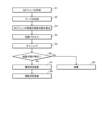
次に、実施の形態1にかかる炭化珪素半導体装置の製造方法について説明する。図4は、実施の形態1にかかる炭化珪素半導体装置の製造方法の概要を示すフローチャートである。
実施の形態2にかかる炭化珪素半導体装置の構造は、実施の形態1(図3)と同じであるため、記載を省略する。また、実施の形態2にかかる炭化珪素半導体装置の製造方法は、実施の形態1にかかる炭化珪素半導体装置の製造方法の概要を示すフローチャート(図4)に対し、ステップS2およびステップS3が異なる。このため、ステップS2およびステップS3のみを説明する。
結晶欠陥検査装置として、SICA装置を用いて結晶欠陥が存在すると判定されたチップに対して、目視で検査したところ、約3割のチップで、結晶欠陥は存在しなかった。この約3割のチップは、SICA装置がマークを線状の結晶欠陥と誤認識したものである。このため、実施の形態による製造方法では、SICA装置による誤認識をほぼなくすことができるため、SICA装置で不良と判定されたチップの約3割を良品にすることができ、良品率を向上させることができる。
2a n型バッファ領域
2b n-型ドリフト領域
3 n型電流拡散領域
4 p型ベース領域
5 n+型ソース領域
6 p++型コンタクト領域
7 トレンチ
8 ゲート絶縁膜
9 ゲート電極
10 炭化珪素半導体装置
11 層間絶縁膜
12 バリアメタル
13 オーミック電極
14 おもて面電極
15 裏面電極
21、22 p+型領域
30 半導体チップ
31、55 n+型出発基板
32 n型エピタキシャル層
33 n-型エピタキシャル層
34 p型エピタキシャル層
35 エピタキシャル層
41 活性領域
42 エッジ終端領域
43 チャネルストッパ部
50、150 半導体ウェハ
51 半導体ウェハのチップ領域
53 半導体ウェハの無効領域
54 オリエンテーションフラット
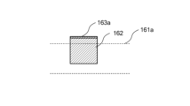
61、161 スクライブライン
61a、61b、161a 結晶欠陥検査装置が認識しているスクライブライン
62、62a、162 マーク
63a、63b、163a マーク端部分
64 線状の結晶欠陥
Claims (5)
- 炭化珪素からなる出発基板上にエピタキシャル層をエピタキシャル成長させてなる半導体ウェハを形成する第1工程と、
前記半導体ウェハに設けられた第1スクライブライン中にマークを形成する第2工程と、
結晶欠陥検査装置により、前記エピタキシャル層を検査して、前記エピタキシャル層の結晶欠陥を検出する第3工程と、
前記半導体ウェハに所定の素子構造を形成する第4工程と、
前記第4工程の後、前記半導体ウェハをダイシングして半導体チップに個片化する第5工程と、
前記第3工程で前記結晶欠陥が検出されなかった前記半導体チップを良品候補として選別する第6工程と、
を含み、
前記結晶欠陥検査装置が認識する第2スクライブラインと前記第1スクライブラインとにずれがない場合の、前記第2スクライブラインの端と前記マークの端との距離を、10μm以上25μm以下とすることを特徴とする炭化珪素半導体装置の製造方法。 - 前記第2スクライブラインの幅を、前記半導体ウェハに設けられた前記第1スクライブラインの幅よりも大きくすることを特徴とする請求項1に記載の炭化珪素半導体装置の製造方法。
- 前記第2スクライブラインの端は、前記半導体チップのチャネルストッパ部に位置することを特徴とする請求項2に記載の炭化珪素半導体装置の製造方法。
- 前記第2スクライブラインの幅は、前記半導体ウェハに設けられた前記第1スクライブラインの幅と同じであることを特徴とする請求項1に記載の炭化珪素半導体装置の製造方法。
- 前記第1スクライブラインは、<11-20>方向と<1-100>方向とに格子状に設けられ、
前記第2スクライブラインと前記第1スクライブラインにずれがない場合の、<11-20>方向の前記第2スクライブラインの端と前記マークの端との距離を、10μm以上25μm以下とすることを特徴とする請求項1に記載の炭化珪素半導体装置の製造方法。
Priority Applications (3)
| Application Number | Priority Date | Filing Date | Title |
|---|---|---|---|
| JP2021083247A JP7697262B2 (ja) | 2021-05-17 | 2021-05-17 | 炭化珪素半導体装置の製造方法 |
| CN202210292108.7A CN115360172A (zh) | 2021-05-17 | 2022-03-23 | 碳化硅半导体装置的制造方法 |
| US17/706,743 US20220367274A1 (en) | 2021-05-17 | 2022-03-29 | Method of manufacturing silicon carbide semiconductor device |
Applications Claiming Priority (1)
| Application Number | Priority Date | Filing Date | Title |
|---|---|---|---|
| JP2021083247A JP7697262B2 (ja) | 2021-05-17 | 2021-05-17 | 炭化珪素半導体装置の製造方法 |
Publications (2)
| Publication Number | Publication Date |
|---|---|
| JP2022176695A JP2022176695A (ja) | 2022-11-30 |
| JP7697262B2 true JP7697262B2 (ja) | 2025-06-24 |
Family
ID=83998017
Family Applications (1)
| Application Number | Title | Priority Date | Filing Date |
|---|---|---|---|
| JP2021083247A Active JP7697262B2 (ja) | 2021-05-17 | 2021-05-17 | 炭化珪素半導体装置の製造方法 |
Country Status (3)
| Country | Link |
|---|---|
| US (1) | US20220367274A1 (ja) |
| JP (1) | JP7697262B2 (ja) |
| CN (1) | CN115360172A (ja) |
Families Citing this family (1)
| Publication number | Priority date | Publication date | Assignee | Title |
|---|---|---|---|---|
| JP7669772B2 (ja) * | 2021-04-15 | 2025-04-30 | 富士電機株式会社 | 炭化珪素半導体装置の製造方法 |
Citations (8)
| Publication number | Priority date | Publication date | Assignee | Title |
|---|---|---|---|---|
| JP2007318030A (ja) | 2006-05-29 | 2007-12-06 | Central Res Inst Of Electric Power Ind | 炭化珪素単結晶の結晶欠陥検査方法および結晶欠陥検査装置 |
| JP2013118242A (ja) | 2011-12-02 | 2013-06-13 | Mitsubishi Electric Corp | 結晶欠陥検出方法、炭化珪素半導体装置の製造方法 |
| JP2013187524A (ja) | 2012-03-12 | 2013-09-19 | Mitsubishi Electric Corp | 欠陥検査方法 |
| JP2013232555A (ja) | 2012-04-27 | 2013-11-14 | Fuji Electric Co Ltd | 半導体装置の製造方法および製造装置 |
| US20140212021A1 (en) | 2013-01-31 | 2014-07-31 | Applied Materials Israel Ltd. | System, a method and a computer program product for patch-based defect detection |
| JP2015126110A (ja) | 2013-12-26 | 2015-07-06 | 住友電気工業株式会社 | 炭化珪素半導体装置の製造方法 |
| JP2015207595A (ja) | 2014-04-17 | 2015-11-19 | 住友電気工業株式会社 | 炭化珪素半導体装置の製造方法 |
| JP2015207596A (ja) | 2014-04-17 | 2015-11-19 | 住友電気工業株式会社 | 炭化珪素半導体装置の製造方法 |
Family Cites Families (6)
| Publication number | Priority date | Publication date | Assignee | Title |
|---|---|---|---|---|
| US5847821A (en) * | 1997-07-10 | 1998-12-08 | Advanced Micro Devices, Inc. | Use of fiducial marks for improved blank wafer defect review |
| JP5980024B2 (ja) * | 2012-07-17 | 2016-08-31 | 三菱電機株式会社 | 炭化珪素半導体装置の製造方法 |
| JP2017055010A (ja) * | 2015-09-11 | 2017-03-16 | 株式会社東芝 | 半導体装置 |
| CN109564882B (zh) * | 2016-08-09 | 2023-08-18 | 三菱电机株式会社 | 半导体装置及其制造方法 |
| DE102020102282B3 (de) * | 2020-01-30 | 2021-04-08 | Infineon Technologies Ag | Halbleitervorrichtung mit ausrichtungspads und verfahren zu deren herstellung |
| WO2022059381A1 (ja) * | 2020-09-16 | 2022-03-24 | ローム株式会社 | 半導体装置の製造方法および半導体装置 |
-
2021
- 2021-05-17 JP JP2021083247A patent/JP7697262B2/ja active Active
-
2022
- 2022-03-23 CN CN202210292108.7A patent/CN115360172A/zh active Pending
- 2022-03-29 US US17/706,743 patent/US20220367274A1/en active Pending
Patent Citations (8)
| Publication number | Priority date | Publication date | Assignee | Title |
|---|---|---|---|---|
| JP2007318030A (ja) | 2006-05-29 | 2007-12-06 | Central Res Inst Of Electric Power Ind | 炭化珪素単結晶の結晶欠陥検査方法および結晶欠陥検査装置 |
| JP2013118242A (ja) | 2011-12-02 | 2013-06-13 | Mitsubishi Electric Corp | 結晶欠陥検出方法、炭化珪素半導体装置の製造方法 |
| JP2013187524A (ja) | 2012-03-12 | 2013-09-19 | Mitsubishi Electric Corp | 欠陥検査方法 |
| JP2013232555A (ja) | 2012-04-27 | 2013-11-14 | Fuji Electric Co Ltd | 半導体装置の製造方法および製造装置 |
| US20140212021A1 (en) | 2013-01-31 | 2014-07-31 | Applied Materials Israel Ltd. | System, a method and a computer program product for patch-based defect detection |
| JP2015126110A (ja) | 2013-12-26 | 2015-07-06 | 住友電気工業株式会社 | 炭化珪素半導体装置の製造方法 |
| JP2015207595A (ja) | 2014-04-17 | 2015-11-19 | 住友電気工業株式会社 | 炭化珪素半導体装置の製造方法 |
| JP2015207596A (ja) | 2014-04-17 | 2015-11-19 | 住友電気工業株式会社 | 炭化珪素半導体装置の製造方法 |
Also Published As
| Publication number | Publication date |
|---|---|
| US20220367274A1 (en) | 2022-11-17 |
| CN115360172A (zh) | 2022-11-18 |
| JP2022176695A (ja) | 2022-11-30 |
Similar Documents
| Publication | Publication Date | Title |
|---|---|---|
| JP6058228B1 (ja) | 半導体装置および半導体装置の製造方法 | |
| JP7230434B2 (ja) | 半導体装置の製造方法 | |
| US10403554B2 (en) | Method for manufacturing semiconductor device | |
| JPWO2009088081A1 (ja) | 半導体装置及びその製造方法 | |
| JP5509543B2 (ja) | 半導体装置の製造方法 | |
| US20120171850A1 (en) | Semiconductor device and method of manufacturing semiconductor device | |
| JP7697262B2 (ja) | 炭化珪素半導体装置の製造方法 | |
| JPWO2018029786A1 (ja) | 半導体装置およびその製造方法 | |
| JP7669787B2 (ja) | 炭化珪素半導体装置および炭化珪素半導体装置の製造方法 | |
| CN109390384B (zh) | 碳化硅半导体装置及碳化硅半导体装置的制造方法 | |
| JP2022176696A (ja) | 炭化珪素半導体装置の製造方法 | |
| US20240405077A1 (en) | Silicon carbide semiconductor device and method of manufacturing silicon carbide semiconductor device | |
| JP7537148B2 (ja) | 半導体装置の製造方法、半導体装置の検査方法および半導体検査装置 | |
| JP7669772B2 (ja) | 炭化珪素半導体装置の製造方法 | |
| JP5332376B2 (ja) | 半導体装置とその製造方法 | |
| JP7805331B2 (ja) | 半導体装置の検査方法、および、半導体装置の製造方法 | |
| JP2014225557A (ja) | 炭化珪素半導体装置および半導体モジュールの製造方法、ならびに炭化珪素半導体装置および半導体モジュール | |
| WO2024075432A1 (ja) | 炭化珪素半導体装置および炭化珪素半導体装置の製造方法 | |
| WO2025126658A1 (ja) | 半導体装置および半導体装置の製造方法 | |
| JP5353036B2 (ja) | 半導体装置の製造方法 | |
| CN118263324A (zh) | 碳化硅mos场效应晶体管及其制造方法 |
Legal Events
| Date | Code | Title | Description |
|---|---|---|---|
| A621 | Written request for application examination |
Free format text: JAPANESE INTERMEDIATE CODE: A621 Effective date: 20240313 |
|
| A977 | Report on retrieval |
Free format text: JAPANESE INTERMEDIATE CODE: A971007 Effective date: 20241219 |
|
| A131 | Notification of reasons for refusal |
Free format text: JAPANESE INTERMEDIATE CODE: A131 Effective date: 20250114 |
|
| A521 | Request for written amendment filed |
Free format text: JAPANESE INTERMEDIATE CODE: A523 Effective date: 20250305 |
|
| TRDD | Decision of grant or rejection written | ||
| A01 | Written decision to grant a patent or to grant a registration (utility model) |
Free format text: JAPANESE INTERMEDIATE CODE: A01 Effective date: 20250513 |
|
| A61 | First payment of annual fees (during grant procedure) |
Free format text: JAPANESE INTERMEDIATE CODE: A61 Effective date: 20250526 |
|
| R150 | Certificate of patent or registration of utility model |
Ref document number: 7697262 Country of ref document: JP Free format text: JAPANESE INTERMEDIATE CODE: R150 |