JP7646397B2 - ディスプレイ装置 - Google Patents
ディスプレイ装置 Download PDFInfo
- Publication number
- JP7646397B2 JP7646397B2 JP2021036692A JP2021036692A JP7646397B2 JP 7646397 B2 JP7646397 B2 JP 7646397B2 JP 2021036692 A JP2021036692 A JP 2021036692A JP 2021036692 A JP2021036692 A JP 2021036692A JP 7646397 B2 JP7646397 B2 JP 7646397B2
- Authority
- JP
- Japan
- Prior art keywords
- pixel
- dam portion
- dam
- display device
- axis direction
- Prior art date
- Legal status (The legal status is an assumption and is not a legal conclusion. Google has not performed a legal analysis and makes no representation as to the accuracy of the status listed.)
- Active
Links
Images


Classifications
-
- G—PHYSICS
- G09—EDUCATION; CRYPTOGRAPHY; DISPLAY; ADVERTISING; SEALS
- G09G—ARRANGEMENTS OR CIRCUITS FOR CONTROL OF INDICATING DEVICES USING STATIC MEANS TO PRESENT VARIABLE INFORMATION
- G09G3/00—Control arrangements or circuits, of interest only in connection with visual indicators other than cathode-ray tubes
- G09G3/20—Control arrangements or circuits, of interest only in connection with visual indicators other than cathode-ray tubes for presentation of an assembly of a number of characters, e.g. a page, by composing the assembly by combination of individual elements arranged in a matrix no fixed position being assigned to or needed to be assigned to the individual characters or partial characters
- G09G3/22—Control arrangements or circuits, of interest only in connection with visual indicators other than cathode-ray tubes for presentation of an assembly of a number of characters, e.g. a page, by composing the assembly by combination of individual elements arranged in a matrix no fixed position being assigned to or needed to be assigned to the individual characters or partial characters using controlled light sources
- G09G3/30—Control arrangements or circuits, of interest only in connection with visual indicators other than cathode-ray tubes for presentation of an assembly of a number of characters, e.g. a page, by composing the assembly by combination of individual elements arranged in a matrix no fixed position being assigned to or needed to be assigned to the individual characters or partial characters using controlled light sources using electroluminescent panels
- G09G3/32—Control arrangements or circuits, of interest only in connection with visual indicators other than cathode-ray tubes for presentation of an assembly of a number of characters, e.g. a page, by composing the assembly by combination of individual elements arranged in a matrix no fixed position being assigned to or needed to be assigned to the individual characters or partial characters using controlled light sources using electroluminescent panels semiconductive, e.g. using light-emitting diodes [LED]
- G09G3/3208—Control arrangements or circuits, of interest only in connection with visual indicators other than cathode-ray tubes for presentation of an assembly of a number of characters, e.g. a page, by composing the assembly by combination of individual elements arranged in a matrix no fixed position being assigned to or needed to be assigned to the individual characters or partial characters using controlled light sources using electroluminescent panels semiconductive, e.g. using light-emitting diodes [LED] organic, e.g. using organic light-emitting diodes [OLED]
- G09G3/3225—Control arrangements or circuits, of interest only in connection with visual indicators other than cathode-ray tubes for presentation of an assembly of a number of characters, e.g. a page, by composing the assembly by combination of individual elements arranged in a matrix no fixed position being assigned to or needed to be assigned to the individual characters or partial characters using controlled light sources using electroluminescent panels semiconductive, e.g. using light-emitting diodes [LED] organic, e.g. using organic light-emitting diodes [OLED] using an active matrix
- G09G3/3233—Control arrangements or circuits, of interest only in connection with visual indicators other than cathode-ray tubes for presentation of an assembly of a number of characters, e.g. a page, by composing the assembly by combination of individual elements arranged in a matrix no fixed position being assigned to or needed to be assigned to the individual characters or partial characters using controlled light sources using electroluminescent panels semiconductive, e.g. using light-emitting diodes [LED] organic, e.g. using organic light-emitting diodes [OLED] using an active matrix with pixel circuitry controlling the current through the light-emitting element
-
- H—ELECTRICITY
- H10—SEMICONDUCTOR DEVICES; ELECTRIC SOLID-STATE DEVICES NOT OTHERWISE PROVIDED FOR
- H10K—ORGANIC ELECTRIC SOLID-STATE DEVICES
- H10K50/00—Organic light-emitting devices
- H10K50/80—Constructional details
- H10K50/84—Passivation; Containers; Encapsulations
- H10K50/842—Containers
- H10K50/8428—Vertical spacers, e.g. arranged between the sealing arrangement and the OLED
-
- H—ELECTRICITY
- H10—SEMICONDUCTOR DEVICES; ELECTRIC SOLID-STATE DEVICES NOT OTHERWISE PROVIDED FOR
- H10K—ORGANIC ELECTRIC SOLID-STATE DEVICES
- H10K59/00—Integrated devices, or assemblies of multiple devices, comprising at least one organic light-emitting element covered by group H10K50/00
- H10K59/10—OLED displays
- H10K59/12—Active-matrix OLED [AMOLED] displays
- H10K59/121—Active-matrix OLED [AMOLED] displays characterised by the geometry or disposition of pixel elements
- H10K59/1213—Active-matrix OLED [AMOLED] displays characterised by the geometry or disposition of pixel elements the pixel elements being TFTs
-
- H—ELECTRICITY
- H10—SEMICONDUCTOR DEVICES; ELECTRIC SOLID-STATE DEVICES NOT OTHERWISE PROVIDED FOR
- H10K—ORGANIC ELECTRIC SOLID-STATE DEVICES
- H10K59/00—Integrated devices, or assemblies of multiple devices, comprising at least one organic light-emitting element covered by group H10K50/00
- H10K59/10—OLED displays
- H10K59/12—Active-matrix OLED [AMOLED] displays
- H10K59/122—Pixel-defining structures or layers, e.g. banks
-
- H—ELECTRICITY
- H10—SEMICONDUCTOR DEVICES; ELECTRIC SOLID-STATE DEVICES NOT OTHERWISE PROVIDED FOR
- H10K—ORGANIC ELECTRIC SOLID-STATE DEVICES
- H10K59/00—Integrated devices, or assemblies of multiple devices, comprising at least one organic light-emitting element covered by group H10K50/00
- H10K59/10—OLED displays
- H10K59/12—Active-matrix OLED [AMOLED] displays
- H10K59/123—Connection of the pixel electrodes to the thin film transistors [TFT]
-
- H—ELECTRICITY
- H10—SEMICONDUCTOR DEVICES; ELECTRIC SOLID-STATE DEVICES NOT OTHERWISE PROVIDED FOR
- H10K—ORGANIC ELECTRIC SOLID-STATE DEVICES
- H10K59/00—Integrated devices, or assemblies of multiple devices, comprising at least one organic light-emitting element covered by group H10K50/00
- H10K59/10—OLED displays
- H10K59/12—Active-matrix OLED [AMOLED] displays
- H10K59/124—Insulating layers formed between TFT elements and OLED elements
-
- H—ELECTRICITY
- H10—SEMICONDUCTOR DEVICES; ELECTRIC SOLID-STATE DEVICES NOT OTHERWISE PROVIDED FOR
- H10K—ORGANIC ELECTRIC SOLID-STATE DEVICES
- H10K59/00—Integrated devices, or assemblies of multiple devices, comprising at least one organic light-emitting element covered by group H10K50/00
- H10K59/30—Devices specially adapted for multicolour light emission
- H10K59/35—Devices specially adapted for multicolour light emission comprising red-green-blue [RGB] subpixels
- H10K59/352—Devices specially adapted for multicolour light emission comprising red-green-blue [RGB] subpixels the areas of the RGB subpixels being different
-
- H—ELECTRICITY
- H10—SEMICONDUCTOR DEVICES; ELECTRIC SOLID-STATE DEVICES NOT OTHERWISE PROVIDED FOR
- H10K—ORGANIC ELECTRIC SOLID-STATE DEVICES
- H10K59/00—Integrated devices, or assemblies of multiple devices, comprising at least one organic light-emitting element covered by group H10K50/00
- H10K59/30—Devices specially adapted for multicolour light emission
- H10K59/35—Devices specially adapted for multicolour light emission comprising red-green-blue [RGB] subpixels
- H10K59/353—Devices specially adapted for multicolour light emission comprising red-green-blue [RGB] subpixels characterised by the geometrical arrangement of the RGB subpixels
-
- G—PHYSICS
- G09—EDUCATION; CRYPTOGRAPHY; DISPLAY; ADVERTISING; SEALS
- G09G—ARRANGEMENTS OR CIRCUITS FOR CONTROL OF INDICATING DEVICES USING STATIC MEANS TO PRESENT VARIABLE INFORMATION
- G09G2300/00—Aspects of the constitution of display devices
- G09G2300/08—Active matrix structure, i.e. with use of active elements, inclusive of non-linear two terminal elements, in the pixels together with light emitting or modulating elements
- G09G2300/0809—Several active elements per pixel in active matrix panels
- G09G2300/0819—Several active elements per pixel in active matrix panels used for counteracting undesired variations, e.g. feedback or autozeroing
-
- G—PHYSICS
- G09—EDUCATION; CRYPTOGRAPHY; DISPLAY; ADVERTISING; SEALS
- G09G—ARRANGEMENTS OR CIRCUITS FOR CONTROL OF INDICATING DEVICES USING STATIC MEANS TO PRESENT VARIABLE INFORMATION
- G09G2300/00—Aspects of the constitution of display devices
- G09G2300/08—Active matrix structure, i.e. with use of active elements, inclusive of non-linear two terminal elements, in the pixels together with light emitting or modulating elements
- G09G2300/0809—Several active elements per pixel in active matrix panels
- G09G2300/0842—Several active elements per pixel in active matrix panels forming a memory circuit, e.g. a dynamic memory with one capacitor
- G09G2300/0861—Several active elements per pixel in active matrix panels forming a memory circuit, e.g. a dynamic memory with one capacitor with additional control of the display period without amending the charge stored in a pixel memory, e.g. by means of additional select electrodes
-
- G—PHYSICS
- G09—EDUCATION; CRYPTOGRAPHY; DISPLAY; ADVERTISING; SEALS
- G09G—ARRANGEMENTS OR CIRCUITS FOR CONTROL OF INDICATING DEVICES USING STATIC MEANS TO PRESENT VARIABLE INFORMATION
- G09G2320/00—Control of display operating conditions
- G09G2320/02—Improving the quality of display appearance
- G09G2320/0238—Improving the black level
-
- G—PHYSICS
- G09—EDUCATION; CRYPTOGRAPHY; DISPLAY; ADVERTISING; SEALS
- G09G—ARRANGEMENTS OR CIRCUITS FOR CONTROL OF INDICATING DEVICES USING STATIC MEANS TO PRESENT VARIABLE INFORMATION
- G09G2330/00—Aspects of power supply; Aspects of display protection and defect management
-
- G—PHYSICS
- G09—EDUCATION; CRYPTOGRAPHY; DISPLAY; ADVERTISING; SEALS
- G09G—ARRANGEMENTS OR CIRCUITS FOR CONTROL OF INDICATING DEVICES USING STATIC MEANS TO PRESENT VARIABLE INFORMATION
- G09G3/00—Control arrangements or circuits, of interest only in connection with visual indicators other than cathode-ray tubes
- G09G3/20—Control arrangements or circuits, of interest only in connection with visual indicators other than cathode-ray tubes for presentation of an assembly of a number of characters, e.g. a page, by composing the assembly by combination of individual elements arranged in a matrix no fixed position being assigned to or needed to be assigned to the individual characters or partial characters
- G09G3/22—Control arrangements or circuits, of interest only in connection with visual indicators other than cathode-ray tubes for presentation of an assembly of a number of characters, e.g. a page, by composing the assembly by combination of individual elements arranged in a matrix no fixed position being assigned to or needed to be assigned to the individual characters or partial characters using controlled light sources
- G09G3/30—Control arrangements or circuits, of interest only in connection with visual indicators other than cathode-ray tubes for presentation of an assembly of a number of characters, e.g. a page, by composing the assembly by combination of individual elements arranged in a matrix no fixed position being assigned to or needed to be assigned to the individual characters or partial characters using controlled light sources using electroluminescent panels
- G09G3/32—Control arrangements or circuits, of interest only in connection with visual indicators other than cathode-ray tubes for presentation of an assembly of a number of characters, e.g. a page, by composing the assembly by combination of individual elements arranged in a matrix no fixed position being assigned to or needed to be assigned to the individual characters or partial characters using controlled light sources using electroluminescent panels semiconductive, e.g. using light-emitting diodes [LED]
- G09G3/3208—Control arrangements or circuits, of interest only in connection with visual indicators other than cathode-ray tubes for presentation of an assembly of a number of characters, e.g. a page, by composing the assembly by combination of individual elements arranged in a matrix no fixed position being assigned to or needed to be assigned to the individual characters or partial characters using controlled light sources using electroluminescent panels semiconductive, e.g. using light-emitting diodes [LED] organic, e.g. using organic light-emitting diodes [OLED]
- G09G3/3225—Control arrangements or circuits, of interest only in connection with visual indicators other than cathode-ray tubes for presentation of an assembly of a number of characters, e.g. a page, by composing the assembly by combination of individual elements arranged in a matrix no fixed position being assigned to or needed to be assigned to the individual characters or partial characters using controlled light sources using electroluminescent panels semiconductive, e.g. using light-emitting diodes [LED] organic, e.g. using organic light-emitting diodes [OLED] using an active matrix
- G09G3/3258—Control arrangements or circuits, of interest only in connection with visual indicators other than cathode-ray tubes for presentation of an assembly of a number of characters, e.g. a page, by composing the assembly by combination of individual elements arranged in a matrix no fixed position being assigned to or needed to be assigned to the individual characters or partial characters using controlled light sources using electroluminescent panels semiconductive, e.g. using light-emitting diodes [LED] organic, e.g. using organic light-emitting diodes [OLED] using an active matrix with pixel circuitry controlling the voltage across the light-emitting element
-
- G—PHYSICS
- G09—EDUCATION; CRYPTOGRAPHY; DISPLAY; ADVERTISING; SEALS
- G09G—ARRANGEMENTS OR CIRCUITS FOR CONTROL OF INDICATING DEVICES USING STATIC MEANS TO PRESENT VARIABLE INFORMATION
- G09G3/00—Control arrangements or circuits, of interest only in connection with visual indicators other than cathode-ray tubes
- G09G3/20—Control arrangements or circuits, of interest only in connection with visual indicators other than cathode-ray tubes for presentation of an assembly of a number of characters, e.g. a page, by composing the assembly by combination of individual elements arranged in a matrix no fixed position being assigned to or needed to be assigned to the individual characters or partial characters
- G09G3/22—Control arrangements or circuits, of interest only in connection with visual indicators other than cathode-ray tubes for presentation of an assembly of a number of characters, e.g. a page, by composing the assembly by combination of individual elements arranged in a matrix no fixed position being assigned to or needed to be assigned to the individual characters or partial characters using controlled light sources
- G09G3/30—Control arrangements or circuits, of interest only in connection with visual indicators other than cathode-ray tubes for presentation of an assembly of a number of characters, e.g. a page, by composing the assembly by combination of individual elements arranged in a matrix no fixed position being assigned to or needed to be assigned to the individual characters or partial characters using controlled light sources using electroluminescent panels
- G09G3/32—Control arrangements or circuits, of interest only in connection with visual indicators other than cathode-ray tubes for presentation of an assembly of a number of characters, e.g. a page, by composing the assembly by combination of individual elements arranged in a matrix no fixed position being assigned to or needed to be assigned to the individual characters or partial characters using controlled light sources using electroluminescent panels semiconductive, e.g. using light-emitting diodes [LED]
- G09G3/3208—Control arrangements or circuits, of interest only in connection with visual indicators other than cathode-ray tubes for presentation of an assembly of a number of characters, e.g. a page, by composing the assembly by combination of individual elements arranged in a matrix no fixed position being assigned to or needed to be assigned to the individual characters or partial characters using controlled light sources using electroluminescent panels semiconductive, e.g. using light-emitting diodes [LED] organic, e.g. using organic light-emitting diodes [OLED]
- G09G3/3266—Details of drivers for scan electrodes
-
- G—PHYSICS
- G09—EDUCATION; CRYPTOGRAPHY; DISPLAY; ADVERTISING; SEALS
- G09G—ARRANGEMENTS OR CIRCUITS FOR CONTROL OF INDICATING DEVICES USING STATIC MEANS TO PRESENT VARIABLE INFORMATION
- G09G3/00—Control arrangements or circuits, of interest only in connection with visual indicators other than cathode-ray tubes
- G09G3/20—Control arrangements or circuits, of interest only in connection with visual indicators other than cathode-ray tubes for presentation of an assembly of a number of characters, e.g. a page, by composing the assembly by combination of individual elements arranged in a matrix no fixed position being assigned to or needed to be assigned to the individual characters or partial characters
- G09G3/22—Control arrangements or circuits, of interest only in connection with visual indicators other than cathode-ray tubes for presentation of an assembly of a number of characters, e.g. a page, by composing the assembly by combination of individual elements arranged in a matrix no fixed position being assigned to or needed to be assigned to the individual characters or partial characters using controlled light sources
- G09G3/30—Control arrangements or circuits, of interest only in connection with visual indicators other than cathode-ray tubes for presentation of an assembly of a number of characters, e.g. a page, by composing the assembly by combination of individual elements arranged in a matrix no fixed position being assigned to or needed to be assigned to the individual characters or partial characters using controlled light sources using electroluminescent panels
- G09G3/32—Control arrangements or circuits, of interest only in connection with visual indicators other than cathode-ray tubes for presentation of an assembly of a number of characters, e.g. a page, by composing the assembly by combination of individual elements arranged in a matrix no fixed position being assigned to or needed to be assigned to the individual characters or partial characters using controlled light sources using electroluminescent panels semiconductive, e.g. using light-emitting diodes [LED]
- G09G3/3208—Control arrangements or circuits, of interest only in connection with visual indicators other than cathode-ray tubes for presentation of an assembly of a number of characters, e.g. a page, by composing the assembly by combination of individual elements arranged in a matrix no fixed position being assigned to or needed to be assigned to the individual characters or partial characters using controlled light sources using electroluminescent panels semiconductive, e.g. using light-emitting diodes [LED] organic, e.g. using organic light-emitting diodes [OLED]
- G09G3/3275—Details of drivers for data electrodes
-
- H—ELECTRICITY
- H10—SEMICONDUCTOR DEVICES; ELECTRIC SOLID-STATE DEVICES NOT OTHERWISE PROVIDED FOR
- H10K—ORGANIC ELECTRIC SOLID-STATE DEVICES
- H10K2102/00—Constructional details relating to the organic devices covered by this subclass
- H10K2102/301—Details of OLEDs
- H10K2102/302—Details of OLEDs of OLED structures
Landscapes
- Engineering & Computer Science (AREA)
- Microelectronics & Electronic Packaging (AREA)
- Physics & Mathematics (AREA)
- Optics & Photonics (AREA)
- Geometry (AREA)
- Computer Hardware Design (AREA)
- General Physics & Mathematics (AREA)
- Theoretical Computer Science (AREA)
- Electroluminescent Light Sources (AREA)
- Devices For Indicating Variable Information By Combining Individual Elements (AREA)
Description
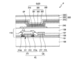
110 画素回路層
210、210R、210G、210B 画素電極
221 第1機能層
222 第2機能層
223、223R、223G、223B 発光層
230 対向電極
240 画素定義膜
PC 画素回路
OLED 有機発光ダイオード
P1、P2、P3 第1画素、第2画素、第3画素
OP1、OP2、OP3 第1開口、第2開口、第3開口
DM1 第1ダム部
DM2 第2ダム部
SDM1 第1サブダム
SDM2 第2サブダム
V バレー
DM1a、DM2a 突出部
Claims (21)
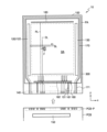
- 基板上に互いに離隔して配置され、互いに異なる色を発光する、第1画素、第2画素、及び第3画素と、
前記第1画素、前記第2画素、及び前記第3画素のそれぞれに対応する開口を含んで発光領域を定義する画素定義膜と、
前記第1画素と前記第2画素との間の前記画素定義膜上に位置した第1ダム部と、
前記第2画素と前記第3画素との間の前記画素定義膜上に位置した第2ダム部と、
前記画素定義膜上に配置されるスペーサと、を備え、
前記第1画素、前記第2画素、及び前記第1ダム部は、第1方向に沿って配置され、前記第2画素、前記第3画素、及び前記第2ダム部は、前記第1方向と交差する第2方向に沿って配置され、
平面上において、前記第1ダム部及び前記第2ダム部のそれぞれは方形であり、
前記第1ダム部の長軸方向は、前記第1方向であり、
前記第2ダム部の長軸方向は、前記第2方向であり、
前記第1ダム部及び前記第2ダム部は、スペーサと同一物質を含む、ディスプレイ装置。 - 基板上に互いに離隔して配置され、互いに異なる色を発光する、第1画素、第2画素、及び第3画素と、
前記第1画素、前記第2画素、及び前記第3画素のそれぞれに対応する開口を含んで発光領域を定義する画素定義膜と、
前記第1画素と前記第2画素との間の前記画素定義膜上に位置した第1ダム部と、
前記第2画素と前記第3画素との間の前記画素定義膜上に位置した第2ダム部と、
前記画素定義膜上に配置されるスペーサと、を備え、
前記第1画素、前記第2画素、及び前記第1ダム部は、第1方向に沿って配置され、前記第2画素、前記第3画素、及び前記第2ダム部は、前記第1方向と交差する第2方向に沿って配置され、
前記第1ダム部及び前記第2ダム部のそれぞれは、第1距離に離隔して配置された第1サブダム及び第2サブダムを含み、
前記第1サブダムと前記第2サブダムとの間に位置するバレー(Valley)をさらに含み、
前記第1ダム部及び前記第2ダム部は、スペーサと同一物質を含む、ディスプレイ装置。 - 基板上に互いに離隔して配置され、互いに異なる色を発光する、第1画素、第2画素、及び第3画素と、
前記第1画素、前記第2画素、及び前記第3画素のそれぞれに対応する開口を含んで発光領域を定義する画素定義膜と、
前記第1画素と前記第2画素との間の前記画素定義膜上に位置した第1ダム部と、
前記第2画素と前記第3画素との間の前記画素定義膜上に位置した第2ダム部と、を備え、
前記第1画素、前記第2画素、及び前記第1ダム部は、第1方向に沿って配置され、前記第2画素、前記第3画素、及び前記第2ダム部は、前記第1方向と交差する第2方向に沿って配置され、
前記第1ダム部の長軸方向は、前記第1方向であり、
前記第1ダム部の短軸方向は、前記第1ダム部の長軸方向と交差する方向であり、
前記第2ダム部の長軸方向は、前記第2方向であり、
前記第2ダム部の短軸方向は、前記第2ダム部の長軸方向と交差する方向であり、
前記第1ダム部は、前記第1ダム部の短軸方向に突出した突出部を含み、
前記第2ダム部は、前記第2ダム部の短軸方向に突出した突出部を含み、
前記第1ダム部の突出部は、前記第1ダム部の短軸方向に沿う1μm以上5μm以下の第3幅を有し、前記第1ダム部の長軸方向に沿う1μm以上5μm以下の第4幅を有する、ディスプレイ装置。 - 前記第1画素と前記第2画素との最短距離は、前記第1画素と前記第3画素との最短距離よりも短い、請求項1~3のいずれか一つに記載のディスプレイ装置。
- 前記第1画素と前記第2画素との最短距離は、17μm未満である、請求項4に記載のディスプレイ装置。
- 前記第1画素と前記第3画素との最短距離は、20μm以上25μm以下である、請求項4に記載のディスプレイ装置。
- 前記第1ダム部及び前記第2ダム部は、前記画素定義膜と同一物質を含んで一体に備えられる、請求項1~3のいずれか一つに記載のディスプレイ装置。
- 前記第1ダム部及び前記第2ダム部は、前記画素定義膜と互いに異なる物質を含む、請求項1~3のいずれか一つに記載のディスプレイ装置。
- 前記第1ダム部及び前記第2ダム部は、逆テーパ状を有する、請求項1~3のいずれか一つに記載のディスプレイ装置。
- 前記第1距離は、1μm以上3μm以下である、請求項2に記載のディスプレイ装置。
- 前記第1ダム部および前記第2ダム部のそれぞれの前記長軸方向は、第1軸方向であって、
前記第1ダム部および前記第2ダム部は、前記第1軸方向に8μm以上12μm以下の第1幅を有し、前記第1軸方向と垂直な第2軸方向に4μm以上8μm以下の第2幅を有する、請求項1または3に記載のディスプレイ装置。 - 前記画素定義膜の前記開口と前記第1ダム部または前記第2ダム部との最短距離は、3μm以下である、請求項1~3のいずれか一つに記載のディスプレイ装置。
- 前記第1画素は、赤色光を発光し、
前記第2画素は、緑光を発光し、
前記第3画素は、青色光を発光する、請求項1~3のいずれか一つに記載のディスプレイ装置。 - 前記第1画素、前記第2画素、及び前記第3画素は、それぞれ複数個備えられ、
前記複数の第1画素及び前記複数の第3画素は、第3方向に沿って交互に配置され、
前記複数の第2画素は、前記第3方向と交差する第4方向に沿って配置される、請求項13に記載のディスプレイ装置。 - 前記第3方向に沿う前記第1ダム部と前記第2ダム部との最短距離は、3μm以下である、請求項14に記載のディスプレイ装置。
- 前記第1ダム部及び前記第2ダム部は、それぞれ複数個備えられ、
前記第4方向に沿う、前記複数の第1ダム部間の最短距離及び前記複数の第2ダム部間の最短距離は、3μm以下である、請求項15に記載のディスプレイ装置。 - 前記第1ダム部及び前記第2ダム部の高さは、2μm以上である、請求項1~3のいずれか一つに記載のディスプレイ装置。
- 前記第1画素は、第1色発光用であり、第1画素電極を有し、
前記第2画素は、第2色発光用であり、第2画素電極を有し、
前記第1画素に対応する開口は、第1開口であって、前記第1画素電極の中央部を露出させ、
前記第2画素に対応する開口は、第2開口であって、前記第2画素電極の中央部を露出させ、
前記第1開口と前記第2開口との最短距離は、17μm未満である、請求項1~3のいずれか一つに記載のディスプレイ装置。 - 前記基板上に配置される第3色発光用第3画素電極と、
前記第2画素電極と前記第3画素電極との間の前記画素定義膜上に配置される第2ダム部と、をさらに含み、
前記第3画素は、前記第3色発光用第3画素電極を有し、
前記画素定義膜は、前記第3画素電極の中央部を露出させる第3開口を有し、
前記第2開口と前記第3開口との最短距離は、17μm未満である、請求項18に記載のディスプレイ装置。 - 前記第1画素電極、前記第1ダム部、及び前記第2画素電極は、前記第1方向に沿って配置され、
前記第2画素電極、前記第2ダム部及び前記第3画素電極は、前記第1方向と交差する第2方向に沿って配置される、請求項19に記載のディスプレイ装置。 - 前記画素定義膜は、前記第1ダム部および前記第2ダム部のいずれから露出する部分を有し、
前記露出する部分の前記基板からの高さは、前記第1ダム部および前記第2ダム部の前記基板からの高さと異なる、請求項1~3のいずれか一つに記載のディスプレイ装置。
Applications Claiming Priority (2)
| Application Number | Priority Date | Filing Date | Title |
|---|---|---|---|
| KR1020200029158A KR20210114094A (ko) | 2020-03-09 | 2020-03-09 | 디스플레이 장치 |
| KR10-2020-0029158 | 2020-03-09 |
Publications (2)
| Publication Number | Publication Date |
|---|---|
| JP2021141067A JP2021141067A (ja) | 2021-09-16 |
| JP7646397B2 true JP7646397B2 (ja) | 2025-03-17 |
Family
ID=77554931
Family Applications (1)
| Application Number | Title | Priority Date | Filing Date |
|---|---|---|---|
| JP2021036692A Active JP7646397B2 (ja) | 2020-03-09 | 2021-03-08 | ディスプレイ装置 |
Country Status (4)
| Country | Link |
|---|---|
| US (2) | US11785807B2 (ja) |
| JP (1) | JP7646397B2 (ja) |
| KR (1) | KR20210114094A (ja) |
| CN (1) | CN113380857A (ja) |
Families Citing this family (10)
| Publication number | Priority date | Publication date | Assignee | Title |
|---|---|---|---|---|
| KR20210114094A (ko) * | 2020-03-09 | 2021-09-23 | 삼성디스플레이 주식회사 | 디스플레이 장치 |
| KR102892748B1 (ko) * | 2022-02-25 | 2025-11-28 | 삼성디스플레이 주식회사 | 표시 장치 |
| US20230345766A1 (en) * | 2022-04-25 | 2023-10-26 | Samsung Display Co., Ltd. | Display device and electronic device including the same |
| KR20240059824A (ko) * | 2022-10-27 | 2024-05-08 | 삼성디스플레이 주식회사 | 표시장치 및 이를 포함하는 전자장치 |
| CN116156947B (zh) * | 2022-12-28 | 2025-11-21 | 武汉天马微电子有限公司 | 显示面板及其制作方法和显示装置 |
| KR20240105832A (ko) * | 2022-12-29 | 2024-07-08 | 엘지디스플레이 주식회사 | 발광표시장치 |
| KR20240107837A (ko) * | 2022-12-30 | 2024-07-09 | 엘지디스플레이 주식회사 | 유기 발광 표시 장치 |
| JP2024099940A (ja) * | 2023-01-13 | 2024-07-26 | セイコーエプソン株式会社 | 表示装置および電子機器 |
| CN120129416A (zh) * | 2023-12-08 | 2025-06-10 | 合肥维信诺科技有限公司 | 显示面板及其制备方法和显示装置 |
| JP7753325B2 (ja) * | 2023-12-13 | 2025-10-14 | エルジー ディスプレイ カンパニー リミテッド | 発光表示装置 |
Citations (10)
| Publication number | Priority date | Publication date | Assignee | Title |
|---|---|---|---|---|
| JP2014216316A (ja) | 2013-04-26 | 2014-11-17 | 三星ディスプレイ株式會社Samsung Display Co.,Ltd. | 有機発光表示装置 |
| US20150162391A1 (en) | 2013-12-10 | 2015-06-11 | Samsung Display Co., Ltd. | Organic light-emitting display apparatus |
| US20160268354A1 (en) | 2015-03-13 | 2016-09-15 | Shanghai Tianma AM-OLED Co., Ltd. | Display panel, display device and manufacturing method of display panel |
| CN106783927A (zh) | 2016-12-28 | 2017-05-31 | 上海天马有机发光显示技术有限公司 | 一种oled显示装置及其制作方法 |
| JP2018049774A (ja) | 2016-09-23 | 2018-03-29 | 株式会社ジャパンディスプレイ | 表示装置 |
| US20180342563A1 (en) | 2017-05-26 | 2018-11-29 | Boe Technology Group Co., Ltd. | Oled display substrate and manufacturing method thereof, display panel and display apparatus |
| JP2019045841A (ja) | 2017-09-05 | 2019-03-22 | 三星ディスプレイ株式會社Samsung Display Co.,Ltd. | 表示装置及びその製造方法 |
| JP2019114526A (ja) | 2018-07-27 | 2019-07-11 | 堺ディスプレイプロダクト株式会社 | 有機el表示装置 |
| CN110098232A (zh) | 2019-04-30 | 2019-08-06 | 深圳市华星光电半导体显示技术有限公司 | Oled显示面板 |
| US20190393415A1 (en) | 2018-06-25 | 2019-12-26 | Samsung Display Co., Ltd. | Organic light-emitting display apparatus and method of manufacturing the same |
Family Cites Families (11)
| Publication number | Priority date | Publication date | Assignee | Title |
|---|---|---|---|---|
| KR20150061921A (ko) * | 2013-11-28 | 2015-06-05 | 엘지디스플레이 주식회사 | 유기전계발광표시장치 |
| JP2016126860A (ja) | 2014-12-26 | 2016-07-11 | ソニー株式会社 | 表示装置、表示装置の製造方法および電子機器 |
| US11043543B2 (en) * | 2015-07-07 | 2021-06-22 | Semiconductor Energy Laboratory Co., Ltd. | Touch sensor and touch panel |
| KR102653000B1 (ko) * | 2016-03-04 | 2024-04-01 | 삼성디스플레이 주식회사 | 유기 발광 표시 장치 및 그 제조 방법 |
| KR102496554B1 (ko) * | 2016-05-25 | 2023-02-08 | 삼성디스플레이 주식회사 | 터치 스크린 패널 |
| US10608062B2 (en) * | 2017-03-16 | 2020-03-31 | Sharp Kabushiki Kaisha | Display device |
| KR102418967B1 (ko) | 2017-10-26 | 2022-07-08 | 삼성디스플레이 주식회사 | 플렉서블 표시 장치 |
| KR102393788B1 (ko) | 2017-11-30 | 2022-05-02 | 엘지디스플레이 주식회사 | 유기발광 표시장치 |
| WO2019130431A1 (ja) * | 2017-12-26 | 2019-07-04 | 堺ディスプレイプロダクト株式会社 | 有機el表示装置およびその製造方法 |
| KR102606941B1 (ko) | 2018-05-31 | 2023-11-30 | 삼성디스플레이 주식회사 | 표시장치 |
| KR20210114094A (ko) * | 2020-03-09 | 2021-09-23 | 삼성디스플레이 주식회사 | 디스플레이 장치 |
-
2020
- 2020-03-09 KR KR1020200029158A patent/KR20210114094A/ko active Pending
- 2020-11-20 US US17/100,521 patent/US11785807B2/en active Active
-
2021
- 2021-03-08 JP JP2021036692A patent/JP7646397B2/ja active Active
- 2021-03-09 CN CN202110256673.3A patent/CN113380857A/zh active Pending
-
2023
- 2023-10-06 US US18/482,837 patent/US12200978B2/en active Active
Patent Citations (10)
| Publication number | Priority date | Publication date | Assignee | Title |
|---|---|---|---|---|
| JP2014216316A (ja) | 2013-04-26 | 2014-11-17 | 三星ディスプレイ株式會社Samsung Display Co.,Ltd. | 有機発光表示装置 |
| US20150162391A1 (en) | 2013-12-10 | 2015-06-11 | Samsung Display Co., Ltd. | Organic light-emitting display apparatus |
| US20160268354A1 (en) | 2015-03-13 | 2016-09-15 | Shanghai Tianma AM-OLED Co., Ltd. | Display panel, display device and manufacturing method of display panel |
| JP2018049774A (ja) | 2016-09-23 | 2018-03-29 | 株式会社ジャパンディスプレイ | 表示装置 |
| CN106783927A (zh) | 2016-12-28 | 2017-05-31 | 上海天马有机发光显示技术有限公司 | 一种oled显示装置及其制作方法 |
| US20180342563A1 (en) | 2017-05-26 | 2018-11-29 | Boe Technology Group Co., Ltd. | Oled display substrate and manufacturing method thereof, display panel and display apparatus |
| JP2019045841A (ja) | 2017-09-05 | 2019-03-22 | 三星ディスプレイ株式會社Samsung Display Co.,Ltd. | 表示装置及びその製造方法 |
| US20190393415A1 (en) | 2018-06-25 | 2019-12-26 | Samsung Display Co., Ltd. | Organic light-emitting display apparatus and method of manufacturing the same |
| JP2019114526A (ja) | 2018-07-27 | 2019-07-11 | 堺ディスプレイプロダクト株式会社 | 有機el表示装置 |
| CN110098232A (zh) | 2019-04-30 | 2019-08-06 | 深圳市华星光电半导体显示技术有限公司 | Oled显示面板 |
Also Published As
| Publication number | Publication date |
|---|---|
| JP2021141067A (ja) | 2021-09-16 |
| US20210280647A1 (en) | 2021-09-09 |
| US20240040852A1 (en) | 2024-02-01 |
| US11785807B2 (en) | 2023-10-10 |
| CN113380857A (zh) | 2021-09-10 |
| KR20210114094A (ko) | 2021-09-23 |
| US12200978B2 (en) | 2025-01-14 |
Similar Documents
| Publication | Publication Date | Title |
|---|---|---|
| JP7646397B2 (ja) | ディスプレイ装置 | |
| JP7803995B2 (ja) | 表示装置の製造装置 | |
| US20210335948A1 (en) | Display device | |
| JP7534132B2 (ja) | 表示装置及び表示装置の製造方法 | |
| US12002429B2 (en) | Display panel and display apparatus including the same | |
| KR102906644B1 (ko) | 디스플레이 장치 | |
| KR102578834B1 (ko) | 유기 발광 표시 장치 | |
| KR102769670B1 (ko) | 유기 발광 표시 장치 | |
| US12484421B2 (en) | Display apparatus including multi-layered second encapsulation layer | |
| JP7376597B2 (ja) | ディスプレイ装置 | |
| CN113013196B (zh) | 显示面板和包括该显示面板的显示设备 | |
| KR102712663B1 (ko) | 표시 장치 | |
| KR20170114028A (ko) | 표시 장치 | |
| JP7564684B2 (ja) | 有機発光表示装置 | |
| KR20200046223A (ko) | 디스플레이 장치 | |
| CN113555393A (zh) | 显示装置 | |
| KR102591727B1 (ko) | 정전기 방지 다이오드 및 정전기 방지 구조물을 포함하는 유기 발광 표시 장치 | |
| CN121442917A (zh) | 有机发光显示设备 | |
| US20220165804A1 (en) | Display apparatus | |
| KR102886841B1 (ko) | 표시 장치 | |
| US11869421B2 (en) | Display device | |
| KR20240023279A (ko) | 표시패널 및 이를 구비하는 표시장치 | |
| CN116390578A (zh) | 有机发光显示装置及其制造方法 | |
| CN118613084A (zh) | 显示面板及显示装置 | |
| KR20240043224A (ko) | 디스플레이 장치 |
Legal Events
| Date | Code | Title | Description |
|---|---|---|---|
| A621 | Written request for application examination |
Free format text: JAPANESE INTERMEDIATE CODE: A621 Effective date: 20240112 |
|
| A977 | Report on retrieval |
Free format text: JAPANESE INTERMEDIATE CODE: A971007 Effective date: 20240711 |
|
| A131 | Notification of reasons for refusal |
Free format text: JAPANESE INTERMEDIATE CODE: A131 Effective date: 20240730 |
|
| A521 | Request for written amendment filed |
Free format text: JAPANESE INTERMEDIATE CODE: A523 Effective date: 20241030 |
|
| TRDD | Decision of grant or rejection written | ||
| A01 | Written decision to grant a patent or to grant a registration (utility model) |
Free format text: JAPANESE INTERMEDIATE CODE: A01 Effective date: 20250204 |
|
| A61 | First payment of annual fees (during grant procedure) |
Free format text: JAPANESE INTERMEDIATE CODE: A61 Effective date: 20250305 |
|
| R150 | Certificate of patent or registration of utility model |
Ref document number: 7646397 Country of ref document: JP Free format text: JAPANESE INTERMEDIATE CODE: R150 |