JP7646397B2 - Display device - Google Patents
Display device Download PDFInfo
- Publication number
- JP7646397B2 JP7646397B2 JP2021036692A JP2021036692A JP7646397B2 JP 7646397 B2 JP7646397 B2 JP 7646397B2 JP 2021036692 A JP2021036692 A JP 2021036692A JP 2021036692 A JP2021036692 A JP 2021036692A JP 7646397 B2 JP7646397 B2 JP 7646397B2
- Authority
- JP
- Japan
- Prior art keywords
- pixel
- dam portion
- dam
- display device
- axis direction
- Prior art date
- Legal status (The legal status is an assumption and is not a legal conclusion. Google has not performed a legal analysis and makes no representation as to the accuracy of the status listed.)
- Active
Links
Images


Classifications
-
- G—PHYSICS
- G09—EDUCATION; CRYPTOGRAPHY; DISPLAY; ADVERTISING; SEALS
- G09G—ARRANGEMENTS OR CIRCUITS FOR CONTROL OF INDICATING DEVICES USING STATIC MEANS TO PRESENT VARIABLE INFORMATION
- G09G3/00—Control arrangements or circuits, of interest only in connection with visual indicators other than cathode-ray tubes
- G09G3/20—Control arrangements or circuits, of interest only in connection with visual indicators other than cathode-ray tubes for presentation of an assembly of a number of characters, e.g. a page, by composing the assembly by combination of individual elements arranged in a matrix no fixed position being assigned to or needed to be assigned to the individual characters or partial characters
- G09G3/22—Control arrangements or circuits, of interest only in connection with visual indicators other than cathode-ray tubes for presentation of an assembly of a number of characters, e.g. a page, by composing the assembly by combination of individual elements arranged in a matrix no fixed position being assigned to or needed to be assigned to the individual characters or partial characters using controlled light sources
- G09G3/30—Control arrangements or circuits, of interest only in connection with visual indicators other than cathode-ray tubes for presentation of an assembly of a number of characters, e.g. a page, by composing the assembly by combination of individual elements arranged in a matrix no fixed position being assigned to or needed to be assigned to the individual characters or partial characters using controlled light sources using electroluminescent panels
- G09G3/32—Control arrangements or circuits, of interest only in connection with visual indicators other than cathode-ray tubes for presentation of an assembly of a number of characters, e.g. a page, by composing the assembly by combination of individual elements arranged in a matrix no fixed position being assigned to or needed to be assigned to the individual characters or partial characters using controlled light sources using electroluminescent panels semiconductive, e.g. using light-emitting diodes [LED]
- G09G3/3208—Control arrangements or circuits, of interest only in connection with visual indicators other than cathode-ray tubes for presentation of an assembly of a number of characters, e.g. a page, by composing the assembly by combination of individual elements arranged in a matrix no fixed position being assigned to or needed to be assigned to the individual characters or partial characters using controlled light sources using electroluminescent panels semiconductive, e.g. using light-emitting diodes [LED] organic, e.g. using organic light-emitting diodes [OLED]
- G09G3/3225—Control arrangements or circuits, of interest only in connection with visual indicators other than cathode-ray tubes for presentation of an assembly of a number of characters, e.g. a page, by composing the assembly by combination of individual elements arranged in a matrix no fixed position being assigned to or needed to be assigned to the individual characters or partial characters using controlled light sources using electroluminescent panels semiconductive, e.g. using light-emitting diodes [LED] organic, e.g. using organic light-emitting diodes [OLED] using an active matrix
- G09G3/3233—Control arrangements or circuits, of interest only in connection with visual indicators other than cathode-ray tubes for presentation of an assembly of a number of characters, e.g. a page, by composing the assembly by combination of individual elements arranged in a matrix no fixed position being assigned to or needed to be assigned to the individual characters or partial characters using controlled light sources using electroluminescent panels semiconductive, e.g. using light-emitting diodes [LED] organic, e.g. using organic light-emitting diodes [OLED] using an active matrix with pixel circuitry controlling the current through the light-emitting element
-
- H—ELECTRICITY
- H10—SEMICONDUCTOR DEVICES; ELECTRIC SOLID-STATE DEVICES NOT OTHERWISE PROVIDED FOR
- H10K—ORGANIC ELECTRIC SOLID-STATE DEVICES
- H10K50/00—Organic light-emitting devices
- H10K50/80—Constructional details
- H10K50/84—Passivation; Containers; Encapsulations
- H10K50/842—Containers
- H10K50/8428—Vertical spacers, e.g. arranged between the sealing arrangement and the OLED
-
- H—ELECTRICITY
- H10—SEMICONDUCTOR DEVICES; ELECTRIC SOLID-STATE DEVICES NOT OTHERWISE PROVIDED FOR
- H10K—ORGANIC ELECTRIC SOLID-STATE DEVICES
- H10K59/00—Integrated devices, or assemblies of multiple devices, comprising at least one organic light-emitting element covered by group H10K50/00
- H10K59/10—OLED displays
- H10K59/12—Active-matrix OLED [AMOLED] displays
- H10K59/121—Active-matrix OLED [AMOLED] displays characterised by the geometry or disposition of pixel elements
- H10K59/1213—Active-matrix OLED [AMOLED] displays characterised by the geometry or disposition of pixel elements the pixel elements being TFTs
-
- H—ELECTRICITY
- H10—SEMICONDUCTOR DEVICES; ELECTRIC SOLID-STATE DEVICES NOT OTHERWISE PROVIDED FOR
- H10K—ORGANIC ELECTRIC SOLID-STATE DEVICES
- H10K59/00—Integrated devices, or assemblies of multiple devices, comprising at least one organic light-emitting element covered by group H10K50/00
- H10K59/10—OLED displays
- H10K59/12—Active-matrix OLED [AMOLED] displays
- H10K59/122—Pixel-defining structures or layers, e.g. banks
-
- H—ELECTRICITY
- H10—SEMICONDUCTOR DEVICES; ELECTRIC SOLID-STATE DEVICES NOT OTHERWISE PROVIDED FOR
- H10K—ORGANIC ELECTRIC SOLID-STATE DEVICES
- H10K59/00—Integrated devices, or assemblies of multiple devices, comprising at least one organic light-emitting element covered by group H10K50/00
- H10K59/10—OLED displays
- H10K59/12—Active-matrix OLED [AMOLED] displays
- H10K59/123—Connection of the pixel electrodes to the thin film transistors [TFT]
-
- H—ELECTRICITY
- H10—SEMICONDUCTOR DEVICES; ELECTRIC SOLID-STATE DEVICES NOT OTHERWISE PROVIDED FOR
- H10K—ORGANIC ELECTRIC SOLID-STATE DEVICES
- H10K59/00—Integrated devices, or assemblies of multiple devices, comprising at least one organic light-emitting element covered by group H10K50/00
- H10K59/10—OLED displays
- H10K59/12—Active-matrix OLED [AMOLED] displays
- H10K59/124—Insulating layers formed between TFT elements and OLED elements
-
- H—ELECTRICITY
- H10—SEMICONDUCTOR DEVICES; ELECTRIC SOLID-STATE DEVICES NOT OTHERWISE PROVIDED FOR
- H10K—ORGANIC ELECTRIC SOLID-STATE DEVICES
- H10K59/00—Integrated devices, or assemblies of multiple devices, comprising at least one organic light-emitting element covered by group H10K50/00
- H10K59/30—Devices specially adapted for multicolour light emission
- H10K59/35—Devices specially adapted for multicolour light emission comprising red-green-blue [RGB] subpixels
- H10K59/352—Devices specially adapted for multicolour light emission comprising red-green-blue [RGB] subpixels the areas of the RGB subpixels being different
-
- H—ELECTRICITY
- H10—SEMICONDUCTOR DEVICES; ELECTRIC SOLID-STATE DEVICES NOT OTHERWISE PROVIDED FOR
- H10K—ORGANIC ELECTRIC SOLID-STATE DEVICES
- H10K59/00—Integrated devices, or assemblies of multiple devices, comprising at least one organic light-emitting element covered by group H10K50/00
- H10K59/30—Devices specially adapted for multicolour light emission
- H10K59/35—Devices specially adapted for multicolour light emission comprising red-green-blue [RGB] subpixels
- H10K59/353—Devices specially adapted for multicolour light emission comprising red-green-blue [RGB] subpixels characterised by the geometrical arrangement of the RGB subpixels
-
- G—PHYSICS
- G09—EDUCATION; CRYPTOGRAPHY; DISPLAY; ADVERTISING; SEALS
- G09G—ARRANGEMENTS OR CIRCUITS FOR CONTROL OF INDICATING DEVICES USING STATIC MEANS TO PRESENT VARIABLE INFORMATION
- G09G2300/00—Aspects of the constitution of display devices
- G09G2300/08—Active matrix structure, i.e. with use of active elements, inclusive of non-linear two terminal elements, in the pixels together with light emitting or modulating elements
- G09G2300/0809—Several active elements per pixel in active matrix panels
- G09G2300/0819—Several active elements per pixel in active matrix panels used for counteracting undesired variations, e.g. feedback or autozeroing
-
- G—PHYSICS
- G09—EDUCATION; CRYPTOGRAPHY; DISPLAY; ADVERTISING; SEALS
- G09G—ARRANGEMENTS OR CIRCUITS FOR CONTROL OF INDICATING DEVICES USING STATIC MEANS TO PRESENT VARIABLE INFORMATION
- G09G2300/00—Aspects of the constitution of display devices
- G09G2300/08—Active matrix structure, i.e. with use of active elements, inclusive of non-linear two terminal elements, in the pixels together with light emitting or modulating elements
- G09G2300/0809—Several active elements per pixel in active matrix panels
- G09G2300/0842—Several active elements per pixel in active matrix panels forming a memory circuit, e.g. a dynamic memory with one capacitor
- G09G2300/0861—Several active elements per pixel in active matrix panels forming a memory circuit, e.g. a dynamic memory with one capacitor with additional control of the display period without amending the charge stored in a pixel memory, e.g. by means of additional select electrodes
-
- G—PHYSICS
- G09—EDUCATION; CRYPTOGRAPHY; DISPLAY; ADVERTISING; SEALS
- G09G—ARRANGEMENTS OR CIRCUITS FOR CONTROL OF INDICATING DEVICES USING STATIC MEANS TO PRESENT VARIABLE INFORMATION
- G09G2320/00—Control of display operating conditions
- G09G2320/02—Improving the quality of display appearance
- G09G2320/0238—Improving the black level
-
- G—PHYSICS
- G09—EDUCATION; CRYPTOGRAPHY; DISPLAY; ADVERTISING; SEALS
- G09G—ARRANGEMENTS OR CIRCUITS FOR CONTROL OF INDICATING DEVICES USING STATIC MEANS TO PRESENT VARIABLE INFORMATION
- G09G2330/00—Aspects of power supply; Aspects of display protection and defect management
-
- G—PHYSICS
- G09—EDUCATION; CRYPTOGRAPHY; DISPLAY; ADVERTISING; SEALS
- G09G—ARRANGEMENTS OR CIRCUITS FOR CONTROL OF INDICATING DEVICES USING STATIC MEANS TO PRESENT VARIABLE INFORMATION
- G09G3/00—Control arrangements or circuits, of interest only in connection with visual indicators other than cathode-ray tubes
- G09G3/20—Control arrangements or circuits, of interest only in connection with visual indicators other than cathode-ray tubes for presentation of an assembly of a number of characters, e.g. a page, by composing the assembly by combination of individual elements arranged in a matrix no fixed position being assigned to or needed to be assigned to the individual characters or partial characters
- G09G3/22—Control arrangements or circuits, of interest only in connection with visual indicators other than cathode-ray tubes for presentation of an assembly of a number of characters, e.g. a page, by composing the assembly by combination of individual elements arranged in a matrix no fixed position being assigned to or needed to be assigned to the individual characters or partial characters using controlled light sources
- G09G3/30—Control arrangements or circuits, of interest only in connection with visual indicators other than cathode-ray tubes for presentation of an assembly of a number of characters, e.g. a page, by composing the assembly by combination of individual elements arranged in a matrix no fixed position being assigned to or needed to be assigned to the individual characters or partial characters using controlled light sources using electroluminescent panels
- G09G3/32—Control arrangements or circuits, of interest only in connection with visual indicators other than cathode-ray tubes for presentation of an assembly of a number of characters, e.g. a page, by composing the assembly by combination of individual elements arranged in a matrix no fixed position being assigned to or needed to be assigned to the individual characters or partial characters using controlled light sources using electroluminescent panels semiconductive, e.g. using light-emitting diodes [LED]
- G09G3/3208—Control arrangements or circuits, of interest only in connection with visual indicators other than cathode-ray tubes for presentation of an assembly of a number of characters, e.g. a page, by composing the assembly by combination of individual elements arranged in a matrix no fixed position being assigned to or needed to be assigned to the individual characters or partial characters using controlled light sources using electroluminescent panels semiconductive, e.g. using light-emitting diodes [LED] organic, e.g. using organic light-emitting diodes [OLED]
- G09G3/3225—Control arrangements or circuits, of interest only in connection with visual indicators other than cathode-ray tubes for presentation of an assembly of a number of characters, e.g. a page, by composing the assembly by combination of individual elements arranged in a matrix no fixed position being assigned to or needed to be assigned to the individual characters or partial characters using controlled light sources using electroluminescent panels semiconductive, e.g. using light-emitting diodes [LED] organic, e.g. using organic light-emitting diodes [OLED] using an active matrix
- G09G3/3258—Control arrangements or circuits, of interest only in connection with visual indicators other than cathode-ray tubes for presentation of an assembly of a number of characters, e.g. a page, by composing the assembly by combination of individual elements arranged in a matrix no fixed position being assigned to or needed to be assigned to the individual characters or partial characters using controlled light sources using electroluminescent panels semiconductive, e.g. using light-emitting diodes [LED] organic, e.g. using organic light-emitting diodes [OLED] using an active matrix with pixel circuitry controlling the voltage across the light-emitting element
-
- G—PHYSICS
- G09—EDUCATION; CRYPTOGRAPHY; DISPLAY; ADVERTISING; SEALS
- G09G—ARRANGEMENTS OR CIRCUITS FOR CONTROL OF INDICATING DEVICES USING STATIC MEANS TO PRESENT VARIABLE INFORMATION
- G09G3/00—Control arrangements or circuits, of interest only in connection with visual indicators other than cathode-ray tubes
- G09G3/20—Control arrangements or circuits, of interest only in connection with visual indicators other than cathode-ray tubes for presentation of an assembly of a number of characters, e.g. a page, by composing the assembly by combination of individual elements arranged in a matrix no fixed position being assigned to or needed to be assigned to the individual characters or partial characters
- G09G3/22—Control arrangements or circuits, of interest only in connection with visual indicators other than cathode-ray tubes for presentation of an assembly of a number of characters, e.g. a page, by composing the assembly by combination of individual elements arranged in a matrix no fixed position being assigned to or needed to be assigned to the individual characters or partial characters using controlled light sources
- G09G3/30—Control arrangements or circuits, of interest only in connection with visual indicators other than cathode-ray tubes for presentation of an assembly of a number of characters, e.g. a page, by composing the assembly by combination of individual elements arranged in a matrix no fixed position being assigned to or needed to be assigned to the individual characters or partial characters using controlled light sources using electroluminescent panels
- G09G3/32—Control arrangements or circuits, of interest only in connection with visual indicators other than cathode-ray tubes for presentation of an assembly of a number of characters, e.g. a page, by composing the assembly by combination of individual elements arranged in a matrix no fixed position being assigned to or needed to be assigned to the individual characters or partial characters using controlled light sources using electroluminescent panels semiconductive, e.g. using light-emitting diodes [LED]
- G09G3/3208—Control arrangements or circuits, of interest only in connection with visual indicators other than cathode-ray tubes for presentation of an assembly of a number of characters, e.g. a page, by composing the assembly by combination of individual elements arranged in a matrix no fixed position being assigned to or needed to be assigned to the individual characters or partial characters using controlled light sources using electroluminescent panels semiconductive, e.g. using light-emitting diodes [LED] organic, e.g. using organic light-emitting diodes [OLED]
- G09G3/3266—Details of drivers for scan electrodes
-
- G—PHYSICS
- G09—EDUCATION; CRYPTOGRAPHY; DISPLAY; ADVERTISING; SEALS
- G09G—ARRANGEMENTS OR CIRCUITS FOR CONTROL OF INDICATING DEVICES USING STATIC MEANS TO PRESENT VARIABLE INFORMATION
- G09G3/00—Control arrangements or circuits, of interest only in connection with visual indicators other than cathode-ray tubes
- G09G3/20—Control arrangements or circuits, of interest only in connection with visual indicators other than cathode-ray tubes for presentation of an assembly of a number of characters, e.g. a page, by composing the assembly by combination of individual elements arranged in a matrix no fixed position being assigned to or needed to be assigned to the individual characters or partial characters
- G09G3/22—Control arrangements or circuits, of interest only in connection with visual indicators other than cathode-ray tubes for presentation of an assembly of a number of characters, e.g. a page, by composing the assembly by combination of individual elements arranged in a matrix no fixed position being assigned to or needed to be assigned to the individual characters or partial characters using controlled light sources
- G09G3/30—Control arrangements or circuits, of interest only in connection with visual indicators other than cathode-ray tubes for presentation of an assembly of a number of characters, e.g. a page, by composing the assembly by combination of individual elements arranged in a matrix no fixed position being assigned to or needed to be assigned to the individual characters or partial characters using controlled light sources using electroluminescent panels
- G09G3/32—Control arrangements or circuits, of interest only in connection with visual indicators other than cathode-ray tubes for presentation of an assembly of a number of characters, e.g. a page, by composing the assembly by combination of individual elements arranged in a matrix no fixed position being assigned to or needed to be assigned to the individual characters or partial characters using controlled light sources using electroluminescent panels semiconductive, e.g. using light-emitting diodes [LED]
- G09G3/3208—Control arrangements or circuits, of interest only in connection with visual indicators other than cathode-ray tubes for presentation of an assembly of a number of characters, e.g. a page, by composing the assembly by combination of individual elements arranged in a matrix no fixed position being assigned to or needed to be assigned to the individual characters or partial characters using controlled light sources using electroluminescent panels semiconductive, e.g. using light-emitting diodes [LED] organic, e.g. using organic light-emitting diodes [OLED]
- G09G3/3275—Details of drivers for data electrodes
-
- H—ELECTRICITY
- H10—SEMICONDUCTOR DEVICES; ELECTRIC SOLID-STATE DEVICES NOT OTHERWISE PROVIDED FOR
- H10K—ORGANIC ELECTRIC SOLID-STATE DEVICES
- H10K2102/00—Constructional details relating to the organic devices covered by this subclass
- H10K2102/301—Details of OLEDs
- H10K2102/302—Details of OLEDs of OLED structures
Landscapes
- Engineering & Computer Science (AREA)
- Microelectronics & Electronic Packaging (AREA)
- Physics & Mathematics (AREA)
- Optics & Photonics (AREA)
- Geometry (AREA)
- Computer Hardware Design (AREA)
- General Physics & Mathematics (AREA)
- Theoretical Computer Science (AREA)
- Electroluminescent Light Sources (AREA)
- Devices For Indicating Variable Information By Combining Individual Elements (AREA)
Description
本発明は、ディスプレイ装置に係り、さらに詳細には、高解像度において画質が改善されたディスプレイ装置に関する。 The present invention relates to a display device, and more particularly to a display device with improved image quality at high resolution.
最近、ディスプレイ装置は、その用途が多様化されている。また、ディスプレイ装置の軽量化及び薄板化によって、その使用範囲が広範囲になっている傾向にある。 Recently, the uses of display devices have become more diverse. In addition, as display devices have become lighter and thinner, the range of their use is becoming more widespread.
ディスプレイ装置において、有機発光ディスプレイ装置は、視野角が広く、コントラスト(contrast)に優れ、かつ応答速度が速いという長所を有しており、次世代ディスプレイ装置として脚光を浴びている。 Among display devices, organic light-emitting display devices have the advantages of a wide viewing angle, excellent contrast, and fast response speed, and are in the spotlight as the next-generation display device.
一般に、有機発光ディスプレイ装置は、基板上に薄膜トランジスタ及び有機発光素子を形成し、有機発光素子が自ら発光して作動する。そのような有機発光ディスプレイ装置は、携帯電話のような小型製品のディスプレイ部で使用されたり、テレビのような大型製品のディスプレイ部で使用されたりもする。 In general, an organic light-emitting display device is formed by forming thin film transistors and organic light-emitting elements on a substrate, and the organic light-emitting elements emit light by themselves. Such organic light-emitting display devices are used in the display section of small products such as mobile phones, and in the display section of large products such as televisions.
しかし、そのような従来のディスプレイ装置は、解像度が高くなるにつれて、画素間距離が短くなり、画素間に混色が発生するという問題点が存在した。 However, such conventional display devices had the problem that as the resolution increased, the distance between pixels became shorter, resulting in color mixing between pixels.
本発明は、前記のような問題点を含め、多くの問題点を解決するためのものであって、高解像度において画質が改善されたディスプレイ装置を提供することを目的とする。しかし、このような課題は、例示的なものであって、これにより、本発明の範囲が限定されるものではない。 The present invention is intended to solve many problems, including those mentioned above, and aims to provide a display device with improved image quality at high resolution. However, these problems are merely examples and do not limit the scope of the present invention.
本発明の一観点によれば、基板上に互いに離隔して配置され、互いに異なる色を発光する第1画素、第2画素、及び第3画素と、前記第1画素、前記第2画素、及び前記第3画素のそれぞれに対応する開口を含んで発光領域を定義する画素定義膜と、前記第1画素と前記第2画素との間の前記画素定義膜上に位置した第1ダム部と、前記第2画素と前記第3画素との間の前記画素定義膜上に位置した第2ダム部と、を備える、ディスプレイ装置が提供される。 According to one aspect of the present invention, a display device is provided that includes a first pixel, a second pixel, and a third pixel that are spaced apart from each other on a substrate and emit different colors from each other; a pixel definition film that defines a light-emitting region including openings corresponding to the first pixel, the second pixel, and the third pixel; a first dam portion located on the pixel definition film between the first pixel and the second pixel; and a second dam portion located on the pixel definition film between the second pixel and the third pixel.
本実施例によれば、前記第1画素、前記第2画素、及び前記第1ダム部は、第1方向に沿って配置され、前記第2画素、前記第3画素、及び前記第2ダム部は、前記第1方向と交差する第2方向に沿って配置されうる。 According to this embodiment, the first pixel, the second pixel, and the first dam portion may be arranged along a first direction, and the second pixel, the third pixel, and the second dam portion may be arranged along a second direction that intersects with the first direction.
本実施例によれば、前記第1画素と前記第2画素との最短距離は、前記第1画素と前記第3画素との最短距離よりも短い。 In this embodiment, the shortest distance between the first pixel and the second pixel is shorter than the shortest distance between the first pixel and the third pixel.
本実施例によれば、前記第1画素と前記第2画素との最短距離は、17μm未満であってもよい。 According to this embodiment, the shortest distance between the first pixel and the second pixel may be less than 17 μm.
本実施例によれば、前記第1画素と前記第3画素との最短距離は、20μm以上25μm以下であってもよい。 According to this embodiment, the shortest distance between the first pixel and the third pixel may be greater than or equal to 20 μm and less than or equal to 25 μm.
本実施例によれば、前記第1ダム部及び前記第2ダム部は、前記画素定義膜と同一物質を含んで一体に備えられてもよい。 According to this embodiment, the first dam portion and the second dam portion may be integrally formed with the pixel defining film by containing the same material.
本実施例によれば、前記第1ダム部及び前記第2ダム部は、前記画素定義膜と互いに異なる物質を含んでもよい。 According to this embodiment, the first dam portion and the second dam portion may include a material different from that of the pixel defining film.
本実施例によれば、前記画素定義膜上に配置されるスペーサをさらに含み、前記第1ダム部及び前記第2ダム部は、スペーサと同一物質を含んでもよい。 According to this embodiment, the pixel defining film may further include a spacer disposed on the pixel defining film, and the first dam portion and the second dam portion may include the same material as the spacer.
本実施例によれば、前記第1ダム部及び前記第2ダム部は、逆テーパ状を有してもよい。 According to this embodiment, the first dam portion and the second dam portion may have an inverted tapered shape.
本実施例によれば、前記第1ダム部及び前記第2ダム部のそれぞれは、第1距離に離隔して配置された第1サブダム及び第2サブダムを含んでもよい。 According to this embodiment, each of the first dam section and the second dam section may include a first sub-dam and a second sub-dam spaced a first distance apart.
本実施例によれば、前記第1距離は、1μm以上3μm以下であってもよい。 According to this embodiment, the first distance may be greater than or equal to 1 μm and less than or equal to 3 μm.
本実施例によれば、前記第1サブダムと前記第2サブダムとの間に位置するバレー(Valley)をさらに含んでもよい。 According to this embodiment, the dam may further include a valley located between the first sub-dam and the second sub-dam.
本実施例によれば、平面上において、前記第1ダム部及び前記第2ダム部のそれぞれは方形であり、第1軸方向に8μm以上12μm以下の第1幅を有し、前記第1軸と垂直な第2軸方向に4μm以上8μm以下の第2幅を有してもよい。 According to this embodiment, in a plane, each of the first dam portion and the second dam portion may be rectangular, have a first width of 8 μm or more and 12 μm or less in a first axis direction, and have a second width of 4 μm or more and 8 μm or less in a second axis direction perpendicular to the first axis.
本実施例によれば、前記画素定義膜の前記開口と前記第1ダム部または前記第2ダム部との最短距離は、3μm以下であってもよい。 According to this embodiment, the shortest distance between the opening in the pixel definition film and the first dam portion or the second dam portion may be 3 μm or less.
本実施例によれば、前記第1画素は、赤色光を発光し、前記第2画素は、緑光を発光し、前記第3画素は、青色光を発光することができる。 According to this embodiment, the first pixel can emit red light, the second pixel can emit green light, and the third pixel can emit blue light.
本実施例によれば、前記第1画素、前記第2画素、及び前記第3画素は、それぞれ複数個備えられ、前記複数の第1画素及び前記複数の第2画素は、第3方向に沿って交互に配置され、前記複数の第2画素は、前記第3方向と交差する第4方向に沿って配置されうる。 According to this embodiment, the first pixel, the second pixel, and the third pixel are each provided in multiples, the multiple first pixels and the multiple second pixels are alternately arranged along a third direction, and the multiple second pixels are arranged along a fourth direction intersecting the third direction.
本実施例によれば、前記第3方向に沿う前記第1ダム部と前記第2ダム部との最短距離は、3μm以下であってもよい。 According to this embodiment, the shortest distance between the first dam portion and the second dam portion along the third direction may be 3 μm or less.
本実施例によれば、前記第1ダム部及び前記第2ダム部は、それぞれ複数個備えられ、前記第4方向に沿う、前記複数の第1ダム部間の最短距離及び前記複数の第2ダム部間の最短距離は、3μm以下であってもよい。 According to this embodiment, the first dam portions and the second dam portions may each be provided in a plurality, and the shortest distance between the plurality of first dam portions and the shortest distance between the plurality of second dam portions along the fourth direction may be 3 μm or less.
本実施例によれば、前記第1ダム部及び前記第2ダム部の高さは、2μm以上であってもよい。 According to this embodiment, the height of the first dam portion and the second dam portion may be 2 μm or more.
本実施例によれば、平面上において、前記第1ダム部及び前記第2ダム部のそれぞれは、短軸方向に突出した突出部を含んでもよい。 According to this embodiment, in a plan view, each of the first dam portion and the second dam portion may include a protrusion that protrudes in the minor axis direction.
本実施例によれば、前記突出部は、前記短軸方向に沿う1μm以上5μm以下の第3幅を有し、長軸方向に沿う1μm以上5μm以下の第4幅を有してもよい。 According to this embodiment, the protrusion may have a third width of 1 μm or more and 5 μm or less along the short axis direction, and a fourth width of 1 μm or more and 5 μm or less along the long axis direction.
本発明の他の観点によれば、基板上に互いに離隔して配置される第1色発光用第1画素電極及び第2色発光用第2画素電極と、前記第1画素電極及び前記第2画素電極のそれぞれの中央部を露出させる第1開口及び第2開口を備え、前記第1開口及び前記第2開口によって発光領域を定義する画素定義膜と、前記第1画素電極と前記第2画素電極との間の前記画素定義膜上に配置される第1ダム部と、を備え、前記第1開口と前記第2開口との最短距離は、17μm未満であるディスプレイ装置が提供される。 According to another aspect of the present invention, there is provided a display device comprising: a first pixel electrode for emitting a first color light and a second pixel electrode for emitting a second color light, the first and second openings exposing central portions of the first and second pixel electrodes, a pixel definition film defining a light-emitting region by the first and second openings; and a first dam portion disposed on the pixel definition film between the first and second pixel electrodes, the shortest distance between the first and second openings being less than 17 μm.
本実施例によれば、前記基板上に配置される第3色発光用第3画素電極と、前記第2画素電極と前記第3画素電極との間の前記画素定義膜上に配置される第2ダム部と、をさらに含み、前記画素定義膜は、前記第3画素電極の中央部を露出させる第3開口を有し、前記第2開口と前記第3開口との最短距離は、17μm未満であってもよい。 According to this embodiment, the device further includes a third pixel electrode for emitting a third color light arranged on the substrate, and a second dam portion arranged on the pixel definition film between the second pixel electrode and the third pixel electrode, and the pixel definition film has a third opening exposing a central portion of the third pixel electrode, and the shortest distance between the second opening and the third opening may be less than 17 μm.
本実施例によれば、前記第1画素電極、前記第1ダム部及び前記第2画素電極は、第1方向に沿って配置され、前記第2画素電極、前記第2ダム部、及び前記第3画素電極は、前記第1方向と交差する第2方向に沿って配置されうる。 According to this embodiment, the first pixel electrode, the first dam portion, and the second pixel electrode may be arranged along a first direction, and the second pixel electrode, the second dam portion, and the third pixel electrode may be arranged along a second direction intersecting the first direction.
前述したところ以外の他の側面、特徴、利点は、以下の発明を実施するための具体的な内容、請求範囲及び図面から明確になるであろう。 Other aspects, features and advantages beyond those described above will become apparent from the following detailed description of the invention, the claims and the drawings.
前述したようになされた本発明の一実施例によれば、高解像度において画質が改善されたディスプレイ装置を具現することができる。もちろん、そのような効果によって本発明の範囲が限定されるものではない。 According to one embodiment of the present invention as described above, it is possible to realize a display device with improved image quality at high resolution. Of course, the scope of the present invention is not limited to such an effect.
本発明は、多様な置換えを加えて様々な実施例を有することができるところ、特定の実施例を図面に例示し、詳細な説明によって詳細に説明する。本発明の効果及び特徴、そして、それらを達成する方法は、図面と共に詳細に後述されている実施例を参照すれば、明確になるであろう。しかし、本発明は、後述する実施例に限定されるものではなく、多様な形態によっても具現される。 The present invention can have various embodiments with various substitutions, and specific embodiments are illustrated in the drawings and will be described in detail in the detailed description. The advantages and features of the present invention, and the methods for achieving them, will become clear with reference to the embodiments described in detail below in conjunction with the drawings. However, the present invention is not limited to the embodiments described below, and can be embodied in various forms.
以下、添付された図面を参照して本発明の実施例を詳細に説明し、図面を参照して説明するとき、同一であるか、対応する構成要素は、同一である図面符号を付し、それらについての重複説明は省略する。 Hereinafter, an embodiment of the present invention will be described in detail with reference to the attached drawings. When describing the embodiment with reference to the drawings, the same or corresponding components are designated by the same reference numerals, and duplicate descriptions thereof will be omitted.
以下の実施例において、第1、第2などの用語は、限定的な意味ではなく、1つの構成要素を、他の構成要素と区別する目的として使用された。 In the following examples, terms such as "first" and "second" are used not in a limiting sense but to distinguish one component from another.
以下の実施例において、単数表現は、文脈上、明白に異なって意味しない限り、複数の表現を含む。 In the following examples, singular expressions include plural expressions unless the context clearly indicates otherwise.
以下の実施例において、「含む。」または「有する。」などの用語は、明細書上に記載された特徴、または構成要素が存在することを意味するものであり、1つ以上の他の特徴、または構成要素が付け加えられる可能性を予め排除するものではない。 In the following examples, the terms "comprise" or "have" mean that the features or components described in the specification are present, but do not preclude the possibility that one or more other features or components may be added.
以下の実施例において、膜、領域、構成要素などの部分が他の部分上に、または上部にあるとするとき、他の部分の直上にある場合だけではなく、その中間に他の膜、領域、構成要素などが介在されている場合も含む。 In the following examples, when a film, region, component, or other part is said to be on or above another part, this does not only include the case where it is directly on top of the other part, but also the case where another film, region, component, etc. is interposed between them.
以下の実施例において、膜、領域、構成要素などが接続されたとするとき、膜、領域、構成要素が直接接続された場合、または/及び膜、領域、構成要素中間に他の膜、領域、構成要素が介在されて間接的に接続された場合も含む。例えば、本明細書で膜、領域、構成要素などが電気的に接続されたとするとき、膜、領域、構成要素などが直接電気的に接続された場合、及び/またはその中間に他の膜、領域、構成要素などが介在されて間接的に電気的接続された場合を示す。 In the following examples, when a membrane, region, component, etc. is said to be connected, this includes cases where the membrane, region, component, etc. are directly connected, and/or cases where the membrane, region, component, etc. are indirectly connected with another membrane, region, component, etc. interposed between them. For example, when a membrane, region, component, etc. is said to be electrically connected in this specification, this refers to cases where the membrane, region, component, etc. are directly electrically connected, and/or cases where the membrane, region, component, etc. are indirectly electrically connected with another membrane, region, component, etc. interposed between them.
図面において、説明の便宜上、構成要素がその大きさが誇張または縮小されてもいる。例えば、図面に示された各構成の大きさ及び厚さは、説明の便宜上、任意に示したものであって、本発明が必ずしも図示されたところに限定されない。 In the drawings, the size of the components may be exaggerated or reduced for the convenience of explanation. For example, the size and thickness of each component shown in the drawings are shown arbitrarily for the convenience of explanation, and the present invention is not necessarily limited to what is shown.
ある実施例が異なって具現可能な場合に、特定の工程順序は、説明順序とは異なって行われてもよい。例えば、連続して説明される2工程が、実質的に同時に行われてもよく、説明順序とは逆順にも進められる。 When an embodiment can be implemented differently, certain steps may be performed out of the order shown. For example, two steps shown in succession may be performed substantially simultaneously or may be performed in the reverse order shown.
本明細書において、「A及び/またはB」は、Aであるか、Bであるか、AとBである場合を示す。そして、「A及びBのうち、少なくとも1つ」は、Aであるか、Bであるか、AとBである場合を示す。 In this specification, "A and/or B" refers to the case where A is the same as A, B is the same as B, or A and B is the same as B. And, "at least one of A and B" refers to the case where A is the same as A, B is the same as B, or A and B is the same as B.
x軸、y軸、及びz軸は、直交座標系上の3軸に限定されず、それを含む広い意味として解釈されてもよい。例えば、x軸、y軸、及びz軸は、互いに直交してもよいが、互いに直交しない互いに異なる方向を指称してもよい。 The x-axis, y-axis, and z-axis are not limited to the three axes on a Cartesian coordinate system, but may be interpreted in a broader sense to include them. For example, the x-axis, y-axis, and z-axis may be mutually orthogonal, but may also refer to different directions that are not mutually orthogonal.
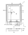
図1は、本発明の一実施例によるディスプレイ装置1を概略的に示す斜視図である。
Figure 1 is a perspective view showing a schematic diagram of a
図1を参照すれば、ディスプレイ装置1は、イメージを具現する表示領域DAとイメージを具現しない非表示領域である周辺領域PAを含む。ディスプレイ装置1は、表示領域DAに配置された画素Pからの放出光を用いて外部にイメージを提供することができる。
Referring to FIG. 1, the
図1では、表示領域DAが方形であるディスプレイ装置1を図示しているが、本発明は、それに限定されない。表示領域DAの形状は、円形、楕円形、または三角形や五角形のような多角形であってもよい。また、図1のディスプレイ装置1は、フラット(flat)状の平板ディスプレイ装置を図示するが、ディスプレイ装置1は、フレキシブル、ベンダブル、ホルダブル、ローラブル(flexible、bendable、foldable、rollable)ディスプレイ装置など多様な形態に具現されるということは言うまでもない。ディスプレイ装置1がフレキシブル、ベンダブル、ホルダブルに具現される場合、表示領域DAの一部または全体がフレキシブル、ベンダブル、ホルダブルにも具現される。
Although FIG. 1 illustrates a
図示されていないが、ディスプレイ装置1は、ディスプレイパネル10(図2)の一側に位置したコンポーネント(component)(図示せず)を含んでもよい。コンポーネントは、光や音響を用いる電子要素であってもよい。例えば、電子要素は、赤外線センサーのように光を受光して用いるセンサー、光を受光してイメージを撮像するカメラ、光や音響を出力し、感知して距離を測定するか、指紋などを認識するセンサー、光を出力する小型ランプであるか、音を出力するスピーカなどであってもよい。
Although not shown, the
以下では、本発明の一実施例によるディスプレイ装置1として、有機発光ディスプレイ装置を例として説明するが、本発明のディスプレイ装置は、それに制限されない。他の実施例として、本発明のディスプレイ装置1は、無機発光ディスプレイ装置(Inorganic Light Emitting Displayまたは無機ELディスプレイ装置)であるか、量子点発光ディスプレイ装置(Quantumdot Light Emitting Display)のようなディスプレイ装置であってもよい。例えば、ディスプレイ装置1に備えられた表示要素の発光層は、有機物を含んだり、無機物を含んだり、量子点を含んだり、有機物と量子点を含んだり、無機物と量子点を含んだりもする。
Hereinafter, an organic light emitting display device will be described as an example of a
図2は、本発明の一実施例によるディスプレイパネル10を概略的に示す平面図である。
Figure 2 is a plan view that shows a schematic diagram of a
図2を参照すれば、ディスプレイ装置1は、基板100の表示領域DAに配置された画素Pを含む。画素Pは、有機発光ダイオードOLEDのような表示要素を含んでもよい。画素Pは、複数個備えられ、有機発光ダイオードOLEDを通じて、例えば、赤色、緑色、青色または白色の光を放出することができる。本実施例において、画素Pは、実質的に副画素を意味し、表示領域DAから画素Pは、少なくとも1つ以上グルーピング(grouping)されて一単位画素を構成することができる。
Referring to FIG. 2, the
表示領域DAは、薄膜封止層300を通じてカバー(cover)されて外気または、水分などから保護されうる。薄膜封止層300は、表示領域DAの全面に対応するように一体に備えられ、周辺領域PA上にも一部配置されうる。薄膜封止層300は、後述する第1スキャン駆動回路120、第2スキャン駆動回路130、データ駆動回路150、第1電源供給配線160及び第2電源供給配線170の一部または全部を覆うように備えられてもよい。有機発光ダイオードOLEDは、水分及び酸素など外部要因に脆弱な特性を有するところ、薄膜封止層300を通じて有機発光ダイオードOLEDを密封することで、ディスプレイパネル10の信頼性を向上させうる。ディスプレイパネル10が後述する封止基板の代わりに、薄膜封止層300を備える場合、ディスプレイパネル10の厚さを減少させると共に、可撓性(flexibility)を向上させうる。
The display area DA may be covered by the thin
選択的実施例において、薄膜封止層300の代わりに、基板100上部に封止基板(図示せず)が備えられてもよい。封止基板は、基板100上に形成された構成要素を挟んで基板100と対向して配置されうる。封止基板は、周辺領域PA上に位置したシーラント(sealant)(図示せず)を通じて基板100と密着し、表示領域DAを外部から密封して有機発光ダイオードOLEDのような表示要素が外気及び水分に露出されることを防止することができる。
In an alternative embodiment, instead of the thin
画素Pは、周辺領域PAに配置された外郭回路と電気的に接続される。周辺領域Paには、第1スキャン駆動回路120、第2スキャン駆動回路130、端子140、データ駆動回路150、第1電源供給配線160、及び第2電源供給配線170が配置されうる。
The pixel P is electrically connected to an outer circuit arranged in the peripheral region PA. In the peripheral region Pa, a first scan driving circuit 120, a second
第1スキャン駆動回路120は、スキャンラインSLを通じて各画素SPにスキャン信号を提供することができる。第1スキャン駆動回路120の一側には、発光制御駆動回路122が位置する。発光制御駆動回路122は、発光制御線ELを通じて各画素に発光制御信号を提供することができる。第2スキャン駆動回路130は、表示領域DAを挟んで第1スキャン駆動回路120と並んで配置されてもよい。表示領域DAに配置された画素Pのうち、一部は、第1スキャン駆動回路120と電気的に接続され、残りは、第2スキャン駆動回路130に接続される。他の実施例において、第2スキャン駆動回路130は省略されてもよい。
The first scan driving circuit 120 can provide a scan signal to each pixel SP through a scan line SL. The emission control driving circuit 122 is located on one side of the first scan driving circuit 120. The emission control driving circuit 122 can provide an emission control signal to each pixel through an emission control line EL. The second
端子140は、基板100の一側に配置されてもよい。端子140は、絶縁層によって覆われず、露出されて印刷回路基板PCBと電気的に接続される。印刷回路基板PCBの端子PCB-Pは、ディスプレイパネル10の端子140と電気的に接続される。印刷回路基板PCBは、制御部(図示せず)の信号または電源をディスプレイパネル10に伝達する。
The terminal 140 may be disposed on one side of the
制御部で生成された制御信号は、印刷回路基板PCBを通じて第1及び第2スキャン駆動回路120、130にそれぞれ伝達されうる。制御部は、第1及び第2電源伝達161、171を通じて第1及び第2電源供給配線160、170にそれぞれ第1及び第2電源電圧ELVDD、ELVSSを提供することができる。第1電源電圧ELVDDは、第1電源供給配線160と接続された駆動電圧ラインPLを通じて各画素Pの画素回路に提供され、第2電源電圧ELVSSは、第2電源供給配線170と接続された各画素Pの対向電極に提供されうる。
The control signal generated by the control unit can be transmitted to the first and second
データ駆動回路150は、データラインDLに電気的に接続される。データ駆動回路150のデータ信号は、端子140に接続された信号送信配線151及び信号送信配線151と接続されたデータラインDLを通じて各画素Pに提供されうる。図2は、データ駆動回路150が印刷回路基板PCBに配置されたところを図示するが、他の実施例において、データ駆動回路150は、基板100上に配置されてもよい。例えば、データ駆動回路150は、端子140と第1電源供給配線160との間に配置されてもよい。
The
第1電源供給配線160は、表示領域DAを挟んでx方向に沿って平行に延びた第1サブ配線162及び第2サブ配線163を含んでもよい。第2電源供給配線170は、一側が開放されたループ状であり、表示領域DAを部分的に取り囲んでいる。
The first
図3A及び図3Bは、本発明の一実施例によるディスプレイ装置に含まれる画素の等価回路図である。 Figures 3A and 3B are equivalent circuit diagrams of a pixel included in a display device according to one embodiment of the present invention.
図3Aを参照すれば、各画素Pは、駆動電圧ラインPL、スキャンラインSL及びデータラインDLに接続された画素回路PC及び画素回路PCに接続された有機発光ダイオードOLEDを含む。 Referring to FIG. 3A, each pixel P includes a pixel circuit PC connected to a driving voltage line PL, a scan line SL, and a data line DL, and an organic light emitting diode OLED connected to the pixel circuit PC.
画素回路PCは、駆動薄膜トランジスタTd、スイッチング薄膜トランジスタTs及びストレージキャパシタCstを含む。スイッチング薄膜トランジスタTsは、スキャンラインSL及びデータラインDLに接続され、スキャンラインSLを介して入力されるスキャン信号SnによってデータラインDLを介して入力されたデータ信号Dmを駆動薄膜トランジスタTdに伝達する。 The pixel circuit PC includes a driving thin film transistor Td, a switching thin film transistor Ts, and a storage capacitor Cst. The switching thin film transistor Ts is connected to a scan line SL and a data line DL, and transmits a data signal Dm input via the data line DL to the driving thin film transistor Td in response to a scan signal Sn input via the scan line SL.
ストレージキャパシタCstは、スイッチング薄膜トランジスタTs及び駆動電圧ラインPLに接続され、スイッチング薄膜トランジスタTsから伝達された電圧と駆動電圧ラインPLに供給される駆動電圧、すなわち、第1電源電圧ELVDDの差に該当する電圧を保存する。 The storage capacitor Cst is connected to the switching thin film transistor Ts and the driving voltage line PL, and stores a voltage corresponding to the difference between the voltage transmitted from the switching thin film transistor Ts and the driving voltage supplied to the driving voltage line PL, i.e., the first power supply voltage ELVDD.
駆動薄膜トランジスタTdは、駆動電圧ラインPLとストレージキャパシタCstに接続され、ストレージキャパシタCstに保存された電圧値に対応して駆動電圧ラインPLから有機発光ダイオードOLEDを流れる駆動電流を制御することができる。有機発光ダイオードOLEDは、駆動電流によって所定の輝度を有する光を放出することができる。 The driving thin film transistor Td is connected to the driving voltage line PL and the storage capacitor Cst, and can control the driving current flowing from the driving voltage line PL to the organic light emitting diode OLED in response to the voltage value stored in the storage capacitor Cst. The organic light emitting diode OLED can emit light having a predetermined brightness according to the driving current.
図3Aでは、画素回路PCが2個の薄膜トランジスタ及び1個のストレージキャパシタを含む場合を説明したが、本発明は、それに限定されない。他の実施例において、画素回路PCは、図3Bのように7個の薄膜トランジスタ及び1個のストレージキャパシタを含んでもよい。他の実施例において、画素回路PCは、2個以上のストレージキャパシタを含んでもよい。 In FIG. 3A, the pixel circuit PC includes two thin film transistors and one storage capacitor, but the present invention is not limited thereto. In another embodiment, the pixel circuit PC may include seven thin film transistors and one storage capacitor as in FIG. 3B. In another embodiment, the pixel circuit PC may include two or more storage capacitors.
図3Bを参照すれば、画素Pは、画素回路PC及び画素回路PCに接続された有機発光ダイオードOLEDを含む。画素回路PCは、複数の薄膜トランジスタT1~T7及びストレージキャパシタCstを含んでもよい。薄膜トランジスタT1~T7及びストレージキャパシタは、信号ラインSL、SL-1、EL、DL、初期化電圧ラインVL及び駆動電圧ラインPLに接続されうる。 Referring to FIG. 3B, a pixel P includes a pixel circuit PC and an organic light emitting diode OLED connected to the pixel circuit PC. The pixel circuit PC may include a plurality of thin film transistors T1 to T7 and a storage capacitor Cst. The thin film transistors T1 to T7 and the storage capacitor may be connected to signal lines SL, SL-1, EL, DL, an initialization voltage line VL, and a driving voltage line PL.
図3Bでは、各画素Pが信号ラインSL、SL-1、EL、DL、初期化電圧ラインVL及び駆動電圧ラインPLに接続されているところを図示しているが、本発明は、それに限定されない。他の実施例として、信号ラインSL、SL-1、EL、DLのうち、少なくともいずれか1本、初期化電圧ラインVLと駆動電圧ラインPLなどは、隣接する画素で共有されうる。 In FIG. 3B, each pixel P is shown connected to signal lines SL, SL-1, EL, DL, an initialization voltage line VL, and a driving voltage line PL, but the present invention is not limited thereto. In another embodiment, at least one of the signal lines SL, SL-1, EL, DL, the initialization voltage line VL, and the driving voltage line PL may be shared by adjacent pixels.
複数の薄膜トランジスタT1~T7は、駆動薄膜トランジスタ(driving TFT, T1)、スイッチング薄膜トランジスタ(switching TFT, T2)、補償薄膜トランジスタT3、第1初期化薄膜トランジスタT4、動作制御薄膜トランジスタT5、発光制御薄膜トランジスタT6及び第2初期化薄膜トランジスタT7を含んでもよい。 The plurality of thin film transistors T1 to T7 may include a driving thin film transistor (T1), a switching thin film transistor (T2), a compensation thin film transistor T3, a first initialization thin film transistor T4, an operation control thin film transistor T5, a light emission control thin film transistor T6, and a second initialization thin film transistor T7.
信号ラインは、スキャン信号Snを駆動薄膜トランジスタT1と補償薄膜トランジスタT3に伝達するスキャンラインSL、第1初期化薄膜トランジスタT4と第2初期化薄膜トランジスタT7に以前スキャン信号Sn-1を伝達する以前スキャンラインSL-1、動作制御薄膜トランジスタT5及び発光制御薄膜トランジスタT6に発光制御信号Enを伝達する発光制御ラインEL、スキャンラインSLと交差し、データ信号Dmを伝達するデータラインDLを含む。 The signal lines include a scan line SL that transmits a scan signal Sn to the driving thin film transistor T1 and the compensation thin film transistor T3, a previous scan line SL-1 that transmits a previous scan signal Sn-1 to the first initialization thin film transistor T4 and the second initialization thin film transistor T7, an emission control line EL that transmits an emission control signal En to the operation control thin film transistor T5 and the emission control thin film transistor T6, and a data line DL that crosses the scan line SL and transmits a data signal Dm.
駆動電圧ラインPLは、駆動薄膜トランジスタT1に駆動電圧ELVDDを伝達し、初期化電圧ラインVLは、駆動薄膜トランジスタT1及び画素電極を初期化する初期化電圧Vintを伝達する。 The driving voltage line PL transmits the driving voltage ELVDD to the driving thin film transistor T1, and the initialization voltage line VL transmits the initialization voltage Vint that initializes the driving thin film transistor T1 and the pixel electrode.
駆動薄膜トランジスタT1の駆動ゲート電極G1は、ストレージキャパシタCstの第1ストレージ蓄電板Cst1に接続されている。駆動薄膜トランジスタT1の駆動ソース電極S1は、動作制御薄膜トランジスタT5を経て駆動電圧ラインPLに接続されている。駆動薄膜トランジスタT1の駆動ドレイン電極D1は、発光制御薄膜トランジスタT6を経て有機発光ダイオードOLEDの画素電極と電気的に接続されている。駆動薄膜トランジスタT1は、スイッチング薄膜トランジスタT2のスイッチング動作によってデータ信号Dmを伝達されて有機発光ダイオードOLEDに駆動電流IOLEDを供給する。 A driving gate electrode G1 of the driving thin film transistor T1 is connected to a first storage capacitor plate Cst1 of the storage capacitor Cst. A driving source electrode S1 of the driving thin film transistor T1 is connected to a driving voltage line PL via an operation control thin film transistor T5. A driving drain electrode D1 of the driving thin film transistor T1 is electrically connected to a pixel electrode of the organic light emitting diode OLED via an emission control thin film transistor T6. The driving thin film transistor T1 receives a data signal Dm through a switching operation of the switching thin film transistor T2 and supplies a driving current IOLED to the organic light emitting diode OLED.
スイッチング薄膜トランジスタT2のスイッチングゲート電極G2は、スキャンラインSLに接続されている。スイッチング薄膜トランジスタT2のスイッチングソース電極S2は、データラインDLに接続されている。スイッチング薄膜トランジスタT2のスイッチングドレイン電極D2は、駆動薄膜トランジスタT1の駆動ソース電極S1に接続されており、かつ動作制御薄膜トランジスタT5を経て下部駆動電圧ラインPLに接続されている。スイッチング薄膜トランジスタT2は、スキャンラインSLを介して伝達されたスキャン信号Snによってターンオンされ、データラインDLに伝達されたデータ信号Dmを駆動薄膜トランジスタT1の駆動ソース電極S1に伝達するスイッチング動作を行う。 The switching gate electrode G2 of the switching thin film transistor T2 is connected to the scan line SL. The switching source electrode S2 of the switching thin film transistor T2 is connected to the data line DL. The switching drain electrode D2 of the switching thin film transistor T2 is connected to the driving source electrode S1 of the driving thin film transistor T1, and is also connected to the lower driving voltage line PL via the operation control thin film transistor T5. The switching thin film transistor T2 is turned on by the scan signal Sn transmitted through the scan line SL, and performs a switching operation of transmitting the data signal Dm transmitted to the data line DL to the driving source electrode S1 of the driving thin film transistor T1.
補償薄膜トランジスタT3の補償ゲート電極G3は、スキャンラインSLに接続されている。補償薄膜トランジスタT3の補償ソース電極S3は、駆動薄膜トランジスタT1の駆動ドレイン電極D1に接続されており、かつ発光制御薄膜トランジスタT6を経て有機発光ダイオードOLEDの画素電極と接続されている。補償薄膜トランジスタT3の補償ドレイン電極D3は、ストレージキャパシタCstの第1ストレージ蓄電板Cst1、第1初期化薄膜トランジスタT4の第1初期化ドレイン電極D4及び駆動薄膜トランジスタT1の駆動ゲート電極G1に接続されている。補償薄膜トランジスタT3は、スキャンラインSLを介して伝達されたスキャン信号Snによってターンオンされ、駆動薄膜トランジスタT1の駆動ゲート電極G1と駆動ドレイン電極D1とを電気的に接続して駆動薄膜トランジスタT1をダイオード接続(Diode connection)させる。 The compensation gate electrode G3 of the compensation thin film transistor T3 is connected to the scan line SL. The compensation source electrode S3 of the compensation thin film transistor T3 is connected to the driving drain electrode D1 of the driving thin film transistor T1, and is connected to the pixel electrode of the organic light emitting diode OLED via the light emitting control thin film transistor T6. The compensation drain electrode D3 of the compensation thin film transistor T3 is connected to the first storage capacitor plate Cst1 of the storage capacitor Cst, the first initialization drain electrode D4 of the first initialization thin film transistor T4, and the driving gate electrode G1 of the driving thin film transistor T1. The compensation thin film transistor T3 is turned on by the scan signal Sn transmitted via the scan line SL, and electrically connects the driving gate electrode G1 and the driving drain electrode D1 of the driving thin film transistor T1 to make the driving thin film transistor T1 diode connected.
第1初期化薄膜トランジスタT4の第1初期化ゲート電極G4は、以前スキャンラインSL-1に接続されている。第1初期化薄膜トランジスタT4の第1初期化ソース電極S4は、第2初期化薄膜トランジスタT7の第2初期化ドレイン電極D7と初期化電圧ラインVLに接続されている。第1初期化薄膜トランジスタT4の第1初期化ドレイン電極D4は、ストレージキャパシタCstの第1ストレージ蓄電板Cst1、補償薄膜トランジスタT3の補償ドレイン電極D3及び駆動薄膜トランジスタT1の駆動ゲート電極G1に接続されている。第1初期化薄膜トランジスタT4は、以前スキャンラインSL-1を介して伝達された以前スキャン信号Sn-1によってターンオンされ、初期化電圧Vintを駆動薄膜トランジスタT1の駆動ゲート電極G1に伝達して駆動薄膜トランジスタT1の駆動ゲート電極G1の電圧を初期化させる初期化動作を行う。 The first initialization gate electrode G4 of the first initialization thin film transistor T4 is connected to the previous scan line SL-1. The first initialization source electrode S4 of the first initialization thin film transistor T4 is connected to the second initialization drain electrode D7 of the second initialization thin film transistor T7 and the initialization voltage line VL. The first initialization drain electrode D4 of the first initialization thin film transistor T4 is connected to the first storage capacitor plate Cst1 of the storage capacitor Cst, the compensation drain electrode D3 of the compensation thin film transistor T3, and the driving gate electrode G1 of the driving thin film transistor T1. The first initialization thin film transistor T4 is turned on by the previous scan signal Sn-1 transmitted through the previous scan line SL-1, and transmits the initialization voltage Vint to the driving gate electrode G1 of the driving thin film transistor T1 to perform an initialization operation to initialize the voltage of the driving gate electrode G1 of the driving thin film transistor T1.
動作制御薄膜トランジスタT5の動作制御ゲート電極G5は、発光制御ラインELに接続されている。動作制御薄膜トランジスタT5の動作制御ソース電極S5は、下部駆動電圧ラインPLと接続されている。動作制御薄膜トランジスタT5の動作制御ドレイン電極D5は、駆動薄膜トランジスタT1の駆動ソース電極S1及びスイッチング薄膜トランジスタT2のスイッチングドレイン電極D2と接続されている。 The operation control gate electrode G5 of the operation control thin film transistor T5 is connected to the light emission control line EL. The operation control source electrode S5 of the operation control thin film transistor T5 is connected to the lower drive voltage line PL. The operation control drain electrode D5 of the operation control thin film transistor T5 is connected to the drive source electrode S1 of the drive thin film transistor T1 and the switching drain electrode D2 of the switching thin film transistor T2.
発光制御薄膜トランジスタT6の発光制御ゲート電極G6は、発光制御ラインELに接続されている。発光制御薄膜トランジスタT6の発光制御ソース電極S6は、駆動薄膜トランジスタT1の駆動ドレイン電極D1及び補償薄膜トランジスタT3の補償ソース電極S3に接続されている。発光制御薄膜トランジスタT6の発光制御ドレイン電極D6は、第2初期化薄膜トランジスタT7の第2初期化ソース電極S7及び有機発光ダイオードOLEDの画素電極に電気的に接続されている。 The emission control gate electrode G6 of the emission control thin film transistor T6 is connected to the emission control line EL. The emission control source electrode S6 of the emission control thin film transistor T6 is connected to the driving drain electrode D1 of the driving thin film transistor T1 and the compensation source electrode S3 of the compensation thin film transistor T3. The emission control drain electrode D6 of the emission control thin film transistor T6 is electrically connected to the second initialization source electrode S7 of the second initialization thin film transistor T7 and the pixel electrode of the organic light emitting diode OLED.
動作制御薄膜トランジスタT5及び発光制御薄膜トランジスタT6は、発光制御ラインELを介して伝達された発光制御信号Enによって同時にターンオンされ、駆動電圧ELVDDが有機発光ダイオードOLEDに伝達され、有機発光ダイオードOLEDに駆動電流IOLEDが流れるようにする。 The operation control thin film transistor T5 and the emission control thin film transistor T6 are simultaneously turned on by an emission control signal En transmitted through an emission control line EL, so that the driving voltage ELVDD is transmitted to the organic light emitting diode OLED and a driving current IOLED flows through the organic light emitting diode OLED .
第2初期化薄膜トランジスタT7の第2初期化ゲート電極G7は、以前スキャンラインSL-1に接続されている。第2初期化薄膜トランジスタT7の第2初期化ソース電極S7は、発光制御薄膜トランジスタT6の発光制御ドレイン電極D6及び有機発光ダイオードOLEDの画素電極に接続されている。第2初期化薄膜トランジスタT7の第2初期化ドレイン電極D7は、第1初期化薄膜トランジスタT4の第1初期化ソース電極S4及び初期化電圧ラインVLに接続されている。第2初期化薄膜トランジスタT7は、以前スキャンラインSL-1を介して伝達された以前スキャン信号Sn-1によってターンオンされ、有機発光ダイオードOLEDの画素電極を初期化させる。 The second initialization gate electrode G7 of the second initialization thin film transistor T7 is connected to the previous scan line SL-1. The second initialization source electrode S7 of the second initialization thin film transistor T7 is connected to the emission control drain electrode D6 of the emission control thin film transistor T6 and the pixel electrode of the organic light emitting diode OLED. The second initialization drain electrode D7 of the second initialization thin film transistor T7 is connected to the first initialization source electrode S4 of the first initialization thin film transistor T4 and the initialization voltage line VL. The second initialization thin film transistor T7 is turned on by the previous scan signal Sn-1 transmitted via the previous scan line SL-1 to initialize the pixel electrode of the organic light emitting diode OLED.
図3Bでは、初期化薄膜トランジスタT4と第2初期化薄膜トランジスタT7とが以前スキャンラインSL-1に接続された場合を図示しているが、本発明は、それに限定されない。他の実施例として、初期化薄膜トランジスタT4は、以前スキャンラインSL-1に接続されて以前スキャン信号Sn-1によって駆動し、第2初期化薄膜トランジスタT7は、別途の信号ライン(例えば、以後スキャンライン)に接続され、前記信号ラインに伝達される信号によって駆動されうる。 In FIG. 3B, the initialization thin film transistor T4 and the second initialization thin film transistor T7 are shown connected to the previous scan line SL-1, but the present invention is not limited thereto. In another embodiment, the initialization thin film transistor T4 can be connected to the previous scan line SL-1 and driven by the previous scan signal Sn-1, and the second initialization thin film transistor T7 can be connected to a separate signal line (e.g., the future scan line) and driven by a signal transmitted to the signal line.
ストレージキャパシタCstの第2ストレージ蓄電板Cst2は、駆動電圧ラインPLに接続されている。有機発光ダイオードOLEDの対向電極は、共通電圧ELVSSに接続されている。これにより、有機発光ダイオードOLEDは、駆動薄膜トランジスタT1から駆動電流IOLEDを伝達されて発光することで、画像を表示することができる。 A second storage capacitor Cst2 of the storage capacitor Cst is connected to the driving voltage line PL. A counter electrode of the organic light emitting diode OLED is connected to a common voltage ELVSS. Thus, the organic light emitting diode OLED receives a driving current IOLED from the driving thin film transistor T1 to emit light and display an image.
図3Bでは、補償薄膜トランジスタT3と初期化薄膜トランジスタT4がデュアルゲート電極を有すると図示しているが、補償薄膜トランジスタT3と初期化薄膜トランジスタT4は、1つのゲート電極を有することができる。 In FIG. 3B, the compensation thin film transistor T3 and the initialization thin film transistor T4 are illustrated as having dual gate electrodes, but the compensation thin film transistor T3 and the initialization thin film transistor T4 may have a single gate electrode.
図4A及び図4Bは、本発明の一実施例によるディスプレイ装置の一画素の概略的な断面図である。 Figures 4A and 4B are schematic cross-sectional views of one pixel of a display device according to one embodiment of the present invention.
まず、図4Aを参照すれば、表示領域DAに位置した画素Pは、画素回路PCを含み、画素回路PCは、薄膜トランジスタTFT及びストレージキャパシタCstを含む。図4Aの薄膜トランジスタTFTは、図3Aの薄膜トランジスタTd、Tsのうちの1つであってもよく、例えば、駆動薄膜トランジスタTdであってもよい。 First, referring to FIG. 4A, a pixel P located in a display area DA includes a pixel circuit PC, which includes a thin film transistor TFT and a storage capacitor Cst. The thin film transistor TFT in FIG. 4A may be one of the thin film transistors Td and Ts in FIG. 3A, for example, a driving thin film transistor Td.
画素回路層110は、基板100上に順次に位置するバッファ層101、ゲート絶縁層103、第1層間絶縁層107及び平坦化層109を含んでもよい。
The
バッファ層101は、不純物の浸透を防止するため、基板100上に配置され、ゲート絶縁層103は、薄膜トランジスタTFTの半導体層211とゲート電極213との間に介在されうる。第1層間絶縁層107は、薄膜トランジスタTFTのゲート電極213とソース電極215s及びドレイン電極215dとの間に介在される共に、ストレージキャパシタCstの下部電極217と上部電極219との間に介在されて誘電体として機能しうる。
The
バッファ層101、ゲート絶縁層103、第1層間絶縁層107はいずれも絶縁性無機物によって形成される。例えば、バッファ層101、ゲート絶縁層103、及び第1層間絶縁層107は、それぞれシリコン窒化物、シリコン酸化物、及び/またはシリコン酸窒化物によって形成されうる。
The
図4Aでは、画素回路PCの薄膜トランジスタTFTがトップゲートタイプである場合を説明したが、本発明は、それに制限されない。他の実施例において、薄膜トランジスタTFTは、ボトムゲートタイプであってもよい。 In FIG. 4A, the thin film transistor TFT of the pixel circuit PC is described as being of a top gate type, but the present invention is not limited thereto. In other embodiments, the thin film transistor TFT may be of a bottom gate type.
また、図4では、ストレージキャパシタCstの下部電極217と上部電極219がそれぞれゲート電極213とソース電極215s及びドレイン電極215dと同一物質を含むように同一層に位置する場合を説明したが、本発明は、それに制限されず、多様に変更可能である。
In addition, in FIG. 4, the
有機発光ダイオードOLEDは、コンタクトホールを有する平坦化層109を挟んで画素回路PCと電気的に接続された画素電極210、画素電極210と対向する対向電極230及びそれらの間に介在される中間層220を含む。一実施例において、平坦化層109は、絶縁性有機物によっても形成される。
The organic light-emitting diode OLED includes a
画素電極210は、画素定義膜240に備えられた開口OPを通じて露出され、画素電極210の縁部は、絶縁性有機物によって形成された画素定義膜240によってカバーされうる。一実施例として、画素電極210は、銀(Ag)、マグネシウム(Mg)、アルミニウム(Al)、白金(Pt)、パラジウム(Pd)、金(Au)、ニッケル(Ni)、ネオジム(Nd)、イリジウム(Ir)、クロム(Cr)またはそれらの化合物を含んでもよい。
The
対向電極230は、一体に形成されて表示領域DAを全体としてカバーすることができる。一実施例として、対向電極230は、銀(Ag)とマグネシウム(Mg)とを含む薄膜金属層、または酸化インジウムスズ(ITO; indium tin oxide)、酸化インジウム亜鉛(IZO; indium zinc oxide)、酸化亜鉛(ZnO; zinc oxide)、酸化インジウム(In2O3 indium oxide)、酸化インジウムガリウム(IGO; indium gallium oxide)、またはアルミニウム酸化亜鉛(AZO; aluminum zinc oxide)のような透光性導電層(TCO、transparent conductive oxide)であってもよい。
The
中間層220は、赤色、緑色及び青色の光を放出する蛍光またはリン光物質を含む有機物によって形成され、表示領域DAのうち、画素Pに対応してパターニングされうる。
The
本実施例において、中間層220は、発光層223を含んでもよい。発光層223の上/下部には、発光層223を挟んで発光層223と画素電極210との間に介在される第1機能層221及び中間層220と対向電極230との間に介在される第2機能層222のうち、少なくともいずれか1つの機能層を含んでもよい。第1機能層221と第2機能層222は、画素電極210上にパターニングされて形成される発光層223とは異なって、表示領域DAの全面にわたって形成される共通層であってもよい。
In this embodiment, the
第1機能層221は、例えば、正孔注入層(HIL: Hole Injection Layer)及び正孔輸送層(HTL: Hole Transport Layer)のうち、少なくともいずれか1つを含んでもよい。正孔注入層は、アノードから正孔を容易に放出させ、正孔輸送層は、正孔注入層の正孔を発光層まで伝達させる。第2機能層222は、電子輸送層(ETL: Electron Transport Layer)及び電子注入層(EIL: Electron Injection Layer)のうち、少なくともいずれか1つを含んでもよい。電子注入層は、カソードから電子を容易に放出させ、電子輸送層は、電子注入層の電子を発光層まで伝達させる。
The first
有機発光ダイオードOLED上には、薄膜封止層300が配置される。図4Aでは、薄膜封止層300が表示領域DA上に位置したところを図示しているが、薄膜封止層300は、図2のように周辺領域PA上にも一部配置されうる。
A thin-
薄膜封止層300は、第1及び第2無機封止層310、330と有機封止層320を含む。例えば、薄膜封止層300は、第1無機封止層310、有機封止層320、及び第2無機封止層330が順次に積層されて形成されうる。第1及び第2無機封止層310、330は、シリコン窒化物、アルミニウム窒化物、ジルコニウム窒化物、チタン窒化物、ハフニウム窒化物、タンタル窒化物、シリコン酸化物、アルミニウム酸化物、チタン酸化物、錫酸化物、セリウム酸化物、及びシリコン酸窒化物のうち、少なくともいずれか1つの物質を含んでもよい。第1及び第2無機封止層310、330は、例えば、化学気相蒸着(CVD)工程によっても形成される。
The thin
有機封止層320は、アクリル系樹脂、メタクリル系樹脂、ポリイソプレン、ビニル系樹脂、エポキシ系樹脂、ウレタン系樹脂、セルロース系樹脂及びペリレン系樹脂からなる群から選択された1つ以上の物質を含んでもよい。一実施例として、有機封止層320は、HMDSO(hexamethyldisiloxane)またはTEOS (tetraethly orthosilicate)のような物質を原料ガスとして使用した原子層蒸着(ALD: Atomic Layer Deposition)工程によって形成されうる。さらに他の実施例において、有機封止層320は、液状のモノマーを蒸着した後、熱や紫外線のような光を用いて硬化させることで形成されうる。
The
本実施例では、薄膜封止層300が2つの第1及び第2無機封止層310、330及び1つの有機封止層320を備える場合を説明したが、無機封止層と有機封止層の積層順序及び個数は、その限りではない。
In this embodiment, the thin
一方、図4Bの画素回路PCは、図4Aの画素回路PC構造とは相違する。その他の構成は、図4Aと同一であるところ、以下では、画素回路構造の相違点を中心に説明する。 On the other hand, the pixel circuit PC in FIG. 4B has a different structure from the pixel circuit PC in FIG. 4A. The rest of the configuration is the same as in FIG. 4A, so the following description will focus on the differences in the pixel circuit structure.
図4Bを参照すれば、表示領域DAに位置した画素P’は、画素回路PC’を含み、画素回路PC’は、薄膜トランジスタTFT’及びストレージキャパシタCst’を含む。図4Bの薄膜トランジスタTFT’は、図3Bの薄膜トランジスタT1~T7のうち、1つであってもよく、例えば、駆動薄膜トランジスタT1であってもよい。 Referring to FIG. 4B, a pixel P' located in the display area DA includes a pixel circuit PC', which includes a thin film transistor TFT' and a storage capacitor Cst'. The thin film transistor TFT' in FIG. 4B may be one of the thin film transistors T1 to T7 in FIG. 3B, for example, the driving thin film transistor T1.
画素回路PC’は、薄膜トランジスタTFT’及びストレージキャパシタCst’を含む。画素回路層110’は、基板100上に順次に位置するバッファ層101’、ゲート絶縁層103’、誘電体絶縁層105’、第2層間絶縁層107’、及び平坦化層109’を含んでもよい。
The pixel circuit PC' includes a thin film transistor TFT' and a storage capacitor Cst'. The pixel circuit layer 110' may include a buffer layer 101', a gate insulating layer 103', a dielectric insulating layer 105', a second interlayer insulating layer 107', and a planarization layer 109', which are sequentially disposed on the
バッファ層101’は、不純物の浸透を防止するために、基板100上に配置される。ゲート絶縁層103’は、薄膜トランジスタTFT’の半導体層211’とゲート電極213’との間に介在される。誘電体絶縁層105’は、ストレージキャパシタCst’の下部電極217’と上部電極219’との間に介在される。第2層間絶縁層107’は、薄膜トランジスタTFT’のゲート電極213’とソース電極215s’及びドレイン電極215d’との間に介在される。
The buffer layer 101' is disposed on the
バッファ層101’、ゲート絶縁層103’、誘電体絶縁層105’、層間絶縁層107’及び平坦化層109’はいずれも絶縁性無機物によって形成される。例えば、バッファ層101’、ゲート絶縁層103’、誘電体絶縁層105’、層間絶縁層107’、及び平坦化層109’は、それぞれシリコン窒化物、シリコン酸化物、及び/またはシリコン酸窒化物によっても形成される。 The buffer layer 101', the gate insulating layer 103', the dielectric insulating layer 105', the interlayer insulating layer 107', and the planarization layer 109' are all formed of insulating inorganic materials. For example, the buffer layer 101', the gate insulating layer 103', the dielectric insulating layer 105', the interlayer insulating layer 107', and the planarization layer 109' are each formed of silicon nitride, silicon oxide, and/or silicon oxynitride.
図4Bでは、薄膜トランジスタTFT’とストレージキャパシタCst’とが重畳するように配置され、薄膜トランジスタTFT’のゲート電極213’がストレージキャパシタCst’の下部電極217’である場合を図示しているが、本発明は、それに限定されるものではない。 FIG. 4B illustrates a case in which the thin film transistor TFT' and the storage capacitor Cst' are arranged to overlap each other and the gate electrode 213' of the thin film transistor TFT' is the lower electrode 217' of the storage capacitor Cst', but the present invention is not limited thereto.
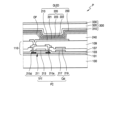
図5は、本発明の一実施例によるディスプレイ装置の表示領域の一部を概略的に示す平面図であり、図6は、図5のA1-A1’線に沿って見た概略的な断面図である。 Figure 5 is a plan view showing a schematic view of a portion of a display area of a display device according to one embodiment of the present invention, and Figure 6 is a schematic cross-sectional view taken along line A1-A1' in Figure 5.
図5を参照すれば、表示領域DAには、複数の画素P1、P2、P3が配置されうる。複数の画素P1、P2、P3は、第1画素P1、第2画素P2及び第3画素P3を含んでもよい。図5では、複数の画素P1、P2、P3がダイヤモンドペンタイル型(pentile type)として配置された構成を図示しているが、本発明が必ずしもそれに限定されるものではない。複数の画素P1、P2、P3は、例えば、ストライプ型(stripe type)または一般ペンタイル型によっても配置される。 Referring to FIG. 5, a plurality of pixels P1, P2, and P3 may be arranged in the display area DA. The plurality of pixels P1, P2, and P3 may include a first pixel P1, a second pixel P2, and a third pixel P3. Although FIG. 5 illustrates a configuration in which the plurality of pixels P1, P2, and P3 are arranged in a diamond pentile type, the present invention is not necessarily limited thereto. The plurality of pixels P1, P2, and P3 may also be arranged in, for example, a stripe type or a general pentile type.
第1画素P1、第2画素P2、及び第3画素P3は、それぞれ複数個備えられ、互いに異なる色を発光することができる。一実施例において、第1画素P1は、赤色光を発光し、第2画素P2は、緑光を発光し、第3画素P3は、青色光を発光することができる。一実施例において、赤色光を発光する第1画素P1の発光領域及び青色光を発光する第3画素P3の発光領域は、緑光を発光する第2画素P2の発光領域よりも大きくなる。 The first pixel P1, the second pixel P2, and the third pixel P3 are each provided in multiple numbers, and can emit light of different colors. In one embodiment, the first pixel P1 can emit red light, the second pixel P2 can emit green light, and the third pixel P3 can emit blue light. In one embodiment, the light-emitting area of the first pixel P1 that emits red light and the light-emitting area of the third pixel P3 that emits blue light are larger than the light-emitting area of the second pixel P2 that emits green light.
図6を参照すれば、第1画素P1、第2画素P2、及び第3画素P3のそれぞれは、基板100上に配置された画素回路PCに接続され、それぞれが第1ないし第3画素電極210R、210G、210Bを含んでもよい。第1ないし第3画素電極210R、210G、210B上には、それぞれ第1ないし第3中間層220R、220G、220Bが配置されうる。詳細には、第1ないし第3画素電極210R、210G、210B上には、共通層としての第1機能層221及び第2機能層222が配置され、第1機能層221及び第2機能層222の間には、それぞれ第1ないし第3発光層223R、223G、223Bが配置されうる。
Referring to FIG. 6, each of the first pixel P1, the second pixel P2, and the third pixel P3 may be connected to a pixel circuit PC arranged on the
本実施例において、複数の第1画素P1と複数の第2画素P2は、x、y軸と交差する斜線方向である第1方向ax1に沿って交互に配置されうる。また、複数の第3画素P3と複数の第2画素P2は、x、y軸と交差する斜線方向である第2方向ax2に沿って交互に配置されうる。第1方向ax1と第2方向ax2は、互いに交差する方向に、例えば互いに直交する。 In this embodiment, the multiple first pixels P1 and the multiple second pixels P2 can be arranged alternately along a first direction ax1, which is a diagonal direction intersecting the x and y axes. Also, the multiple third pixels P3 and the multiple second pixels P2 can be arranged alternately along a second direction ax2, which is a diagonal direction intersecting the x and y axes. The first direction ax1 and the second direction ax2 are directions that intersect with each other, for example, are perpendicular to each other.
このような画素配置構造を有する任意の4個の画素は、菱形に配置されてもよい。すなわち、最隣接の1個の第1画素P1、2個の第2画素P2、及び1個の第3画素P3を接続した仮想の線は、菱形であってもよい。したがって、第1方向ax1、または第2方向ax2に沿って配置された画素間の間隔(例、d1)は、第3方向ax3(すなわち、x方向)、または第4方向ax4(すなわち、y方向)に沿って配置された画素間の間隔(例、d1’)よりも狭く配置される。さらに、表示領域DAが高解像度化されることにより、画素間の間隔は、徐々に狭くなる。 Any four pixels having such a pixel arrangement structure may be arranged in a diamond shape. That is, a virtual line connecting the nearest first pixel P1, two nearest second pixels P2, and one nearest third pixel P3 may be diamond shaped. Therefore, the distance (e.g., d1) between pixels arranged along the first direction ax1 or the second direction ax2 is narrower than the distance (e.g., d1') between pixels arranged along the third direction ax3 (i.e., the x direction) or the fourth direction ax4 (i.e., the y direction). Furthermore, as the resolution of the display area DA is increased, the distance between pixels gradually becomes narrower.
その場合、相対的に画素間の最短距離が近く配置される第1画素P1と第2画素P2、第2画素P2と第3画素P3との間に漏れ電流が発生し、これにより、画素間の混色が発生する問題点があり得る。漏れ電流は、複数の画素P1、P2、P3に共通層として配置される有機物層、すなわち、第1機能層221及び/または第2機能層222を通じて隣接画素に伝達されるので、第1機能層221及び/または第2機能層222に沿って伝達される電流経路を増加させることが要求される。
In this case, leakage current occurs between the first pixel P1 and the second pixel P2, and between the second pixel P2 and the third pixel P3, which are arranged relatively close to each other, and this can cause a problem of color mixing between the pixels. Since the leakage current is transmitted to adjacent pixels through the organic layer arranged as a common layer for multiple pixels P1, P2, and P3, i.e., the first
これにより、本実施例では、図5及び図6に図示されたように、第1画素P1と第2画素P2との間に第1ダム部DM1を配置し、第2画素P2と第3画素P3との間に第2ダム部DM2を配置する。これを通じて、第1画素P1と第2画素P2との間、第2画素P2と第3画素P3との水平距離、すなわち、有機物層の経路を増加させることで、漏れ電流を最小化して、画素間の混色の発生を防止することができる。 In this embodiment, as shown in FIG. 5 and FIG. 6, a first dam portion DM1 is disposed between the first pixel P1 and the second pixel P2, and a second dam portion DM2 is disposed between the second pixel P2 and the third pixel P3. This increases the horizontal distance between the first pixel P1 and the second pixel P2 and between the second pixel P2 and the third pixel P3, i.e., the path of the organic layer, thereby minimizing leakage current and preventing color mixing between pixels.
図6を参照すれば、例えば、第1画素P1と第2画素P2との間に第1ダム部DM1を配置することで、第1ダム部DM1がない場合に比べて、おおよそ第1ダム部DM1の高さhの2倍ほどの水平距離、すなわち、有機物層の経路を増加させうる。そのような有機物層の経路は、後述する図9のように第1及び第2ダム部DM1、DM2のそれぞれが第1サブダムSDM1及び第2サブダムSDM2を備える場合、おおよそ第1ダム部DM1の高さhの4倍ほど有機物層の経路を増加させうる。また、後述する図10のように第1サブダムSDM1と第2サブダムSDM2との間にバレーVを形成する場合、図9の実施例に加えて、最小バレーVの深さh2の2倍ほど有機物層の経路をさらに増加させうる。一方、後述する図13及び図14のように、第1及び第2ダム部DM1、DM2が逆テーパ状を有する場合、断面が順テーパ状を有する図6または図9の実施例に比べて、有機物層の経路を小幅ながらにさらに増加させうる。 6, for example, by disposing the first dam part DM1 between the first pixel P1 and the second pixel P2, the horizontal distance, i.e., the path of the organic material layer, can be increased by approximately twice the height h of the first dam part DM1 compared to the case where the first dam part DM1 is not present. When the first and second dam parts DM1 and DM2 each have a first sub-dam SDM1 and a second sub-dam SDM2 as shown in FIG. 9 described below, the path of the organic material layer can be increased by approximately four times the height h of the first dam part DM1. Also, when a valley V is formed between the first sub-dam SDM1 and the second sub-dam SDM2 as shown in FIG. 10 described below, in addition to the embodiment of FIG. 9, the path of the organic material layer can be further increased by approximately twice the depth h2 of the minimum valley V. On the other hand, when the first and second dam portions DM1 and DM2 have an inverse tapered shape as shown in FIG. 13 and FIG. 14 described below, the path of the organic layer can be further increased, albeit slightly, compared to the embodiment of FIG. 6 or FIG. 9, in which the cross section has a forward tapered shape.
また、図5を参照すれば、図5のような平面上において、第1ダム部DM1及び第2ダム部DM2のそれぞれは、ほぼ多角形を有することができる。一実施例において、図5では、第1ダム部DM1及び第2ダム部DM2がそれぞれ方形に備えられたことを図示している。他の実施例において、第1ダム部DM1及び第2ダム部DM2のエッジは、面取りされた形状にも備えられる。そのような面取り形状は、工程的側面で示されるものであるが、第1ダム部DM1及び第2ダム部DM2のエッジは、必ずしも面取り形状ではない。 Referring further to FIG. 5, in a plane as shown in FIG. 5, each of the first dam portion DM1 and the second dam portion DM2 may have an approximately polygonal shape. In one embodiment, FIG. 5 illustrates that the first dam portion DM1 and the second dam portion DM2 are each provided in a square shape. In another embodiment, the edges of the first dam portion DM1 and the second dam portion DM2 may also be provided in a chamfered shape. Although such a chamfered shape is indicated from a process aspect, the edges of the first dam portion DM1 and the second dam portion DM2 are not necessarily chamfered shapes.
第1ダム部DM1及び第2ダム部DM2は、それぞれ長軸方向に第1幅W1を有し、短軸方向に第2幅w2を有することができる。図5において、第1ダム部DM1の長軸方向は、第1方向ax1を意味し、短軸方向は、第2方向ax2を意味することができる。また、第2ダム部DM2の長軸方向は、第2方向ax2を意味し、短軸方向は、第1方向ax1を意味することができる。 The first dam part DM1 and the second dam part DM2 may each have a first width W1 in the long axis direction and a second width w2 in the short axis direction. In FIG. 5, the long axis direction of the first dam part DM1 may refer to the first direction ax1, and the short axis direction may refer to the second direction ax2. Furthermore, the long axis direction of the second dam part DM2 may refer to the second direction ax2, and the short axis direction may refer to the first direction ax1.
一実施例において、第1ダム部DM1及び第2ダム部DM2の第1幅W1は、8μm以上12μm以下であり、第2幅w2は、4μm以上8μm以下であってもよく、望ましくは、第1幅W1は、10μm以上11μm以下であってもよく、第2幅w2は、6μm以上7μm以下であってもよい。図6を参照すれば、第1ダム部DM1及び第2ダム部DM2のそれぞれの高さhは、2μm以上に形成されればよい。一実施例において、第1ダム部DM1及び第2ダム部DM2のそれぞれの高さhは、2μm以上3.5μm以下であってもよく、望ましくは、2.5μm以上3μm以下であってもよい。 In one embodiment, the first width W1 of the first dam portion DM1 and the second dam portion DM2 may be 8 μm or more and 12 μm or less, and the second width w2 may be 4 μm or more and 8 μm or less, and preferably, the first width W1 may be 10 μm or more and 11 μm or less, and the second width w2 may be 6 μm or more and 7 μm or less. Referring to FIG. 6, the height h of each of the first dam portion DM1 and the second dam portion DM2 may be formed to be 2 μm or more. In one embodiment, the height h of each of the first dam portion DM1 and the second dam portion DM2 may be 2 μm or more and 3.5 μm or less, and preferably, the height h of each of the first dam portion DM1 and the second dam portion DM2 may be 2 μm or more and 3.5 μm or less.
第1画素P1、第2画素P2、及び第1ダム部DM1は、第1方向ax1に沿って配置され、第2画素P2、第3画素P3、及び第2ダム部DM2は、第2方向ax2に沿って配置されうる。上述したように、平面上で、第1方向ax1に沿う第1画素P1と第2画素P2との最短距離d1は、第3方向ax3(すなわち、x方向)に沿う第1画素P1と第3画素P3との最短距離d1’よりも短い。同様に、平面上で、第2方向ax2に沿う第2画素P2と第3画素P3との最短距離d1は、第3方向ax3(すなわち、x方向)に沿う第1画素P1と第3画素P3との最短距離d1’よりも短い。一実施例において、第1画素P1と第2画素P2との最短距離d1と、第2画素P2と第3画素P3との最短距離d1は、同一であってもよい。 The first pixel P1, the second pixel P2, and the first dam portion DM1 may be arranged along the first direction ax1, and the second pixel P2, the third pixel P3, and the second dam portion DM2 may be arranged along the second direction ax2. As described above, on a plane, the shortest distance d1 between the first pixel P1 and the second pixel P2 along the first direction ax1 is shorter than the shortest distance d1' between the first pixel P1 and the third pixel P3 along the third direction ax3 (i.e., the x-direction). Similarly, on a plane, the shortest distance d1 between the second pixel P2 and the third pixel P3 along the second direction ax2 is shorter than the shortest distance d1' between the first pixel P1 and the third pixel P3 along the third direction ax3 (i.e., the x-direction). In one embodiment, the shortest distance d1 between the first pixel P1 and the second pixel P2 and the shortest distance d1 between the second pixel P2 and the third pixel P3 may be the same.
このように第1画素P1と第2画素P2、第2画素P2と第3画素P3との最短距離d1が第1画素P1と第3画素P3との最短距離d1’よりも短いので、第1画素P1と第2画素P2との間、第2画素P2と第3画素P3との間にそれぞれ第1ダム部DM1及び第2ダム部DM2を配置することで、第1画素P1と第2画素P2との間、第2画素P2と第3画素P3との間の水平距離、すなわち、有機物層の経路を増加させうる。 In this way, since the shortest distance d1 between the first pixel P1 and the second pixel P2, and between the second pixel P2 and the third pixel P3, is shorter than the shortest distance d1' between the first pixel P1 and the third pixel P3, by disposing the first dam portion DM1 and the second dam portion DM2 between the first pixel P1 and the second pixel P2, and between the second pixel P2 and the third pixel P3, respectively, it is possible to increase the horizontal distance between the first pixel P1 and the second pixel P2, and between the second pixel P2 and the third pixel P3, i.e., the path of the organic layer.
一実施例において、第1画素P1と第2画素P2との最短距離d1は、17μm未満であってもよく、例えば、15μm以下であってもよい。また、第1画素P1と第3画素P3との最短距離d1’は、17μm以上であってもよく、例えば、20μm~25μmであってもよい。 In one embodiment, the shortest distance d1 between the first pixel P1 and the second pixel P2 may be less than 17 μm, for example, 15 μm or less. Also, the shortest distance d1' between the first pixel P1 and the third pixel P3 may be 17 μm or more, for example, 20 μm to 25 μm.
実験的に導出した結果によれば、画素間の最短距離が17μm以上である場合には、漏れ電流による混色問題が発生されず、一方、画素間の最短距離が17μm未満である場合には、漏れ電流による混色問題が発生した。漏れ電流は、共通層として備えられる第1機能層221及び/または第2機能層222を通じて発生することができる。本発明の一実施例によるディスプレイ装置1では、画素定義膜240上に第1ダム部DM1及び第2ダム部DM2を配置して第1画素P1と第2画素P2との水平距離、第2画素P2と第3画素P3との水平距離を増加させることで、第1機能層221及び/または第2機能層222が形成される有機物層の経路を増加させ、それを通じて隣接画素に伝達される漏れ電流を最小化して画素間の混色問題を効果的に防止することができる。
According to experimental results, when the shortest distance between pixels is 17 μm or more, no color mixing problem due to leakage current occurs, whereas when the shortest distance between pixels is less than 17 μm, color mixing problem due to leakage current occurs. The leakage current may occur through the first
一例として、画素間の最短距離を約12μmに設計した場合、上述したように画素間に混色問題が発生した。この際、第1画素P1と第2画素P2との間に高さhが約2.5μmである第1ダム部DM1を配置することで、約5μmほどの有機物層の経路を増加させうる。これを通じて、画素間の最短距離を十分に減らしつつも、画素間に配置される構造物(例、第1ダム部DM1、第2ダム部DM2)を通じて画素間の有機物層の経路を制御することが非常に容易である。 As an example, when the shortest distance between pixels is designed to be about 12 μm, color mixing problems occur between the pixels as described above. In this case, by disposing a first dam portion DM1 having a height h of about 2.5 μm between the first pixel P1 and the second pixel P2, the path of the organic layer can be increased by about 5 μm. Through this, it is very easy to control the path of the organic layer between the pixels through the structure (e.g., the first dam portion DM1, the second dam portion DM2) disposed between the pixels while sufficiently reducing the shortest distance between the pixels.
一方、画素定義膜240の開口OP1、OP2、OP3と、それらに隣接した第1ダム部DM1、または第2ダム部DM2との最短距離d2は、3μm以下であってもよい。この際、最短距離d2が3μm以下であるということは、最短距離d2は0にもなるということを意味する。すなわち、第1ダム部DM1、または第2ダム部DM2は、開口OP1、OP2、OP3と離隔空間なしに連続して備えられてもよい。但し、最短距離d2は、3μmを超過する場合、第1ダム部DM1及び第2ダム部DM2の第1幅W1が相対的に細くなって画素間の水平距離、すなわち、有機物層の経路を十分に確保できない恐れがある。したがって、画素定義膜240の開口OP1、OP2、OP3と、それらに隣接した第1ダム部DM1、または第2ダム部DM2との最短距離d2は、3μm以下であり、望ましくは、2μm以下であってもよい。
Meanwhile, the shortest distance d2 between the openings OP1, OP2, OP3 of the
また図5を参照すれば、第3方向ax3(すなわち、x方向)、または第4方向ax4(すなわち、y方向)に沿う第1ダム部DM1と第2ダム部DM2との最短距離d3は、3μm以下であってもよい。この際、最短距離d3が3μm以下であるということは、最短距離d2は、0にもなるということを意味する。すなわち、第1ダム部DM1と第2ダム部DM2は、互いに接するようにも備えられる。その場合、各画素P1、P2、P3の発光領域は、複数個の第1ダム部DM1と第2ダム部DM2によって完全に取り囲まれる。 Referring also to FIG. 5, the shortest distance d3 between the first dam portion DM1 and the second dam portion DM2 along the third direction ax3 (i.e., the x direction) or the fourth direction ax4 (i.e., the y direction) may be 3 μm or less. In this case, the shortest distance d3 being 3 μm or less means that the shortest distance d2 may be 0. In other words, the first dam portion DM1 and the second dam portion DM2 may be arranged to be in contact with each other. In this case, the light-emitting area of each pixel P1, P2, P3 is completely surrounded by a plurality of the first dam portions DM1 and the second dam portions DM2.
第1ダム部DM1及び第2ダム部DM2は、絶縁性有機物によって形成されうる。第1ダム部DM1及び第2ダム部DM2は、画素定義膜240と同一物質を含んでもよく、他の物質を含んでもよい。図6では、第1ダム部DM1及び第2ダム部DM2が画素定義膜240上に配置された別途の層として画素定義膜240と異なる物質を含むことを図示する。例えば、第1ダム部DM1及び第2ダム部DM2は、画素定義膜240上に配置されたスペーサ(図示せず)と同一物質を含んでもよい。
The first dam portion DM1 and the second dam portion DM2 may be formed of an insulating organic material. The first dam portion DM1 and the second dam portion DM2 may include the same material as the
一方、図7のように第1ダム部DM1及び第2ダム部DM2は、画素定義膜240と一体にも備えられる。その場合、画素定義膜240と第1及び第2ダム部DM1、DM2は、ハーフトーン(half-tone)マスクを用いて形成してもよい。
Meanwhile, as shown in FIG. 7, the first dam portion DM1 and the second dam portion DM2 may be integral with the
図8は、本発明の一実施例によるディスプレイ装置の表示領域の一部を概略的に示す平面図であり、図9は、図8のA2-A2’線に沿って見た概略的な断面図である。 Figure 8 is a plan view showing a schematic view of a portion of a display area of a display device according to one embodiment of the present invention, and Figure 9 is a schematic cross-sectional view taken along line A2-A2' in Figure 8.
図8及び図9は、前述した図5及び図6の変形例に該当する。図8及び図9の実施例は、第1及び第2ダム部DM1、DM2の構造において図5及び図6の実施例と相違する。その他の構成は、前述した図5及び図6と同一であるところ、以下では、第1及び第2ダム部DM1、DM2の構造上の相違点を中心に説明する。 Figures 8 and 9 correspond to modified examples of Figures 5 and 6 described above. The embodiment of Figures 8 and 9 differs from the embodiment of Figures 5 and 6 in the structure of the first and second dam sections DM1, DM2. The rest of the configuration is the same as that of Figures 5 and 6 described above, and the following description will focus on the structural differences between the first and second dam sections DM1, DM2.
第1及び第2ダム部DM1、DM2は、それぞれ第1サブダムSDM1及び第2サブダムSDM2を含んでもよい。第1サブダムSDM1及び第2サブダムSDM2は、第1幅c1を有し、第1距離c2から離隔して形成されうる。この際、第1ダム部DM1の場合、第1幅c1及び第1距離c2は、第1方向ax1に沿う幅及び距離を意味し、第2ダム部DM2の場合、第1幅c1及び第1距離c2は、第2方向ax2に沿う幅及び距離を意味することができる。 The first and second dam portions DM1 and DM2 may include a first sub-dam SDM1 and a second sub-dam SDM2, respectively. The first sub-dam SDM1 and the second sub-dam SDM2 may have a first width c1 and be formed spaced apart from each other by a first distance c2. In this case, in the case of the first dam portion DM1, the first width c1 and the first distance c2 may refer to the width and distance along the first direction ax1, and in the case of the second dam portion DM2, the first width c1 and the first distance c2 may refer to the width and distance along the second direction ax2.
一実施例において、第1サブダムSDM1及び第2サブダムSDM2の第1幅c1は、2μm以上5μm以下に形成され、望ましくは、3μm以上4μm以下に形成されうる。図8及び図9では、第1サブダムSDM1及び第2サブダムSDM2の第1幅c1が同一に形成されたところを図示するが、本発明が必ずしもそれに限定されるものではない。第1サブダムSDM1の第1幅c1と第2サブダムSDM2の第1幅c1は、互いに異なっても形成される。 In one embodiment, the first width c1 of the first sub-dam SDM1 and the second sub-dam SDM2 may be formed to be 2 μm or more and 5 μm or less, and preferably 3 μm or more and 4 μm or less. Although FIGS. 8 and 9 show the first width c1 of the first sub-dam SDM1 and the second sub-dam SDM2 formed to be the same, the present invention is not necessarily limited thereto. The first width c1 of the first sub-dam SDM1 and the first width c1 of the second sub-dam SDM2 may be formed to be different from each other.
また、第1サブダムSDM1及び第2サブダムSDM2の間の第1距離c1は、1μm以上3μm以下に形成されうる。もちろん、第1サブダムSDM1及び第2サブダムSDM2間の第1距離c1が0である場合は、前述した図5及び図6の実施例と同一である。 In addition, the first distance c1 between the first sub-dam SDM1 and the second sub-dam SDM2 can be formed to be 1 μm or more and 3 μm or less. Of course, if the first distance c1 between the first sub-dam SDM1 and the second sub-dam SDM2 is 0, it is the same as the embodiment of Figures 5 and 6 described above.
本実施例によるディスプレイ装置1は、第1及び第2ダム部DM1、DM2がそれぞれ第1サブダムSDM1及び第2サブダムSDM2を備えることで、画素間の水平距離をさらに増加させうる。これを通じて、第1機能層221及び/または第2機能層222が形成される有機物層の経路を増加させ、隣接画素に伝達される漏れ電流を最小化して画素間の混色問題を効果的に防止することができる。
The
一方、図8では、第1及び第2ダム部DM1、DM2がそれぞれ2個のサブダムSDM1、SDM2を含むところを図示するが、第1及び第2ダム部DM1、DM2は、それぞれ3個以上のサブダムを含んでもよい。例えば、図11は、第1及び第2ダム部DM1、DM2がそれぞれ3個のサブダムSDM1、SDM2、SDM3を含む実施例を図示し、図12は、第1及び第2ダム部DM1、DM2がそれぞれ4個のサブダムSDM1、SDM2、SDM3、SDM4を含む実施例を図示する。図11及び図12において、第1画素P1と第2画素P2との最短距離d1及び第1及び第2ダム部DM1、DM2のそれぞれの第1幅W1及び第2幅w2は、前述した図5または図8の実施例と同一であってもよい。 Meanwhile, in FIG. 8, the first and second dam parts DM1 and DM2 each include two sub dams SDM1 and SDM2, but the first and second dam parts DM1 and DM2 may each include three or more sub dams. For example, FIG. 11 illustrates an embodiment in which the first and second dam parts DM1 and DM2 each include three sub dams SDM1, SDM2, and SDM3, and FIG. 12 illustrates an embodiment in which the first and second dam parts DM1 and DM2 each include four sub dams SDM1, SDM2, SDM3, and SDM4. In FIG. 11 and FIG. 12, the shortest distance d1 between the first pixel P1 and the second pixel P2 and the first width W1 and second width w2 of the first and second dam parts DM1 and DM2 may be the same as the embodiment of FIG. 5 or FIG. 8 described above.
一方、図10を参照すれば、第1サブダムSDM1及び第2サブダムSDM2の間にはバレーVがさらに位置してもよい。バレー(Valley)Vは、画素定義膜240の一部が基板100方向に引込まれたリセス(recess)またはグルーブ(groove)の形状を有することができる。バレーVの深さh2は、画素定義膜240厚さh2’の約1/2以上であることが望ましいが、本発明が必ずしもそれに限定されるものではない。バレーVの幅w3は、最大第1サブダムSDM1と第2サブダムSDM2との間の第1距離c2にも形成される。
Meanwhile, referring to FIG. 10, a valley V may be further positioned between the first sub-dam SDM1 and the second sub-dam SDM2. The valley V may have a recess or groove shape in which a portion of the
図10の実施例による本発明の一実施例によるディスプレイ装置1では、第1サブダムSDM1及び第2サブダムSDM2の間にバレーVが備えられることにより、第1画素P1と第2画素P2との水平距離、第2画素P2と第3画素P3との水平距離をバレーVの深さh2ほどさらに増加させうる。これを通じて、画素間の有機物層の経路、すなわち、第1機能層221及び/または第2機能層222が形成される経路を増加させて第1機能層221及び/または第2機能層222を通じて隣接画素に伝達される漏れ電流を最小化し、画素間の混色問題を効果的に防止することができる。
In the
図13及び図14は、本発明の一実施例によるディスプレイ装置の表示領域の一部を概略的に示す断面図である。 Figures 13 and 14 are cross-sectional views that show a schematic view of a portion of a display area of a display device according to one embodiment of the present invention.
図13及び図14は、前述した図5及び図6の変形例に該当する。図8及び図9の実施例は、第1及び第2ダム部DM1、DM2の構造において図5及び図6の実施例と差がある。その他の構成は、前述した図5及び図6と同一であるところ、以下では、第1及び第2ダム部DM1、DM2の構造上の相違点を中心に説明する。 Figures 13 and 14 correspond to modified examples of Figures 5 and 6 described above. The embodiment of Figures 8 and 9 differs from the embodiment of Figures 5 and 6 in the structure of the first and second dam sections DM1 and DM2. The rest of the configuration is the same as that of Figures 5 and 6 described above, and the following description will focus on the structural differences between the first and second dam sections DM1 and DM2.
図13を参照すれば、第1及び第2ダム部DM1、DM2は、それぞれ逆テーパ状を有するように備えられてもよい。第1及び第2ダム部DM1、DM2が逆テーパ状を有するということは、第1及び第2ダム部DM1、DM2の断面が逆テーパ状を有するものであって、第1及び第2ダム部DM1、DM2のそれぞれの上面bの幅が下面cの幅よりも広く形成され、第1及び第2ダム部DM1、DM2のそれぞれの側面cと画素定義膜240の上面がなす角度が90゜を超過する鈍角によって形成されることを意味する。この際、第1及び第2ダム部DM1、DM2の下面cは、画素定義膜240と直接接する面であってもよい。
Referring to FIG. 13, the first and second dam parts DM1 and DM2 may each be configured to have an inverse tapered shape. The inverse tapered shape of the first and second dam parts DM1 and DM2 means that the cross section of the first and second dam parts DM1 and DM2 has an inverse tapered shape, the width of the upper surface b of each of the first and second dam parts DM1 and DM2 is wider than the width of the lower surface c, and the angle formed between the side surface c of each of the first and second dam parts DM1 and DM2 and the upper surface of the
このように第1及び第2ダム部DM1、DM2がそれぞれ逆テーパ状を有する場合、第1及び第2ダム部DM1、DM2を介在した画素間の水平距離をさらに増加させうる。 When the first and second dam portions DM1 and DM2 each have an inverse tapered shape, the horizontal distance between the pixels interposed between the first and second dam portions DM1 and DM2 can be further increased.
図14を参照すれば、第1及び第2ダム部DM1、DM2は、それぞれ第1サブダムSDM1及び第2サブダムSDM2を含んでもよく、第1サブダムSDM1及び第2サブダムSDM2は、それぞれ逆テーパ状に備えられてもよい。前に説明した図11または図12の実施例のように、逆テーパ状に備えられた図14の第1及び第2ダム部DM1、DM2は、3個以上のサブダムを含んでもよい。 Referring to FIG. 14, the first and second dam sections DM1 and DM2 may include a first sub-dam SDM1 and a second sub-dam SDM2, respectively, and the first sub-dam SDM1 and the second sub-dam SDM2 may each be provided in an inverted taper shape. As in the previously described embodiment of FIG. 11 or FIG. 12, the first and second dam sections DM1 and DM2 of FIG. 14 provided in an inverted taper shape may include three or more sub-dams.
図示されていないが、逆テーパ状による第1及び第2ダム部DM1、DM2の側面cの角度によって第1及び第2ダム部DM1、DM2の側面cには、第1機能層221及び/または第2機能層222が配置されない。すなわち、逆テーパ状を通じて第1及び第2ダム部DM1、DM2の側面cで第1機能層221及び/または第2機能層222が断絶されて形成されうる。このような構造を通じて画素間の漏れ電流をさらに効果的に遮断することができる。
Although not shown, the first
図15は、本発明の一実施例によるディスプレイ装置の表示領域の一部を概略的に示す平面図である。 Figure 15 is a plan view that shows a schematic view of a portion of a display area of a display device according to one embodiment of the present invention.
図15を参照すれば、平面上で第1及び第2ダム部DM1、DM2は、図5の実施例とほぼ同一であるが、一側及び他側に突出した第1及び第2突出部DM1a、DM2aを含んでもよい。第1ダム部DM1は、短軸方向、すなわち、第2方向ax2に突出した第1突出部DM1aを含み、第2ダム部DM2は、短軸方向、すなわち、第1方向ax1に突出した第2突出部DM2aを含んでもよい。 Referring to FIG. 15, the first and second dam parts DM1 and DM2 are substantially the same as those in the embodiment of FIG. 5 in plan view, but may include first and second protrusion parts DM1a and DM2a protruding to one side and the other side. The first dam part DM1 may include a first protrusion part DM1a protruding in the minor axis direction, i.e., the second direction ax2, and the second dam part DM2 may include a second protrusion part DM2a protruding in the minor axis direction, i.e., the first direction ax1.
第1及び第2突出部DM1a、DM2aは、突出方向、すなわち、短軸方向に沿う第3幅w3を有し、長軸方向に沿う第4幅w4を有することができる。例えば、第3幅w3は、1μm以上5μm以下に形成され、第4幅w4は、1μm以上5μm以下に形成されうる。その他、図15に記載された数値w1、w2、d1、d2、d3は、図5と同一であるところ、図5の説明に代える。 The first and second protrusions DM1a and DM2a can have a third width w3 along the protrusion direction, i.e., the short axis direction, and a fourth width w4 along the long axis direction. For example, the third width w3 can be formed to be 1 μm or more and 5 μm or less, and the fourth width w4 can be formed to be 1 μm or more and 5 μm or less. The numerical values w1, w2, d1, d2, and d3 shown in FIG. 15 are the same as those in FIG. 5, and the explanation of FIG. 5 will be substituted for them.
このように第1及び第2ダム部DM1、DM2の形状は、平面上で特定の形状に限定されず、第1画素P1と第2画素P2との間、第2画素P2と第3画素P3との水平距離、すなわち、有機物層の経路を増加させうる形状であれば、十分である。 In this way, the shapes of the first and second dam portions DM1 and DM2 are not limited to any particular shape on a plane, and any shape that can increase the horizontal distance between the first pixel P1 and the second pixel P2, and between the second pixel P2 and the third pixel P3, i.e., the path of the organic layer, is sufficient.
以上、ディスプレイ装置を中心に説明したが、本発明がそれに限定されるものではない。例えば、そのようなディスプレイ装置を製造するためのディスプレイ装置の製造方法も、本発明の範囲に属するとも言える。 Although the above description focuses on display devices, the present invention is not limited to such devices. For example, a method for manufacturing such a display device can also be said to fall within the scope of the present invention.
本発明は、図面に図示された実施例を参照に説明されたが、これは、例示的なものに過ぎず、当該技術分野で通常の知識を有する者であれば、これにより、多様な変形及び均等な他の実施例が可能であるという点を理解できるであろう。したがって、本発明の真の技術的保護範囲は、特許請求の範囲の技術的思想によってのみ決定されなければならない。 The present invention has been described with reference to the embodiments illustrated in the drawings, but these are merely illustrative, and a person having ordinary skill in the art would understand that various modifications and equivalent alternative embodiments are possible. Therefore, the true technical scope of the present invention must be determined solely by the technical ideas of the claims.
100 基板
110 画素回路層
210、210R、210G、210B 画素電極
221 第1機能層
222 第2機能層
223、223R、223G、223B 発光層
230 対向電極
240 画素定義膜
PC 画素回路
OLED 有機発光ダイオード
P1、P2、P3 第1画素、第2画素、第3画素
OP1、OP2、OP3 第1開口、第2開口、第3開口
DM1 第1ダム部
DM2 第2ダム部
SDM1 第1サブダム
SDM2 第2サブダム
V バレー
DM1a、DM2a 突出部
100
Claims (21)
前記第1画素、前記第2画素、及び前記第3画素のそれぞれに対応する開口を含んで発光領域を定義する画素定義膜と、
前記第1画素と前記第2画素との間の前記画素定義膜上に位置した第1ダム部と、
前記第2画素と前記第3画素との間の前記画素定義膜上に位置した第2ダム部と、
前記画素定義膜上に配置されるスペーサと、を備え、
前記第1画素、前記第2画素、及び前記第1ダム部は、第1方向に沿って配置され、前記第2画素、前記第3画素、及び前記第2ダム部は、前記第1方向と交差する第2方向に沿って配置され、
平面上において、前記第1ダム部及び前記第2ダム部のそれぞれは方形であり、
前記第1ダム部の長軸方向は、前記第1方向であり、
前記第2ダム部の長軸方向は、前記第2方向であり、
前記第1ダム部及び前記第2ダム部は、スペーサと同一物質を含む、ディスプレイ装置。 a first pixel, a second pixel, and a third pixel that are spaced apart from each other on a substrate and emit light of different colors;
a pixel defining layer defining a light emitting region including openings corresponding to the first pixel, the second pixel, and the third pixel;
a first dam portion located on the pixel defining layer between the first pixel and the second pixel;
a second dam portion located on the pixel defining layer between the second pixel and the third pixel;
a spacer disposed on the pixel defining film ;
the first pixel, the second pixel, and the first dam portion are arranged along a first direction, and the second pixel, the third pixel, and the second dam portion are arranged along a second direction intersecting the first direction,
When viewed in a plane, each of the first dam portion and the second dam portion is rectangular,
A major axis direction of the first dam portion is the first direction,
A major axis direction of the second dam portion is the second direction,
The first dam portion and the second dam portion include a same material as a spacer .
前記第1画素、前記第2画素、及び前記第3画素のそれぞれに対応する開口を含んで発光領域を定義する画素定義膜と、
前記第1画素と前記第2画素との間の前記画素定義膜上に位置した第1ダム部と、
前記第2画素と前記第3画素との間の前記画素定義膜上に位置した第2ダム部と、
前記画素定義膜上に配置されるスペーサと、を備え、
前記第1画素、前記第2画素、及び前記第1ダム部は、第1方向に沿って配置され、前記第2画素、前記第3画素、及び前記第2ダム部は、前記第1方向と交差する第2方向に沿って配置され、
前記第1ダム部及び前記第2ダム部のそれぞれは、第1距離に離隔して配置された第1サブダム及び第2サブダムを含み、
前記第1サブダムと前記第2サブダムとの間に位置するバレー(Valley)をさらに含み、
前記第1ダム部及び前記第2ダム部は、スペーサと同一物質を含む、ディスプレイ装置。 a first pixel, a second pixel, and a third pixel that are spaced apart from each other on a substrate and emit light of different colors;
a pixel defining layer defining a light emitting region including openings corresponding to the first pixel, the second pixel, and the third pixel;
a first dam portion located on the pixel defining layer between the first pixel and the second pixel;
a second dam portion located on the pixel defining layer between the second pixel and the third pixel;
a spacer disposed on the pixel defining film;
the first pixel, the second pixel, and the first dam portion are arranged along a first direction, and the second pixel, the third pixel, and the second dam portion are arranged along a second direction intersecting the first direction,
Each of the first dam portion and the second dam portion includes a first sub-dam and a second sub-dam spaced a first distance apart,
The method further includes a valley located between the first sub-dam and the second sub-dam,
The first dam portion and the second dam portion include a same material as a spacer.
前記第1画素、前記第2画素、及び前記第3画素のそれぞれに対応する開口を含んで発光領域を定義する画素定義膜と、a pixel defining layer defining a light emitting region including openings corresponding to the first pixel, the second pixel, and the third pixel;
前記第1画素と前記第2画素との間の前記画素定義膜上に位置した第1ダム部と、a first dam portion located on the pixel defining layer between the first pixel and the second pixel;
前記第2画素と前記第3画素との間の前記画素定義膜上に位置した第2ダム部と、を備え、a second dam portion located on the pixel defining layer between the second pixel and the third pixel,
前記第1画素、前記第2画素、及び前記第1ダム部は、第1方向に沿って配置され、前記第2画素、前記第3画素、及び前記第2ダム部は、前記第1方向と交差する第2方向に沿って配置され、the first pixel, the second pixel, and the first dam portion are arranged along a first direction, and the second pixel, the third pixel, and the second dam portion are arranged along a second direction intersecting the first direction,
前記第1ダム部の長軸方向は、前記第1方向であり、A major axis direction of the first dam portion is the first direction,
前記第1ダム部の短軸方向は、前記第1ダム部の長軸方向と交差する方向であり、A minor axis direction of the first dam portion is a direction intersecting with a major axis direction of the first dam portion,
前記第2ダム部の長軸方向は、前記第2方向であり、A major axis direction of the second dam portion is the second direction,
前記第2ダム部の短軸方向は、前記第2ダム部の長軸方向と交差する方向であり、A minor axis direction of the second dam portion is a direction intersecting with a major axis direction of the second dam portion,
前記第1ダム部は、前記第1ダム部の短軸方向に突出した突出部を含み、The first dam portion includes a protruding portion protruding in a minor axis direction of the first dam portion,
前記第2ダム部は、前記第2ダム部の短軸方向に突出した突出部を含み、The second dam portion includes a protruding portion protruding in a minor axis direction of the second dam portion,
前記第1ダム部の突出部は、前記第1ダム部の短軸方向に沿う1μm以上5μm以下の第3幅を有し、前記第1ダム部の長軸方向に沿う1μm以上5μm以下の第4幅を有する、ディスプレイ装置。A display device, wherein the protrusion portion of the first dam portion has a third width of 1 μm or more and 5 μm or less along a minor axis direction of the first dam portion, and a fourth width of 1 μm or more and 5 μm or less along a major axis direction of the first dam portion.
前記第1ダム部および前記第2ダム部は、前記第1軸方向に8μm以上12μm以下の第1幅を有し、前記第1軸方向と垂直な第2軸方向に4μm以上8μm以下の第2幅を有する、請求項1または3に記載のディスプレイ装置。 The major axis direction of each of the first dam portion and the second dam portion is a first axis direction,
The display device of claim 1 or 3, wherein the first dam portion and the second dam portion have a first width of 8 μm or more and 12 μm or less in the first axis direction , and a second width of 4 μm or more and 8 μm or less in a second axis direction perpendicular to the first axis direction.
前記第2画素は、緑光を発光し、
前記第3画素は、青色光を発光する、請求項1~3のいずれか一つに記載のディスプレイ装置。 the first pixel emits red light;
the second pixel emits green light;
The display device according to claim 1 , wherein the third pixel emits blue light.
前記複数の第1画素及び前記複数の第3画素は、第3方向に沿って交互に配置され、
前記複数の第2画素は、前記第3方向と交差する第4方向に沿って配置される、請求項13に記載のディスプレイ装置。 The first pixel, the second pixel, and the third pixel are each provided in a plurality of pixels,
the first pixels and the third pixels are alternately arranged along a third direction,
The display device of claim 13 , wherein the second pixels are arranged along a fourth direction intersecting the third direction.
前記第4方向に沿う、前記複数の第1ダム部間の最短距離及び前記複数の第2ダム部間の最短距離は、3μm以下である、請求項15に記載のディスプレイ装置。 The first dam portion and the second dam portion are each provided in a plurality of pieces,
The display device of claim 15 , wherein the shortest distance between the first dam portions and the shortest distance between the second dam portions in the fourth direction is 3 μm or less.
前記第2画素は、第2色発光用であり、第2画素電極を有し、
前記第1画素に対応する開口は、第1開口であって、前記第1画素電極の中央部を露出させ、
前記第2画素に対応する開口は、第2開口であって、前記第2画素電極の中央部を露出させ、
前記第1開口と前記第2開口との最短距離は、17μm未満である、請求項1~3のいずれか一つに記載のディスプレイ装置。 the first pixel is for emitting a first color light and has a first pixel electrode;
the second pixel is for emitting a second color light and has a second pixel electrode;
the opening corresponding to the first pixel is a first opening exposing a central portion of the first pixel electrode;
the opening corresponding to the second pixel is a second opening exposing a central portion of the second pixel electrode;
The display device according to claim 1 , wherein the shortest distance between the first opening and the second opening is less than 17 μm.
前記第2画素電極と前記第3画素電極との間の前記画素定義膜上に配置される第2ダム部と、をさらに含み、
前記第3画素は、前記第3色発光用第3画素電極を有し、
前記画素定義膜は、前記第3画素電極の中央部を露出させる第3開口を有し、
前記第2開口と前記第3開口との最短距離は、17μm未満である、請求項18に記載のディスプレイ装置。 a third pixel electrode for emitting a third color light disposed on the substrate;
a second dam portion disposed on the pixel defining layer between the second pixel electrode and the third pixel electrode,
the third pixel has a third pixel electrode for emitting third color light,
the pixel defining layer has a third opening exposing a central portion of the third pixel electrode;
20. The display device of claim 18 , wherein the shortest distance between the second opening and the third opening is less than 17 [mu]m.
前記第2画素電極、前記第2ダム部及び前記第3画素電極は、前記第1方向と交差する第2方向に沿って配置される、請求項19に記載のディスプレイ装置。 the first pixel electrode, the first dam portion, and the second pixel electrode are arranged along the first direction,
The display device of claim 19 , wherein the second pixel electrode, the second dam portion, and the third pixel electrode are arranged along a second direction intersecting the first direction.
前記露出する部分の前記基板からの高さは、前記第1ダム部および前記第2ダム部の前記基板からの高さと異なる、請求項1~3のいずれか一つに記載のディスプレイ装置。4. The display device according to claim 1, wherein a height of the exposed portion from the substrate is different from a height of the first dam portion and a height of the second dam portion from the substrate.
Applications Claiming Priority (2)
| Application Number | Priority Date | Filing Date | Title |
|---|---|---|---|
| KR1020200029158A KR20210114094A (en) | 2020-03-09 | 2020-03-09 | Display Apparatus |
| KR10-2020-0029158 | 2020-03-09 |
Publications (2)
| Publication Number | Publication Date |
|---|---|
| JP2021141067A JP2021141067A (en) | 2021-09-16 |
| JP7646397B2 true JP7646397B2 (en) | 2025-03-17 |
Family
ID=77554931
Family Applications (1)
| Application Number | Title | Priority Date | Filing Date |
|---|---|---|---|
| JP2021036692A Active JP7646397B2 (en) | 2020-03-09 | 2021-03-08 | Display device |
Country Status (4)
| Country | Link |
|---|---|
| US (2) | US11785807B2 (en) |
| JP (1) | JP7646397B2 (en) |
| KR (1) | KR20210114094A (en) |
| CN (1) | CN113380857A (en) |
Families Citing this family (10)
| Publication number | Priority date | Publication date | Assignee | Title |
|---|---|---|---|---|
| KR20210114094A (en) * | 2020-03-09 | 2021-09-23 | 삼성디스플레이 주식회사 | Display Apparatus |
| KR102892748B1 (en) * | 2022-02-25 | 2025-11-28 | 삼성디스플레이 주식회사 | Display device |
| US20230345766A1 (en) * | 2022-04-25 | 2023-10-26 | Samsung Display Co., Ltd. | Display device and electronic device including the same |
| KR20240059824A (en) * | 2022-10-27 | 2024-05-08 | 삼성디스플레이 주식회사 | Display device and electronic device including the same |
| CN116156947B (en) * | 2022-12-28 | 2025-11-21 | 武汉天马微电子有限公司 | Display panel, manufacturing method thereof and display device |
| KR20240105832A (en) * | 2022-12-29 | 2024-07-08 | 엘지디스플레이 주식회사 | Light emitting display device |
| KR20240107837A (en) * | 2022-12-30 | 2024-07-09 | 엘지디스플레이 주식회사 | Organic light emitting display device |
| JP2024099940A (en) * | 2023-01-13 | 2024-07-26 | セイコーエプソン株式会社 | Display devices and electronic devices |
| CN120129416A (en) * | 2023-12-08 | 2025-06-10 | 合肥维信诺科技有限公司 | Display panel and manufacturing method thereof, and display device |
| JP7753325B2 (en) * | 2023-12-13 | 2025-10-14 | エルジー ディスプレイ カンパニー リミテッド | Light-emitting display device |
Citations (10)
| Publication number | Priority date | Publication date | Assignee | Title |
|---|---|---|---|---|
| JP2014216316A (en) | 2013-04-26 | 2014-11-17 | 三星ディスプレイ株式會社Samsung Display Co.,Ltd. | Organic light emitting display device |
| US20150162391A1 (en) | 2013-12-10 | 2015-06-11 | Samsung Display Co., Ltd. | Organic light-emitting display apparatus |
| US20160268354A1 (en) | 2015-03-13 | 2016-09-15 | Shanghai Tianma AM-OLED Co., Ltd. | Display panel, display device and manufacturing method of display panel |
| CN106783927A (en) | 2016-12-28 | 2017-05-31 | 上海天马有机发光显示技术有限公司 | A kind of OLED display and preparation method thereof |
| JP2018049774A (en) | 2016-09-23 | 2018-03-29 | 株式会社ジャパンディスプレイ | Display device |
| US20180342563A1 (en) | 2017-05-26 | 2018-11-29 | Boe Technology Group Co., Ltd. | Oled display substrate and manufacturing method thereof, display panel and display apparatus |
| JP2019045841A (en) | 2017-09-05 | 2019-03-22 | 三星ディスプレイ株式會社Samsung Display Co.,Ltd. | Display and method for manufacturing the same |
| JP2019114526A (en) | 2018-07-27 | 2019-07-11 | 堺ディスプレイプロダクト株式会社 | Organic el display device |
| CN110098232A (en) | 2019-04-30 | 2019-08-06 | 深圳市华星光电半导体显示技术有限公司 | OLED display panel |
| US20190393415A1 (en) | 2018-06-25 | 2019-12-26 | Samsung Display Co., Ltd. | Organic light-emitting display apparatus and method of manufacturing the same |
Family Cites Families (11)
| Publication number | Priority date | Publication date | Assignee | Title |
|---|---|---|---|---|
| KR20150061921A (en) * | 2013-11-28 | 2015-06-05 | 엘지디스플레이 주식회사 | Organic Light Emitting Diode Display Device |
| JP2016126860A (en) | 2014-12-26 | 2016-07-11 | ソニー株式会社 | Display device, method of manufacturing the same, and electronic equipment |
| US11043543B2 (en) * | 2015-07-07 | 2021-06-22 | Semiconductor Energy Laboratory Co., Ltd. | Touch sensor and touch panel |
| KR102653000B1 (en) * | 2016-03-04 | 2024-04-01 | 삼성디스플레이 주식회사 | Organic light emitting display apparatus and method for manufacturing the same |
| KR102496554B1 (en) * | 2016-05-25 | 2023-02-08 | 삼성디스플레이 주식회사 | Touch screen panel |
| US10608062B2 (en) * | 2017-03-16 | 2020-03-31 | Sharp Kabushiki Kaisha | Display device |
| KR102418967B1 (en) | 2017-10-26 | 2022-07-08 | 삼성디스플레이 주식회사 | Flexible display device |
| KR102393788B1 (en) | 2017-11-30 | 2022-05-02 | 엘지디스플레이 주식회사 | Organic light emitting display device |
| WO2019130431A1 (en) * | 2017-12-26 | 2019-07-04 | 堺ディスプレイプロダクト株式会社 | Organic el display device and manufacturing method thereof |
| KR102606941B1 (en) | 2018-05-31 | 2023-11-30 | 삼성디스플레이 주식회사 | Display device |
| KR20210114094A (en) * | 2020-03-09 | 2021-09-23 | 삼성디스플레이 주식회사 | Display Apparatus |
-
2020
- 2020-03-09 KR KR1020200029158A patent/KR20210114094A/en active Pending
- 2020-11-20 US US17/100,521 patent/US11785807B2/en active Active
-
2021
- 2021-03-08 JP JP2021036692A patent/JP7646397B2/en active Active
- 2021-03-09 CN CN202110256673.3A patent/CN113380857A/en active Pending
-
2023
- 2023-10-06 US US18/482,837 patent/US12200978B2/en active Active
Patent Citations (10)
| Publication number | Priority date | Publication date | Assignee | Title |
|---|---|---|---|---|
| JP2014216316A (en) | 2013-04-26 | 2014-11-17 | 三星ディスプレイ株式會社Samsung Display Co.,Ltd. | Organic light emitting display device |
| US20150162391A1 (en) | 2013-12-10 | 2015-06-11 | Samsung Display Co., Ltd. | Organic light-emitting display apparatus |
| US20160268354A1 (en) | 2015-03-13 | 2016-09-15 | Shanghai Tianma AM-OLED Co., Ltd. | Display panel, display device and manufacturing method of display panel |
| JP2018049774A (en) | 2016-09-23 | 2018-03-29 | 株式会社ジャパンディスプレイ | Display device |
| CN106783927A (en) | 2016-12-28 | 2017-05-31 | 上海天马有机发光显示技术有限公司 | A kind of OLED display and preparation method thereof |
| US20180342563A1 (en) | 2017-05-26 | 2018-11-29 | Boe Technology Group Co., Ltd. | Oled display substrate and manufacturing method thereof, display panel and display apparatus |
| JP2019045841A (en) | 2017-09-05 | 2019-03-22 | 三星ディスプレイ株式會社Samsung Display Co.,Ltd. | Display and method for manufacturing the same |
| US20190393415A1 (en) | 2018-06-25 | 2019-12-26 | Samsung Display Co., Ltd. | Organic light-emitting display apparatus and method of manufacturing the same |
| JP2019114526A (en) | 2018-07-27 | 2019-07-11 | 堺ディスプレイプロダクト株式会社 | Organic el display device |
| CN110098232A (en) | 2019-04-30 | 2019-08-06 | 深圳市华星光电半导体显示技术有限公司 | OLED display panel |
Also Published As
| Publication number | Publication date |
|---|---|
| JP2021141067A (en) | 2021-09-16 |
| US20210280647A1 (en) | 2021-09-09 |
| US20240040852A1 (en) | 2024-02-01 |
| US11785807B2 (en) | 2023-10-10 |
| CN113380857A (en) | 2021-09-10 |
| KR20210114094A (en) | 2021-09-23 |
| US12200978B2 (en) | 2025-01-14 |
Similar Documents
| Publication | Publication Date | Title |
|---|---|---|
| JP7646397B2 (en) | Display device | |
| JP7803995B2 (en) | Display device manufacturing equipment | |
| US20210335948A1 (en) | Display device | |
| JP7534132B2 (en) | Display device and method for manufacturing the same | |
| US12002429B2 (en) | Display panel and display apparatus including the same | |
| KR102906644B1 (en) | Display apparatus | |
| KR102578834B1 (en) | Organic Light Emitting Display Device | |
| KR102769670B1 (en) | Organic light emitting diode display device | |
| US12484421B2 (en) | Display apparatus including multi-layered second encapsulation layer | |
| JP7376597B2 (en) | display device | |
| CN113013196B (en) | Display panel and display device including the same | |
| KR102712663B1 (en) | Display apparatus | |
| KR20170114028A (en) | Display device | |
| JP7564684B2 (en) | Organic Light Emitting Display Device | |
| KR20200046223A (en) | Display apparatus | |
| CN113555393A (en) | display device | |
| KR102591727B1 (en) | Electrostatic protection diode and organic light emitting display device including electrostatic protection structure | |
| CN121442917A (en) | Organic light-emitting display devices | |
| US20220165804A1 (en) | Display apparatus | |
| KR102886841B1 (en) | Display device | |
| US11869421B2 (en) | Display device | |
| KR20240023279A (en) | Display panel and display apparatus including the same | |
| CN116390578A (en) | Organic light emitting display device and manufacturing method thereof | |
| CN118613084A (en) | Display panel and display device | |
| KR20240043224A (en) | Display device |
Legal Events
| Date | Code | Title | Description |
|---|---|---|---|
| A621 | Written request for application examination |
Free format text: JAPANESE INTERMEDIATE CODE: A621 Effective date: 20240112 |
|
| A977 | Report on retrieval |
Free format text: JAPANESE INTERMEDIATE CODE: A971007 Effective date: 20240711 |
|
| A131 | Notification of reasons for refusal |
Free format text: JAPANESE INTERMEDIATE CODE: A131 Effective date: 20240730 |
|
| A521 | Request for written amendment filed |
Free format text: JAPANESE INTERMEDIATE CODE: A523 Effective date: 20241030 |
|
| TRDD | Decision of grant or rejection written | ||
| A01 | Written decision to grant a patent or to grant a registration (utility model) |
Free format text: JAPANESE INTERMEDIATE CODE: A01 Effective date: 20250204 |
|
| A61 | First payment of annual fees (during grant procedure) |
Free format text: JAPANESE INTERMEDIATE CODE: A61 Effective date: 20250305 |
|
| R150 | Certificate of patent or registration of utility model |
Ref document number: 7646397 Country of ref document: JP Free format text: JAPANESE INTERMEDIATE CODE: R150 |