JP7635787B2 - 光学素子、撮像素子及び撮像装置 - Google Patents
光学素子、撮像素子及び撮像装置 Download PDFInfo
- Publication number
- JP7635787B2 JP7635787B2 JP2022557237A JP2022557237A JP7635787B2 JP 7635787 B2 JP7635787 B2 JP 7635787B2 JP 2022557237 A JP2022557237 A JP 2022557237A JP 2022557237 A JP2022557237 A JP 2022557237A JP 7635787 B2 JP7635787 B2 JP 7635787B2
- Authority
- JP
- Japan
- Prior art keywords
- optical element
- columnar structures
- light
- columnar
- photoelectric conversion
- Prior art date
- Legal status (The legal status is an assumption and is not a legal conclusion. Google has not performed a legal analysis and makes no representation as to the accuracy of the status listed.)
- Active
Links
Images


Classifications
-
- H—ELECTRICITY
- H10—SEMICONDUCTOR DEVICES; ELECTRIC SOLID-STATE DEVICES NOT OTHERWISE PROVIDED FOR
- H10F—INORGANIC SEMICONDUCTOR DEVICES SENSITIVE TO INFRARED RADIATION, LIGHT, ELECTROMAGNETIC RADIATION OF SHORTER WAVELENGTH OR CORPUSCULAR RADIATION
- H10F39/00—Integrated devices, or assemblies of multiple devices, comprising at least one element covered by group H10F30/00, e.g. radiation detectors comprising photodiode arrays
- H10F39/80—Constructional details of image sensors
- H10F39/806—Optical elements or arrangements associated with the image sensors
- H10F39/8063—Microlenses
-
- G—PHYSICS
- G02—OPTICS
- G02B—OPTICAL ELEMENTS, SYSTEMS OR APPARATUS
- G02B3/00—Simple or compound lenses
- G02B3/0006—Arrays
- G02B3/0037—Arrays characterized by the distribution or form of lenses
- G02B3/0056—Arrays characterized by the distribution or form of lenses arranged along two different directions in a plane, e.g. honeycomb arrangement of lenses
-
- G—PHYSICS
- G02—OPTICS
- G02B—OPTICAL ELEMENTS, SYSTEMS OR APPARATUS
- G02B5/00—Optical elements other than lenses
- G02B5/18—Diffraction gratings
- G02B5/1809—Diffraction gratings with pitch less than or comparable to the wavelength
-
- G—PHYSICS
- G02—OPTICS
- G02B—OPTICAL ELEMENTS, SYSTEMS OR APPARATUS
- G02B6/00—Light guides; Structural details of arrangements comprising light guides and other optical elements, e.g. couplings
- G02B6/10—Light guides; Structural details of arrangements comprising light guides and other optical elements, e.g. couplings of the optical waveguide type
- G02B6/12—Light guides; Structural details of arrangements comprising light guides and other optical elements, e.g. couplings of the optical waveguide type of the integrated circuit kind
- G02B6/122—Basic optical elements, e.g. light-guiding paths
- G02B6/1223—Basic optical elements, e.g. light-guiding paths high refractive index type, i.e. high-contrast waveguides
-
- H—ELECTRICITY
- H10—SEMICONDUCTOR DEVICES; ELECTRIC SOLID-STATE DEVICES NOT OTHERWISE PROVIDED FOR
- H10F—INORGANIC SEMICONDUCTOR DEVICES SENSITIVE TO INFRARED RADIATION, LIGHT, ELECTROMAGNETIC RADIATION OF SHORTER WAVELENGTH OR CORPUSCULAR RADIATION
- H10F30/00—Individual radiation-sensitive semiconductor devices in which radiation controls the flow of current through the devices, e.g. photodetectors
- H10F30/20—Individual radiation-sensitive semiconductor devices in which radiation controls the flow of current through the devices, e.g. photodetectors the devices having potential barriers, e.g. phototransistors
- H10F30/21—Individual radiation-sensitive semiconductor devices in which radiation controls the flow of current through the devices, e.g. photodetectors the devices having potential barriers, e.g. phototransistors the devices being sensitive to infrared, visible or ultraviolet radiation
-
- H—ELECTRICITY
- H10—SEMICONDUCTOR DEVICES; ELECTRIC SOLID-STATE DEVICES NOT OTHERWISE PROVIDED FOR
- H10F—INORGANIC SEMICONDUCTOR DEVICES SENSITIVE TO INFRARED RADIATION, LIGHT, ELECTROMAGNETIC RADIATION OF SHORTER WAVELENGTH OR CORPUSCULAR RADIATION
- H10F39/00—Integrated devices, or assemblies of multiple devices, comprising at least one element covered by group H10F30/00, e.g. radiation detectors comprising photodiode arrays
- H10F39/80—Constructional details of image sensors
- H10F39/802—Geometry or disposition of elements in pixels, e.g. address-lines or gate electrodes
- H10F39/8023—Disposition of the elements in pixels, e.g. smaller elements in the centre of the imager compared to larger elements at the periphery
-
- H—ELECTRICITY
- H10—SEMICONDUCTOR DEVICES; ELECTRIC SOLID-STATE DEVICES NOT OTHERWISE PROVIDED FOR
- H10F—INORGANIC SEMICONDUCTOR DEVICES SENSITIVE TO INFRARED RADIATION, LIGHT, ELECTROMAGNETIC RADIATION OF SHORTER WAVELENGTH OR CORPUSCULAR RADIATION
- H10F39/00—Integrated devices, or assemblies of multiple devices, comprising at least one element covered by group H10F30/00, e.g. radiation detectors comprising photodiode arrays
- H10F39/80—Constructional details of image sensors
- H10F39/806—Optical elements or arrangements associated with the image sensors
- H10F39/8067—Reflectors
Landscapes
- Physics & Mathematics (AREA)
- General Physics & Mathematics (AREA)
- Optics & Photonics (AREA)
- Engineering & Computer Science (AREA)
- Microelectronics & Electronic Packaging (AREA)
- Solid State Image Pick-Up Elements (AREA)
- Transforming Light Signals Into Electric Signals (AREA)
Description
[撮像装置]
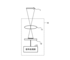
まず、本発明の実施の形態に係る撮像装置について説明する。図1は、実施の形態に係る撮像装置の概略構成を示した側面図である。
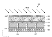
続いて、実施の形態に係る撮像素子12の概略を説明する。図2は、実施の形態に係るレンズ光学系11と、撮像素子12の要部の断面を模式的に示す図である。図2以降では、撮像素子12の一部を、撮像素子100として説明する。撮像素子100は、カラーフィルタ上に、画素アレイの光電変換素子に入射光を導く複数の柱状構造体からなる光学素子を全面に形成した光学素子アレイ(光学素子)を有する。また、撮像素子100では、図2に示すように、レンズ光学系11から撮像素子100に入射する光の入射角度θが、中央部と外周部とで異なるため、光学素子アレイに形成した複数の柱状構造体を、入射光の入射角度に応じて、直下の光電変換素子に導くための位相特性を与える大きさに設定している。以降、図3~図5を用いて、撮像素子100の構造について説明する。
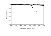
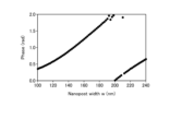
次に、柱状構造体160を側面視したときの高さについて説明する。以降、柱状構造体160を側面視したときの高さを、柱状構造体160の高さと記載する。そして、柱状構造体160の平面視したときの幅を、柱状構造体160の幅と記載する。ここでは、0~2πの位相制御に必要な柱状構造体160の最小高さについて説明する。
柱状構造体160の構造の一例について説明する。図7は、柱状構造体160の側面図である。図8は、柱状構造体160の平面図である。図7及び図8に示すように、例えば、柱状構造体160は、石英によって形成される透明層150uの上面に形成される。そして、柱状構造体160の高さ(z軸方向の長さ)は、h=1000nmとし、柱状構造体160の配置周期は、320nmとする。柱状構造体160の幅wは、0~2πの制御すべき位相に対応させて設定される。
本実施の形態に係る撮像素子100では、入射角に対応して、光学素子アレイ120下方の画素130の中心に集光するように、レンズとして機能する柱状構造体160の位相分布を設計する。そして、撮像素子100では、設計した位相分布となるように、図10の位相特性を参照しながら柱状構造体160の幅wを柱状構造体160ごとに設定することで、設計目標の理想的な位相分布を実現する。
1つの光電変換素子の大きさ=レンズの面積:3.2μm×3.2μm
焦点距離:3.2μm
設計波長:520nm

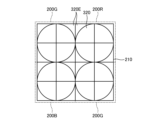
実施の形態では、図5に示す光学素子ユニット120R,120G,120Bのように、対応する直下の画素ユニットの光電変換素子の設計波長に対応させて、光学素子ユニット120R,120G,120Bの各柱状構造体160のパターンを設計する。光学素子ユニットでは、該光学素子ユニットを形成する複数の柱状構造体160の各々の平面視したときの幅wが、該光学素子ユニットが対応する光電変換素子が受光する波長範囲の光を、該光学素子ユニットが対応する光電変換素子に導くための光位相遅延量分布を与える幅に設定されている。そこで、光学素子アレイ120による集光強度の波長依存性について説明する。
本実施の形態では、入射光の入射角度に応じて、光学素子ユニットの各柱状構造体160のパターンを設計する。光学素子ユニットでは、該光学素子ユニットを形成する複数の柱状構造体160の各々の平面視したときの幅wが、入射光の入射角度に応じて、入射光を該光学素子ユニットの直下の光電変換素子に導くための光位相遅延量分布を与える幅に設定されている。そこで、光学素子アレイ120への入射光の入射角度に対応した光学素子ユニットの設計例について説明する。
このように、実施の形態に係る撮像素子100では、複数の柱状構造体160を、入射光の波長よりも短い間隔で、光学素子アレイ120全面に形成することでレンズ機能を実現するため、入射するすべての入射光を受光でき、受光効率の向上を図ることができる。
10 撮像装置
11 レンズ光学系
12,100,100A 撮像素子
13 信号処理部
110 画素アレイ
120,120A 光学素子アレイ
120R,120G,120B,120-1~120-12 光学素子ユニット
130 画素
140L,140R 画素ユニット
150,150A 透明層
160 柱状構造体
170 カラーフィルタ
180 配線層
190 透明基板
Claims (11)
- 光電変換素子を含む画素を覆うための透明層と、
前記透明層上または前記透明層内において前記透明層の面方向に配置され、入射光を、対応する前記光電変換素子に導く複数の柱状構造体と、
を有する光学素子であって、
前記複数の柱状構造体は、前記入射光の波長よりも短い間隔で、前記透明層の全面に形成され、
前記柱状構造体の材料は、複数の前記画素を有する撮像素子を用いる光の波長帯域に応じて、Si、SiN、SiC、TiO2、GaN、GaAs、または、InPの中から選択され、
前記複数の柱状構造体の各々は、前記入射光に対して、平面視したときに当該柱状構造体が有する幅に応じた光位相遅延量を与え、
前記複数の柱状構造体の各々が、対応する前記光電変換素子の設計波長、及び、前記入射光の入射角(θ,φ)に応じて、対応する前記光電変換素子に導くための光位相遅延量分布を与える幅を有し、
前記θは、前記光学素子の平面をxy平面とし、前記入射光が前記光学素子の前記xy平面の原点に入射するとした場合、前記光学素子のxy平面の法線であるz軸と前記入射光との角度であり、
前記φは、前記入射光を、前記光学素子のxy平面に投影した影とx軸との角度であることを特徴とする光学素子。 - 当該光学素子は、平面視したときに、前記複数の柱状構造体が格子状に形成されることを特徴とする請求項1に記載の光学素子。
- 前記複数の柱状構造体は、
前記複数の柱状構造体の周囲材料の屈折率よりも高い屈折率を有し、
平面視したときに、前記複数の柱状構造体のうちの少なくとも一部の柱状構造体は、互いに異なる幅を有し、
側面視したときに、同じ高さを有することを特徴とする請求項1または2に記載の光学素子。 - 前記複数の柱状構造体は、
前記複数の柱状構造体の周囲材料の屈折率よりも高い屈折率を有し、
前記複数の柱状構造体のうちの少なくとも一部の柱状構造体は、互いに異なる屈折率を有し、
側面視したときに、同じ高さを有することを特徴とする請求項1または2に記載の光学素子。 - 当該光学素子は、当該光学素子を構成する複数の柱状構造体の各々の平面視したときの幅が、該光学素子が対応する前記光電変換素子が受光する波長範囲の光を、当該光学素子が対応する光電変換素子に導くための光位相遅延量分布を与える幅に設定されていることを特徴とする請求項1に記載の光学素子。
- 前記複数の柱状構造体は、各々の平面視したときの幅が、前記対応する光電変換素子における波長範囲ごとに異なる値に設定されていることを特徴とする請求項5に記載の光学素子。
- 前記光位相遅延量分布は、光を集光するための光位相遅延量であることを特徴とする請求項5または6に記載の光学素子。
- 前記複数の柱状構造体は、前記透明層の屈折率よりも高い屈折率を有する材料を用いて形成されることを特徴とする請求項1~7のいずれか一つに記載の光学素子。
- 前記複数の柱状構造体は、平面視したときに、4回回転対称構造であることを特徴とする請求項1~8のいずれか一つに記載の光学素子。
- 請求項1~9のいずれか一つに記載の光学素子と、
各々が前記光電変換素子を含む複数の画素と、
を有することを特徴とする撮像素子。 - 請求項10に記載の撮像素子と、
前記撮像素子が出力する電気信号を処理し、画像を生成する信号処理部と、
を有することを特徴とする撮像装置。
Applications Claiming Priority (1)
| Application Number | Priority Date | Filing Date | Title |
|---|---|---|---|
| PCT/JP2020/038499 WO2022079765A1 (ja) | 2020-10-12 | 2020-10-12 | 光学素子、撮像素子及び撮像装置 |
Publications (2)
| Publication Number | Publication Date |
|---|---|
| JPWO2022079765A1 JPWO2022079765A1 (ja) | 2022-04-21 |
| JP7635787B2 true JP7635787B2 (ja) | 2025-02-26 |
Family
ID=81207794
Family Applications (1)
| Application Number | Title | Priority Date | Filing Date |
|---|---|---|---|
| JP2022557237A Active JP7635787B2 (ja) | 2020-10-12 | 2020-10-12 | 光学素子、撮像素子及び撮像装置 |
Country Status (5)
| Country | Link |
|---|---|
| US (1) | US20230378211A1 (ja) |
| EP (1) | EP4227715A4 (ja) |
| JP (1) | JP7635787B2 (ja) |
| CN (1) | CN116368406B (ja) |
| WO (1) | WO2022079765A1 (ja) |
Families Citing this family (3)
| Publication number | Priority date | Publication date | Assignee | Title |
|---|---|---|---|---|
| WO2024162113A1 (ja) * | 2023-02-03 | 2024-08-08 | ソニーセミコンダクタソリューションズ株式会社 | 光検出装置、光学素子、および電子機器 |
| WO2025079513A1 (ja) * | 2023-10-11 | 2025-04-17 | ソニーセミコンダクタソリューションズ株式会社 | 撮像装置及び電子機器 |
| US20250297855A1 (en) * | 2024-03-21 | 2025-09-25 | Kla Corporation | System and method for device-like overlay targets measurement |
Citations (6)
| Publication number | Priority date | Publication date | Assignee | Title |
|---|---|---|---|---|
| JP2009157390A (ja) | 2004-09-01 | 2009-07-16 | Panasonic Corp | 固体撮像装置 |
| JP2010212625A (ja) | 2009-03-12 | 2010-09-24 | Nikon Corp | 固体撮像素子 |
| JP2011040441A (ja) | 2009-08-06 | 2011-02-24 | Panasonic Corp | 固体撮像装置 |
| US20170034500A1 (en) | 2015-07-29 | 2017-02-02 | Samsung Electronics Co., Ltd. | Imaging apparatus and image sensor including the same |
| JP2019184986A (ja) | 2018-04-17 | 2019-10-24 | 日本電信電話株式会社 | カラー撮像素子および撮像装置 |
| JP2020051868A (ja) | 2018-09-26 | 2020-04-02 | 日本電信電話株式会社 | 偏光イメージング撮像システム |
Family Cites Families (19)
| Publication number | Priority date | Publication date | Assignee | Title |
|---|---|---|---|---|
| GB2256477B (en) * | 1991-06-07 | 1995-03-08 | Marconi Gec Ltd | An optical sensor |
| CN100463200C (zh) * | 2004-02-03 | 2009-02-18 | 松下电器产业株式会社 | 固体摄像装置及其制造方法以及照相机 |
| US7674737B2 (en) * | 2004-06-22 | 2010-03-09 | Nippon Telegraph And Telephone Corporation | Optical medium, an optical lens and a prism |
| JP4929780B2 (ja) * | 2006-03-24 | 2012-05-09 | 住友化学株式会社 | 液晶表示装置及びそれに用いる防眩性偏光フィルム積層体 |
| US8213085B2 (en) * | 2008-01-18 | 2012-07-03 | Visera Technologies Company Limited | Image sensor device with high photosensitivity |
| WO2009104390A1 (ja) * | 2008-02-22 | 2009-08-27 | パナソニック株式会社 | 撮像装置 |
| JP2012064703A (ja) * | 2010-09-15 | 2012-03-29 | Sony Corp | 撮像素子および撮像装置 |
| JP2012084608A (ja) | 2010-10-07 | 2012-04-26 | Sony Corp | 固体撮像装置とその製造方法、並びに電子機器 |
| KR101853817B1 (ko) * | 2011-07-20 | 2018-05-02 | 삼성전자주식회사 | 촬상 소자 |
| JP5337212B2 (ja) * | 2011-09-02 | 2013-11-06 | 株式会社東芝 | 固体撮像素子 |
| JP5456084B2 (ja) * | 2012-02-07 | 2014-03-26 | 株式会社東芝 | 固体撮像素子 |
| US11378797B2 (en) * | 2015-04-08 | 2022-07-05 | Samsung Electronics Co., Ltd. | Focusing device comprising a plurality of scatterers and beam scanner and scope device |
| US11089286B2 (en) * | 2015-07-29 | 2021-08-10 | Samsung Electronics Co., Ltd. | Image sensor |
| JP6706482B2 (ja) * | 2015-11-05 | 2020-06-10 | ソニーセミコンダクタソリューションズ株式会社 | 固体撮像装置および電子機器 |
| JP2018201061A (ja) * | 2017-05-25 | 2018-12-20 | ソニーセミコンダクタソリューションズ株式会社 | 固体撮像装置 |
| CN107357048B (zh) * | 2017-08-03 | 2019-05-03 | 南开大学 | 傅里叶透镜、傅里叶透镜设计方法及纹影仪 |
| CN110972505B (zh) * | 2018-09-21 | 2023-10-27 | 深圳市汇顶科技股份有限公司 | 影像感测器及半导体结构 |
| US11698296B2 (en) * | 2019-09-25 | 2023-07-11 | Stmicroelectronics (Crolles 2) Sas | Light sensor using pixel optical diffraction gratings having different pitches |
| KR102868992B1 (ko) * | 2019-10-10 | 2025-10-10 | 삼성전자주식회사 | 줌 가능한 이미지 센서 및 이미지 센싱 방법 |
-
2020
- 2020-10-12 JP JP2022557237A patent/JP7635787B2/ja active Active
- 2020-10-12 CN CN202080106082.1A patent/CN116368406B/zh active Active
- 2020-10-12 WO PCT/JP2020/038499 patent/WO2022079765A1/ja not_active Ceased
- 2020-10-12 US US18/031,157 patent/US20230378211A1/en active Pending
- 2020-10-12 EP EP20957594.3A patent/EP4227715A4/en active Pending
Patent Citations (6)
| Publication number | Priority date | Publication date | Assignee | Title |
|---|---|---|---|---|
| JP2009157390A (ja) | 2004-09-01 | 2009-07-16 | Panasonic Corp | 固体撮像装置 |
| JP2010212625A (ja) | 2009-03-12 | 2010-09-24 | Nikon Corp | 固体撮像素子 |
| JP2011040441A (ja) | 2009-08-06 | 2011-02-24 | Panasonic Corp | 固体撮像装置 |
| US20170034500A1 (en) | 2015-07-29 | 2017-02-02 | Samsung Electronics Co., Ltd. | Imaging apparatus and image sensor including the same |
| JP2019184986A (ja) | 2018-04-17 | 2019-10-24 | 日本電信電話株式会社 | カラー撮像素子および撮像装置 |
| JP2020051868A (ja) | 2018-09-26 | 2020-04-02 | 日本電信電話株式会社 | 偏光イメージング撮像システム |
Also Published As
| Publication number | Publication date |
|---|---|
| EP4227715A1 (en) | 2023-08-16 |
| WO2022079765A1 (ja) | 2022-04-21 |
| CN116368406A (zh) | 2023-06-30 |
| EP4227715A4 (en) | 2024-06-12 |
| CN116368406B (zh) | 2025-10-28 |
| JPWO2022079765A1 (ja) | 2022-04-21 |
| US20230378211A1 (en) | 2023-11-23 |
Similar Documents
| Publication | Publication Date | Title |
|---|---|---|
| JP7563473B2 (ja) | 撮像素子及び撮像装置 | |
| KR102389008B1 (ko) | 컬러촬상소자 및 촬상장치 | |
| CN100492064C (zh) | 聚光元件以及固体摄像装置 | |
| JP7635787B2 (ja) | 光学素子、撮像素子及び撮像装置 | |
| JP7574860B2 (ja) | 撮像素子及び撮像装置 | |
| JP7773081B2 (ja) | 分光素子アレイ、撮像素子および撮像装置 | |
| JP7574859B2 (ja) | 撮像素子及び撮像装置 | |
| US20250120207A1 (en) | Image capturing element and image capturing apparatus having spectroscopic element array | |
| JP7574858B2 (ja) | 撮像素子及び撮像装置 | |
| JP7265195B2 (ja) | カラー撮像素子および撮像装置 | |
| JP2025010437A (ja) | カラー撮像素子および撮像装置 | |
| WO2025258002A1 (ja) | 撮像素子および撮像装置 | |
| WO2023021632A1 (ja) | 光学素子、撮像素子及び撮像装置 |
Legal Events
| Date | Code | Title | Description |
|---|---|---|---|
| A621 | Written request for application examination |
Free format text: JAPANESE INTERMEDIATE CODE: A621 Effective date: 20230131 |
|
| A131 | Notification of reasons for refusal |
Free format text: JAPANESE INTERMEDIATE CODE: A131 Effective date: 20240326 |
|
| A521 | Request for written amendment filed |
Free format text: JAPANESE INTERMEDIATE CODE: A523 Effective date: 20240522 |
|
| A131 | Notification of reasons for refusal |
Free format text: JAPANESE INTERMEDIATE CODE: A131 Effective date: 20240827 |
|
| A521 | Request for written amendment filed |
Free format text: JAPANESE INTERMEDIATE CODE: A523 Effective date: 20241001 |
|
| TRDD | Decision of grant or rejection written | ||
| A01 | Written decision to grant a patent or to grant a registration (utility model) |
Free format text: JAPANESE INTERMEDIATE CODE: A01 Effective date: 20250114 |
|
| A61 | First payment of annual fees (during grant procedure) |
Free format text: JAPANESE INTERMEDIATE CODE: A61 Effective date: 20250127 |
|
| R150 | Certificate of patent or registration of utility model |
Ref document number: 7635787 Country of ref document: JP Free format text: JAPANESE INTERMEDIATE CODE: R150 |
|
| S533 | Written request for registration of change of name |
Free format text: JAPANESE INTERMEDIATE CODE: R313533 |
|
| R350 | Written notification of registration of transfer |
Free format text: JAPANESE INTERMEDIATE CODE: R350 |