JP7635787B2 - Optical element, imaging element, and imaging device - Google Patents
Optical element, imaging element, and imaging device Download PDFInfo
- Publication number
- JP7635787B2 JP7635787B2 JP2022557237A JP2022557237A JP7635787B2 JP 7635787 B2 JP7635787 B2 JP 7635787B2 JP 2022557237 A JP2022557237 A JP 2022557237A JP 2022557237 A JP2022557237 A JP 2022557237A JP 7635787 B2 JP7635787 B2 JP 7635787B2
- Authority
- JP
- Japan
- Prior art keywords
- optical element
- columnar structures
- light
- columnar
- photoelectric conversion
- Prior art date
- Legal status (The legal status is an assumption and is not a legal conclusion. Google has not performed a legal analysis and makes no representation as to the accuracy of the status listed.)
- Active
Links
Images


Classifications
-
- H—ELECTRICITY
- H10—SEMICONDUCTOR DEVICES; ELECTRIC SOLID-STATE DEVICES NOT OTHERWISE PROVIDED FOR
- H10F—INORGANIC SEMICONDUCTOR DEVICES SENSITIVE TO INFRARED RADIATION, LIGHT, ELECTROMAGNETIC RADIATION OF SHORTER WAVELENGTH OR CORPUSCULAR RADIATION
- H10F39/00—Integrated devices, or assemblies of multiple devices, comprising at least one element covered by group H10F30/00, e.g. radiation detectors comprising photodiode arrays
- H10F39/80—Constructional details of image sensors
- H10F39/806—Optical elements or arrangements associated with the image sensors
- H10F39/8063—Microlenses
-
- G—PHYSICS
- G02—OPTICS
- G02B—OPTICAL ELEMENTS, SYSTEMS OR APPARATUS
- G02B3/00—Simple or compound lenses
- G02B3/0006—Arrays
- G02B3/0037—Arrays characterized by the distribution or form of lenses
- G02B3/0056—Arrays characterized by the distribution or form of lenses arranged along two different directions in a plane, e.g. honeycomb arrangement of lenses
-
- G—PHYSICS
- G02—OPTICS
- G02B—OPTICAL ELEMENTS, SYSTEMS OR APPARATUS
- G02B5/00—Optical elements other than lenses
- G02B5/18—Diffraction gratings
- G02B5/1809—Diffraction gratings with pitch less than or comparable to the wavelength
-
- G—PHYSICS
- G02—OPTICS
- G02B—OPTICAL ELEMENTS, SYSTEMS OR APPARATUS
- G02B6/00—Light guides; Structural details of arrangements comprising light guides and other optical elements, e.g. couplings
- G02B6/10—Light guides; Structural details of arrangements comprising light guides and other optical elements, e.g. couplings of the optical waveguide type
- G02B6/12—Light guides; Structural details of arrangements comprising light guides and other optical elements, e.g. couplings of the optical waveguide type of the integrated circuit kind
- G02B6/122—Basic optical elements, e.g. light-guiding paths
- G02B6/1223—Basic optical elements, e.g. light-guiding paths high refractive index type, i.e. high-contrast waveguides
-
- H—ELECTRICITY
- H10—SEMICONDUCTOR DEVICES; ELECTRIC SOLID-STATE DEVICES NOT OTHERWISE PROVIDED FOR
- H10F—INORGANIC SEMICONDUCTOR DEVICES SENSITIVE TO INFRARED RADIATION, LIGHT, ELECTROMAGNETIC RADIATION OF SHORTER WAVELENGTH OR CORPUSCULAR RADIATION
- H10F30/00—Individual radiation-sensitive semiconductor devices in which radiation controls the flow of current through the devices, e.g. photodetectors
- H10F30/20—Individual radiation-sensitive semiconductor devices in which radiation controls the flow of current through the devices, e.g. photodetectors the devices having potential barriers, e.g. phototransistors
- H10F30/21—Individual radiation-sensitive semiconductor devices in which radiation controls the flow of current through the devices, e.g. photodetectors the devices having potential barriers, e.g. phototransistors the devices being sensitive to infrared, visible or ultraviolet radiation
-
- H—ELECTRICITY
- H10—SEMICONDUCTOR DEVICES; ELECTRIC SOLID-STATE DEVICES NOT OTHERWISE PROVIDED FOR
- H10F—INORGANIC SEMICONDUCTOR DEVICES SENSITIVE TO INFRARED RADIATION, LIGHT, ELECTROMAGNETIC RADIATION OF SHORTER WAVELENGTH OR CORPUSCULAR RADIATION
- H10F39/00—Integrated devices, or assemblies of multiple devices, comprising at least one element covered by group H10F30/00, e.g. radiation detectors comprising photodiode arrays
- H10F39/80—Constructional details of image sensors
- H10F39/802—Geometry or disposition of elements in pixels, e.g. address-lines or gate electrodes
- H10F39/8023—Disposition of the elements in pixels, e.g. smaller elements in the centre of the imager compared to larger elements at the periphery
-
- H—ELECTRICITY
- H10—SEMICONDUCTOR DEVICES; ELECTRIC SOLID-STATE DEVICES NOT OTHERWISE PROVIDED FOR
- H10F—INORGANIC SEMICONDUCTOR DEVICES SENSITIVE TO INFRARED RADIATION, LIGHT, ELECTROMAGNETIC RADIATION OF SHORTER WAVELENGTH OR CORPUSCULAR RADIATION
- H10F39/00—Integrated devices, or assemblies of multiple devices, comprising at least one element covered by group H10F30/00, e.g. radiation detectors comprising photodiode arrays
- H10F39/80—Constructional details of image sensors
- H10F39/806—Optical elements or arrangements associated with the image sensors
- H10F39/8067—Reflectors
Landscapes
- Physics & Mathematics (AREA)
- General Physics & Mathematics (AREA)
- Optics & Photonics (AREA)
- Engineering & Computer Science (AREA)
- Microelectronics & Electronic Packaging (AREA)
- Solid State Image Pick-Up Elements (AREA)
- Transforming Light Signals Into Electric Signals (AREA)
Description
本発明は、光学素子、撮像素子及び撮像装置に関する。 The present invention relates to an optical element, an imaging element, and an imaging device.
一般的な撮像装置は、レンズ光学系と、CCD(Charge Coupled Device)センサやCMOS(Complementary Metal Oxide Semiconductor)センサなどの2次元撮像素子とを用いて、撮像対象からの光の強度情報と色情報からなる2次元画像を取得する。A typical imaging device uses a lens optical system and a two-dimensional imaging element such as a CCD (Charge Coupled Device) sensor or a CMOS (Complementary Metal Oxide Semiconductor) sensor to obtain a two-dimensional image consisting of light intensity information and color information from the subject.
撮像装置では、光電変換素子を含む各画素上で入射光の色分離を行うため、2次元アレイ状に配列された光電変換素子を含む画素を有する画素アレイ上に、各画素に対応したカラーフィルタが設けられる。そして、撮像装置では、感度特性の向上のために、カラーフィルタ上にオンチップマイクロレンズ(以降、オンチップレンズとする。)を形成し、入射したオンチップレンズにより光電変換素子に集光させている。In an imaging device, in order to perform color separation of incident light on each pixel containing a photoelectric conversion element, a color filter corresponding to each pixel is provided on a pixel array having pixels containing photoelectric conversion elements arranged in a two-dimensional array. In order to improve sensitivity characteristics, the imaging device forms an on-chip microlens (hereinafter referred to as an on-chip lens) on the color filter, and the incident light is focused on the photoelectric conversion element by the on-chip lens.
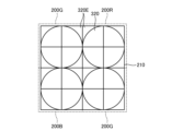
図25及び図26は、オンチップレンズの平面図である。図25及び図26に示すように、画素アレイ210の各画素200R,200G,200B上には、オンチップレンズ220またはオンチップレンズ320がそれぞれ形成される。しかしながら、オンチップレンズ220間、オンチップレンズ320間には、隙間220E,320E等がある。このレンズ間の隙間220E,320E等のレンズ開口領域外に入射した光は光電変換素子に効果的に集光できないため、従来のオンチップレンズ220,320では、すべての入射光を受光できず、受光効率が制限される。25 and 26 are plan views of an on-chip lens. As shown in FIG. 25 and FIG. 26, an on-
本発明は、上記に鑑みてなされたものであって、従来と比して、受光効率を向上させることができる光学素子、撮像素子及び撮像装置を提供することを目的とする。The present invention has been made in consideration of the above, and aims to provide an optical element, an imaging element, and an imaging device that can improve light receiving efficiency compared to conventional techniques.
上述した課題を解決し、目的を達成するために、本発明に係る光学素子は、光電変換素子を含む画素を覆うための透明層と、透明層上または透明層内において透明層の面方向に配置され、入射光を、対応する光電変換素子に導く複数の柱状構造体と、を有し、複数の柱状構造体は、入射光の波長よりも短い間隔で、透明層の全面に形成されることを特徴とする。In order to solve the above-mentioned problems and achieve the object, the optical element of the present invention has a transparent layer for covering pixels including photoelectric conversion elements, and a plurality of columnar structures arranged on or within the transparent layer in the planar direction of the transparent layer and directing incident light to corresponding photoelectric conversion elements, the plurality of columnar structures being formed over the entire surface of the transparent layer at intervals shorter than the wavelength of the incident light.
また、本発明に係る撮像素子は、上記記載の光学素子と、各々が光電変換素子を含む複数の画素と、を有することを特徴とする。 The imaging element of the present invention is characterized by having the optical element described above and a plurality of pixels, each of which includes a photoelectric conversion element.
また、本発明に係る撮像装置は、上記記載の撮像素子と、撮像素子が出力する電気信号を処理し、画像を生成する信号処理部と、を有することを特徴とする。 The imaging device according to the present invention is characterized in having the imaging element described above and a signal processing unit that processes the electrical signal output by the imaging element and generates an image.
本発明によれば、従来と比して、受光効率を向上させることができる撮像素子及び撮像装置を提供することができる。 According to the present invention, it is possible to provide an imaging element and an imaging device that can improve the light receiving efficiency compared to the conventional art.
以下、本発明を実施するための最良の形態を図面とともに詳細に説明する。なお、以下の説明において、各図は本発明の内容を理解でき得る程度に形状、大きさ、及び位置関係を概略的に示してあるに過ぎず、したがって、本発明は各図で例示された形状、大きさ、及び位置関係のみに限定されるものではない。また、図面の記載において、同一部分には同一の符号を付して示している。The best mode for carrying out the present invention will be described in detail below with reference to the drawings. In the following description, each figure merely shows the shape, size, and positional relationship in a schematic manner to enable the content of the present invention to be understood, and therefore the present invention is not limited to only the shape, size, and positional relationship exemplified in each figure. In addition, in the description of the drawings, the same parts are denoted by the same reference numerals.
[実施の形態]
[撮像装置]
まず、本発明の実施の形態に係る撮像装置について説明する。図1は、実施の形態に係る撮像装置の概略構成を示した側面図である。
[Embodiment]
[Imaging device]
First, an image pickup apparatus according to an embodiment of the present invention will be described with reference to Fig. 1. Fig. 1 is a side view showing a schematic configuration of an image pickup apparatus according to an embodiment of the present invention.
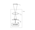
図1に示すように、実施の形態に係る撮像装置10は、レンズ光学系11、撮像素子12及び信号処理部13を有する。撮像素子12は、CCDやCMOS等の光電変換素子を有する。信号処理部13は、撮像素子12から出力される光電変換信号を処理して画像信号を生成する。1, an
自然光や照明光等の光が物体1に照射され、物体1により透過/反射/散乱した光、または、物体1から発する光は、レンズ光学系11により撮像素子12上に光学像を形成する。一般に、レンズ光学系11は、様々な光学収差を補正するため、光軸に沿って並んだ複数のレンズからなるレンズ群により構成されるが、図1では図面を簡略化して単一のレンズとして示している。信号処理部13は、生成した画像信号を外部に送出する画像信号出力を有する。
Natural light, illumination light, or other light is irradiated onto object 1, and the light transmitted/reflected/scattered by object 1, or the light emitted from object 1, forms an optical image on
なお、撮像装置10は、赤外光カットの光学フィルタ、電子シャッタ、ビューファインダ、電源(電池)、フラッシュライトなどの公知の構成要素を備え得るが、それらの説明は、本発明の理解に特に必要でないため省略する。また、以上の構成はあくまでも一例であり、実施の形態では、レンズ光学系11、撮像素子12、信号処理部13を除く構成要素として、公知の要素を適切に組み合わせて用いることができる。The
[撮像素子]
続いて、実施の形態に係る撮像素子12の概略を説明する。図2は、実施の形態に係るレンズ光学系11と、撮像素子12の要部の断面を模式的に示す図である。図2以降では、撮像素子12の一部を、撮像素子100として説明する。撮像素子100は、カラーフィルタ上に、画素アレイの光電変換素子に入射光を導く複数の柱状構造体からなる光学素子を全面に形成した光学素子アレイ(光学素子)を有する。また、撮像素子100では、図2に示すように、レンズ光学系11から撮像素子100に入射する光の入射角度θが、中央部と外周部とで異なるため、光学素子アレイに形成した複数の柱状構造体を、入射光の入射角度に応じて、直下の光電変換素子に導くための位相特性を与える大きさに設定している。以降、図3~図5を用いて、撮像素子100の構造について説明する。
[Image sensor]
Next, an outline of the
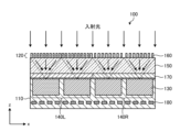
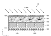
図3は、実施の形態に係る撮像素子の中央部における画素アレイ及び光学素子アレイの断面の一部を模式的に示す図である。図4は、実施の形態に係る撮像素子の外周部における画素アレイ及び光学素子アレイの断面の一部を模式的に示す図である。図5は、実施の形態に係る撮像素子の中央部における光学素子アレイの上面図である。 Figure 3 is a schematic diagram showing a portion of a cross section of a pixel array and an optical element array in the center of an imaging element relating to an embodiment. Figure 4 is a schematic diagram showing a portion of a cross section of a pixel array and an optical element array in the outer periphery of an imaging element relating to an embodiment. Figure 5 is a top view of an optical element array in the center of an imaging element relating to an embodiment.
図3及び図4に示すように、撮像素子100は、画素アレイ110と、画素アレイ110と対向して配置された光学素子アレイ120とを有する。光学素子アレイ120は、レンズ光学系11からの光が入射する側に配置されている。光学素子アレイ120は、画素アレイ110上に形成された透明層150の上面に形成される。画素アレイ110上には、各画素に対応したカラーフィルタ170が設けられる。なお、透明層150は、SiO2(屈折率n=1.45)等の材料からなる低屈折率の透明層である。
3 and 4, the
画素アレイ110は、配線層180と、2次元アレイ状に配列された光電変換素子を含む画素130とを有する。画素ユニット140Lの画素130は、例えば、G光を受光し、画素ユニット140Rの画素130は、R光を受光する。The
光学素子アレイ120は、入射光を、対応する直下の画素130の光電変換素子に導く複数の柱状構造体160からなる光学素子が2次元アレイ状に配列される。例えば、図5では、カラーフィルタ170が分離する波長領域が赤(R)、緑(G)、青(B)である場合について示す。図5の光学素子アレイ120では、画素アレイ110上の、R光を受光するR画素ユニット、G光を受光する2つのG画素ユニット及びB光を受光するB画素ユニットがそれぞれ直下に位置するように配置された、R画素ユニットに対応する光学素子ユニット120R(光学素子)、G画素ユニットに対応する2つの光学素子ユニット120G(光学素子)、B画素ユニットに対応する光学素子ユニット120B(光学素子)を1組とした光学素子ユニットが2次元アレイ上に形成される。In the
複数の柱状構造体160は、周囲材料(透明層150、空気)の屈折率よりも高い屈折率を有する材料を用いて形成される。これによって、柱状構造体160は、柱状構造体内部に光を強く閉じ込めて隣接する柱状構造体との光結合を防ぐ。柱状構造体160は、例えば、SiN(屈折率n=2.05)、TiO2(屈折率n=2.4)を用いて形成される。
The plurality of
複数の柱状構造体160は、図3及び図4に示すように、側面視したときに、同じ高さに形成される。複数の柱状構造体160は、入射光の波長よりも短い間隔で、光学素子アレイ120全面に形成される。図5に示すように、光学素子ユニット120R,120G,120Bは、平面視したときに、複数の柱状構造体160が格子状に形成される。複数の柱状構造体160は、角柱である。なお、図5の例は一例であり、柱状構造体は、平面視したときに、中空正方形、円形、中空円形または十字形上のような4回回転対象となる構造体を採用してもよい。
As shown in Figures 3 and 4, the multiple
複数の柱状構造体160は、平面視したときに、各柱状構造体の入射光の入射角度に応じて、入射光を、対応する直下の画素130の光電変換素子に導くための位相特性を有する幅wにそれぞれ形成される。複数の柱状構造体160の各々は、入射光に対して、平面視したときに当該柱状構造体160が有する幅に応じた光位相遅延量を与える。Each of the plurality of
光学素子ユニット120R,120G,120Bでは、該光学素子ユニット120R,120G,120Bを構成する複数の柱状構造体160の各々が、入射光を、対応するR画素ユニット、G画素ユニット、B画素ユニットの各光電変換素子に導くための光位相遅延量分布を与える幅を有する。光学素子ユニット120R,120G,120Bでは、該光学素子ユニット120R,120G,120Bを形成する複数の柱状構造体160の各々の平面視したときの幅が、入射光の入射角度に応じて、入射光を該光学素子ユニット120R,120G,120Bの直下の光電変換素子に導くための光位相遅延量分布を与える幅に設定されている。なお、光位相遅延量分布は、光を集光するための光位相遅延量である。In the
撮像素子100は、高さが同一で、幅が徐々に変換する柱状構造体160を、光学素子アレイ120全面に形成することで、レンズ機能を実現する。各柱状構造体160は、柱状の光導波路のように振る舞うため、撮像素子100では、柱状構造体160の幅を変化させることで、柱状構造体160の有効屈折率を変化させて、透過する光の位相を自由に制御することができる。The
言い換えると、各柱状構造体160は、サブ波長サイズの光導波路として振る舞い、かつ、光閉じ込めにより隣接する柱状構造体160との光結合がほとんどないため、柱状構造体160の平面視した際の幅wをそれぞれ柱状構造体160ごとに設計することで、複数の柱状構造体160毎に異なる光学特性(例えば位相遅延特性)を与えることが可能である。この位相遅延量の空間分布を(フレネル)レンズと同等のものにすることで、柱状構造体160にレンズ機能を付与することができる。In other words, each
ここで、非特許文献1には、SiO2等の低屈折材料からなる構造体をレンズとして機能させることが記載されている。 Here, Non-Patent Document 1 describes that a structure made of a low refractive index material such as SiO2 is made to function as a lens.
非特許文献1では、構造体が波長に比べて非常に小さい場合、構造体の有効屈折率が構造レンズと周囲材料の屈折率とのほぼ平均値で表すことができるという近似が記載されている。しかしながら、構造体の屈折率と周囲の屈折率の差が大きくかつ構造体の大きさがサブ波長程度の場合、光が構造内部に閉じ込められて光導波路モードや共振モードを励起してしまうため、この近似は適用できなくなる。このため、非特許文献1記載の構造体は、材料をSiO2とし、周囲材料を空気などとする、屈折率差が小さい材料の組み合わせに限定されるため、構造体のアスペクト比が大きくなる。 In Non-Patent Document 1, an approximation is described that when the structure is very small compared to the wavelength, the effective refractive index of the structure can be expressed by approximately the average value of the refractive index of the structural lens and the surrounding material. However, when the difference between the refractive index of the structure and the surrounding refractive index is large and the size of the structure is about sub-wavelength, this approximation cannot be applied because the light is confined inside the structure and excites the optical waveguide mode or the resonance mode. For this reason, the structure described in Non-Patent Document 1 is limited to a combination of materials with a small refractive index difference, such as SiO 2 as the material and air as the surrounding material, and the aspect ratio of the structure becomes large.
これに対し、撮像素子100では、各柱状構造体160を、SiNやTiO2などの高屈折率材料を用いて形成している。このため、位相変化量0~2πを実現するために必要な最小の柱状構造体160の高さが、SiO2等の低屈折材料からなる構造体(非特許文献1参照)と比して、低い。したがって、撮像素子100は、0~2πの位相制御に必要な最小構造高さが比較的小さく、作製しやすい低アスペクト比の柱状構造体160でレンズ機能を実現できる。
In contrast, in the
そして、複数の柱状構造体160は、底面が正方形の角柱である。このように、撮像素子100では、各柱状構造体160を、平面視したときに、正方形などの4回回転対称構造にすることで、偏光に対して無依存な特性とする。なお、非特許文献1記載の構造体は、理論式により有効屈折率に偏光依存性を有することが明らかである。The multiple
また、非特許文献1には、曲面及びステップを有する構造体が記載されている。これに対し、本実施の形態における各柱状構造体160は、段差のない角柱状のバイナリパターンである。したがって、撮像素子100は、柱状構造体の断面から曲面及びステップを排除できるため、非特許文献1に記載の構造体と比して、柱状構造体160の作成が比較的容易である。Furthermore, Non-Patent Document 1 describes a structure having curved surfaces and steps. In contrast, each
また、撮像素子100は、複数の柱状構造体160を、光学素子アレイ120全面に形成することで、レンズ機能を実現するため、入射するすべての入射光を受光でき、レンズ開口を最大化することができる。
In addition, the
また、各柱状構造体160は、平面視したときに、各柱状構造体160の入射光の入射角度に応じて、直下の画素130の光電変換素子に導く位相特性を有する幅wにそれぞれ形成される。すなわち、撮像素子100では、主入射角に応じて、画素毎に柱状構造体160の構造パターンを受光効率向上に向けて最適化することが可能である。言い換えると、撮像素子100では、柱状構造体160の平面視した際の形状パターンを、各柱状構造体160に入射する光の入射角度θに応じて最適化している。In addition, each
これによって、撮像素子100では、大きな入射角度θで光が入射する外周部(図4参照)と、垂直に光が入射する中央部(図3参照)とのいずれにおいても、柱状構造体160が直下の画素130の光電変換素子に集光できるようになる。したがって、撮像素子100は、多くの光を直下の光電変換素子に集光することができ、撮像素子100全体で均一な輝度をもつ画像信号を生成できる。As a result, in the
[柱状構造体の高さ]
次に、柱状構造体160を側面視したときの高さについて説明する。以降、柱状構造体160を側面視したときの高さを、柱状構造体160の高さと記載する。そして、柱状構造体160の平面視したときの幅を、柱状構造体160の幅と記載する。ここでは、0~2πの位相制御に必要な柱状構造体160の最小高さについて説明する。
[Height of columnar structure]
Next, the height of the
柱状構造体160による位相遅延量φは、光の真空中での波長をλ、柱状構造体160の高さをh、柱状構造体160の有効屈折率neff、周囲材料の屈折率をn0とすると、式(1)で表される。
The phase delay amount φ due to the
![]()
![]()
撮像素子100における柱状構造体160においても、非特許文献1に記載の構造体(以降、有効媒体近似構造体とする。)においても、式(1)が適用される。Equation (1) applies to both the
有効媒質近似構造体の場合、有効屈折率neffは、構造体と周囲材料との面積比で決まることが知られている。有効媒質近似構造体の場合には、偏光によってもneffの値が変動する。そして、柱状構造体160の場合は、光導波路モードが柱状構造体160の幅に大きく依存するため、有効屈折率neffは、柱状構造体160の幅wの関数で表されることが知られている。有効媒質近似構造体、柱状構造体160のいずれの場合でも、n0<neff<n1の値をとる。なお、n1は、構造体を組成する材料の屈折率である。
In the case of an effective medium approximation structure, it is known that the effective refractive index n eff is determined by the area ratio between the structure and the surrounding material. In the case of an effective medium approximation structure, the value of n eff also varies depending on the polarization. In the case of the
したがって、位相変化量を0~2πの間で制御するためには、構造体の高さは、式(2)とする必要がある。 Therefore, in order to control the amount of phase change between 0 and 2π, the height of the structure must be as expressed by equation (2).
![]()
![]()
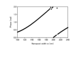
図6は、従来技術における有媒質近似構造体と実施の形態における柱状構造体160との最小構造高さ及び最大アスペクト比を示す図である。図6では、光の波長が635nmである際の最小構造幅を100nmとして、最大アスペクト比を求めている。
Figure 6 is a diagram showing the minimum structural height and maximum aspect ratio of a medium-approximated structure in the prior art and the
有効媒質近似を適用するには、n1-n0を小さくする必要がある。このため、有効媒質近似構造体の場合、必要な構造体の高さは、図6のように1411nmと必然的に高くなり、数波長程度必要となる。 To apply the effective medium approximation, it is necessary to make n 1 −n 0 small. Therefore, in the case of an effective medium approximation structure, the height of the structure required is inevitably as high as 1411 nm as shown in FIG.
これに対し、柱状構造体160の場合、n1が大きい方が光閉じ込めの観点で望ましいため、有効媒質近似構造体よりもn1-n0の値が大きくなる。例えば、柱状構造体160を形成する材料は、SiN(n=2.05)、TiO2(n=2.4)であり、n1-n0≧0.7となる。
In contrast, in the case of the
これによって、柱状構造体160では、必要な構造高さは、有効媒質近似構造体よりも比較的低くなり、図6に示すように、一般的に1波長以下である。このように、柱状構造体160のアスペクト比は、有効媒質近似構造体よりも、低くなる。
As a result, the required structural height of the
[柱状構造体の構造]
柱状構造体160の構造の一例について説明する。図7は、柱状構造体160の側面図である。図8は、柱状構造体160の平面図である。図7及び図8に示すように、例えば、柱状構造体160は、石英によって形成される透明層150uの上面に形成される。そして、柱状構造体160の高さ(z軸方向の長さ)は、h=1000nmとし、柱状構造体160の配置周期は、320nmとする。柱状構造体160の幅wは、0~2πの制御すべき位相に対応させて設定される。
[Structure of columnar structure]
An example of the structure of the
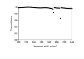
図9は、柱状構造体160の幅wと光の透過率との関係を示す図である。図10は、柱状構造体160の幅wと、柱状構造体160の光の位相特性との関係を示す図である。
Figure 9 is a diagram showing the relationship between the width w of the
図9に示すように、柱状構造体160の幅wを100~240nmの間で変更した場合であっても、高い透過率を保持することができる。そして、柱状構造体160の幅wを100~240nmの間で調整することで、柱状構造体160を透過する光の位相を、0~2πの間の所望の位相に制御することができる。なお、図9及び図10では、柱状構造体160の幅を100nmまで小さくした場合であっても、柱状構造体160のアスペクト比の最大値を10に抑えることができる。As shown in Figure 9, high transmittance can be maintained even when the width w of the
[レンズの設計]
本実施の形態に係る撮像素子100では、入射角に対応して、光学素子アレイ120下方の画素130の中心に集光するように、レンズとして機能する柱状構造体160の位相分布を設計する。そして、撮像素子100では、設計した位相分布となるように、図10の位相特性を参照しながら柱状構造体160の幅wを柱状構造体160ごとに設定することで、設計目標の理想的な位相分布を実現する。
[Lens design]
In the
例えば、以下に設計例のパラメータを示す。
1つの光電変換素子の大きさ=レンズの面積:3.2μm×3.2μm
焦点距離:3.2μm
設計波長:520nm
For example, the parameters of a design example are shown below.
Size of one photoelectric conversion element = Lens area: 3.2 μm × 3.2 μm
Focal length: 3.2 μm
Design wavelength: 520nm
図11は、入射角の定義を説明する図である。図11に示すように、(θ,φ)の入射角で光が入射する場合について説明する。ある入射角(θ,φ)の光に対してレンズ(柱状構造体160)中心の直下の点に焦点距離fで集光するレンズの位相分布φは、以下の式(3)で表される。 Figure 11 is a diagram explaining the definition of the angle of incidence. As shown in Figure 11, the case where light is incident at an angle of incidence of (θ, φ) will be explained. The phase distribution φ of a lens that focuses light with a certain angle of incidence (θ, φ) at a point directly below the center of the lens (columnar structure 160) with a focal length f is expressed by the following equation (3).

式(3)において、λdは、設計波長であり、fは、焦点距離であり、ninは、入射側の材料の屈折率であり、noutは出射側の材料の屈折率であり、Cは、任意定数である。 In equation (3), λ d is the design wavelength, f is the focal length, n in is the refractive index of the material on the input side, n out is the refractive index of the material on the output side, and C is an arbitrary constant.
例えば、f=3.2μm、nin=1.0(空気)、nout=1.445(石英ガラス)とする。φは、0~2πの範囲に収まるように変換する。例えば、φが-0.5πの場合には1.5πに変換し、2.5πの場合には0.5に変換する。この設定において、任意の入射角で光が入射した場合のレンズの設計目標の位相分布と、該位相分布を実現できるレンズ(柱状構造体160)パターンについて、図12~図14を参照して説明する。レンズの設計目標の位相分布とは、ある入射角の光に対してレンズ中心の直下の点に焦点距離fで集光されるレンズの位相分布である。 For example, f=3.2 μm, n in =1.0 (air), and n out =1.445 (quartz glass). φ is converted so as to fall within the range of 0 to 2π. For example, when φ is −0.5π, it is converted to 1.5π, and when φ is 2.5π, it is converted to 0.5. In this setting, the phase distribution of the lens design target when light is incident at an arbitrary incident angle and the lens (columnar structure 160) pattern that can realize this phase distribution will be described with reference to FIGS. 12 to 14. The phase distribution of the lens design target is the phase distribution of the lens that focuses light at a certain incident angle at a point directly below the center of the lens with a focal length f.
図12は、θ=0°,φ=0°の入射角で光が入射した場合のレンズの設計目標の位相分布と、該位相分布を実現するレンズ(柱状構造体160)パターンを示す図である。図13は、θ=45°,φ=0°の入射角で光が入射した場合のレンズの設計目標の位相分布と、該位相分布を実現するレンズパターンを示す図である。図14は、θ=45°,φ=45°の入射角で光が入射した場合のレンズの設計目標の位相分布と、該位相分布を実現するレンズパターンを示す図である。図12の(1)、図13の(1)、図14の(1)は、各条件の入射角で光が入射した場合のレンズの設計目標の位相分布である。図12の(2)、図13の(2)、図14の(2)は、図12の(1)、図13の(1)、図14の(1)のそれぞれ位相分布を実現できる柱状構造体160の平面図であり、1画素あたりに設計される柱状構造体160の形状パターンである。
Figure 12 shows the phase distribution of the lens design target when light is incident at an incident angle of θ = 0°, φ = 0°, and the lens (columnar structure 160) pattern that realizes the phase distribution. Figure 13 shows the phase distribution of the lens design target when light is incident at an incident angle of θ = 45°, φ = 0°, and the lens pattern that realizes the phase distribution. Figure 14 shows the phase distribution of the lens design target when light is incident at an incident angle of θ = 45°, φ = 45°, and the lens pattern that realizes the phase distribution. Figures 12 (1), 13 (1), and 14 (1) show the phase distribution of the lens design target when light is incident at the incident angle of each condition. Figures 12(2), 13(2), and 14(2) are plan views of
図12の(2)、図13の(2)、図14の(2)に示すように、柱状構造体160は、底面が正方形の角柱である。そして柱状構造体160の幅wは、図10に示す、柱状構造体160の幅wと柱状構造体160の光の位相特性との関係を基に、図12の(1)、図13の(1)、図14の(1)の位相分布のうち、それぞれ対応する位置の位相を実現できる幅に設定される。
As shown in Figures 12(2), 13(2), and 14(2), the
例えば、図12の(2)に示す光学素子ユニット120-1は、θ=0°,φ=0°の入射角で光が入射した場合のレンズの設計目標の位相分布を実現する柱状構造体160の形状パターンである。図13の(2)に示す光学素子ユニット120-2は、θ=45°,φ=0°の入射角で光が入射した場合のレンズの設計目標の位相分布を実現する柱状構造体160の形状パターンである。図14の(2)に示す光学素子ユニット120-3は、θ=45°,φ=45°の入射角で光が入射した場合のレンズの設計目標の位相分布を実現する柱状構造体160の形状パターンである。For example, the optical element unit 120-1 shown in FIG. 12(2) is a shape pattern of a
[集光強度の波長依存性]
実施の形態では、図5に示す光学素子ユニット120R,120G,120Bのように、対応する直下の画素ユニットの光電変換素子の設計波長に対応させて、光学素子ユニット120R,120G,120Bの各柱状構造体160のパターンを設計する。光学素子ユニットでは、該光学素子ユニットを形成する複数の柱状構造体160の各々の平面視したときの幅wが、該光学素子ユニットが対応する光電変換素子が受光する波長範囲の光を、該光学素子ユニットが対応する光電変換素子に導くための光位相遅延量分布を与える幅に設定されている。そこで、光学素子アレイ120による集光強度の波長依存性について説明する。
[Wavelength Dependence of Focused Intensity]
In the embodiment, as in the
図15~図17は、光学素子ユニットによる集光強度とその波長依存性を示す図である。図15は、波長λ=450nmのB光に対応し、図16は、波長λ=520nmのG光に対応し、図17は、波長λ=635nmのR光に対応する。 Figures 15 to 17 are diagrams showing the light collection intensity by the optical element unit and its wavelength dependency. Figure 15 corresponds to B light with a wavelength λ = 450 nm, Figure 16 corresponds to G light with a wavelength λ = 520 nm, and Figure 17 corresponds to R light with a wavelength λ = 635 nm.
図15の(1)、図16の(1)、図17の(1)は、垂直入射光(θ=0°,φ=0°)に最適設計されたレンズ(柱状構造体160)のパターンであり、両偏光の平均をとる。図15の(2)、図16の(2)、図17の(2)は、図15の(1)、図16の(1)、図17の(1)の光学素子ユニット120-4,120-5,120-6による集光強度を示す図である。集光強度は、画素130の光電変換素子面上の集光スポット幅内(λ/NA、NAはレンズのnumerical apertureである。)の全強度である。図15の(3)、図16の(3)、図17の(3)は、光学素子ユニット120-4,120-5,120-6による集光強度の波長依存性を示す図である。 Figures 15(1), 16(1), and 17(1) show patterns of lenses (columnar structures 160) optimally designed for perpendicular incident light (θ=0°, φ=0°), and the average of both polarizations is taken. Figures 15(2), 16(2), and 17(2) show the light-focusing intensity by the optical element units 120-4, 120-5, and 120-6 of Figures 15(1), 16(1), and 17(1). The light-focusing intensity is the total intensity within the width of the focused spot on the photoelectric conversion element surface of the pixel 130 (λ/NA, where NA is the numerical aperture of the lens). Figures 15(3), 16(3), and 17(3) show the wavelength dependence of the light-focusing intensity by the optical element units 120-4, 120-5, and 120-6.
図15の(3)、図16の(3)、図17の(3)に示すように、いずれの光学素子ユニット120-4,120-5,120-6においても、96%以上の光が構造を透過し画素130において受光可能であることがわかる。また、光学素子ユニット120-4,120-5,120-6の集光強度は、設計波長周辺で、最大の集光強度を示す。As shown in Figures 15 (3), 16 (3), and 17 (3), it can be seen that in all of the optical element units 120-4, 120-5, and 120-6, 96% or more of the light is transmitted through the structure and can be received by the
したがって、撮像素子100では、色バンド(R、G、Bのカラーフィルタの透過バンド)毎に対応させて、光学素子ユニット120-4,120-5,120-6のように柱状構造体160のパターンを変化させるのみで、それぞれ設計波長に合わせた集光を設計可能である。撮像素子100では、画素130上のカラーフィルタに合わせて、各画素130の設計波長を決め、光学素子ユニット120-4,120-5,120-6を、直下の画素130の設計波長に合わせて、それぞれ集積すればよい。Therefore, in the
[入射角に対応した光学素子ユニットの設計例]
本実施の形態では、入射光の入射角度に応じて、光学素子ユニットの各柱状構造体160のパターンを設計する。光学素子ユニットでは、該光学素子ユニットを形成する複数の柱状構造体160の各々の平面視したときの幅wが、入射光の入射角度に応じて、入射光を該光学素子ユニットの直下の光電変換素子に導くための光位相遅延量分布を与える幅に設定されている。そこで、光学素子アレイ120への入射光の入射角度に対応した光学素子ユニットの設計例について説明する。
[Design example of optical element unit corresponding to incident angle]
In this embodiment, the pattern of each
図18~図20は、φ=0°の平行光(λ=520nm)入射時の光学素子ユニットによる集光強度と入射光の入射角度依存性を示す図である。図18の(1)は、θ=15°,φ=0°の入射光に最適設計された柱状構造体160のパターンであり、図19の(1)は、θ=30°,φ=0°の入射光に最適設計された柱状構造体160のパターンであり、図20の(1)は、θ=45°,φ=0°の入射光に最適設計された柱状構造体160のパターンであり、両偏光の平均をとる。図18の(2)、図19の(2)、図20の(2)は、図18の(1)、図19の(1)、図20の(1)の光学素子ユニット120-7,120-8,120-9による集光強度を示す図である。図18の(3)、図19の(3)、図20の(3)は、光学素子ユニット120-7,120-8,120-9による集光強度の入射角度依存性を示す図である。
Figures 18 to 20 are diagrams showing the light collection intensity by the optical element unit when parallel light (λ = 520 nm) with φ = 0° is incident and the incidence angle dependency of the incident light. Figure 18 (1) is a pattern of the
図18の(3)、図19の(3)、図20の(3)に示すように、いずれの光学素子ユニット120-7,120-8,120-9においても、設計入射角周辺で最大の集光強度を示す。As shown in Figures 18 (3), 19 (3), and 20 (3), each of the optical element units 120-7, 120-8, and 120-9 shows maximum focusing intensity around the design incidence angle.
図21~図23は、φ=45°の平行光(λ=520nm)入射時の光学素子ユニットによる集光強度と入射光の入射角度依存性を示す図である。図21の(1)は、θ=15°,φ=45°の入射光に最適設計された柱状構造体160のパターンであり、図22の(1)は、θ=30°,φ=45°の入射光に最適設計された柱状構造体160のパターンであり、図23の(1)は、θ=45°,φ=45°の入射光に最適設計された柱状構造体160のパターンであり、両偏光の平均をとる。図21の(2)、図22の(2)、図23の(2)は、図21の(1)、図22の(1)、図23の(1)の光学素子ユニット120-10,120-11,120-12による集光強度を示す図である。図21の(3)、図22の(3)、図23の(3)は、光学素子ユニット120-10,120-11,120-12による集光強度の入射角度依存性を示す図である。
Figures 21 to 23 are diagrams showing the light collection intensity by the optical element unit when parallel light (λ = 520 nm) of φ = 45° is incident and the incidence angle dependency of the incident light. Figure 21 (1) is a pattern of the
図21の(3)、図22の(3)、図23の(3)に示すように、いずれの光学素子ユニット120-10,120-11,120-12においても、設計入射角周辺で最大の集光強度を示す。As shown in Figures 21 (3), 22 (3), and 23 (3), each of the optical element units 120-10, 120-11, and 120-12 shows maximum focusing intensity around the design incidence angle.
撮像素子100では、上述した光学素子ユニット120-7~120-12を、入射光の入射角(θ,φ)に合わせて配列することによって、直下の画素130の光電変換素子に高い強度で集光が可能となる。In the
[実施の形態の効果]
このように、実施の形態に係る撮像素子100では、複数の柱状構造体160を、入射光の波長よりも短い間隔で、光学素子アレイ120全面に形成することでレンズ機能を実現するため、入射するすべての入射光を受光でき、受光効率の向上を図ることができる。
[Effects of the embodiment]
In this way, in the
また、撮像素子100では、複数の柱状構造体は、平面視したときに、各柱状構造体の入射光の入射角度に応じて、直下の光電変換素子に導くための位相特性を有する幅にそれぞれ形成されるとともに、側面視したときに、同じ高さに形成される。撮像素子100では、この複数の柱状構造体160によって、画素130ごとに入射角に対応したレンズ特性を実現できるため、撮像素子100全体で均一な輝度をもつ画像信号を生成できる。In addition, in the
また、撮像素子100では、周囲材料の屈折率よりも高い屈折率を有する材料からなる四角柱状のバイナリパターンによる複数の柱状構造体160をレンズとして用いる。このため、撮像素子100がレンズとして用いる複数の柱状構造体160は、非特許文献1に記載された構造体と比して、低アスペクト比であるとともに簡易な構成であるため、作成が容易である。In addition, the
なお、光学素子ユニットは、上記の構成に制限されることはなく、数や間隔、構造形状、配列パターンにおいて様々な形態をとり得る。また、柱状構造体160は、それぞれが接続されていてもよく、また透明材料内に埋め込まれた形態でもよい。The optical element units are not limited to the above configuration, and may take various forms in terms of number, spacing, structural shape, and arrangement pattern. The
また、図3及び図4では、光学素子アレイ120が透明層150の上面に形成されているがこれに限らない。図24は、実施の形態に係る撮像素子における画素アレイ及び光学素子アレイの断面の一部の他の例を模式的に示す図である。図24の撮像素子100Aに示すように、光学素子アレイ120Aは、独立した透明基板190の底面に形成される。このように、複数の柱状構造体160は、透明層150A(例えば、空気)内部に形成されていてもよい。3 and 4, the
また、上記では、1つの光学素子ユニットの直下に4つの画素が位置する例について説明したが、これに限定されない。 In addition, the above describes an example in which four pixels are located directly below one optical element unit, but this is not limited to this.
また、実施の形態では、柱状構造体160の材料としてSiN、TiO2を用いた例を示したが、これに限定されない。例えば、撮像素子100,100Aを、光の波長が380nm~1000nmの範囲の可視光~近赤外光領域で用いる場合は、柱状構造体160の材料には、SiN、SiC、TiO2、GaN等の材料が、屈折率が高く、吸収損失が少ないため適している。また、撮像素子100,100Aを、波長が800~1000nmの範囲の近赤外光領域で用いる場合は、これらの光に対し低損失な柱状構造体160の材料として、Si、SiC、SiN、TiO2、GaAs、GaN等の材料が適している。さらに、長波長帯の近赤外領域(通信波長である1.3μmや1.55μm等)では、上述の材料に加えて、InP等を柱状構造体160の材料として用いることができる。
In the embodiment, the material of the
そして、貼り付け、塗布して柱状構造体160の微小分光素子を形成する場合、フッ素化ポリイミド等のポリイミド、BCB(ベンゾシクロブテン)、光硬化性樹脂、UVエポキシ樹脂、PMMA等のアクリル樹脂、レジスト全般などのポリマー等が材料として挙げられる。When forming the micro-spectroscopic element of the
同様に、実施の形態では、透明層150,150Aの材料としてSiO2及び空気層を想定した例を示したが、これに限定されない。透明層150,150Aの材料は、一般的なガラス材料、SiO2、空気層等、屈折率が柱状構造体160の材料の屈折率より低く、入射光の波長に対して低損失なものであれば足りる。また、透明層150,150Aは、複数の材料からなる積層構造を有する透明層であってもよい。
Similarly, in the embodiment, an example was shown in which SiO 2 and an air layer were assumed as the material of the
実施の形態では、柱状構造体160が対応する波長域の光が、R、G、Bの3原色の光である場合を例に説明したが、3波長域のうちの少なくとも1つが3原色以外の波長の光(例えば、赤外光や紫外光)であってもよい。In the embodiment, an example has been described in which the light in the wavelength range corresponding to the
また、光学素子アレイ120,120Aでは、図10に例示する柱状構造体160の幅と光の位相特性との関係に基づいて、複数の柱状構造体160のうちの少なくとも一部の平面視した際の幅を、入射光を、対応する直下の光電変換素子に導くための光位相遅延量分布を与える幅に設定する。これによって、光学素子アレイ120,120Aでは、画素130ごとに入射角や光電変換素子における波長範囲に対応したレンズ特性を実現する。これに限らず、本実施の形態では、複数の柱状構造体160は、各柱状構造体の入射光の入射角度に応じて、直下の前記光電変換素子に導くための位相特性を有するような屈折率を有していてもよい。言い換えると、本実施の形態では、複数の柱状構造体160が、互いに異なる屈折率を有するように設定することで、画素130ごとに、入射角や光電変換素子における波長範囲に対応したレンズ特性を実現することもできる。また、本実施の形態では、柱状構造体160の平面視した際の幅と、柱状構造値160の屈折率とを、柱状構造体ごとに変えることで、画素130ごとに、入射角や光電変換素子における波長範囲に対応したレンズ特性を実現することもできる。
In addition, in the
また、本実施の形態における光学素子アレイ120,120Aは、例えば、メタサーフェスである。上述したように、メタサーフェスは、光の波長以下の幅を持った複数の微細構造からなる素子であり、2次元構造でもよいし、3次元構造であってもいい。光学素子アレイとしてメタサーフェスを用いることによって、微細構造のパラメータを変えるだけで、光の特性(波長・偏波・入射角)に応じて位相と光強度を制御することができる。また、メタサーフェスが3次元構造の場合には、上記の設計自由度が上がる。
In addition, the
以上、本発明を具体的な実施の形態に基づいて説明したが、本発明は前記実施の形態に限定されるものではなく、その要旨を逸脱しない範囲において種々変更可能であることは言うまでもない。 The present invention has been described above based on specific embodiments, but it goes without saying that the present invention is not limited to the above embodiments and can be modified in various ways without departing from the spirit of the invention.
1 物体
10 撮像装置
11 レンズ光学系
12,100,100A 撮像素子
13 信号処理部
110 画素アレイ
120,120A 光学素子アレイ
120R,120G,120B,120-1~120-12 光学素子ユニット
130 画素
140L,140R 画素ユニット
150,150A 透明層
160 柱状構造体
170 カラーフィルタ
180 配線層
190 透明基板
REFERENCE SIGNS LIST 1
Claims (11)
前記透明層上または前記透明層内において前記透明層の面方向に配置され、入射光を、対応する前記光電変換素子に導く複数の柱状構造体と、
を有する光学素子であって、
前記複数の柱状構造体は、前記入射光の波長よりも短い間隔で、前記透明層の全面に形成され、
前記柱状構造体の材料は、複数の前記画素を有する撮像素子を用いる光の波長帯域に応じて、Si、SiN、SiC、TiO2、GaN、GaAs、または、InPの中から選択され、
前記複数の柱状構造体の各々は、前記入射光に対して、平面視したときに当該柱状構造体が有する幅に応じた光位相遅延量を与え、
前記複数の柱状構造体の各々が、対応する前記光電変換素子の設計波長、及び、前記入射光の入射角(θ,φ)に応じて、対応する前記光電変換素子に導くための光位相遅延量分布を与える幅を有し、
前記θは、前記光学素子の平面をxy平面とし、前記入射光が前記光学素子の前記xy平面の原点に入射するとした場合、前記光学素子のxy平面の法線であるz軸と前記入射光との角度であり、
前記φは、前記入射光を、前記光学素子のxy平面に投影した影とx軸との角度であることを特徴とする光学素子。 A transparent layer for covering pixels including photoelectric conversion elements;
a plurality of columnar structures disposed on or within the transparent layer in a planar direction of the transparent layer and configured to guide incident light to the corresponding photoelectric conversion elements;
An optical element having
the plurality of columnar structures are formed on the entire surface of the transparent layer at intervals shorter than the wavelength of the incident light,
a material of the columnar structures is selected from Si, SiN, SiC, TiO 2 , GaN, GaAs, or InP depending on a wavelength band of light used by an image pickup device having a plurality of the pixels ;
each of the plurality of columnar structures imparts to the incident light an amount of optical phase delay corresponding to a width of the columnar structure in a plan view;
each of the plurality of columnar structures has a width that provides an optical phase delay distribution for guiding the incident light to the corresponding photoelectric conversion element in accordance with a design wavelength of the corresponding photoelectric conversion element and an incident angle (θ, φ) of the incident light;
The θ is an angle between the z-axis, which is a normal to the xy plane of the optical element, and the incident light, when the plane of the optical element is the xy plane and the incident light is incident on the origin of the xy plane of the optical element,
The optical element , wherein φ is an angle between the x-axis and a shadow of the incident light projected onto an xy plane of the optical element .
前記複数の柱状構造体の周囲材料の屈折率よりも高い屈折率を有し、
平面視したときに、前記複数の柱状構造体のうちの少なくとも一部の柱状構造体は、互いに異なる幅を有し、
側面視したときに、同じ高さを有することを特徴とする請求項1または2に記載の光学素子。 The plurality of columnar structures are
a refractive index higher than a refractive index of a material surrounding the plurality of columnar structures;
When viewed in a plan view, at least some of the columnar structures among the plurality of columnar structures have widths different from one another,
3. The optical element according to claim 1, wherein the optical element has the same height when viewed from the side.
前記複数の柱状構造体の周囲材料の屈折率よりも高い屈折率を有し、
前記複数の柱状構造体のうちの少なくとも一部の柱状構造体は、互いに異なる屈折率を有し、
側面視したときに、同じ高さを有することを特徴とする請求項1または2に記載の光学素子。 The plurality of columnar structures are
a refractive index higher than a refractive index of a material surrounding the plurality of columnar structures;
At least some of the columnar structures among the plurality of columnar structures have refractive indices different from one another,
3. The optical element according to claim 1, wherein the optical element has the same height when viewed from the side.
各々が前記光電変換素子を含む複数の画素と、
を有することを特徴とする撮像素子。 The optical element according to any one of claims 1 to 9 ,
A plurality of pixels each including the photoelectric conversion element;
An imaging element comprising:
前記撮像素子が出力する電気信号を処理し、画像を生成する信号処理部と、
を有することを特徴とする撮像装置。 The imaging element according to claim 10 ,
a signal processing unit that processes the electrical signal output by the imaging element to generate an image;
An imaging device comprising:
Applications Claiming Priority (1)
| Application Number | Priority Date | Filing Date | Title |
|---|---|---|---|
| PCT/JP2020/038499 WO2022079765A1 (en) | 2020-10-12 | 2020-10-12 | Optical element, imaging element, and imaging device |
Publications (2)
| Publication Number | Publication Date |
|---|---|
| JPWO2022079765A1 JPWO2022079765A1 (en) | 2022-04-21 |
| JP7635787B2 true JP7635787B2 (en) | 2025-02-26 |
Family
ID=81207794
Family Applications (1)
| Application Number | Title | Priority Date | Filing Date |
|---|---|---|---|
| JP2022557237A Active JP7635787B2 (en) | 2020-10-12 | 2020-10-12 | Optical element, imaging element, and imaging device |
Country Status (5)
| Country | Link |
|---|---|
| US (1) | US12538601B2 (en) |
| EP (1) | EP4227715A4 (en) |
| JP (1) | JP7635787B2 (en) |
| CN (1) | CN116368406B (en) |
| WO (1) | WO2022079765A1 (en) |
Families Citing this family (3)
| Publication number | Priority date | Publication date | Assignee | Title |
|---|---|---|---|---|
| WO2024162113A1 (en) * | 2023-02-03 | 2024-08-08 | ソニーセミコンダクタソリューションズ株式会社 | Optical detector, optical element, and electronic device |
| WO2025079513A1 (en) * | 2023-10-11 | 2025-04-17 | ソニーセミコンダクタソリューションズ株式会社 | Imaging device and electronic device |
| US20250297855A1 (en) * | 2024-03-21 | 2025-09-25 | Kla Corporation | System and method for device-like overlay targets measurement |
Citations (6)
| Publication number | Priority date | Publication date | Assignee | Title |
|---|---|---|---|---|
| JP2009157390A (en) | 2004-09-01 | 2009-07-16 | Panasonic Corp | Solid-state imaging device |
| JP2010212625A (en) | 2009-03-12 | 2010-09-24 | Nikon Corp | Solid-state imaging element |
| JP2011040441A (en) | 2009-08-06 | 2011-02-24 | Panasonic Corp | Solid-state imaging apparatus |
| US20170034500A1 (en) | 2015-07-29 | 2017-02-02 | Samsung Electronics Co., Ltd. | Imaging apparatus and image sensor including the same |
| JP2019184986A (en) | 2018-04-17 | 2019-10-24 | 日本電信電話株式会社 | Color imaging device and imaging device |
| JP2020051868A (en) | 2018-09-26 | 2020-04-02 | 日本電信電話株式会社 | Polarization image capturing system |
Family Cites Families (19)
| Publication number | Priority date | Publication date | Assignee | Title |
|---|---|---|---|---|
| GB2256477B (en) * | 1991-06-07 | 1995-03-08 | Marconi Gec Ltd | An optical sensor |
| CN100463200C (en) * | 2004-02-03 | 2009-02-18 | 松下电器产业株式会社 | Solid-state imaging device, manufacturing method thereof, and camera |
| US7674737B2 (en) * | 2004-06-22 | 2010-03-09 | Nippon Telegraph And Telephone Corporation | Optical medium, an optical lens and a prism |
| JP4929780B2 (en) * | 2006-03-24 | 2012-05-09 | 住友化学株式会社 | Liquid crystal display device and antiglare polarizing film laminate used therefor |
| US8213085B2 (en) * | 2008-01-18 | 2012-07-03 | Visera Technologies Company Limited | Image sensor device with high photosensitivity |
| US8319870B2 (en) * | 2008-02-22 | 2012-11-27 | Panasonic Corporation | Imaging apparatus |
| JP2012064703A (en) * | 2010-09-15 | 2012-03-29 | Sony Corp | Image sensor and image pick-up device |
| JP2012084608A (en) | 2010-10-07 | 2012-04-26 | Sony Corp | Solid-state imaging device, method of manufacturing the same, and electronic apparatus |
| KR101853817B1 (en) * | 2011-07-20 | 2018-05-02 | 삼성전자주식회사 | Image sensor |
| JP5337212B2 (en) * | 2011-09-02 | 2013-11-06 | 株式会社東芝 | Solid-state image sensor |
| JP5456084B2 (en) * | 2012-02-07 | 2014-03-26 | 株式会社東芝 | Solid-state image sensor |
| US11378797B2 (en) * | 2015-04-08 | 2022-07-05 | Samsung Electronics Co., Ltd. | Focusing device comprising a plurality of scatterers and beam scanner and scope device |
| US11089286B2 (en) * | 2015-07-29 | 2021-08-10 | Samsung Electronics Co., Ltd. | Image sensor |
| JP6706482B2 (en) * | 2015-11-05 | 2020-06-10 | ソニーセミコンダクタソリューションズ株式会社 | Solid-state imaging device and electronic device |
| JP2018201061A (en) * | 2017-05-25 | 2018-12-20 | ソニーセミコンダクタソリューションズ株式会社 | Solid state image sensor |
| CN107357048B (en) * | 2017-08-03 | 2019-05-03 | 南开大学 | Fourier lens, Fourier lens design method and schlieren |
| CN110972505B (en) * | 2018-09-21 | 2023-10-27 | 深圳市汇顶科技股份有限公司 | Image sensors and semiconductor structures |
| US11698296B2 (en) * | 2019-09-25 | 2023-07-11 | Stmicroelectronics (Crolles 2) Sas | Light sensor using pixel optical diffraction gratings having different pitches |
| KR102868992B1 (en) * | 2019-10-10 | 2025-10-10 | 삼성전자주식회사 | Zoomable image sensor and image sensing method |
-
2020
- 2020-10-12 EP EP20957594.3A patent/EP4227715A4/en active Pending
- 2020-10-12 CN CN202080106082.1A patent/CN116368406B/en active Active
- 2020-10-12 JP JP2022557237A patent/JP7635787B2/en active Active
- 2020-10-12 WO PCT/JP2020/038499 patent/WO2022079765A1/en not_active Ceased
- 2020-10-12 US US18/031,157 patent/US12538601B2/en active Active
Patent Citations (6)
| Publication number | Priority date | Publication date | Assignee | Title |
|---|---|---|---|---|
| JP2009157390A (en) | 2004-09-01 | 2009-07-16 | Panasonic Corp | Solid-state imaging device |
| JP2010212625A (en) | 2009-03-12 | 2010-09-24 | Nikon Corp | Solid-state imaging element |
| JP2011040441A (en) | 2009-08-06 | 2011-02-24 | Panasonic Corp | Solid-state imaging apparatus |
| US20170034500A1 (en) | 2015-07-29 | 2017-02-02 | Samsung Electronics Co., Ltd. | Imaging apparatus and image sensor including the same |
| JP2019184986A (en) | 2018-04-17 | 2019-10-24 | 日本電信電話株式会社 | Color imaging device and imaging device |
| JP2020051868A (en) | 2018-09-26 | 2020-04-02 | 日本電信電話株式会社 | Polarization image capturing system |
Also Published As
| Publication number | Publication date |
|---|---|
| CN116368406B (en) | 2025-10-28 |
| US20230378211A1 (en) | 2023-11-23 |
| EP4227715A1 (en) | 2023-08-16 |
| US12538601B2 (en) | 2026-01-27 |
| JPWO2022079765A1 (en) | 2022-04-21 |
| EP4227715A4 (en) | 2024-06-12 |
| CN116368406A (en) | 2023-06-30 |
| WO2022079765A1 (en) | 2022-04-21 |
Similar Documents
| Publication | Publication Date | Title |
|---|---|---|
| JP7563473B2 (en) | Image pickup element and image pickup device | |
| KR102389008B1 (en) | Color imaging device and imaging device | |
| CN100492064C (en) | Condensing element and solid imaging device | |
| JP7773081B2 (en) | Spectroscopic element array, imaging element, and imaging device | |
| JP7574860B2 (en) | Image pickup element and image pickup device | |
| JP7635787B2 (en) | Optical element, imaging element, and imaging device | |
| JP7574859B2 (en) | Image pickup element and image pickup device | |
| US20250120207A1 (en) | Image capturing element and image capturing apparatus having spectroscopic element array | |
| JP7574858B2 (en) | Image pickup element and image pickup device | |
| JP7265195B2 (en) | Color image sensor and imaging device | |
| JP2025010437A (en) | Color image sensor and imaging device | |
| WO2025258002A1 (en) | Imaging element and imaging device | |
| WO2023021632A1 (en) | Optical element, imaging element, and imaging device |
Legal Events
| Date | Code | Title | Description |
|---|---|---|---|
| A621 | Written request for application examination |
Free format text: JAPANESE INTERMEDIATE CODE: A621 Effective date: 20230131 |
|
| A131 | Notification of reasons for refusal |
Free format text: JAPANESE INTERMEDIATE CODE: A131 Effective date: 20240326 |
|
| A521 | Request for written amendment filed |
Free format text: JAPANESE INTERMEDIATE CODE: A523 Effective date: 20240522 |
|
| A131 | Notification of reasons for refusal |
Free format text: JAPANESE INTERMEDIATE CODE: A131 Effective date: 20240827 |
|
| A521 | Request for written amendment filed |
Free format text: JAPANESE INTERMEDIATE CODE: A523 Effective date: 20241001 |
|
| TRDD | Decision of grant or rejection written | ||
| A01 | Written decision to grant a patent or to grant a registration (utility model) |
Free format text: JAPANESE INTERMEDIATE CODE: A01 Effective date: 20250114 |
|
| A61 | First payment of annual fees (during grant procedure) |
Free format text: JAPANESE INTERMEDIATE CODE: A61 Effective date: 20250127 |
|
| R150 | Certificate of patent or registration of utility model |
Ref document number: 7635787 Country of ref document: JP Free format text: JAPANESE INTERMEDIATE CODE: R150 |
|
| S533 | Written request for registration of change of name |
Free format text: JAPANESE INTERMEDIATE CODE: R313533 |
|
| R350 | Written notification of registration of transfer |
Free format text: JAPANESE INTERMEDIATE CODE: R350 |