JP7609552B2 - Wired circuit board with adhesive sheet and method for producing same - Google Patents
Wired circuit board with adhesive sheet and method for producing same Download PDFInfo
- Publication number
- JP7609552B2 JP7609552B2 JP2019193054A JP2019193054A JP7609552B2 JP 7609552 B2 JP7609552 B2 JP 7609552B2 JP 2019193054 A JP2019193054 A JP 2019193054A JP 2019193054 A JP2019193054 A JP 2019193054A JP 7609552 B2 JP7609552 B2 JP 7609552B2
- Authority
- JP
- Japan
- Prior art keywords
- circuit board
- adhesive sheet
- wired circuit
- thickness direction
- wiring circuit
- Prior art date
- Legal status (The legal status is an assumption and is not a legal conclusion. Google has not performed a legal analysis and makes no representation as to the accuracy of the status listed.)
- Active
Links
Images


Classifications
-
- H—ELECTRICITY
- H05—ELECTRIC TECHNIQUES NOT OTHERWISE PROVIDED FOR
- H05K—PRINTED CIRCUITS; CASINGS OR CONSTRUCTIONAL DETAILS OF ELECTRIC APPARATUS; MANUFACTURE OF ASSEMBLAGES OF ELECTRICAL COMPONENTS
- H05K1/00—Printed circuits
- H05K1/02—Details
-
- H—ELECTRICITY
- H05—ELECTRIC TECHNIQUES NOT OTHERWISE PROVIDED FOR
- H05K—PRINTED CIRCUITS; CASINGS OR CONSTRUCTIONAL DETAILS OF ELECTRIC APPARATUS; MANUFACTURE OF ASSEMBLAGES OF ELECTRICAL COMPONENTS
- H05K3/00—Apparatus or processes for manufacturing printed circuits
- H05K3/38—Improvement of the adhesion between the insulating substrate and the metal
- H05K3/386—Improvement of the adhesion between the insulating substrate and the metal by the use of an organic polymeric bonding layer, e.g. adhesive
-
- H—ELECTRICITY
- H05—ELECTRIC TECHNIQUES NOT OTHERWISE PROVIDED FOR
- H05K—PRINTED CIRCUITS; CASINGS OR CONSTRUCTIONAL DETAILS OF ELECTRIC APPARATUS; MANUFACTURE OF ASSEMBLAGES OF ELECTRICAL COMPONENTS
- H05K1/00—Printed circuits
- H05K1/02—Details
- H05K1/0277—Bendability or stretchability details
- H05K1/028—Bending or folding regions of flexible printed circuits
- H05K1/0281—Reinforcement details thereof
-
- H—ELECTRICITY
- H05—ELECTRIC TECHNIQUES NOT OTHERWISE PROVIDED FOR
- H05K—PRINTED CIRCUITS; CASINGS OR CONSTRUCTIONAL DETAILS OF ELECTRIC APPARATUS; MANUFACTURE OF ASSEMBLAGES OF ELECTRICAL COMPONENTS
- H05K1/00—Printed circuits
- H05K1/02—Details
- H05K1/11—Printed elements for providing electric connections to or between printed circuits
-
- H—ELECTRICITY
- H05—ELECTRIC TECHNIQUES NOT OTHERWISE PROVIDED FOR
- H05K—PRINTED CIRCUITS; CASINGS OR CONSTRUCTIONAL DETAILS OF ELECTRIC APPARATUS; MANUFACTURE OF ASSEMBLAGES OF ELECTRICAL COMPONENTS
- H05K3/00—Apparatus or processes for manufacturing printed circuits
- H05K3/0058—Laminating printed circuit boards onto other substrates, e.g. metallic substrates
- H05K3/0064—Laminating printed circuit boards onto other substrates, e.g. metallic substrates onto a polymeric substrate
-
- H—ELECTRICITY
- H05—ELECTRIC TECHNIQUES NOT OTHERWISE PROVIDED FOR
- H05K—PRINTED CIRCUITS; CASINGS OR CONSTRUCTIONAL DETAILS OF ELECTRIC APPARATUS; MANUFACTURE OF ASSEMBLAGES OF ELECTRICAL COMPONENTS
- H05K5/00—Casings, cabinets or drawers for electric apparatus
- H05K5/02—Details
- H05K5/0247—Electrical details of casings, e.g. terminals, passages for cables or wiring
-
- H—ELECTRICITY
- H05—ELECTRIC TECHNIQUES NOT OTHERWISE PROVIDED FOR
- H05K—PRINTED CIRCUITS; CASINGS OR CONSTRUCTIONAL DETAILS OF ELECTRIC APPARATUS; MANUFACTURE OF ASSEMBLAGES OF ELECTRICAL COMPONENTS
- H05K1/00—Printed circuits
- H05K1/02—Details
- H05K1/03—Use of materials for the substrate
- H05K1/05—Insulated conductive substrates, e.g. insulated metal substrate
- H05K1/056—Insulated conductive substrates, e.g. insulated metal substrate the metal substrate being covered by an organic insulating layer
-
- H—ELECTRICITY
- H05—ELECTRIC TECHNIQUES NOT OTHERWISE PROVIDED FOR
- H05K—PRINTED CIRCUITS; CASINGS OR CONSTRUCTIONAL DETAILS OF ELECTRIC APPARATUS; MANUFACTURE OF ASSEMBLAGES OF ELECTRICAL COMPONENTS
- H05K1/00—Printed circuits
- H05K1/02—Details
- H05K1/11—Printed elements for providing electric connections to or between printed circuits
- H05K1/111—Pads for surface mounting, e.g. lay-out
-
- H—ELECTRICITY
- H05—ELECTRIC TECHNIQUES NOT OTHERWISE PROVIDED FOR
- H05K—PRINTED CIRCUITS; CASINGS OR CONSTRUCTIONAL DETAILS OF ELECTRIC APPARATUS; MANUFACTURE OF ASSEMBLAGES OF ELECTRICAL COMPONENTS
- H05K2203/00—Indexing scheme relating to apparatus or processes for manufacturing printed circuits covered by H05K3/00
- H05K2203/01—Tools for processing; Objects used during processing
- H05K2203/0147—Carriers and holders
- H05K2203/0152—Temporary metallic carrier, e.g. for transferring material
-
- H—ELECTRICITY
- H05—ELECTRIC TECHNIQUES NOT OTHERWISE PROVIDED FOR
- H05K—PRINTED CIRCUITS; CASINGS OR CONSTRUCTIONAL DETAILS OF ELECTRIC APPARATUS; MANUFACTURE OF ASSEMBLAGES OF ELECTRICAL COMPONENTS
- H05K2203/00—Indexing scheme relating to apparatus or processes for manufacturing printed circuits covered by H05K3/00
- H05K2203/01—Tools for processing; Objects used during processing
- H05K2203/0147—Carriers and holders
- H05K2203/0156—Temporary polymeric carrier or foil, e.g. for processing or transferring
-
- H—ELECTRICITY
- H05—ELECTRIC TECHNIQUES NOT OTHERWISE PROVIDED FOR
- H05K—PRINTED CIRCUITS; CASINGS OR CONSTRUCTIONAL DETAILS OF ELECTRIC APPARATUS; MANUFACTURE OF ASSEMBLAGES OF ELECTRICAL COMPONENTS
- H05K2203/00—Indexing scheme relating to apparatus or processes for manufacturing printed circuits covered by H05K3/00
- H05K2203/13—Moulding and encapsulation; Deposition techniques; Protective layers
- H05K2203/1377—Protective layers
- H05K2203/1383—Temporary protective insulating layer
-
- H—ELECTRICITY
- H05—ELECTRIC TECHNIQUES NOT OTHERWISE PROVIDED FOR
- H05K—PRINTED CIRCUITS; CASINGS OR CONSTRUCTIONAL DETAILS OF ELECTRIC APPARATUS; MANUFACTURE OF ASSEMBLAGES OF ELECTRICAL COMPONENTS
- H05K3/00—Apparatus or processes for manufacturing printed circuits
- H05K3/007—Manufacture or processing of a substrate for a printed circuit board supported by a temporary or sacrificial carrier
-
- H—ELECTRICITY
- H05—ELECTRIC TECHNIQUES NOT OTHERWISE PROVIDED FOR
- H05K—PRINTED CIRCUITS; CASINGS OR CONSTRUCTIONAL DETAILS OF ELECTRIC APPARATUS; MANUFACTURE OF ASSEMBLAGES OF ELECTRICAL COMPONENTS
- H05K3/00—Apparatus or processes for manufacturing printed circuits
- H05K3/46—Manufacturing multilayer circuits
- H05K3/4611—Manufacturing multilayer circuits by laminating two or more circuit boards
- H05K3/4626—Manufacturing multilayer circuits by laminating two or more circuit boards characterised by the insulating layers or materials
- H05K3/4635—Manufacturing multilayer circuits by laminating two or more circuit boards characterised by the insulating layers or materials laminating flexible circuit boards using additional insulating adhesive materials between the boards
Landscapes
- Engineering & Computer Science (AREA)
- Microelectronics & Electronic Packaging (AREA)
- Manufacturing & Machinery (AREA)
- Structure Of Printed Boards (AREA)
- Production Of Multi-Layered Print Wiring Board (AREA)
Description
本発明は、粘着シート付き配線回路基板およびその製造方法に関する。 The present invention relates to a wiring circuit board with an adhesive sheet and a method for manufacturing the same.
従来、配線回路基板をシートに保持した配線回路基板保持シートが知られている。 Conventionally, a wiring circuit board holding sheet in which a wiring circuit board is held by a sheet is known.
例えば、配線回路基板と、ジョイント部と、ジョイント部を介して配線回路基板を保持するシートとを備える配線回路基板保持シートが提案されている(例えば、下記特許文献1参照。)。
For example, a wiring circuit board holding sheet has been proposed that includes a wiring circuit board, a joint portion, and a sheet that holds the wiring circuit board via the joint portion (see, for example,
しかるに、特許文献1の記載の配線回路基板保持シートでは、ジョイント部を切断して、配線回路基板をシートから分離している。シートから分離された配線回路基板は、ジョイント部の切片(切れ端)を有する。そのため、配線回路基板が狭小な領域に実装される場合には、上記したジョイント部の切片が妨げになるという不具合がある。
However, in the wired circuit board holding sheet described in
本発明は、配線回路基板を粘着シートから分離して、かかる配線回路基板を狭小な領域に円滑に実装できる粘着シート付き配線回路基板およびその製造方法を提供する。 The present invention provides a wiring circuit board with an adhesive sheet that can be separated from the adhesive sheet and smoothly mounted in a small area, and a method for manufacturing the same.
本発明(1)は、ベース絶縁層と、前記ベース絶縁層の厚み方向一方面に配置される導体層と、前記導体層を被覆するように、前記ベース絶縁層の前記厚み方向一方面に配置されるカバー絶縁層とを備える配線回路基板と、前記配線回路基板の厚み方向一方側および他方側のいずれかの面に配置される粘着シートとを備える、粘着シート付き配線回路基板を含む。 The present invention (1) includes a wiring circuit board with an adhesive sheet, the wiring circuit board including a base insulating layer, a conductor layer disposed on one surface in the thickness direction of the base insulating layer, and a cover insulating layer disposed on one surface in the thickness direction of the base insulating layer so as to cover the conductor layer, and an adhesive sheet disposed on either one or the other surface in the thickness direction of the wiring circuit board.
この粘着シート付き配線回路基板では、配線回路基板を粘着シートから剥離するだけで、上記した切片(切れ端)を有さない配線回路基板を得ることができる。そのため、かかる配線回路基板を狭小な領域に円滑に実装できる。 With this wired circuit board with adhesive sheet, a wired circuit board without the above-mentioned pieces (cut pieces) can be obtained simply by peeling the wired circuit board from the adhesive sheet. Therefore, such a wired circuit board can be smoothly mounted in a small area.
本発明(2)は、前記配線回路基板は、300mm以上の長さを有する、(1)に記載の粘着シート付き配線回路基板を含む。 The present invention (2) includes the wired circuit board with adhesive sheet described in (1), in which the wired circuit board has a length of 300 mm or more.
しかるに、配線回路基板が300mm以上の長さを有する場合、ジョイント部を介してシートで保持するときには、多くのジョイント部を設けることが不可避となるため、上記した切片の数が増大し、そのため、上記した不具合が顕在する。 However, when the wired circuit board has a length of 300 mm or more, it is unavoidable to provide many joints when holding the board in place with a sheet via joints, which increases the number of pieces described above, resulting in the above-mentioned problems.
しかし、この粘着シート付き配線回路基板からは、上記した切片(切れ端)を有さない配線回路基板を得ることができる。そのため、たとえ、長い配線回路基板であっても、これを狭小な領域に円滑に実装できる。 However, from this wired circuit board with adhesive sheet, it is possible to obtain a wired circuit board that does not have the above-mentioned pieces (cut pieces). Therefore, even if the wired circuit board is long, it can be smoothly mounted in a small area.
本発明(3)は、前記配線回路基板の前記厚み方向に直交する面方向において、前記配線回路基板を間隔を隔てて囲む補強基板をさらに備え、前記粘着シートは、前記厚み方向に投影したときに、前記配線回路基板および前記補強基板を含み、前記面方向に連続しており、前記補強基板において前記配線回路基板の前記面と同じ側の面に配置される、(1)または(2)に記載の粘着シート付き配線回路基板を含む。 The present invention (3) includes the wired circuit board with adhesive sheet according to (1) or (2), further comprising a reinforcing substrate surrounding the wired circuit board at a distance in a plane direction perpendicular to the thickness direction of the wired circuit board, and the adhesive sheet includes the wired circuit board and the reinforcing substrate when projected in the thickness direction, is continuous in the plane direction, and is disposed on the same side of the reinforcing substrate as the plane of the wired circuit board.
この粘着シート付き配線回路基板は、厚み方向に投影したときに、粘着シートに含まれ、面方向に連続する補強基板をさらに備えるので、補強基板に対応する粘着シートを補強できる。そのため、配線回路基板を粘着シートから円滑かつ確実に剥離できる。 This wiring circuit board with adhesive sheet further includes a reinforcing substrate that is included in the adhesive sheet and continues in the planar direction when projected in the thickness direction, so that the adhesive sheet corresponding to the reinforcing substrate can be reinforced. This allows the wiring circuit board to be peeled off smoothly and reliably from the adhesive sheet.
本発明(4)は、前記補強基板は、補強導体層を含む、(3)に記載の粘着シート付き配線回路基板を含む。 The present invention (4) includes the wiring circuit board with adhesive sheet described in (3), in which the reinforcing substrate includes a reinforcing conductor layer.
この粘着シート付き配線回路基板では、補強基板が補強導体層を含むので、補強基板に対応する粘着シートをより一層補強でき、配線回路基板を粘着シートからより一層円滑かつ確実に剥離できる。 In this wiring circuit board with adhesive sheet, the reinforcing substrate includes a reinforcing conductor layer, so the adhesive sheet corresponding to the reinforcing substrate can be further reinforced, and the wiring circuit board can be peeled off from the adhesive sheet more smoothly and reliably.
本発明(5)は、前記補強導体層は、平面視略格子形状を有する、(4)に記載の粘着シート付き配線回路基板を含む。 The present invention (5) includes the wiring circuit board with adhesive sheet described in (4), in which the reinforcing conductor layer has a generally lattice shape in a plan view.
この粘着シート付き配線回路基板では、補強導体層が平面視略格子形状を有するので、材料コストを低減できながら、補強基板に対応する粘着シートを均一に補強できる。 In this wiring circuit board with adhesive sheet, the reinforcing conductor layer has a roughly lattice shape when viewed from above, which allows for uniform reinforcement of the adhesive sheet corresponding to the reinforcing substrate while reducing material costs.
本発明(6)は、前記配線回路基板が、前記ベース絶縁層の厚み方向他方面に配置される金属支持層をさらに備える、(1)~(5)のいずれか一項に記載の粘着シート付き配線回路基板を含む。 The present invention (6) includes a wiring circuit board with an adhesive sheet according to any one of (1) to (5), in which the wiring circuit board further includes a metal support layer disposed on the other surface in the thickness direction of the base insulating layer.
この粘着シート付き配線回路基板では、配線回路基板が金属支持層をさらに備えるので、靱性に優れる配線回路基板を得ることができる。 This wiring circuit board with adhesive sheet further includes a metal support layer, so a wiring circuit board with excellent toughness can be obtained.
本発明(7)は、支持シートの厚み方向一方面に、ベース絶縁層と、導体層と、カバー絶縁層とを厚み方向一方側に向かって順に形成して、前記支持シートの前記厚み方向一方面に配線回路基板を形成する第1工程と、第2支持シートを、前記配線回路基板の前記厚み方向一方面に接触させる第2工程と、前記支持シートにおいて前記配線回路基板に対応する部分を除去する第3工程とを備える、粘着シート付き配線回路基板の製造方法を含む。 The present invention (7) includes a method for manufacturing a wired circuit board with an adhesive sheet, comprising a first step of forming a base insulating layer, a conductor layer, and a cover insulating layer in order toward one thickness direction on one thickness direction side of a support sheet to form a wired circuit board on the one thickness direction side of the support sheet, a second step of contacting a second support sheet with the one thickness direction side of the wired circuit board, and a third step of removing a portion of the support sheet that corresponds to the wired circuit board.
この粘着シート付き配線回路基板の製造方法では、支持シートの厚み方向一方面に配線回路基板を形成し、第2支持シートを、配線回路基板の厚み方向一方面に接触させ、支持シートにおいて配線回路基板に対応する部分を除去するという簡便な方法で、上記した切片(切れ端)を有さない配線回路基板を得ることができる。 In this method for manufacturing a wired circuit board with an adhesive sheet, a wired circuit board is formed on one side of a support sheet in the thickness direction, a second support sheet is brought into contact with one side of the wired circuit board in the thickness direction, and the portion of the support sheet that corresponds to the wired circuit board is removed. This simple method allows a wired circuit board that does not have the above-mentioned pieces (offcuts) to be obtained.
本発明(8)は、前記第3工程では、前記支持シートを除去し、前記第3工程の後に、粘着シートを、前記配線回路基板の前記厚み方向他方面に粘着させる第4工程と、前記第4工程の後に、前記第2支持シートを除去する第5工程とをさらに備える、(7)に記載の粘着シート付き配線回路基板の製造方法を含む。 The present invention (8) includes the method for producing a wiring circuit board with an adhesive sheet described in (7), further comprising a fourth step of removing the support sheet in the third step, adhering an adhesive sheet to the other surface in the thickness direction of the wiring circuit board after the third step, and a fifth step of removing the second support sheet after the fourth step.
この粘着シート付き配線回路基板の製造方法では、粘着シートを、配線回路基板の厚み方向他方面に粘着させ、その後、支持シートを除去する。そのため、配線回路基板を粘着シートから離間させれば、上記した切片(切れ端)を有さない配線回路基板を簡便に得ることができる。 In this method for manufacturing a wiring circuit board with an adhesive sheet, the adhesive sheet is adhered to the other surface of the wiring circuit board in the thickness direction, and then the support sheet is removed. Therefore, by separating the wiring circuit board from the adhesive sheet, a wiring circuit board that does not have the above-mentioned pieces (offcuts) can be easily obtained.
本発明(9)は、前記第2支持シートが、粘着シートである、(7)に記載の粘着シート付き配線回路基板の製造方法を含む。 The present invention (9) includes the method for producing a wiring circuit board with an adhesive sheet according to (7), in which the second support sheet is an adhesive sheet.
この粘着シート付き配線回路基板の製造方法では、配線回路基板の厚み方向一方面を粘着シートである第2支持シートによって確実に補強でき、その後の第3工程では、支持シートを除去するので、配線回路基板を簡便かつ確実に得ることができる。 In this method for manufacturing a wired circuit board with an adhesive sheet, one side of the thickness direction of the wired circuit board can be reliably reinforced by the second support sheet, which is an adhesive sheet, and in the subsequent third step, the support sheet is removed, so that the wired circuit board can be obtained simply and reliably.
本発明(10)は、前記第3工程では、前記支持シートにおいて前記配線回路基板の周囲の部分を除去する、(7)~(9)のいずれか一項に記載の粘着シート付き配線回路基板の製造方法を含む。 The present invention (10) includes the method for producing a wiring circuit board with an adhesive sheet according to any one of (7) to (9), in which in the third step, a portion of the support sheet surrounding the wiring circuit board is removed.
この粘着シート付き配線回路基板の製造方法では、配線回路基板を、支持シートにおいてその部分の外側部分から確実に分離できる。 This method for manufacturing a wired circuit board with an adhesive sheet allows the wired circuit board to be reliably separated from the outer portion of the support sheet.
本発明(11)は、前記第3工程では、前記金属シートから、前記ベース絶縁層の厚み方向他方面に配置される金属支持層を形成する、(10)に記載の粘着シート付き配線回路基板の製造方法を含む。 The present invention (11) includes the method for producing a wiring circuit board with an adhesive sheet described in (10), in which in the third step, a metal support layer is formed from the metal sheet and placed on the other side in the thickness direction of the base insulating layer.
この粘着シート付き配線回路基板の製造方法では、ベース絶縁層の厚み方向他方面に配置される金属支持層を形成するので、靱性に優れる配線回路基板を得ることができる。 In this method of manufacturing a wired circuit board with an adhesive sheet, a metal support layer is formed on the other side of the base insulating layer in the thickness direction, resulting in a wired circuit board with excellent toughness.
本発明(12)は、前記配線回路基板を、前記粘着シートから第2粘着シートに転写する第6工程をさらに備える、(10)または(11)に記載の粘着シート付き配線回路基板の製造方法を含む。 The present invention (12) includes the method for producing a wiring circuit board with an adhesive sheet according to (10) or (11), further comprising a sixth step of transferring the wiring circuit board from the adhesive sheet to a second adhesive sheet.
この粘着シート付き配線回路基板の製造方法では、第6工程で、配線回路基板を、粘着シートから第2粘着シートに転写するので、配線回路基板を第2粘着シートから離間させれば、上記した切片(切れ端)を有さない配線回路基板を簡便に得ることができる。 In this method for producing a wired circuit board with an adhesive sheet, in the sixth step, the wired circuit board is transferred from the adhesive sheet to the second adhesive sheet, so that by separating the wired circuit board from the second adhesive sheet, a wired circuit board that does not have the above-mentioned pieces (offcuts) can be easily obtained.
本発明(13)は、前記配線回路基板は、300mm以上の長さを有する、(7)~(12)のいずれか一項に記載の粘着シート付き配線回路基板の製造方法を含む。 The present invention (13) includes the method for producing a wiring circuit board with an adhesive sheet according to any one of (7) to (12), in which the wiring circuit board has a length of 300 mm or more.
しかるに、配線回路基板が300mm以上の長さを有する場合、ジョイント部を介してシートで保持するときには、多くのジョイント部を設けることが不可避となるため、上記した切片の数が増大し、そのため、切片を切断する手間が顕著に増大する。 However, when the wired circuit board has a length of 300 mm or more, it is unavoidable to provide many joints when holding the board in place with a sheet via joints, which increases the number of pieces mentioned above, and therefore significantly increases the effort required to cut the pieces.
しかし、この粘着シート付き配線回路基板の製造方法では、上記した切片(切れ端)を有さない配線回路基板を得るため、たとえ、配線回路基板が300mm以上の長さを有する場合であっても、これを粘着シートから剥離するという簡便な方法で、粘着シートから配線回路基板を分離して製造できる。 However, in this method for producing a wired circuit board with an adhesive sheet, a wired circuit board is obtained that does not have the above-mentioned pieces (offcuts), so even if the wired circuit board has a length of 300 mm or more, it can be produced by separating it from the adhesive sheet by the simple method of peeling it off from the adhesive sheet.
本発明(14)は、前記第1工程では、前記支持シートの厚み方向一方面に、前記配線回路基板を間隔を隔てて囲む補強基板を形成し、前記第2工程では、前記第2支持シートを、前記補強基板の一方面に接触させる、(7)~(13)のいずれか一項に記載の粘着シート付き配線回路基板の製造方法を含む。 The present invention (14) includes the method for manufacturing a wired circuit board with an adhesive sheet according to any one of (7) to (13), in which in the first step, a reinforcing substrate is formed on one surface in the thickness direction of the support sheet, surrounding the wired circuit board at a distance, and in the second step, the second support sheet is brought into contact with one surface of the reinforcing substrate.
この粘着シート付き配線回路基板の製造方法では、第2工程では、第2支持シートを、補強基板の一方面に接触させるので、補強基板に対応する第2支持シートを補強できる。 In this method for manufacturing a wired circuit board with an adhesive sheet, in the second step, the second support sheet is brought into contact with one side of the reinforcing substrate, so that the second support sheet corresponding to the reinforcing substrate can be reinforced.
本発明の粘着シート付き配線回路基板によれば、配線回路基板を狭小な領域に円滑に実装できる。 The wiring circuit board with adhesive sheet of the present invention allows the wiring circuit board to be smoothly mounted in a small area.
本発明の粘着シート付き配線回路基板の製造方法によれば、簡便な方法で、切片を有さない配線回路基板を得ることができる。 The method for producing a wired circuit board with an adhesive sheet of the present invention makes it possible to obtain a wired circuit board without any cut pieces in a simple manner.
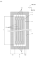
本発明の粘着シート付き配線回路基板の第1実施形態を図1~図4Bを参照して順に説明する。なお、図1において、導体層9(後述)の形状を明瞭に示すために、カバー絶縁層10(後述)を省略している。また、配線回路基板3(後述)および補強基板4(後述)の相対配置を明確に示すために、補強導体層14(後述)は、省略している。 A first embodiment of the wiring circuit board with adhesive sheet of the present invention will be described in order with reference to Figures 1 to 4B. In Figure 1, the cover insulating layer 10 (described later) is omitted in order to clearly show the shape of the conductor layer 9 (described later). Also, the reinforcing conductor layer 14 (described later) is omitted in order to clearly show the relative positioning of the wiring circuit board 3 (described later) and the reinforcing substrate 4 (described later).
図1および図2Eに示すように、この粘着シート付き配線回路基板1は、所定厚みを有し、厚み方向に直交する面方向に延びる略シート形状(板形状を含む)を有する。具体的には、粘着シート付き配線回路基板1は、面方向に含まれる第1方向の長さが長く、面方向に含まれ、第1方向に直交する第2方向の長さが短い平面視略矩形状を有する。
As shown in Figures 1 and 2E, this wired
粘着シート付き配線回路基板1は、粘着シート2と、配線回路基板3と、補強基板4とを備える。
The wired
粘着シート2は、所定厚みを有し、粘着シート付き配線回路基板1と同一の平面視形状を有する。また、粘着シート2は、可撓性を有しており、これにより、配線回路基板3および補強基板4とともに巻回されていてもよい。粘着シート2は、平面視において、配線回路基板3および補強基板4を含む。粘着シート2は、面方向に連続する。粘着シート2は、例えば、支持基材(図示せず)とその厚み方向一方面に配置される粘着剤層(図示せず)とを有する。支持基材としては、例えば、金属、樹脂などが挙げられる。粘着剤層としては、公知の粘着剤(感圧接着剤)から薄層に形成されている。これにより、粘着シート2の少なくとも厚み方向一方面は、粘着性(微タック)を有する。粘着シート2の厚みは、特に限定されず、例えば、10μm以上、好ましくは、20μm以上であり、また、例えば、200μm以下、好ましくは、150μm以下である。
The
粘着シート2の25℃におけるポリイミド板に対する粘着力(90度剥離接着力)は、例えば、0.05(N/20mm)以上、好ましくは、0.1(N/20mm)以上であり、また、例えば、1(N/20mm)以下、好ましくは、0.5(N/20mm)以下である。粘着シート2の粘着力が上記した下限以上であれば、粘着シート2が配線回路基板3および補強基板4を確実に粘着できる。粘着シート2の粘着力が上記した上限以下であれば、配線回路基板3を粘着シート2から容易に剥離できる。
The adhesive strength (90-degree peel adhesion) of the
配線回路基板3は、可撓性を有する。配線回路基板3は、平面視において、粘着シート2に包含される。具体的には、配線回路基板3は、平面視において、粘着シート2の第1方向中間部および第2方向中間部に配置されている。配線回路基板3は、所定厚みを有し、第1方向の長さが長く、第2方向の長さが短い平面視略矩形状を有する。配線回路基板3は、第1方向両端面、および第2方向両端面を有しており、これら端面は、具体的には、上記した切片(切れ端)を含まず、平坦である。
The
配線回路基板3の厚み方向他方面は、粘着シート2の厚み方向一方面に接触する。具体的には、配線回路基板3の厚み方向他方面は、粘着シート2の厚み方向一方面に粘着(接触)する。換言すれば、粘着シート2は、配線回路基板3の厚み方向他方面(他方側の面)に配置される。
The other thickness-wise surface of the
配線回路基板3の寸法は、特に限定されず、配線回路基板3の長さ(第1方向の長さ)Lが、例えば、30mm以上、好ましくは、300mm以上、より好ましくは、600mm以上、さらに好ましくは、800mm以上、とりわけ好ましくは、1,000mm以上であり、また、例えば、6,000mm以下、好ましくは、4,000mm以下である。配線回路基板3の長さLが上記した下限以上であれば、長尺の電子機器に実装できる。
The dimensions of the wired
配線回路基板3の幅(第2方向の長さ)Wは、例えば、50mm以下、好ましくは、25mm以下、より好ましくは、15mm以下であり、また、例えば、0.01mm以上である。配線回路基板3における長さ(第1方向の長さ)Lに対する幅(第2方向の長さ)Wの比(W/L)は、例えば、0.03以下、好ましくは、0.01以下、より好ましくは、0.005以下であり、また、例えば、0.00002以上である。幅Wが上記した上限以下であれば、狭小な領域に配線回路基板3を配置できる。幅の比(W/L)が上記した上限以下であれば、長尺な電子機器であり、かつ、狭小な内部に配線回路基板3を実装できる。
The width (length in the second direction) W of the
配線回路基板3は、ベース絶縁層8と、導体層9と、カバー絶縁層10とを備える。配線回路基板3は、好ましくは、光導波路を備えず、ベース絶縁層8と、導体層9と、カバー絶縁層10とのみを備える。
The
ベース絶縁層8は、配線回路基板3と同一の平面視形状を有する。ベース絶縁層8は、配線回路基板3の厚み方向他方面を形成する。ベース絶縁層8の材料としては、例えば、ポリイミドなどの、絶縁性を有する樹脂が挙げられる。ベース絶縁層8の厚みは、例えば、3μm以上、50μm以下である。
The
導体層9は、ベース絶縁層8の厚み方向一方面に配置されている。導体層9は、第1方向に延びる複数の配線11と、複数の配線11の第1方向両端部に連続する複数の端子12とを一体的に備える。導体層9の材料としては、例えば、銅などの導体が挙げられる。導体層9の厚みは、例えば、5μm以上、100μm以下である。
The
カバー絶縁層10は、ベース絶縁層8の厚み方向一方面に、配線11を被覆し、端子12を露出するように、配置されている。なお、カバー絶縁層10において、配線11を被覆する部分は、配線回路基板3の厚み方向一方面を形成する。カバー絶縁層10の材料としては、例えば、ポリイミドなどの、絶縁性を有する樹脂が挙げられる。カバー絶縁層10の厚みは、例えば、1μm以上、30μm以下である。
The
補強基板4は、平面視において、粘着シート2に包含されており、配線回路基板3の周囲に、配線回路基板3と間隔を隔てて配置されている。また、補強基板4は、配線回路基板3の周方向に沿って連続しており、具体的には、平面視略矩形枠形状を有する。粘着シート2は、配線回路基板3の厚み方向他方面と同じ側である補強基板4の厚み方向他方面に配置されている。要するに、補強基板4の厚み方向他方面は、粘着シート2の厚み方向一方面に粘着(接触)する。
The reinforcing
補強基板4は、補強ベース層13と、補強導体層14と、補強カバー層15とを備える。補強ベース層13と補強導体層14と補強カバー層15とのそれぞれは、配線回路基板3の上記したベース絶縁層8と導体層9とカバー絶縁層10とのそれぞれと同一層として形成されている。
The reinforcing
具体的には、補強ベース層13は、補強基板4の厚み方向他方面を形成する。補強ベース層13は、補強基板4と同一の平面視形状を有する。補強ベース層13の材料および厚みは、ベース絶縁層8のそれらと同一である。
Specifically, the reinforcing
補強導体層14は、平面視において補強ベース層13に含まれる。具体的には、補強導体層14は、平面視において、補強ベース層13より幅狭の帯形状を有する。補強導体層14は、補強ベース層13の厚み方向一方面に配置されている。補強導体層14の材料および厚みは、導体層9のそれらと同一である。
The reinforcing
補強カバー層15は、補強導体層14の厚み方向一方面および側面と、補強ベース層13の厚み方向一方面において補強導体層14と重ならない部分とに配置されている。補強カバー層15は、補強基板4の厚み方向一方面を形成する。補強カバー層15の材料および厚みは、カバー絶縁層10のそれらと同一である。
The reinforcing
補強基板4の幅W1は、補強基板4の内周面と外周面との距離であって、具体的には、例えば、0.1mm以上、好ましくは、0.5mm以上であり、また、例えば、50mm以下、好ましくは、30mm以下である。
The width W1 of the reinforcing
粘着シート2において、平面視において、配線回路基板3および補強基板4の間の領域は、隔離領域5として区画される。隔離領域5は、配線回路基板3と補強基板4とを隔てる。隔離領域5には、配線回路基板3および補強基板4が配置されていない。この隔離領域5には、配線回路基板3の外周面と、補強基板4の内周面とが臨む。また、隔離領域5からは、これに対応する粘着シート2の厚み方向一方面が厚み方向一方側に露出する。
In the
隔離領域5の幅W2は、配線回路基板3の外周面と、補強基板4の内周面との距離であって、具体的には、例えば、10μm以上、好ましくは、20μm以上であり、また、例えば、2000μm以下、好ましくは、1000μm以下である。隔離領域5の幅W2が上記した下限以上であれば、配線回路基板3を粘着シート2から円滑に剥離できる。隔離領域5の幅W2が上記した上限以下であれば、配線回路基板3を粘着シート2から剥離するときに、粘着シート2を確実に補強できる。
The width W2 of the
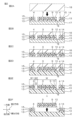
次に、第1実施形態の粘着シート付き配線回路基板1の製造方法を説明する。この方法は、第1工程~第5工程(図2A~図2E参照)を備える。この方法では、第1工程~第5工程が順に実施される。
[第1工程]
第1工程では、図2Aに示すように、支持シート17の厚み方向一方面に、ベース絶縁層8と、導体層9と、カバー絶縁層10とを厚み方向一方側に向かって順に形成する。併せて、補強ベース層13と、補強導体層14と、補強カバー層15とを厚み方向一方側に向かって順に形成する。これによって、配線回路基板3と、補強基板4とを、支持シート17の厚み方向一方面に同時に製造する。
Next, a method for producing the wired
[First step]
2A, in the first step, a
まず、図3Aに示すように、支持シート17を準備する。支持シート17は、粘着シート2および配線回路基板3を厚み方向他方側から支持(確保)できるシートであれば、特に限定されず、例えば、靱性、可撓性、剛性などの有するシートが挙げられる。支持シート17としては、例えば、ステンレス板などの金属板、例えば、ポリイミドシートなどの樹脂シート(感光性樹脂シートを含む)(非粘着性シート)、例えば、紙などが挙げられる。支持シート17として、優れた靱性および優れた剛性を確保する観点から、好ましくは、金属シート、より好ましくは、ステンレスシートが挙げられる。また、支持シート17は、単層または複層(積層体)である。支持シート17の厚みは、特に限定されず、例えば、5μm以上、好ましくは、15μm以上であり、また、例えば、5,000μm以下、好ましくは、500μm以下である。
First, as shown in FIG. 3A, the
続いて、図3Bに示すように、感光性の樹脂のワニスを、支持シート17の厚み方向一方面に塗布し、フォトリソグラフィにより、ベース絶縁層8および補強ベース層13を同時に形成する。次いで、図3Cに示すように、導体層9および補強導体層14のそれぞれを、ベース絶縁層8および補強ベース層13のそれぞれの厚み方向一方面に、アディティブ法、サブトラクティブ法などにより、形成する。その後、感光性の樹脂のワニスを、導体層9および補強ベース層13の厚み方向一方面と、ベース絶縁層8において導体層9から露出する厚み方向一方面と、補強ベース層13において補強導体層14から露出する厚み方向一方面と、支持シート17においてベース絶縁層8および補強ベース層13から露出する厚み方向一方面とに塗布し、フォトリソグラフィにより、図2Aに示すように、カバー絶縁層10および補強カバー層15を同時に形成する。
Next, as shown in FIG. 3B, a photosensitive resin varnish is applied to one thickness direction surface of the
これにより、第1工程では、支持シート17の厚み方向一方面に、配線回路基板3および補強基板4を同時に形成する。
[第2工程]
第2工程では、図2Bに示すように、第2支持シート18を、配線回路基板3および補強基板4の厚み方向一方面に接触させる。
As a result, in the first step, the wired
[Second step]
In the second step, as shown in FIG. 2B,
図2Aに示すように、第2支持シート18は、配線回路基板3および補強基板4を厚み方向一方側から支持(確保)できるシートであれば、特に限定されず、例えば、支持シート17と同様のシート(板)が挙げられる。第2支持シート18としては、好ましくは、樹脂シートが挙げられ、より好ましくは、レジスト用の樹脂シート、さらに好ましくは、第5工程において第2支持シート18を簡単に除去する(図2F参照)観点から、感光性樹脂シート、とりわけ好ましくは、感光性ドライフィルムレジスト(具体的には、感光前の感光性ドライフィルムレジスト)が挙げられる。
2A, the
図2Bに示すように、第2支持シート18が柔軟で追従性を有する樹脂シートであれば、第2工程では、第2支持シート18が、配線回路基板3および補強基板4の周側面と、粘着シート2において配線回路基板3および補強基板4の周囲の厚み方向一方面とに接触する。
[第3工程]
第3工程では、図2Cに示すように、支持シート17を除去する。支持シート17を除去する方法としては、特に限定されず、例えば、剥離、エッチングなどが挙げられる。支持シート17を除去することにより、配線回路基板3の厚み方向他方面と、補強基板4の厚み方向他方面と、粘着シート2において配線回路基板3および配線回路基板3の周囲の厚み方向他方面とが、厚み方向他方側に露出する。配線回路基板3および補強基板4の厚み方向他方面と、粘着シート2の厚み方向他方面とは、例えば、面一である。
As shown in Figure 2B, if
[Third step]
In the third step, as shown in Fig. 2C, the
底面視で、配線回路基板3と、補強基板4とは、間隔が隔てられている。しかし、第2支持シート18がそれらを少なくとも厚み方向一方側から支持する。好ましくは、第2支持シート18は、配線回路基板3と補強基板4とを、面方向両側からも支持する。そのため、配線回路基板3と補強基板4とは、第2支持シート18から脱離しない。つまり、配線回路基板3と補強基板4とは、第2支持シート18によって保持される。
[第4工程]
第4工程では、図2Dに示すように、粘着シート2を、配線回路基板3、補強基板4および第2支持シート18の厚み方向他方面に粘着させる。粘着シート2の厚み方向一方面と、配線回路基板3、補強基板4および第2支持シート18の厚み方向他方面とを接触させる。
[第5工程]
第5工程では、図2Eに示すように、第2支持シート18を除去する。第2支持シート18を除去する方法として、剥離、エッチング(ウエットエッチングなど)などが挙げられる。
In bottom view, the wired
[Fourth step]
2D , the
[Fifth step]
2E, the
これにより、配線回路基板3と、補強基板4とを、粘着シート2の厚み方向一方面に支持された状態で得る。つまり、配線回路基板3と、補強基板4と、配線回路基板3および補強基板4の厚み方向他方面に配置される粘着シート2とを備える粘着シート付き配線回路基板1を製造する。
This results in the
なお、平面視において、配線回路基板3と、補強基板4とは、間隔が隔てられているが、粘着シート2が配線回路基板3および補強基板4を厚み方向他方側からまとめて支持するので、配線回路基板3と補強基板4とが、粘着シート2から脱離しない。
In addition, in a plan view, the
その後、図2Fに示すように、配線回路基板3を、粘着シート2から剥離する。剥離され具体的には、図2Fの矢印で示すように、配線回路基板3が粘着シート2に対して厚み方向一方側に移動する。
Then, as shown in FIG. 2F, the
配線回路基板3は、別の電子機器に実装される。電子機器としては、特に限定されず、好ましくは、カテーテルが挙げられる。
The
配線回路基板が実装されたカテーテルを図4A~図4Bを参照して説明する。カテーテル51は、配線回路基板3と、配線回路基板3の端子12と電気的に接続される電子部品52と、それらを収容するカテーテルチューブ53とを備える。カテーテルチューブ53は、長尺の筒形状を有する。好ましくは、カテーテルチューブ53は、円筒形状を有する。長尺方向に直交する方向に沿う断面視で、カテーテルチューブ53の重心を通過する線上にある2つの内面間の最大距離(好ましくは、内径)Dが、例えば、50mm以下、好ましくは、30mm以下、より好ましくは、20mm以下であり、また、例えば、1mm以上である。最大距離Dが上記した上限以下であれば、カテーテル51は、人体への負荷を低減できる。
A catheter equipped with a wiring circuit board will be described with reference to Figs. 4A and 4B. The
(第1実施形態の作用効果)
そして、この粘着シート付き配線回路基板1では、図2Fに示すように、配線回路基板3を粘着シート2から剥離するだけで、切片(切れ端)を有さない配線回路基板3を得ることができる。そのため、かかる配線回路基板3を狭小な領域に円滑に実装できる。
(Functions and Effects of the First Embodiment)
2F, the wired
しかるに、配線回路基板3が300mm以上の長さLを有し、かつ、上記した切片(切れ端)を有する場合、ジョイント部を介してシートで保持するときには、多くのジョイント部を設けることが不可避となるため上記した切片の数が増大し、そのため、上記した不具合が顕在する。
However, if the wired
しかし、この粘着シート付き配線回路基板1からは、上記した切片(切れ端)を有さない配線回路基板3を得ることができる。そのため、長い配線回路基板3であっても、これを狭小な領域に円滑に実装できる。
However, from this wired
また、この粘着シート付き配線回路基板1は、厚み方向に投影したときに、粘着シート2に含まれ、面方向に連続する補強基板4をさらに備える。そのため、補強基板4に対応する粘着シート2を補強できる。そのため、配線回路基板3を粘着シート2から円滑かつ確実に剥離できる。
In addition, when projected in the thickness direction, this wired
この粘着シート付き配線回路基板1では、補強基板4が補強導体層14を含むので、補強基板4に対応する粘着シート2をより一層補強でき、配線回路基板3を粘着シート2からより一層円滑かつ確実に剥離できる。
In this
粘着シート付き配線回路基板1の製造方法では、図2Aに示すように、支持シート17の厚み方向一方面に配線回路基板3を形成し、次いで、図2Bに示すように、第2支持シート18を、配線回路基板3の厚み方向一方面に接触させ、その後、図2Cに示すように、支持シート17を除去するという簡便な方法で、上記した切片(切れ端)を有さない配線回路基板3を得ることができる。
In the method for manufacturing the wired
さらに、図2Dに示すように、粘着シート2を、配線回路基板3の厚み方向他方面に粘着させ、その後、図2Eに示すように、第2支持シート18を除去する。そのため、配線回路基板3を粘着シート2から剥離すれば、上記した切片(切れ端)を有さない配線回路基板3を簡便に得ることができる。
Furthermore, as shown in FIG. 2D, the
しかるに、配線回路基板3が300mm以上の長さLを有する場合には、上記した切片の数が増大し、そのため、切片を切断する手間が顕著に増大する。
However, if the wired
しかし、この粘着シート付き配線回路基板1の製造方法では、上記した切片(切れ端)を有さない配線回路基板3を得るため、たとえ、配線回路基板3が300mm以上の長さLを有する場合であっても、これを粘着シート2から剥離するという簡便な方法で、配線回路基板3を粘着シート2から分離して製造できる。
However, in this method for producing a wired
この方法の第2工程では、図2Bに示すように、第2支持シート18を、補強基板4の一方面に接触させるので、その後、図2Cに示すように、図3工程において、支持シート17を除去しても、補強基板4によって配線回路基板3の周囲が補強された第2支持シート18が、配線回路基板3を確実に支持できる。
In the second step of this method, as shown in FIG. 2B, the
この方法では、図2Bに示す第2工程において、第2支持シート18は、柔軟で追従性を有すれば、配線回路基板3の両側面を被覆するので、カバー絶縁層10から露出する端子12(図2Bにおいて図示せず)の周側面も被覆できる。そのため、図2Cに示す第3工程で、剥離液やエッチング液を用いるときでも、端子12の周側面を剥離液やエッチング液から保護できる。そのため、この配線回路基板3は、信頼性に優れる。
In this method, in the second step shown in FIG. 2B, if the
<変形例>
以下の各変形例において、上記した第1実施形態と同様の部材および工程については、同一の参照符号を付し、その詳細な説明を省略する。また、各変形例は、特記する以外、第1実施形態と同様の作用効果を奏することができる。さらに、第1実施形態およびその変形例を適宜組み合わせることができる。
<Modification>
In the following modifications, the same components and steps as those in the first embodiment are denoted by the same reference numerals, and detailed description thereof will be omitted. Each modification can achieve the same effects as those in the first embodiment, unless otherwise specified. Furthermore, the first embodiment and its modifications can be appropriately combined.
図5A~図5Bに示すように、補強導体層14が、平面視略格子形状を有する。そのため、材料コストを低減できながら、この補強基板4に対応する粘着シート2を均一に補強できる。
As shown in Figures 5A and 5B, the reinforcing
なお、補強導体層14の平面視形状は、上記に限定されず、例えば、図示しないが、ハニカム形状、三角形状、ドット形状などが挙げられる。
The planar shape of the reinforcing
粘着シート付き配線回路基板1は、1つの配線回路基板3を備えるが、例えば、図6に示すように、複数の配線回路基板3を備えることができる。
The adhesive sheet-attached
図6に示すように、複数の配線回路基板3は、第1方向および第2方向に間隔が隔てられる。補強基板4は、複数の配線回路基板3のそれぞれの周囲に連続して配置される。補強基板4は、具体的には、平面視略格子形状を有する。
As shown in FIG. 6, the multiple
第1実施形態の第3工程では、図2Cに示すように、支持シート17の全部を除去する。変形例では、図示しないが、支持シート17において配線回路基板3に対応する部分のみを除去する。詳しくは、この変形例では、支持シート17において、補強基板4および隔離領域5に対応する部分を残し、配線回路基板3に対応する部分を除去する。つまり、本発明では、第3工程において、支持シート17において少なくとも配線回路基板3に対応する部分を除去すればよい。
In the third step of the first embodiment, as shown in FIG. 2C, the
補強基板4は、補強ベース層13、補強導体層14および補強カバー層15を備えるが、3層のうちいずれか1層のみでもよく、また、いずれか2層であってもよい。好ましくは、少なくとも補強導体層14を含む1層~3層である。具体的には、補強基板4として、補強導体層14のみである1層、補強導体層14および補強ベース層13の2層、補強導体層14および補強カバー層15の2層、補強ベース層13、補強導体層14および補強カバー層15の3層が挙げられる。補強基板4が少なくとも補強導体層14を備えれば、補強基板4に対応する粘着シート2をより一層補強でき、配線回路基板3を粘着シート2からより一層円滑かつ確実に剥離できる。
The reinforcing
また、図示しないが、粘着シート付き配線回路基板1は、補強基板4を備えなくてもよい。好ましくは、第1実施形態のように、粘着シート付き配線回路基板1が補強基板4を備える。第1実施形態であれば、補強基板4に対応する粘着シート2を補強できる。そのため、配線回路基板3を粘着シート2から円滑かつ確実に剥離できる。
[第2実施形態]
第2実施形態において、上記した第1実施形態およびその変形例と同様の部材および工程については、同一の参照符号を付し、その詳細な説明を省略する。また、第2実施形態は、特記する以外、第1実施形態およびその変形例と同様の作用効果を奏することができる。さらに、第1実施形態、その変形例および第2実施形態を適宜組み合わせることができる。
Although not shown, the wired
[Second embodiment]
In the second embodiment, the same reference numerals are used for the same components and steps as those in the first embodiment and its modified examples, and detailed descriptions thereof will be omitted. In addition, the second embodiment can achieve the same effects as those in the first embodiment and its modified examples, unless otherwise specified. Furthermore, the first embodiment, its modified examples, and the second embodiment can be appropriately combined.
第2実施形態では、図7A~図7Bに示すように、第2支持シート18として粘着シート2を用い、第1工程~第3工程を順に実施する一方、第1実施形態の第4工程~第5工程を実施しない。
[第1工程]
第1工程では、図2Aに示すように、第2実施形態でも、第1実施形態と同様に、第1工程では、支持シート17の厚み方向一方面に、ベース絶縁層8と、導体層9と、カバー絶縁層10とを厚み方向一方側に向かって順に形成する。併せて、支持シート17の厚み方向一方面に、補強ベース層13と、補強導体層14と、補強カバー層15とを厚み方向一方側に向かって順に形成する。これによって、配線回路基板3および補強基板4を同時に、支持シート17の厚み方向一方面に製作する。
[第2工程]
第2工程では、図7Aの矢印で示すように、粘着シート2を、配線回路基板3および補強基板4の厚み方向一方面に接触させる。具体的には、粘着シート2の厚み方向他方面を、配線回路基板3および補強基板4の厚み方向一方面に粘着させる。
[第3工程]
第3工程では、図7Bに示すように、支持シート17を除去する。
In the second embodiment, as shown in Figures 7A to 7B, an
[First step]
2A, in the second embodiment, as in the first embodiment, in the first step, a
[Second step]
7A , the
[Third step]
In the third step, as shown in FIG. 7B, the
これにより、配線回路基板3と、補強基板4と、配線回路基板3および補強基板4の厚み方向一方面が配置される粘着シート2とを備える。
This results in a
その後、図7Cに示すように、配線回路基板3を、粘着シート2から剥離する。具体的には、図7Cの矢印で示すように、配線回路基板3が粘着シート2に対して厚み方向他方側に移動する。
Then, as shown in FIG. 7C, the
(第2実施形態の作用効果)
第2実施形態は、図7Aに示すように、粘着シート2を、配線回路基板3の厚み方向他方面に粘着させ、その後、図7Bに示すように、支持シート17を除去する。そのため、配線回路基板3を粘着シート2から離間させれば、上記した切片(切れ端)を有さない配線回路基板3を簡便に得ることができる。また、第4工程および第5工程を実施しないため、工数を低減できる。さらに、第2支持シート18を用いないため、製造コストを低減できる。
(Functions and Effects of the Second Embodiment)
In the second embodiment, as shown in Fig. 7A, the
一方、第2実施形態は、図7Bに示すように、粘着シート2が配線回路基板3の厚み方向一方面に粘着している。そのため、配線回路基板3を粘着シート2から剥離する際、端子12(図7Bにおいて図示せず)の厚み方向一方面に糊残りし、そのため、端子12における電気的な接続信頼性が低下する場合がある。他方、第1実施形態では、図2Eに示すように、粘着シート2が配線回路基板3の厚み方向他方面に粘着している。そのため、配線回路基板3を粘着シート2から剥離する際、ベース絶縁層8の厚み方向他方面に糊残りしても、端子12(図2Eにおいて図示せず)における上記した接続信頼性の低下を抑制できる。
[第3実施形態]
第3実施形態において、上記した第1実施形態、その変形例および第2実施形態と同様の部材および工程については、同一の参照符号を付し、その詳細な説明を省略する。また、第3実施形態は、特記する以外、第1実施形態、その変形例および第2実施形態と同様の作用効果を奏することができる。さらに、第1実施形態、その変形例、第2実施形態および第3実施形態を適宜組み合わせることができる。
On the other hand, in the second embodiment, as shown in Fig. 7B, the
[Third embodiment]
In the third embodiment, the same reference numerals are used for the same members and steps as those in the first embodiment, its modified example, and the second embodiment, and detailed description thereof will be omitted. In addition, the third embodiment can achieve the same effects as those in the first embodiment, its modified example, and the second embodiment, unless otherwise specified. Furthermore, the first embodiment, its modified example, the second embodiment, and the third embodiment can be appropriately combined.
図9Hに示すように、配線回路基板3は、金属支持層20をさらに備える金属支持層付き配線回路基板である。この配線回路基板3は、金属支持層20と、ベース絶縁層8と、導体層9と、カバー絶縁層10とを備える。配線回路基板3は、好ましくは、光導波路を備えず、金属支持層20と、ベース絶縁層8と、導体層9と、カバー絶縁層10とのみを備える。
As shown in FIG. 9H, the
金属支持層20は、ベース絶縁層8の厚み方向他方面に配置されている。金属支持層20は、底面視において、ベース絶縁層8に含まれており、ベース絶縁層8より小さい。そのため、金属支持層20は、ベース絶縁層8の厚み方向他方面の周端部を露出する。金属支持層20は、配線回路基板3の厚み方向他方面を形成する。金属支持層20の材料としては、例えば、金属が挙げられ、好ましくは、優れた靱性を確保する観点から、ステンレスが挙げられる。金属支持層20の厚みは、例えば、5μm以上、100μm以下である。
The
補強基板4は、補強金属支持層26をさらに備える。補強基板4は、補強金属支持層26と、補強ベース層13と、補強導体層14と、補強カバー層15とを備える。
The reinforcing
補強金属支持層26は、平面視において、補強ベース層13に含まれる。補強金属支持層26は、補強基板4の厚み方向他方面を形成する。補強金属支持層26において金属支持層20に面する内端面は、厚み方向に投影したときに、補強ベース層13においてベース絶縁層8に面する内端面より、外側に配置される。補強金属支持層26は、金属支持層20と同一層として形成されている。
The reinforcing
金属支持層20および補強金属支持層26を備える粘着シート付き配線回路基板1の製造方法を図2Aおよび図8A~図9Hを参照して説明する。
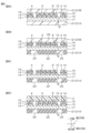
A method for manufacturing a
この方法では、第1工程~第3工程を順に実施する。
[第1工程]
第1工程では、図2Aに示すように、第1実施形態の第1工程と同様に、支持シート17の厚み方向一方面に、ベース絶縁層8と、導体層9と、カバー絶縁層10とを厚み方向一方側に向かって順に形成する。同時に、支持シート17の厚み方向一方面に、補強ベース層13と、補強導体層14と、補強カバー層15とを厚み方向一方側に向かって順に形成する。これによって、配線回路基板3と、補強基板4とを、支持シート17の厚み方向一方面に製造する。
In this method, the first to third steps are carried out in this order.
[First step]
2A, in the first step, similarly to the first step of the first embodiment, a
第1工程では、支持シート17は、好ましくは、金属板であり、より好ましくは、ステンレス板である。支持シート17は、金属支持層20および補強金属支持層26を形成するための金属シートである。
[第2工程]
第2工程では、図8Dに示すように、第2実施形態の第2工程と同様に、粘着シート2を、配線回路基板3および補強基板4の厚み方向一方面に接触させる。
[第3工程]
第3工程では、図9Eに示すように、支持シート17において配線回路基板3の周囲の部分を除去する。これにより、支持シート17の隔離領域5が厚み方向他方側に向かって露出する。例えば、エッチングレジスト24(図8A参照)を用いて、支持シート17をエッチングする。エッチングレジスト24は、金属支持層20および補強金属支持層26と同一パターンを有する。エッチングレジスト24は、フォトレジスト21をフォトリソグラフィすることによって形成される。
In the first step, the
[Second step]
In the second step, as shown in FIG. 8D, the
[Third step]
In the third step, as shown in Fig. 9E, the portion of the
エッチングレジスト24を形成するには、例えば、まず、図8Aに示すように、第1工程の後であって、第2工程の前に、2つのフォトレジスト21のそれぞれを、支持シート17と、配線回路基板3および補強基板4とのそれぞれに配置する。具体的には、第1フォトレジスト21Aを、支持シート17の厚み方向他方面に配置する。第2フォトレジスト21Bを、配線回路基板3および補強基板4の厚み方向一方面に配置する。
To form the etching resist 24, for example, first, as shown in FIG. 8A, after the first step and before the second step, two
その後、図8Bに示すように、フォトリソグラフィによって、第1フォトレジスト21Aを図示しないフォトマスクを介して露光して、残存予定部分22および除去予定部分23からなる潜像を形成する。一方、第2フォトレジスト21Bは、露光しない。そのため、第2フォトレジスト21Bは、除去予定部分23となる。なお、フォトレジスト21がネガ型であれば、残存予定部分22が露光部分であり、除去予定部分23が未露光部分である。
Then, as shown in FIG. 8B, the
続いて、図8Cに示すように、第2フォトレジスト21Bのみを現像により除去する。具体的には、第1フォトレジスト21Aを現像せずに残し、第2フォトレジスト21Bを現像により除去する。その後、第3工程において、図8Dに示すように、第2フォトレジスト21Bが配置されていた、配線回路基板3および補強基板4の厚み方向一方面に、粘着シート2を配置する。
Next, as shown in FIG. 8C, only the
第3工程の後、図9Eに示すように、第1フォトレジスト21Aを現像して、エッチングレジスト24を形成する。第1フォトレジスト21Aの現像では、除去予定部分23が除去され、残存予定部分22が残存してエッチングレジスト24となる。
After the third step, as shown in FIG. 9E, the
その後、図9Fに示すように、エッチングレジスト24から露出する支持シート17をエッチングして、金属支持層20および補強金属支持層26を形成する。
Then, as shown in FIG. 9F, the
これにより、配線回路基板3と、補強基板4とを、粘着シート2の厚み方向他方面に支持された状態で得る。つまり、配線回路基板3および補強基板4と、それらの厚み方向一方面に配置される粘着シート2とを備える粘着シート付き配線回路基板1を製造する。
This results in the
その後、図9Hの矢印で示すように、配線回路基板3を粘着シート2に対して厚み方向他方側に移動させることにより、配線回路基板3を粘着シート2から剥離する。
Then, as shown by the arrow in Figure 9H, the
(第3実施形態の作用効果)
この粘着シート付き配線回路基板1およびその製造方法では、配線回路基板3が金属支持層20をさらに備えるので、靱性に優れる配線回路基板3を得ることができる。
(Operation and effect of the third embodiment)
In this wired
また、この方法では、図9Fに示すように、支持シート17において配線回路基板3の周囲の部分を除去するので、配線回路基板3を、支持シート17においてその部分の外側部分から確実に分離できる。
[第4実施形態]
第4実施形態において、上記した第1実施形態、その変形例、第2実施形態および第3実施形態と同様の部材および工程については、同一の参照符号を付し、その詳細な説明を省略する。また、第1実施形態、その変形例、第2実施形態および第3実施形態は、特記する以外、第1実施形態、その変形例、第2実施形態および第3実施形態と同様の作用効果を奏することができる。さらに、第1実施形態、その変形例、第2実施形態~第4実施形態を適宜組み合わせることができる。
In addition, in this method, as shown in FIG. 9F, the portion of
[Fourth embodiment]
In the fourth embodiment, the same components and steps as those in the first embodiment, its modified example, the second embodiment, and the third embodiment described above are denoted by the same reference numerals, and detailed description thereof will be omitted. Furthermore, the first embodiment, its modified example, the second embodiment, and the third embodiment can achieve the same effects as those of the first embodiment, its modified example, the second embodiment, and the third embodiment, unless otherwise specified. Furthermore, the first embodiment, its modified example, and the second to fourth embodiments can be appropriately combined.
第4実施形態では、第3実施形態で製造し、図9Gに示す配線回路基板3を、補強基板4とともに、図10A~図10Bに示すように、第2粘着シート25に転写する(第6工程)。
In the fourth embodiment, the
具体的には、図10Aに示すように、第2粘着シート25を、配線回路基板3および補強基板4の厚み方向他方面に接触(粘着)させる。第2粘着シート25は、粘着シート2と同様の構成を有する。但し、第2粘着シート25の粘着力は、粘着シート2の粘着力より大きい。
Specifically, as shown in FIG. 10A, the
その後、図10Bに示すように、粘着シート2を、配線回路基板3および補強基板4の厚み方向一方面から剥離する。
Then, as shown in FIG. 10B, the
これにより、配線回路基板3と、補強基板4とを、第2粘着シート25の厚み方向一方面に支持された状態で得る。つまり、配線回路基板3および補強基板4と、それらの厚み方向他方面に配置される第2粘着シート25とを備える粘着シート付き配線回路基板1を製造する。
This results in the
図10Bの仮想線および矢印で示すように、配線回路基板3を第2粘着シート25に対して厚み方向一方側に移動させることにより、配線回路基板3を第2粘着シート25から剥離する。
As shown by the imaginary lines and arrows in FIG. 10B, the
(第4実施形態の作用効果)
そして、この方法では、第6工程で、配線回路基板3を、粘着シート2から第2粘着シート25に転写するので、図10Bの仮想線および矢印で示すように、配線回路基板3を第2粘着シート25から離間させれば、上記した切片(切れ端)を有さない配線回路基板3を簡便に得ることができる。
(Functions and Effects of the Fourth Embodiment)
In this method, in the sixth step, the wired
第3実施形態では、図9Gに示すように、配線回路基板3(カバー絶縁層10)粘着シート2の厚み方向他方面に粘着させ、その後、配線回路基板3を厚み方向他方側に移動させて、配線回路基板3を得る。対して、第4実施形態では、配線回路基板3(金属支持層20)を粘着シート2の厚み方向一方面に粘着させ、その後、配線回路基板3を厚み方向一方側に移動させて、配線回路基板3を得る。従って、配線回路基板3を粘着シート2の厚み方向一方面および他方面のいずれの面に粘着させるか、または、配線回路基板3を厚み方向一方側および他方側のいずれの方向に移動させるかを、配線回路基板3の使用状況に応じて、第3また第4実施形態を適宜選択する。
In the third embodiment, as shown in FIG. 9G, the wiring circuit board 3 (cover insulating layer 10) is adhered to the other thickness-wise surface of the
1 粘着シート付き配線回路基板
2 粘着シート
3 配線回路基板
4 補強基板
7 補強基板
8 ベース絶縁層
9 導体層
10 カバー絶縁層
14 補強導体層
17 支持シート
18 第2支持シート
20 金属支持層
25 第2粘着シート
L 長さ(配線回路基板)
Claims (11)
前記配線回路基板の前記厚み方向に直交する面方向において、前記配線回路基板の全外周面と間隔を隔てて囲む補強基板と、
前記配線回路基板の厚み方向一方側および他方側のいずれかの面に配置される粘着シートと
を備え、
前記粘着シートは、前記厚み方向に投影したときに、前記配線回路基板および前記補強基板を含み、前記面方向に連続しており、前記配線回路基板の厚み方向一方側および他方側のいずれかの前記面と同じ側の前記補強基板の面に配置され、
前記配線回路基板の外周面と前記補強基板の内周面との距離である隔離領域の幅は、10μm以上、2000μm以下であり、
前記補強基板は、補強導体層を含むことを特徴とする、粘着シート付き配線回路基板。 a wired circuit board including a base insulating layer, a conductor layer disposed on one surface in a thickness direction of the base insulating layer, and a cover insulating layer disposed on the one surface in the thickness direction of the base insulating layer so as to cover the conductor layer;
a reinforcing substrate surrounding the entire outer peripheral surface of the wiring circuit board at a distance in a plane direction perpendicular to the thickness direction of the wiring circuit board;
an adhesive sheet disposed on either one surface or the other surface of the wiring circuit board in a thickness direction;
the pressure-sensitive adhesive sheet includes the wiring circuit board and the reinforcing substrate when projected in the thickness direction, is continuous in the plane direction, and is disposed on a surface of the reinforcing substrate on the same side as one of the surfaces on one and the other sides in the thickness direction of the wiring circuit board;
a width of an isolation region, which is a distance between an outer peripheral surface of the wired circuit board and an inner peripheral surface of the reinforcing substrate, is 10 μm or more and 2000 μm or less;
The reinforcing substrate includes a reinforcing conductor layer .
着シート付き配線回路基板。 The wired circuit board with an adhesive sheet according to claim 1 , wherein the reinforcing conductor layer has a generally lattice shape in a plan view.
第2支持シートを、前記配線回路基板の前記厚み方向一方面に接触させ、前記第2支持シートを、前記補強基板の厚み方向一方面に接触させる第2工程と、
前記支持シートにおいて前記配線回路基板に対応する部分を除去する第3工程と
を備え、
前記補強基板は、補強導体層を含むことを特徴とする、粘着シート付き配線回路基板の製造方法。 a first step of forming a base insulating layer, a conductor layer, and a cover insulating layer in this order toward one side in the thickness direction on one surface of a support sheet in the thickness direction to form a wiring circuit board on the one surface of the support sheet in the thickness direction, and forming a reinforcing substrate on the one surface of the support sheet in the thickness direction so as to surround the entire outer periphery of the wiring circuit board at a distance therefrom;
a second step of contacting a second support sheet with one surface in the thickness direction of the wired circuit board and contacting the second support sheet with one surface in the thickness direction of the reinforcing substrate;
a third step of removing a portion of the support sheet corresponding to the wired circuit board,
2. A method for producing a wired circuit board with an adhesive sheet, wherein the reinforcing substrate includes a reinforcing conductor layer .
前記第3工程の後に、粘着シートを、前記配線回路基板の前記厚み方向他方面に粘着させる第4工程と、
前記第4工程の後に、前記第2支持シートを除去する第5工程と
をさらに備えることを特徴とする、請求項5に記載の粘着シート付き配線回路基板の製造方法。 In the third step, the support sheet is removed,
a fourth step of adhering an adhesive sheet to the other surface in the thickness direction of the wired circuit board after the third step;
6. The method for producing a wired circuit board with an adhesive sheet according to claim 5 , further comprising a fifth step of removing the second support sheet after the fourth step.
備えることを特徴とする、請求項6に記載の粘着シート付き配線回路基板の製造方法。The method for producing a wired circuit board with an adhesive sheet according to claim 6, further comprising:
前記第3工程では、前記金属シートから、前記ベース絶縁層の厚み方向他方面に配置される金属支持層を形成することを特徴とする、請求項8に記載の粘着シート付き配線回路基板の製造方法。 The support sheet is a metal sheet,
9. The method for producing a wired circuit board with an adhesive sheet according to claim 8 , wherein in the third step, a metal support layer is formed from the metal sheet, the metal support layer being disposed on the other surface in the thickness direction of the base insulating layer.
Priority Applications (4)
| Application Number | Priority Date | Filing Date | Title |
|---|---|---|---|
| JP2019193054A JP7609552B2 (en) | 2019-10-23 | 2019-10-23 | Wired circuit board with adhesive sheet and method for producing same |
| US17/075,061 US12144125B2 (en) | 2019-10-23 | 2020-10-20 | Pressure-sensitive adhesive sheet-including wiring circuit board and producing method thereof |
| CN202011141450.4A CN112702832A (en) | 2019-10-23 | 2020-10-22 | Adhesive sheet-attached wiring circuit board and method for manufacturing same |
| JP2024123040A JP2024138155A (en) | 2019-10-23 | 2024-07-30 | Wired circuit board with adhesive sheet and method for producing same |
Applications Claiming Priority (1)
| Application Number | Priority Date | Filing Date | Title |
|---|---|---|---|
| JP2019193054A JP7609552B2 (en) | 2019-10-23 | 2019-10-23 | Wired circuit board with adhesive sheet and method for producing same |
Related Child Applications (1)
| Application Number | Title | Priority Date | Filing Date |
|---|---|---|---|
| JP2024123040A Division JP2024138155A (en) | 2019-10-23 | 2024-07-30 | Wired circuit board with adhesive sheet and method for producing same |
Publications (2)
| Publication Number | Publication Date |
|---|---|
| JP2021068808A JP2021068808A (en) | 2021-04-30 |
| JP7609552B2 true JP7609552B2 (en) | 2025-01-07 |
Family
ID=75505851
Family Applications (2)
| Application Number | Title | Priority Date | Filing Date |
|---|---|---|---|
| JP2019193054A Active JP7609552B2 (en) | 2019-10-23 | 2019-10-23 | Wired circuit board with adhesive sheet and method for producing same |
| JP2024123040A Withdrawn JP2024138155A (en) | 2019-10-23 | 2024-07-30 | Wired circuit board with adhesive sheet and method for producing same |
Family Applications After (1)
| Application Number | Title | Priority Date | Filing Date |
|---|---|---|---|
| JP2024123040A Withdrawn JP2024138155A (en) | 2019-10-23 | 2024-07-30 | Wired circuit board with adhesive sheet and method for producing same |
Country Status (3)
| Country | Link |
|---|---|
| US (1) | US12144125B2 (en) |
| JP (2) | JP7609552B2 (en) |
| CN (1) | CN112702832A (en) |
Families Citing this family (1)
| Publication number | Priority date | Publication date | Assignee | Title |
|---|---|---|---|---|
| JP7790998B2 (en) * | 2022-02-04 | 2025-12-23 | 日東電工株式会社 | Wired circuit board and wired circuit board assembly |
Citations (4)
| Publication number | Priority date | Publication date | Assignee | Title |
|---|---|---|---|---|
| JP2008004631A (en) | 2006-06-20 | 2008-01-10 | Sharp Corp | Substrate base material for flexible printed wiring board and method for manufacturing flexible printed wiring board |
| JP2018166134A (en) | 2017-03-28 | 2018-10-25 | 日東電工株式会社 | Method for manufacturing suspension board assembly with circuit |
| JP2019068032A (en) | 2017-04-10 | 2019-04-25 | 日東電工株式会社 | Imaging sensor mounting substrate, method for manufacturing the same, and mounting substrate assembly |
| JP2019079996A (en) | 2017-10-26 | 2019-05-23 | 日東電工株式会社 | Substrate assembly sheet |
Family Cites Families (15)
| Publication number | Priority date | Publication date | Assignee | Title |
|---|---|---|---|---|
| JPH0638436Y2 (en) * | 1989-12-30 | 1994-10-05 | 日本メクトロン株式会社 | Flexible circuit board assembly |
| JP2654735B2 (en) * | 1992-12-04 | 1997-09-17 | 日東電工株式会社 | Label base material, ink and label |
| EP0675673A3 (en) * | 1994-03-30 | 1997-03-05 | Nitto Denko Corp | Reinforcement for flexible printed circuit board and reinforced flexible circuit board. |
| JP3512655B2 (en) * | 1998-12-01 | 2004-03-31 | シャープ株式会社 | Semiconductor device, method of manufacturing the same, and reinforcing tape used for manufacturing the semiconductor device |
| JP2004186324A (en) * | 2002-12-02 | 2004-07-02 | Sony Chem Corp | Manufacturing method of flexible printed circuit board |
| JP3751938B2 (en) * | 2002-12-09 | 2006-03-08 | 日東電工株式会社 | TAB tape carrier and method for manufacturing the same |
| JP2006203094A (en) * | 2005-01-24 | 2006-08-03 | Shin Etsu Polymer Co Ltd | Fixing tool for electronic component |
| JP4549939B2 (en) | 2005-06-28 | 2010-09-22 | 日東電工株式会社 | Wiring circuit board holding sheet |
| JP4753749B2 (en) | 2006-03-03 | 2011-08-24 | 日東電工株式会社 | Wiring circuit board assembly sheet and manufacturing method thereof |
| JP5175779B2 (en) * | 2008-04-18 | 2013-04-03 | 日東電工株式会社 | Method for manufacturing printed circuit board |
| JP4852137B2 (en) * | 2009-11-11 | 2012-01-11 | 日東電工株式会社 | Catheter and manufacturing method thereof |
| JP2012129472A (en) | 2010-12-17 | 2012-07-05 | Sumitomo Electric Printed Circuit Inc | Aggregate sheet of flexible printed wiring board |
| CN102842541A (en) * | 2011-06-22 | 2012-12-26 | 日东电工株式会社 | Laminated film and use thereof |
| KR20130059291A (en) * | 2011-11-28 | 2013-06-05 | 닛토덴코 가부시키가이샤 | Underfill material and method for manufacturing semiconductor device |
| KR102035378B1 (en) * | 2015-06-08 | 2019-11-18 | 주식회사 엘지화학 | A laminate structure with metal wiring layer and a process for manufacturing same |
-
2019
- 2019-10-23 JP JP2019193054A patent/JP7609552B2/en active Active
-
2020
- 2020-10-20 US US17/075,061 patent/US12144125B2/en active Active
- 2020-10-22 CN CN202011141450.4A patent/CN112702832A/en active Pending
-
2024
- 2024-07-30 JP JP2024123040A patent/JP2024138155A/en not_active Withdrawn
Patent Citations (4)
| Publication number | Priority date | Publication date | Assignee | Title |
|---|---|---|---|---|
| JP2008004631A (en) | 2006-06-20 | 2008-01-10 | Sharp Corp | Substrate base material for flexible printed wiring board and method for manufacturing flexible printed wiring board |
| JP2018166134A (en) | 2017-03-28 | 2018-10-25 | 日東電工株式会社 | Method for manufacturing suspension board assembly with circuit |
| JP2019068032A (en) | 2017-04-10 | 2019-04-25 | 日東電工株式会社 | Imaging sensor mounting substrate, method for manufacturing the same, and mounting substrate assembly |
| JP2019079996A (en) | 2017-10-26 | 2019-05-23 | 日東電工株式会社 | Substrate assembly sheet |
Also Published As
| Publication number | Publication date |
|---|---|
| JP2024138155A (en) | 2024-10-07 |
| US20210127499A1 (en) | 2021-04-29 |
| CN112702832A (en) | 2021-04-23 |
| US12144125B2 (en) | 2024-11-12 |
| JP2021068808A (en) | 2021-04-30 |
Similar Documents
| Publication | Publication Date | Title |
|---|---|---|
| US9955580B2 (en) | Method of manufacturing rigid-flexible printed circuit board | |
| US7649144B2 (en) | Connection structure between wired circuit boards | |
| US20090039053A1 (en) | Method for manufacturing electrical traces of printed circuit boards | |
| TWI640234B (en) | Circuit board with coppercircuit and method for manufacturing same | |
| EP1651016B1 (en) | Wired circuit board comprising terminals for connecting to external terminals through molten metal | |
| US20110318480A1 (en) | Method of manufacturing substrate using a carrier | |
| JP2024138155A (en) | Wired circuit board with adhesive sheet and method for producing same | |
| EP1635624A2 (en) | Wired circuit board | |
| JP5227753B2 (en) | Method for manufacturing printed circuit board | |
| JP5175779B2 (en) | Method for manufacturing printed circuit board | |
| US7452754B2 (en) | Method for manufacturing flexible printed circuit boards | |
| CN109429442B (en) | Circuit board and manufacturing method thereof | |
| TWI637666B (en) | Printed circuit board and mthod for manufacturing same | |
| KR20130132089A (en) | Printed circuit board and method for fabricating the same | |
| JP7481794B2 (en) | Roll body | |
| US12185479B2 (en) | Flexible circuit board and manufacturing method thereof | |
| TWI420990B (en) | Method for manufacturing printed circuit board | |
| US20240206053A1 (en) | Wiring circuit board and method for producing wiring circuit board | |
| JP2006202849A (en) | Manufacturing method of printed circuit board with reinforcing plate | |
| JP7555206B2 (en) | Manufacturing method for printed wiring board | |
| KR200345621Y1 (en) | Zebra connector with an flexible printed circuit board | |
| JP2501558B2 (en) | Manufacturing method of flexible wiring board | |
| KR100771308B1 (en) | Manufacturing method of rigid-flexible printed circuit board | |
| JP2024054433A (en) | Method for manufacturing wiring board and flexible printed wiring board | |
| JP2018182252A (en) | Manufacturing method of printed wiring board |
Legal Events
| Date | Code | Title | Description |
|---|---|---|---|
| A621 | Written request for application examination |
Free format text: JAPANESE INTERMEDIATE CODE: A621 Effective date: 20220922 |
|
| A977 | Report on retrieval |
Free format text: JAPANESE INTERMEDIATE CODE: A971007 Effective date: 20230726 |
|
| A131 | Notification of reasons for refusal |
Free format text: JAPANESE INTERMEDIATE CODE: A131 Effective date: 20230905 |
|
| A521 | Request for written amendment filed |
Free format text: JAPANESE INTERMEDIATE CODE: A523 Effective date: 20231102 |
|
| A131 | Notification of reasons for refusal |
Free format text: JAPANESE INTERMEDIATE CODE: A131 Effective date: 20240123 |
|
| A521 | Request for written amendment filed |
Free format text: JAPANESE INTERMEDIATE CODE: A523 Effective date: 20240322 |
|
| A02 | Decision of refusal |
Free format text: JAPANESE INTERMEDIATE CODE: A02 Effective date: 20240625 |
|
| A521 | Request for written amendment filed |
Free format text: JAPANESE INTERMEDIATE CODE: A523 Effective date: 20240730 |
|
| A911 | Transfer to examiner for re-examination before appeal (zenchi) |
Free format text: JAPANESE INTERMEDIATE CODE: A911 Effective date: 20240806 |
|
| TRDD | Decision of grant or rejection written | ||
| A01 | Written decision to grant a patent or to grant a registration (utility model) |
Free format text: JAPANESE INTERMEDIATE CODE: A01 Effective date: 20241126 |
|
| A61 | First payment of annual fees (during grant procedure) |
Free format text: JAPANESE INTERMEDIATE CODE: A61 Effective date: 20241219 |
|
| R150 | Certificate of patent or registration of utility model |
Ref document number: 7609552 Country of ref document: JP Free format text: JAPANESE INTERMEDIATE CODE: R150 |