JP7597464B2 - プラズマ処理装置 - Google Patents
プラズマ処理装置 Download PDFInfo
- Publication number
- JP7597464B2 JP7597464B2 JP2021020071A JP2021020071A JP7597464B2 JP 7597464 B2 JP7597464 B2 JP 7597464B2 JP 2021020071 A JP2021020071 A JP 2021020071A JP 2021020071 A JP2021020071 A JP 2021020071A JP 7597464 B2 JP7597464 B2 JP 7597464B2
- Authority
- JP
- Japan
- Prior art keywords
- conductive member
- plasma processing
- electrode
- conductive
- power source
- Prior art date
- Legal status (The legal status is an assumption and is not a legal conclusion. Google has not performed a legal analysis and makes no representation as to the accuracy of the status listed.)
- Active
Links
- 238000012545 processing Methods 0.000 title claims description 80
- 239000000758 substrate Substances 0.000 claims description 31
- 230000008859 change Effects 0.000 claims description 24
- 230000007246 mechanism Effects 0.000 claims description 8
- 229910001285 shape-memory alloy Inorganic materials 0.000 claims description 8
- 230000004044 response Effects 0.000 claims description 3
- 239000007789 gas Substances 0.000 description 39
- 239000012212 insulator Substances 0.000 description 7
- 239000004020 conductor Substances 0.000 description 6
- 230000004323 axial length Effects 0.000 description 5
- XAGFODPZIPBFFR-UHFFFAOYSA-N aluminium Chemical compound [Al] XAGFODPZIPBFFR-UHFFFAOYSA-N 0.000 description 4
- 229910052782 aluminium Inorganic materials 0.000 description 4
- 230000006870 function Effects 0.000 description 4
- 229910045601 alloy Inorganic materials 0.000 description 3
- 239000000956 alloy Substances 0.000 description 3
- 238000004891 communication Methods 0.000 description 3
- 238000009792 diffusion process Methods 0.000 description 3
- KHYBPSFKEHXSLX-UHFFFAOYSA-N iminotitanium Chemical compound [Ti]=N KHYBPSFKEHXSLX-UHFFFAOYSA-N 0.000 description 3
- 238000000034 method Methods 0.000 description 3
- 229910001000 nickel titanium Inorganic materials 0.000 description 3
- 230000008569 process Effects 0.000 description 3
- 238000012546 transfer Methods 0.000 description 3
- 238000010586 diagram Methods 0.000 description 2
- 230000001105 regulatory effect Effects 0.000 description 2
- 229910052710 silicon Inorganic materials 0.000 description 2
- 239000010703 silicon Substances 0.000 description 2
- PNEYBMLMFCGWSK-UHFFFAOYSA-N aluminium oxide Inorganic materials [O-2].[O-2].[O-2].[Al+3].[Al+3] PNEYBMLMFCGWSK-UHFFFAOYSA-N 0.000 description 1
- 238000005513 bias potential Methods 0.000 description 1
- 239000012267 brine Substances 0.000 description 1
- 238000005530 etching Methods 0.000 description 1
- 239000013529 heat transfer fluid Substances 0.000 description 1
- 238000012986 modification Methods 0.000 description 1
- 230000004048 modification Effects 0.000 description 1
- 239000012811 non-conductive material Substances 0.000 description 1
- HPALAKNZSZLMCH-UHFFFAOYSA-M sodium;chloride;hydrate Chemical compound O.[Na+].[Cl-] HPALAKNZSZLMCH-UHFFFAOYSA-M 0.000 description 1
- 239000007787 solid Substances 0.000 description 1
Images


Classifications
-
- H—ELECTRICITY
- H01—ELECTRIC ELEMENTS
- H01J—ELECTRIC DISCHARGE TUBES OR DISCHARGE LAMPS
- H01J37/00—Discharge tubes with provision for introducing objects or material to be exposed to the discharge, e.g. for the purpose of examination or processing thereof
- H01J37/32—Gas-filled discharge tubes
- H01J37/32431—Constructional details of the reactor
- H01J37/32532—Electrodes
- H01J37/3255—Material
-
- G—PHYSICS
- G05—CONTROLLING; REGULATING
- G05D—SYSTEMS FOR CONTROLLING OR REGULATING NON-ELECTRIC VARIABLES
- G05D3/00—Control of position or direction
-
- H—ELECTRICITY
- H01—ELECTRIC ELEMENTS
- H01J—ELECTRIC DISCHARGE TUBES OR DISCHARGE LAMPS
- H01J37/00—Discharge tubes with provision for introducing objects or material to be exposed to the discharge, e.g. for the purpose of examination or processing thereof
- H01J37/32—Gas-filled discharge tubes
- H01J37/32431—Constructional details of the reactor
- H01J37/32458—Vessel
- H01J37/32522—Temperature
-
- H—ELECTRICITY
- H01—ELECTRIC ELEMENTS
- H01J—ELECTRIC DISCHARGE TUBES OR DISCHARGE LAMPS
- H01J37/00—Discharge tubes with provision for introducing objects or material to be exposed to the discharge, e.g. for the purpose of examination or processing thereof
- H01J37/32—Gas-filled discharge tubes
- H01J37/32431—Constructional details of the reactor
- H01J37/32532—Electrodes
- H01J37/32568—Relative arrangement or disposition of electrodes; moving means
-
- H—ELECTRICITY
- H01—ELECTRIC ELEMENTS
- H01J—ELECTRIC DISCHARGE TUBES OR DISCHARGE LAMPS
- H01J37/00—Discharge tubes with provision for introducing objects or material to be exposed to the discharge, e.g. for the purpose of examination or processing thereof
- H01J37/32—Gas-filled discharge tubes
- H01J37/32431—Constructional details of the reactor
- H01J37/32532—Electrodes
- H01J37/32577—Electrical connecting means
-
- H—ELECTRICITY
- H05—ELECTRIC TECHNIQUES NOT OTHERWISE PROVIDED FOR
- H05B—ELECTRIC HEATING; ELECTRIC LIGHT SOURCES NOT OTHERWISE PROVIDED FOR; CIRCUIT ARRANGEMENTS FOR ELECTRIC LIGHT SOURCES, IN GENERAL
- H05B1/00—Details of electric heating devices
- H05B1/02—Automatic switching arrangements specially adapted to apparatus ; Control of heating devices
- H05B1/0227—Applications
- H05B1/023—Industrial applications
-
- H—ELECTRICITY
- H01—ELECTRIC ELEMENTS
- H01J—ELECTRIC DISCHARGE TUBES OR DISCHARGE LAMPS
- H01J2237/00—Discharge tubes exposing object to beam, e.g. for analysis treatment, etching, imaging
- H01J2237/32—Processing objects by plasma generation
- H01J2237/33—Processing objects by plasma generation characterised by the type of processing
- H01J2237/334—Etching
Landscapes
- Physics & Mathematics (AREA)
- Engineering & Computer Science (AREA)
- Plasma & Fusion (AREA)
- Chemical & Material Sciences (AREA)
- Analytical Chemistry (AREA)
- General Physics & Mathematics (AREA)
- Automation & Control Theory (AREA)
- Plasma Technology (AREA)
- Drying Of Semiconductors (AREA)
- Chemical Vapour Deposition (AREA)
Description
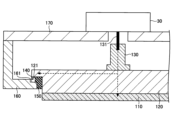
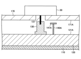
10 プラズマ処理チャンバ(処理容器)
10a 側壁(外壁部材)
30 電源(制御機構)
110 電極プレート
120 保持プレート(第1の導電性部材)
130,130B コンタクタ(第1の導電性部材)
140,140A,140B 通電アクチュエータ(第3の部材)
150 インシュレータ
160 環状部材(第2の導電性部材)
170 上蓋部材(第2の導電性部材)
121,121A,131B 面(第1の面)
161,171A,171B 面(第2の面)
Claims (7)
- 処理容器と、
前記処理容器内に配置される第1の導電性部材と、
前記第1の導電性部材の第1の面と対向する第2の面を有する第2の導電性部材と、
前記第1の導電性部材及び前記第2の導電性部材の少なくとも一方に配置され、温度変化により形状が変化する第3の部材と、
前記第3の部材に前記温度変化を与える制御機構と、を備え、
前記第3の部材の形状が変化することで、前記第1の導電性部材と前記第2の導電性部材との導通又は非導通を切り替える、
プラズマ処理装置。 - 処理容器と、
前記処理容器内に配置される第1の導電性部材と、
前記第1の導電性部材の第1の面と対向する第2の面を有する第2の導電性部材と、
前記第1の導電性部材及び前記第2の導電性部材の少なくとも一方に配置され、温度変化により形状が変化する第3の部材と、
前記第3の部材に電圧又は電流を印加することで前記温度変化を与える電源と、を備え、
前記第1の導電性部材及び前記第2の導電性部材のうち、一方の導電性部材には前記電源から電圧又は電流が印加され、他方の導電性部材は基準電位である、
プラズマ処理装置。 - 前記制御機構は電源であり、前記電源から電圧又は電流を印加することで前記温度変化を与える、
請求項1に記載のプラズマ処理装置。 - 前記第1の導電性部材及び前記第2の導電性部材のうち、一方の導電性部材には前記電源から電圧又は電流が印加され、他方の導電性部材は基準電位である、
請求項3に記載のプラズマ処理装置。
- 前記電圧又は前記電流は、直流である、
請求項2乃至請求項4のいずれか1項に記載のプラズマ処理装置。 - 前記第3の部材は、形状記憶合金部材、圧電部材、バイメタル部材のうち、少なくとも1つを含む、
請求項1乃至請求項5のいずれか1項に記載のプラズマ処理装置。 - 前記第1の導電性部材は上部電極であり、前記第2の導電性部材は前記処理容器の外壁部材と導通する部材である、
請求項1乃至請求項6のいずれか1項に記載のプラズマ処理装置。
Priority Applications (5)
| Application Number | Priority Date | Filing Date | Title |
|---|---|---|---|
| JP2021020071A JP7597464B2 (ja) | 2021-02-10 | 2021-02-10 | プラズマ処理装置 |
| TW111103619A TW202238718A (zh) | 2021-02-10 | 2022-01-27 | 電漿處理裝置 |
| CN202210107398.3A CN114914143A (zh) | 2021-02-10 | 2022-01-28 | 等离子体处理装置 |
| KR1020220016169A KR20220115522A (ko) | 2021-02-10 | 2022-02-08 | 플라스마 처리 장치 |
| US17/666,871 US12148598B2 (en) | 2021-02-10 | 2022-02-08 | Plasma processing apparatus |
Applications Claiming Priority (1)
| Application Number | Priority Date | Filing Date | Title |
|---|---|---|---|
| JP2021020071A JP7597464B2 (ja) | 2021-02-10 | 2021-02-10 | プラズマ処理装置 |
Publications (2)
| Publication Number | Publication Date |
|---|---|
| JP2022122683A JP2022122683A (ja) | 2022-08-23 |
| JP7597464B2 true JP7597464B2 (ja) | 2024-12-10 |
Family
ID=82704698
Family Applications (1)
| Application Number | Title | Priority Date | Filing Date |
|---|---|---|---|
| JP2021020071A Active JP7597464B2 (ja) | 2021-02-10 | 2021-02-10 | プラズマ処理装置 |
Country Status (5)
| Country | Link |
|---|---|
| US (1) | US12148598B2 (ja) |
| JP (1) | JP7597464B2 (ja) |
| KR (1) | KR20220115522A (ja) |
| CN (1) | CN114914143A (ja) |
| TW (1) | TW202238718A (ja) |
Families Citing this family (2)
| Publication number | Priority date | Publication date | Assignee | Title |
|---|---|---|---|---|
| CN111048987B (zh) * | 2019-12-31 | 2021-02-12 | 哈尔滨工业大学 | 基于激光管温度多点采集的高频率复现性激光稳频方法与装置 |
| US20250114806A1 (en) * | 2023-10-06 | 2025-04-10 | Applied Materials, Inc. | Smart faceplate/showerhead using shape memory alloy |
Citations (3)
| Publication number | Priority date | Publication date | Assignee | Title |
|---|---|---|---|---|
| JP2008300414A (ja) | 2007-05-29 | 2008-12-11 | Dainippon Screen Mfg Co Ltd | 薄膜形成装置および薄膜形成方法 |
| US20130199646A1 (en) | 2012-02-07 | 2013-08-08 | Karlsruher Institut Fuer Technologie | Valve plug |
| JP2019536268A (ja) | 2016-11-09 | 2019-12-12 | ラム リサーチ コーポレーションLam Research Corporation | アクティブシャワーヘッド |
Family Cites Families (9)
| Publication number | Priority date | Publication date | Assignee | Title |
|---|---|---|---|---|
| US3699384A (en) * | 1971-09-07 | 1972-10-17 | Hughes Aircraft Co | Offswitching of liquid metal arc switching device by internal current diversion to an auxiliary electrode |
| JPS61241583A (ja) * | 1985-04-19 | 1986-10-27 | Hitachi Micro Comput Eng Ltd | 流量制御装置 |
| JP3039583B2 (ja) * | 1991-05-30 | 2000-05-08 | 株式会社日立製作所 | バルブ及びそれを用いた半導体製造装置 |
| JPH07201828A (ja) * | 1993-12-28 | 1995-08-04 | Tokyo Electron Ltd | シール装置及び処理装置 |
| US6086710A (en) * | 1995-04-07 | 2000-07-11 | Seiko Epson Corporation | Surface treatment apparatus |
| DE19748589C2 (de) * | 1997-11-04 | 1999-12-09 | Marcel Hofsaes | Schalter mit einem temperaturabhängigen Schaltwerk |
| US7951262B2 (en) * | 2004-06-21 | 2011-05-31 | Tokyo Electron Limited | Plasma processing apparatus and method |
| DE102005009057A1 (de) * | 2005-02-28 | 2006-08-31 | Patent-Treuhand-Gesellschaft für elektrische Glühlampen mbH | Starter für Niederdruckentladungslampen |
| JP7345382B2 (ja) | 2018-12-28 | 2023-09-15 | 東京エレクトロン株式会社 | プラズマ処理装置及び制御方法 |
-
2021
- 2021-02-10 JP JP2021020071A patent/JP7597464B2/ja active Active
-
2022
- 2022-01-27 TW TW111103619A patent/TW202238718A/zh unknown
- 2022-01-28 CN CN202210107398.3A patent/CN114914143A/zh active Pending
- 2022-02-08 US US17/666,871 patent/US12148598B2/en active Active
- 2022-02-08 KR KR1020220016169A patent/KR20220115522A/ko active Pending
Patent Citations (3)
| Publication number | Priority date | Publication date | Assignee | Title |
|---|---|---|---|---|
| JP2008300414A (ja) | 2007-05-29 | 2008-12-11 | Dainippon Screen Mfg Co Ltd | 薄膜形成装置および薄膜形成方法 |
| US20130199646A1 (en) | 2012-02-07 | 2013-08-08 | Karlsruher Institut Fuer Technologie | Valve plug |
| JP2019536268A (ja) | 2016-11-09 | 2019-12-12 | ラム リサーチ コーポレーションLam Research Corporation | アクティブシャワーヘッド |
Also Published As
| Publication number | Publication date |
|---|---|
| US12148598B2 (en) | 2024-11-19 |
| US20220254611A1 (en) | 2022-08-11 |
| JP2022122683A (ja) | 2022-08-23 |
| CN114914143A (zh) | 2022-08-16 |
| TW202238718A (zh) | 2022-10-01 |
| KR20220115522A (ko) | 2022-08-17 |
Similar Documents
| Publication | Publication Date | Title |
|---|---|---|
| JP7632980B2 (ja) | 載置台及びプラズマ処理装置 | |
| JP2023033282A (ja) | 基板支持体及び基板処理装置 | |
| JP7597464B2 (ja) | プラズマ処理装置 | |
| KR20210116261A (ko) | 플라즈마 처리 장치 | |
| JP2025157531A (ja) | プラズマ処理装置 | |
| JP7419611B1 (ja) | 伝熱ガスのリーク量低減方法 | |
| JP2021166251A (ja) | 基板処理装置 | |
| WO2023074475A1 (ja) | プラズマ処理装置及び静電チャック | |
| WO2022215633A1 (ja) | 静電チャックおよび基板処理装置 | |
| JP2023004431A (ja) | プラズマ処理装置 | |
| WO2024057973A1 (ja) | 静電チャック及び基板処理装置 | |
| KR20240121307A (ko) | 기판 지지기 및 플라즈마 처리 장치 | |
| JP2023165222A (ja) | 静電チャック、基板支持アセンブリ、及びプラズマ処理装置 | |
| JP7723172B1 (ja) | 静電チャック | |
| US20250357174A1 (en) | Substrate support and method of regenerating substrate support | |
| JP7572126B2 (ja) | プラズマ処理装置用の電極及びプラズマ処理装置 | |
| WO2025263340A1 (ja) | 基板支持器及び基板処理装置 | |
| WO2025047428A1 (ja) | プラズマエッチング装置、電源ユニット及びプラズマエッチング方法 | |
| WO2025169740A1 (ja) | プラズマ処理装置、電源システム、制御方法、及びプログラム | |
| WO2024257401A1 (ja) | プラズマ処理装置 | |
| WO2024135385A1 (ja) | プラズマ処理装置及び制御方法 | |
| JP2025127899A (ja) | プラズマ処理装置 | |
| WO2025126937A1 (ja) | 被膜形成方法、プラズマ処理方法、及び、プラズマ処理装置 | |
| JP2023056629A (ja) | プラズマ処理装置 | |
| WO2024150693A1 (ja) | 支持体、基板支持器及びプラズマ処理装置 |
Legal Events
| Date | Code | Title | Description |
|---|---|---|---|
| A621 | Written request for application examination |
Free format text: JAPANESE INTERMEDIATE CODE: A621 Effective date: 20231108 |
|
| A977 | Report on retrieval |
Free format text: JAPANESE INTERMEDIATE CODE: A971007 Effective date: 20240718 |
|
| A131 | Notification of reasons for refusal |
Free format text: JAPANESE INTERMEDIATE CODE: A131 Effective date: 20240723 |
|
| A521 | Request for written amendment filed |
Free format text: JAPANESE INTERMEDIATE CODE: A523 Effective date: 20240920 |
|
| TRDD | Decision of grant or rejection written | ||
| A01 | Written decision to grant a patent or to grant a registration (utility model) |
Free format text: JAPANESE INTERMEDIATE CODE: A01 Effective date: 20241029 |
|
| A61 | First payment of annual fees (during grant procedure) |
Free format text: JAPANESE INTERMEDIATE CODE: A61 Effective date: 20241126 |
|
| R150 | Certificate of patent or registration of utility model |
Ref document number: 7597464 Country of ref document: JP Free format text: JAPANESE INTERMEDIATE CODE: R150 |