JP7597339B2 - 積層体及び積層体の製造方法 - Google Patents
積層体及び積層体の製造方法 Download PDFInfo
- Publication number
- JP7597339B2 JP7597339B2 JP2023527634A JP2023527634A JP7597339B2 JP 7597339 B2 JP7597339 B2 JP 7597339B2 JP 2023527634 A JP2023527634 A JP 2023527634A JP 2023527634 A JP2023527634 A JP 2023527634A JP 7597339 B2 JP7597339 B2 JP 7597339B2
- Authority
- JP
- Japan
- Prior art keywords
- glass substrate
- amorphous glass
- aln layer
- less
- film formation
- Prior art date
- Legal status (The legal status is an assumption and is not a legal conclusion. Google has not performed a legal analysis and makes no representation as to the accuracy of the status listed.)
- Active
Links
Images

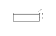


Classifications
-
- C—CHEMISTRY; METALLURGY
- C30—CRYSTAL GROWTH
- C30B—SINGLE-CRYSTAL GROWTH; UNIDIRECTIONAL SOLIDIFICATION OF EUTECTIC MATERIAL OR UNIDIRECTIONAL DEMIXING OF EUTECTOID MATERIAL; REFINING BY ZONE-MELTING OF MATERIAL; PRODUCTION OF A HOMOGENEOUS POLYCRYSTALLINE MATERIAL WITH DEFINED STRUCTURE; SINGLE CRYSTALS OR HOMOGENEOUS POLYCRYSTALLINE MATERIAL WITH DEFINED STRUCTURE; AFTER-TREATMENT OF SINGLE CRYSTALS OR A HOMOGENEOUS POLYCRYSTALLINE MATERIAL WITH DEFINED STRUCTURE; APPARATUS THEREFOR
- C30B29/00—Single crystals or homogeneous polycrystalline material with defined structure characterised by the material or by their shape
- C30B29/10—Inorganic compounds or compositions
- C30B29/38—Nitrides
-
- C—CHEMISTRY; METALLURGY
- C30—CRYSTAL GROWTH
- C30B—SINGLE-CRYSTAL GROWTH; UNIDIRECTIONAL SOLIDIFICATION OF EUTECTIC MATERIAL OR UNIDIRECTIONAL DEMIXING OF EUTECTOID MATERIAL; REFINING BY ZONE-MELTING OF MATERIAL; PRODUCTION OF A HOMOGENEOUS POLYCRYSTALLINE MATERIAL WITH DEFINED STRUCTURE; SINGLE CRYSTALS OR HOMOGENEOUS POLYCRYSTALLINE MATERIAL WITH DEFINED STRUCTURE; AFTER-TREATMENT OF SINGLE CRYSTALS OR A HOMOGENEOUS POLYCRYSTALLINE MATERIAL WITH DEFINED STRUCTURE; APPARATUS THEREFOR
- C30B29/00—Single crystals or homogeneous polycrystalline material with defined structure characterised by the material or by their shape
- C30B29/10—Inorganic compounds or compositions
- C30B29/40—AIIIBV compounds wherein A is B, Al, Ga, In or Tl and B is N, P, As, Sb or Bi
-
- H—ELECTRICITY
- H10—SEMICONDUCTOR DEVICES; ELECTRIC SOLID-STATE DEVICES NOT OTHERWISE PROVIDED FOR
- H10D—INORGANIC ELECTRIC SEMICONDUCTOR DEVICES
- H10D30/00—Field-effect transistors [FET]
- H10D30/01—Manufacture or treatment
- H10D30/015—Manufacture or treatment of FETs having heterojunction interface channels or heterojunction gate electrodes, e.g. HEMT
-
- H—ELECTRICITY
- H10—SEMICONDUCTOR DEVICES; ELECTRIC SOLID-STATE DEVICES NOT OTHERWISE PROVIDED FOR
- H10H—INORGANIC LIGHT-EMITTING SEMICONDUCTOR DEVICES HAVING POTENTIAL BARRIERS
- H10H20/00—Individual inorganic light-emitting semiconductor devices having potential barriers, e.g. light-emitting diodes [LED]
- H10H20/01—Manufacture or treatment
- H10H20/011—Manufacture or treatment of bodies, e.g. forming semiconductor layers
- H10H20/013—Manufacture or treatment of bodies, e.g. forming semiconductor layers having light-emitting regions comprising only Group III-V materials
- H10H20/0133—Manufacture or treatment of bodies, e.g. forming semiconductor layers having light-emitting regions comprising only Group III-V materials with a substrate not being Group III-V materials
- H10H20/01335—Manufacture or treatment of bodies, e.g. forming semiconductor layers having light-emitting regions comprising only Group III-V materials with a substrate not being Group III-V materials the light-emitting regions comprising nitride materials
-
- H—ELECTRICITY
- H10—SEMICONDUCTOR DEVICES; ELECTRIC SOLID-STATE DEVICES NOT OTHERWISE PROVIDED FOR
- H10H—INORGANIC LIGHT-EMITTING SEMICONDUCTOR DEVICES HAVING POTENTIAL BARRIERS
- H10H20/00—Individual inorganic light-emitting semiconductor devices having potential barriers, e.g. light-emitting diodes [LED]
- H10H20/80—Constructional details
- H10H20/81—Bodies
- H10H20/817—Bodies characterised by the crystal structures or orientations, e.g. polycrystalline, amorphous or porous
-
- H—ELECTRICITY
- H10—SEMICONDUCTOR DEVICES; ELECTRIC SOLID-STATE DEVICES NOT OTHERWISE PROVIDED FOR
- H10P—GENERIC PROCESSES OR APPARATUS FOR THE MANUFACTURE OR TREATMENT OF DEVICES COVERED BY CLASS H10
- H10P14/00—Formation of materials, e.g. in the shape of layers or pillars
- H10P14/20—Formation of materials, e.g. in the shape of layers or pillars of semiconductor materials
- H10P14/22—Formation of materials, e.g. in the shape of layers or pillars of semiconductor materials using physical deposition, e.g. vacuum deposition or sputtering
-
- H—ELECTRICITY
- H10—SEMICONDUCTOR DEVICES; ELECTRIC SOLID-STATE DEVICES NOT OTHERWISE PROVIDED FOR
- H10P—GENERIC PROCESSES OR APPARATUS FOR THE MANUFACTURE OR TREATMENT OF DEVICES COVERED BY CLASS H10
- H10P14/00—Formation of materials, e.g. in the shape of layers or pillars
- H10P14/20—Formation of materials, e.g. in the shape of layers or pillars of semiconductor materials
- H10P14/29—Formation of materials, e.g. in the shape of layers or pillars of semiconductor materials characterised by the substrates
- H10P14/2901—Materials
- H10P14/2922—Materials being non-crystalline insulating materials, e.g. glass or polymers
-
- H—ELECTRICITY
- H10—SEMICONDUCTOR DEVICES; ELECTRIC SOLID-STATE DEVICES NOT OTHERWISE PROVIDED FOR
- H10P—GENERIC PROCESSES OR APPARATUS FOR THE MANUFACTURE OR TREATMENT OF DEVICES COVERED BY CLASS H10
- H10P14/00—Formation of materials, e.g. in the shape of layers or pillars
- H10P14/20—Formation of materials, e.g. in the shape of layers or pillars of semiconductor materials
- H10P14/29—Formation of materials, e.g. in the shape of layers or pillars of semiconductor materials characterised by the substrates
- H10P14/2924—Structures
- H10P14/2925—Surface structures
-
- H—ELECTRICITY
- H10—SEMICONDUCTOR DEVICES; ELECTRIC SOLID-STATE DEVICES NOT OTHERWISE PROVIDED FOR
- H10P—GENERIC PROCESSES OR APPARATUS FOR THE MANUFACTURE OR TREATMENT OF DEVICES COVERED BY CLASS H10
- H10P14/00—Formation of materials, e.g. in the shape of layers or pillars
- H10P14/20—Formation of materials, e.g. in the shape of layers or pillars of semiconductor materials
- H10P14/34—Deposited materials, e.g. layers
- H10P14/3402—Deposited materials, e.g. layers characterised by the chemical composition
- H10P14/3414—Deposited materials, e.g. layers characterised by the chemical composition being group IIIA-VIA materials
- H10P14/3416—Nitrides
-
- H—ELECTRICITY
- H10—SEMICONDUCTOR DEVICES; ELECTRIC SOLID-STATE DEVICES NOT OTHERWISE PROVIDED FOR
- H10P—GENERIC PROCESSES OR APPARATUS FOR THE MANUFACTURE OR TREATMENT OF DEVICES COVERED BY CLASS H10
- H10P14/00—Formation of materials, e.g. in the shape of layers or pillars
- H10P14/20—Formation of materials, e.g. in the shape of layers or pillars of semiconductor materials
- H10P14/34—Deposited materials, e.g. layers
- H10P14/3466—Crystal orientation
-
- H—ELECTRICITY
- H10—SEMICONDUCTOR DEVICES; ELECTRIC SOLID-STATE DEVICES NOT OTHERWISE PROVIDED FOR
- H10D—INORGANIC ELECTRIC SEMICONDUCTOR DEVICES
- H10D30/00—Field-effect transistors [FET]
- H10D30/40—FETs having zero-dimensional [0D], one-dimensional [1D] or two-dimensional [2D] charge carrier gas channels
- H10D30/47—FETs having zero-dimensional [0D], one-dimensional [1D] or two-dimensional [2D] charge carrier gas channels having two-dimensional [2D] charge carrier gas channels, e.g. nanoribbon FETs or high electron mobility transistors [HEMT]
- H10D30/471—High electron mobility transistors [HEMT] or high hole mobility transistors [HHMT]
- H10D30/475—High electron mobility transistors [HEMT] or high hole mobility transistors [HHMT] having wider bandgap layer formed on top of lower bandgap active layer, e.g. undoped barrier HEMTs such as i-AlGaN/GaN HEMTs
-
- H—ELECTRICITY
- H10—SEMICONDUCTOR DEVICES; ELECTRIC SOLID-STATE DEVICES NOT OTHERWISE PROVIDED FOR
- H10D—INORGANIC ELECTRIC SEMICONDUCTOR DEVICES
- H10D62/00—Semiconductor bodies, or regions thereof, of devices having potential barriers
- H10D62/10—Shapes, relative sizes or dispositions of the regions of the semiconductor bodies; Shapes of the semiconductor bodies
- H10D62/17—Semiconductor regions connected to electrodes not carrying current to be rectified, amplified or switched, e.g. channel regions
- H10D62/343—Gate regions of field-effect devices having PN junction gates
-
- H—ELECTRICITY
- H10—SEMICONDUCTOR DEVICES; ELECTRIC SOLID-STATE DEVICES NOT OTHERWISE PROVIDED FOR
- H10D—INORGANIC ELECTRIC SEMICONDUCTOR DEVICES
- H10D62/00—Semiconductor bodies, or regions thereof, of devices having potential barriers
- H10D62/80—Semiconductor bodies, or regions thereof, of devices having potential barriers characterised by the materials
- H10D62/85—Semiconductor bodies, or regions thereof, of devices having potential barriers characterised by the materials being Group III-V materials, e.g. GaAs
- H10D62/8503—Nitride Group III-V materials, e.g. AlN or GaN
-
- H—ELECTRICITY
- H10—SEMICONDUCTOR DEVICES; ELECTRIC SOLID-STATE DEVICES NOT OTHERWISE PROVIDED FOR
- H10H—INORGANIC LIGHT-EMITTING SEMICONDUCTOR DEVICES HAVING POTENTIAL BARRIERS
- H10H20/00—Individual inorganic light-emitting semiconductor devices having potential barriers, e.g. light-emitting diodes [LED]
- H10H20/80—Constructional details
- H10H20/81—Bodies
- H10H20/822—Materials of the light-emitting regions
- H10H20/824—Materials of the light-emitting regions comprising only Group III-V materials, e.g. GaP
- H10H20/825—Materials of the light-emitting regions comprising only Group III-V materials, e.g. GaP containing nitrogen, e.g. GaN
-
- H—ELECTRICITY
- H10—SEMICONDUCTOR DEVICES; ELECTRIC SOLID-STATE DEVICES NOT OTHERWISE PROVIDED FOR
- H10P—GENERIC PROCESSES OR APPARATUS FOR THE MANUFACTURE OR TREATMENT OF DEVICES COVERED BY CLASS H10
- H10P14/00—Formation of materials, e.g. in the shape of layers or pillars
- H10P14/20—Formation of materials, e.g. in the shape of layers or pillars of semiconductor materials
- H10P14/29—Formation of materials, e.g. in the shape of layers or pillars of semiconductor materials characterised by the substrates
- H10P14/2901—Materials
- H10P14/2921—Materials being crystalline insulating materials
Landscapes
- Chemical & Material Sciences (AREA)
- Inorganic Chemistry (AREA)
- Engineering & Computer Science (AREA)
- Crystallography & Structural Chemistry (AREA)
- Materials Engineering (AREA)
- Metallurgy (AREA)
- Organic Chemistry (AREA)
- Physical Vapour Deposition (AREA)
- Ceramic Capacitors (AREA)
- Crystals, And After-Treatments Of Crystals (AREA)
Applications Claiming Priority (3)
| Application Number | Priority Date | Filing Date | Title |
|---|---|---|---|
| JP2021098291 | 2021-06-11 | ||
| JP2021098291 | 2021-06-11 | ||
| PCT/JP2022/022163 WO2022259918A1 (ja) | 2021-06-11 | 2022-05-31 | 積層体及び積層体の製造方法 |
Publications (3)
| Publication Number | Publication Date |
|---|---|
| JPWO2022259918A1 JPWO2022259918A1 (https=) | 2022-12-15 |
| JPWO2022259918A5 JPWO2022259918A5 (https=) | 2024-04-22 |
| JP7597339B2 true JP7597339B2 (ja) | 2024-12-10 |
Family
ID=84424910
Family Applications (1)
| Application Number | Title | Priority Date | Filing Date |
|---|---|---|---|
| JP2023527634A Active JP7597339B2 (ja) | 2021-06-11 | 2022-05-31 | 積層体及び積層体の製造方法 |
Country Status (5)
| Country | Link |
|---|---|
| US (1) | US20240113174A1 (https=) |
| JP (1) | JP7597339B2 (https=) |
| CN (1) | CN117441225A (https=) |
| TW (1) | TWI816428B (https=) |
| WO (1) | WO2022259918A1 (https=) |
Families Citing this family (1)
| Publication number | Priority date | Publication date | Assignee | Title |
|---|---|---|---|---|
| WO2024181028A1 (ja) * | 2023-02-28 | 2024-09-06 | 株式会社ジャパンディスプレイ | Led素子、ledアレイ基板及びled素子の製造方法 |
Citations (3)
| Publication number | Priority date | Publication date | Assignee | Title |
|---|---|---|---|---|
| US20080289420A1 (en) | 2004-07-01 | 2008-11-27 | The University Of Paisley | Ultrasound Transducers |
| JP2012224539A (ja) | 2011-04-19 | 2012-11-15 | Samsung Electronics Co Ltd | GaN薄膜構造物、その製造方法、及びそれを含む半導体素子 |
| CN103334090A (zh) | 2013-07-17 | 2013-10-02 | 辽宁太阳能研究应用有限公司 | InN/AlN/玻璃结构的制备方法 |
Family Cites Families (5)
| Publication number | Priority date | Publication date | Assignee | Title |
|---|---|---|---|---|
| JPH07109573A (ja) * | 1993-10-12 | 1995-04-25 | Semiconductor Energy Lab Co Ltd | ガラス基板および加熱処理方法 |
| WO2013158210A2 (en) * | 2012-02-17 | 2013-10-24 | Yale University | Heterogeneous material integration through guided lateral growth |
| DE102014104798B4 (de) * | 2014-04-03 | 2021-04-22 | Schott Ag | Harte anti-Reflex-Beschichtungen sowie deren Herstellung und Verwendung |
| WO2015181648A1 (en) * | 2014-05-27 | 2015-12-03 | The Silanna Group Pty Limited | An optoelectronic device |
| TWI892641B (zh) * | 2019-01-31 | 2025-08-01 | 美商伊雷克托科學工業股份有限公司 | 光學系統 |
-
2022
- 2022-05-31 CN CN202280040757.6A patent/CN117441225A/zh active Pending
- 2022-05-31 WO PCT/JP2022/022163 patent/WO2022259918A1/ja not_active Ceased
- 2022-05-31 JP JP2023527634A patent/JP7597339B2/ja active Active
- 2022-06-09 TW TW111121384A patent/TWI816428B/zh active
-
2023
- 2023-12-07 US US18/532,505 patent/US20240113174A1/en active Pending
Patent Citations (3)
| Publication number | Priority date | Publication date | Assignee | Title |
|---|---|---|---|---|
| US20080289420A1 (en) | 2004-07-01 | 2008-11-27 | The University Of Paisley | Ultrasound Transducers |
| JP2012224539A (ja) | 2011-04-19 | 2012-11-15 | Samsung Electronics Co Ltd | GaN薄膜構造物、その製造方法、及びそれを含む半導体素子 |
| CN103334090A (zh) | 2013-07-17 | 2013-10-02 | 辽宁太阳能研究应用有限公司 | InN/AlN/玻璃结构的制备方法 |
Non-Patent Citations (1)
| Title |
|---|
| KUSAKA, K. et al.,Effect of sputtering gas pressure and nitrogen concentration on crystal orientation and residual stress in sputtered AlN films,Vacuum,2002年,Vol. 66,pp. 441-446 |
Also Published As
| Publication number | Publication date |
|---|---|
| CN117441225A (zh) | 2024-01-23 |
| TWI816428B (zh) | 2023-09-21 |
| WO2022259918A1 (ja) | 2022-12-15 |
| US20240113174A1 (en) | 2024-04-04 |
| JPWO2022259918A1 (https=) | 2022-12-15 |
| TW202304708A (zh) | 2023-02-01 |
Similar Documents
| Publication | Publication Date | Title |
|---|---|---|
| TWI394289B (zh) | 以單晶氮化物為主之半導體基底及使用彼以製造高品質以氮化物為主之發光裝置的方法 | |
| KR101525907B1 (ko) | 질화물 반도체 구조 및 그 제작방법 | |
| KR101650840B1 (ko) | 발광소자 및 이의 제조방법 | |
| US8791468B2 (en) | GaN film structure, method of fabricating the same, and semiconductor device including the same | |
| US8882910B2 (en) | AlGaN substrate and production method thereof | |
| CN102024887B (zh) | 含有铝的氮化物中间层的制造方法、氮化物层的制造方法和氮化物半导体元件的制造方法 | |
| JP5631034B2 (ja) | 窒化物半導体エピタキシャル基板 | |
| WO2006126330A1 (ja) | GaN単結晶成長方法,GaN基板作製方法,GaN系素子製造方法およびGaN系素子 | |
| JP2008034834A (ja) | シリコン基板上の窒化物単結晶成長方法、これを用いた窒化物半導体発光素子及びその製造方法 | |
| KR20050097076A (ko) | 외부양자효율이 개선된 질화물 반도체 및 그 제조방법 | |
| JP2010232322A (ja) | 化合物半導体基板 | |
| JP4860736B2 (ja) | 半導体構造物及びそれを製造する方法 | |
| JP4996448B2 (ja) | 半導体基板の作成方法 | |
| CN103050594B (zh) | 氮化物半导体结构的制造方法 | |
| JP7597339B2 (ja) | 積層体及び積層体の製造方法 | |
| JP7785929B2 (ja) | 半導体デバイス及びその作製方法 | |
| JP6242238B2 (ja) | 窒化物半導体多元混晶の製造方法 | |
| CN103137801A (zh) | 在钻石基板上形成的磊晶层结构及其制造方法 | |
| KR20070100852A (ko) | 호모에피택셜 기판 및 발광 다층구조체 성장용 템플렛을 이용한 그룹 3족 질화물계 반도체 수직구조의 발광소자 제작 | |
| KR20070100851A (ko) | 양질의 그룹 3족 질화물계 단결정 반도체 박막층 성장을위한 호모에피택셜 기판 및 발광 다층구조체 성장용 템플렛제작 및 성장 | |
| JPH10303510A (ja) | Iii 族窒化物半導体素子およびその製造方法 | |
| JP5746544B2 (ja) | 窒化物半導体用基板および窒化物半導体用基板の製造方法 | |
| CN105789396A (zh) | 一种不易发生翘曲的大尺寸发光二极管外延片制作方法 | |
| CN108110108B (zh) | Si基LED外延片及制造方法 | |
| WO2025239101A1 (ja) | 積層構造体、発光素子、および半導体装置 |
Legal Events
| Date | Code | Title | Description |
|---|---|---|---|
| A521 | Request for written amendment filed |
Free format text: JAPANESE INTERMEDIATE CODE: A523 Effective date: 20231206 |
|
| A621 | Written request for application examination |
Free format text: JAPANESE INTERMEDIATE CODE: A621 Effective date: 20231206 |
|
| AA64 | Notification of invalidation of claim of internal priority (with term) |
Free format text: JAPANESE INTERMEDIATE CODE: A241764 Effective date: 20240305 |
|
| A521 | Request for written amendment filed |
Free format text: JAPANESE INTERMEDIATE CODE: A523 Effective date: 20240319 |
|
| TRDD | Decision of grant or rejection written | ||
| A01 | Written decision to grant a patent or to grant a registration (utility model) |
Free format text: JAPANESE INTERMEDIATE CODE: A01 Effective date: 20241022 |
|
| A61 | First payment of annual fees (during grant procedure) |
Free format text: JAPANESE INTERMEDIATE CODE: A61 Effective date: 20241120 |
|
| R150 | Certificate of patent or registration of utility model |
Ref document number: 7597339 Country of ref document: JP Free format text: JAPANESE INTERMEDIATE CODE: R150 |