JP7586082B2 - 炭化珪素半導体装置 - Google Patents
炭化珪素半導体装置 Download PDFInfo
- Publication number
- JP7586082B2 JP7586082B2 JP2021537274A JP2021537274A JP7586082B2 JP 7586082 B2 JP7586082 B2 JP 7586082B2 JP 2021537274 A JP2021537274 A JP 2021537274A JP 2021537274 A JP2021537274 A JP 2021537274A JP 7586082 B2 JP7586082 B2 JP 7586082B2
- Authority
- JP
- Japan
- Prior art keywords
- sidewall
- semiconductor layer
- region
- insulating film
- silicon carbide
- Prior art date
- Legal status (The legal status is an assumption and is not a legal conclusion. Google has not performed a legal analysis and makes no representation as to the accuracy of the status listed.)
- Active
Links
Images


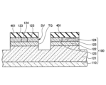


Classifications
-
- H—ELECTRICITY
- H10—SEMICONDUCTOR DEVICES; ELECTRIC SOLID-STATE DEVICES NOT OTHERWISE PROVIDED FOR
- H10D—INORGANIC ELECTRIC SEMICONDUCTOR DEVICES
- H10D30/00—Field-effect transistors [FET]
- H10D30/60—Insulated-gate field-effect transistors [IGFET]
- H10D30/64—Double-diffused metal-oxide semiconductor [DMOS] FETs
- H10D30/66—Vertical DMOS [VDMOS] FETs
- H10D30/668—Vertical DMOS [VDMOS] FETs having trench gate electrodes, e.g. UMOS transistors
-
- H—ELECTRICITY
- H10—SEMICONDUCTOR DEVICES; ELECTRIC SOLID-STATE DEVICES NOT OTHERWISE PROVIDED FOR
- H10D—INORGANIC ELECTRIC SEMICONDUCTOR DEVICES
- H10D12/00—Bipolar devices controlled by the field effect, e.g. insulated-gate bipolar transistors [IGBT]
-
- H—ELECTRICITY
- H10—SEMICONDUCTOR DEVICES; ELECTRIC SOLID-STATE DEVICES NOT OTHERWISE PROVIDED FOR
- H10D—INORGANIC ELECTRIC SEMICONDUCTOR DEVICES
- H10D30/00—Field-effect transistors [FET]
- H10D30/01—Manufacture or treatment
- H10D30/021—Manufacture or treatment of FETs having insulated gates [IGFET]
- H10D30/028—Manufacture or treatment of FETs having insulated gates [IGFET] of double-diffused metal oxide semiconductor [DMOS] FETs
- H10D30/0291—Manufacture or treatment of FETs having insulated gates [IGFET] of double-diffused metal oxide semiconductor [DMOS] FETs of vertical DMOS [VDMOS] FETs
- H10D30/0297—Manufacture or treatment of FETs having insulated gates [IGFET] of double-diffused metal oxide semiconductor [DMOS] FETs of vertical DMOS [VDMOS] FETs using recessing of the gate electrodes, e.g. to form trench gate electrodes
-
- H—ELECTRICITY
- H10—SEMICONDUCTOR DEVICES; ELECTRIC SOLID-STATE DEVICES NOT OTHERWISE PROVIDED FOR
- H10D—INORGANIC ELECTRIC SEMICONDUCTOR DEVICES
- H10D62/00—Semiconductor bodies, or regions thereof, of devices having potential barriers
- H10D62/80—Semiconductor bodies, or regions thereof, of devices having potential barriers characterised by the materials
- H10D62/83—Semiconductor bodies, or regions thereof, of devices having potential barriers characterised by the materials being Group IV materials, e.g. B-doped Si or undoped Ge
- H10D62/832—Semiconductor bodies, or regions thereof, of devices having potential barriers characterised by the materials being Group IV materials, e.g. B-doped Si or undoped Ge being Group IV materials comprising two or more elements, e.g. SiGe
- H10D62/8325—Silicon carbide
-
- H—ELECTRICITY
- H10—SEMICONDUCTOR DEVICES; ELECTRIC SOLID-STATE DEVICES NOT OTHERWISE PROVIDED FOR
- H10D—INORGANIC ELECTRIC SEMICONDUCTOR DEVICES
- H10D64/00—Electrodes of devices having potential barriers
- H10D64/20—Electrodes characterised by their shapes, relative sizes or dispositions
- H10D64/27—Electrodes not carrying the current to be rectified, amplified, oscillated or switched, e.g. gates
- H10D64/311—Gate electrodes for field-effect devices
- H10D64/411—Gate electrodes for field-effect devices for FETs
- H10D64/511—Gate electrodes for field-effect devices for FETs for IGFETs
- H10D64/514—Gate electrodes for field-effect devices for FETs for IGFETs characterised by the insulating layers
- H10D64/516—Gate electrodes for field-effect devices for FETs for IGFETs characterised by the insulating layers the thicknesses being non-uniform
Landscapes
- Electrodes Of Semiconductors (AREA)
Applications Claiming Priority (3)
| Application Number | Priority Date | Filing Date | Title |
|---|---|---|---|
| JP2019144751 | 2019-08-06 | ||
| JP2019144751 | 2019-08-06 | ||
| PCT/JP2020/029300 WO2021024916A1 (ja) | 2019-08-06 | 2020-07-30 | 炭化珪素半導体装置 |
Publications (2)
| Publication Number | Publication Date |
|---|---|
| JPWO2021024916A1 JPWO2021024916A1 (https=) | 2021-02-11 |
| JP7586082B2 true JP7586082B2 (ja) | 2024-11-19 |
Family
ID=74504109
Family Applications (1)
| Application Number | Title | Priority Date | Filing Date |
|---|---|---|---|
| JP2021537274A Active JP7586082B2 (ja) | 2019-08-06 | 2020-07-30 | 炭化珪素半導体装置 |
Country Status (2)
| Country | Link |
|---|---|
| JP (1) | JP7586082B2 (https=) |
| WO (1) | WO2021024916A1 (https=) |
Citations (6)
| Publication number | Priority date | Publication date | Assignee | Title |
|---|---|---|---|---|
| WO2012127821A1 (ja) | 2011-03-23 | 2012-09-27 | パナソニック株式会社 | 半導体装置およびその製造方法 |
| WO2014148130A1 (ja) | 2013-03-19 | 2014-09-25 | 住友電気工業株式会社 | 炭化珪素半導体装置およびその製造方法 |
| JP2016164906A (ja) | 2015-03-06 | 2016-09-08 | 豊田合成株式会社 | 半導体装置およびその製造方法ならびに電力変換装置 |
| US20160351668A1 (en) | 2015-05-28 | 2016-12-01 | Infineon Technologies Ag | Stripe-Shaped Electrode Structure Including a Main Portion with a Field Electrode and an End Portion Terminating the Electrode Structure |
| JP2016213421A (ja) | 2015-05-13 | 2016-12-15 | 株式会社豊田中央研究所 | 半導体装置 |
| JP2018093135A (ja) | 2016-12-07 | 2018-06-14 | 株式会社東芝 | 半導体装置及びその製造方法 |
-
2020
- 2020-07-30 JP JP2021537274A patent/JP7586082B2/ja active Active
- 2020-07-30 WO PCT/JP2020/029300 patent/WO2021024916A1/ja not_active Ceased
Patent Citations (6)
| Publication number | Priority date | Publication date | Assignee | Title |
|---|---|---|---|---|
| WO2012127821A1 (ja) | 2011-03-23 | 2012-09-27 | パナソニック株式会社 | 半導体装置およびその製造方法 |
| WO2014148130A1 (ja) | 2013-03-19 | 2014-09-25 | 住友電気工業株式会社 | 炭化珪素半導体装置およびその製造方法 |
| JP2016164906A (ja) | 2015-03-06 | 2016-09-08 | 豊田合成株式会社 | 半導体装置およびその製造方法ならびに電力変換装置 |
| JP2016213421A (ja) | 2015-05-13 | 2016-12-15 | 株式会社豊田中央研究所 | 半導体装置 |
| US20160351668A1 (en) | 2015-05-28 | 2016-12-01 | Infineon Technologies Ag | Stripe-Shaped Electrode Structure Including a Main Portion with a Field Electrode and an End Portion Terminating the Electrode Structure |
| JP2018093135A (ja) | 2016-12-07 | 2018-06-14 | 株式会社東芝 | 半導体装置及びその製造方法 |
Also Published As
| Publication number | Publication date |
|---|---|
| JPWO2021024916A1 (https=) | 2021-02-11 |
| WO2021024916A1 (ja) | 2021-02-11 |
Similar Documents
| Publication | Publication Date | Title |
|---|---|---|
| CN102971853B (zh) | 半导体器件及其制造方法 | |
| US9276106B2 (en) | Silicon carbide semiconductor device and method for manufacturing same | |
| US8999854B2 (en) | Method for manufacturing silicon carbide semiconductor device | |
| JP6135364B2 (ja) | 炭化珪素半導体装置およびその製造方法 | |
| CN103782391B (zh) | 碳化硅半导体器件及其制造方法 | |
| JP7156314B2 (ja) | 炭化珪素半導体装置 | |
| US9984879B2 (en) | Silicon carbide semiconductor device and method for manufacturing same | |
| CN103890952B (zh) | 碳化硅半导体器件及其制造方法 | |
| US9627487B2 (en) | Method for manufacturing silicon carbide semiconductor device and silicon carbide semiconductor device | |
| JP6075120B2 (ja) | 炭化珪素半導体装置 | |
| US9543412B2 (en) | Method for manufacturing silicon carbide semiconductor device | |
| JP7586082B2 (ja) | 炭化珪素半導体装置 | |
| JP2024125439A (ja) | 半導体装置及び半導体装置の製造方法 | |
| JP7156313B2 (ja) | 炭化珪素半導体装置 | |
| JP7722202B2 (ja) | 炭化珪素半導体装置 | |
| US9679986B2 (en) | Silicon carbide semiconductor device | |
| US9793365B2 (en) | Method for manufacturing silicon carbide semiconductor device having trench | |
| WO2023026803A1 (ja) | 炭化珪素半導体装置及び炭化珪素半導体装置の製造方法 | |
| WO2022137649A1 (ja) | 炭化珪素半導体装置 | |
| WO2022209089A1 (ja) | 炭化珪素半導体装置 |
Legal Events
| Date | Code | Title | Description |
|---|---|---|---|
| A621 | Written request for application examination |
Free format text: JAPANESE INTERMEDIATE CODE: A621 Effective date: 20230421 |
|
| A131 | Notification of reasons for refusal |
Free format text: JAPANESE INTERMEDIATE CODE: A131 Effective date: 20240618 |
|
| A521 | Request for written amendment filed |
Free format text: JAPANESE INTERMEDIATE CODE: A523 Effective date: 20240806 |
|
| TRDD | Decision of grant or rejection written | ||
| A01 | Written decision to grant a patent or to grant a registration (utility model) |
Free format text: JAPANESE INTERMEDIATE CODE: A01 Effective date: 20241008 |
|
| A61 | First payment of annual fees (during grant procedure) |
Free format text: JAPANESE INTERMEDIATE CODE: A61 Effective date: 20241021 |
|
| R150 | Certificate of patent or registration of utility model |
Ref document number: 7586082 Country of ref document: JP Free format text: JAPANESE INTERMEDIATE CODE: R150 |
|
| S111 | Request for change of ownership or part of ownership |
Free format text: JAPANESE INTERMEDIATE CODE: R313113 |