JP7582425B2 - Manufacturing method of film adhesive for semiconductor - Google Patents
Manufacturing method of film adhesive for semiconductor Download PDFInfo
- Publication number
- JP7582425B2 JP7582425B2 JP2023181615A JP2023181615A JP7582425B2 JP 7582425 B2 JP7582425 B2 JP 7582425B2 JP 2023181615 A JP2023181615 A JP 2023181615A JP 2023181615 A JP2023181615 A JP 2023181615A JP 7582425 B2 JP7582425 B2 JP 7582425B2
- Authority
- JP
- Japan
- Prior art keywords
- adhesive
- film
- resin
- layer
- component
- Prior art date
- Legal status (The legal status is an assumption and is not a legal conclusion. Google has not performed a legal analysis and makes no representation as to the accuracy of the status listed.)
- Active
Links
Images


Classifications
-
- B—PERFORMING OPERATIONS; TRANSPORTING
- B23—MACHINE TOOLS; METAL-WORKING NOT OTHERWISE PROVIDED FOR
- B23K—SOLDERING OR UNSOLDERING; WELDING; CLADDING OR PLATING BY SOLDERING OR WELDING; CUTTING BY APPLYING HEAT LOCALLY, e.g. FLAME CUTTING; WORKING BY LASER BEAM
- B23K35/00—Rods, electrodes, materials, or media, for use in soldering, welding, or cutting
- B23K35/22—Rods, electrodes, materials, or media, for use in soldering, welding, or cutting characterised by the composition or nature of the material
- B23K35/36—Selection of non-metallic compositions, e.g. coatings, fluxes; Selection of soldering or welding materials, conjoint with selection of non-metallic compositions, both selections being of interest
- B23K35/3612—Selection of non-metallic compositions, e.g. coatings, fluxes; Selection of soldering or welding materials, conjoint with selection of non-metallic compositions, both selections being of interest with organic compounds as principal constituents
- B23K35/3613—Polymers, e.g. resins
-
- C—CHEMISTRY; METALLURGY
- C09—DYES; PAINTS; POLISHES; NATURAL RESINS; ADHESIVES; COMPOSITIONS NOT OTHERWISE PROVIDED FOR; APPLICATIONS OF MATERIALS NOT OTHERWISE PROVIDED FOR
- C09J—ADHESIVES; NON-MECHANICAL ASPECTS OF ADHESIVE PROCESSES IN GENERAL; ADHESIVE PROCESSES NOT PROVIDED FOR ELSEWHERE; USE OF MATERIALS AS ADHESIVES
- C09J11/00—Features of adhesives not provided for in group C09J9/00, e.g. additives
- C09J11/02—Non-macromolecular additives
- C09J11/06—Non-macromolecular additives organic
-
- C—CHEMISTRY; METALLURGY
- C09—DYES; PAINTS; POLISHES; NATURAL RESINS; ADHESIVES; COMPOSITIONS NOT OTHERWISE PROVIDED FOR; APPLICATIONS OF MATERIALS NOT OTHERWISE PROVIDED FOR
- C09J—ADHESIVES; NON-MECHANICAL ASPECTS OF ADHESIVE PROCESSES IN GENERAL; ADHESIVE PROCESSES NOT PROVIDED FOR ELSEWHERE; USE OF MATERIALS AS ADHESIVES
- C09J201/00—Adhesives based on unspecified macromolecular compounds
-
- C—CHEMISTRY; METALLURGY
- C09—DYES; PAINTS; POLISHES; NATURAL RESINS; ADHESIVES; COMPOSITIONS NOT OTHERWISE PROVIDED FOR; APPLICATIONS OF MATERIALS NOT OTHERWISE PROVIDED FOR
- C09J—ADHESIVES; NON-MECHANICAL ASPECTS OF ADHESIVE PROCESSES IN GENERAL; ADHESIVE PROCESSES NOT PROVIDED FOR ELSEWHERE; USE OF MATERIALS AS ADHESIVES
- C09J7/00—Adhesives in the form of films or foils
- C09J7/10—Adhesives in the form of films or foils without carriers
-
- C—CHEMISTRY; METALLURGY
- C09—DYES; PAINTS; POLISHES; NATURAL RESINS; ADHESIVES; COMPOSITIONS NOT OTHERWISE PROVIDED FOR; APPLICATIONS OF MATERIALS NOT OTHERWISE PROVIDED FOR
- C09J—ADHESIVES; NON-MECHANICAL ASPECTS OF ADHESIVE PROCESSES IN GENERAL; ADHESIVE PROCESSES NOT PROVIDED FOR ELSEWHERE; USE OF MATERIALS AS ADHESIVES
- C09J7/00—Adhesives in the form of films or foils
- C09J7/30—Adhesives in the form of films or foils characterised by the adhesive composition
- C09J7/35—Heat-activated
-
- C—CHEMISTRY; METALLURGY
- C09—DYES; PAINTS; POLISHES; NATURAL RESINS; ADHESIVES; COMPOSITIONS NOT OTHERWISE PROVIDED FOR; APPLICATIONS OF MATERIALS NOT OTHERWISE PROVIDED FOR
- C09J—ADHESIVES; NON-MECHANICAL ASPECTS OF ADHESIVE PROCESSES IN GENERAL; ADHESIVE PROCESSES NOT PROVIDED FOR ELSEWHERE; USE OF MATERIALS AS ADHESIVES
- C09J2203/00—Applications of adhesives in processes or use of adhesives in the form of films or foils
- C09J2203/326—Applications of adhesives in processes or use of adhesives in the form of films or foils for bonding electronic components such as wafers, chips or semiconductors
-
- C—CHEMISTRY; METALLURGY
- C09—DYES; PAINTS; POLISHES; NATURAL RESINS; ADHESIVES; COMPOSITIONS NOT OTHERWISE PROVIDED FOR; APPLICATIONS OF MATERIALS NOT OTHERWISE PROVIDED FOR
- C09J—ADHESIVES; NON-MECHANICAL ASPECTS OF ADHESIVE PROCESSES IN GENERAL; ADHESIVE PROCESSES NOT PROVIDED FOR ELSEWHERE; USE OF MATERIALS AS ADHESIVES
- C09J2301/00—Additional features of adhesives in the form of films or foils
- C09J2301/20—Additional features of adhesives in the form of films or foils characterized by the structural features of the adhesive itself
- C09J2301/208—Additional features of adhesives in the form of films or foils characterized by the structural features of the adhesive itself the adhesive layer being constituted by at least two or more adjacent or superposed adhesive layers, e.g. multilayer adhesive
-
- C—CHEMISTRY; METALLURGY
- C09—DYES; PAINTS; POLISHES; NATURAL RESINS; ADHESIVES; COMPOSITIONS NOT OTHERWISE PROVIDED FOR; APPLICATIONS OF MATERIALS NOT OTHERWISE PROVIDED FOR
- C09J—ADHESIVES; NON-MECHANICAL ASPECTS OF ADHESIVE PROCESSES IN GENERAL; ADHESIVE PROCESSES NOT PROVIDED FOR ELSEWHERE; USE OF MATERIALS AS ADHESIVES
- C09J2301/00—Additional features of adhesives in the form of films or foils
- C09J2301/30—Additional features of adhesives in the form of films or foils characterized by the chemical, physicochemical or physical properties of the adhesive or the carrier
- C09J2301/312—Additional features of adhesives in the form of films or foils characterized by the chemical, physicochemical or physical properties of the adhesive or the carrier parameters being the characterizing feature
-
- H10W74/15—
-
- H10W90/722—
-
- H10W90/732—
Landscapes
- Chemical & Material Sciences (AREA)
- Organic Chemistry (AREA)
- Engineering & Computer Science (AREA)
- Mechanical Engineering (AREA)
- Adhesives Or Adhesive Processes (AREA)
- Wire Bonding (AREA)
- Adhesive Tapes (AREA)
- Structures Or Materials For Encapsulating Or Coating Semiconductor Devices Or Solid State Devices (AREA)
- Die Bonding (AREA)
- Epoxy Resins (AREA)
Description
本発明は、半導体用フィルム状接着剤、半導体装置の製造方法及び半導体装置に関する。 The present invention relates to a film-like adhesive for semiconductors, a method for manufacturing a semiconductor device, and a semiconductor device.
従来、半導体チップと基板とを接続するには、金ワイヤ等の金属細線を用いるワイヤーボンディング方式が広く適用されている。一方、半導体装置に対する高機能化、高集積化、高速化等の要求に対応するため、半導体チップ又は基板にバンプと呼ばれる導電性突起を形成して、半導体チップと基板とを直接接続するフリップチップ接続方式(FC接続方式)が広まりつつある。 Conventionally, wire bonding methods using thin metal wires such as gold wires have been widely used to connect semiconductor chips and substrates. On the other hand, in order to meet the demands for higher performance, higher integration, and higher speeds for semiconductor devices, flip chip connection methods (FC connection methods) are becoming more widespread, in which conductive protrusions called bumps are formed on the semiconductor chip or substrate to directly connect the semiconductor chip and substrate.
例えば、半導体チップ及び基板間の接続に関して、BGA(Ball Grid Array)、CSP(Chip Size Package)等に盛んに用いられているCOB(Chip On Board)型の接続方式もFC接続方式に該当する。また、FC接続方式は、半導体チップ上に接続部(例えば、バンプ及び配線)を形成して、半導体チップ間を接続するCOC(Chip On Chip)型の接続方式にも広く用いられている。 For example, the COB (Chip On Board) type connection method, which is widely used for BGA (Ball Grid Array) and CSP (Chip Size Package) for connecting semiconductor chips and substrates, also falls under the FC connection method. The FC connection method is also widely used in the COC (Chip On Chip) type connection method, which forms connections (e.g., bumps and wiring) on the semiconductor chip to connect between semiconductor chips.
また、さらなる小型化、薄型化、高機能化が強く要求されるパッケージでは、上述した接続方式を用いてチップを積層し多段化した、チップスタック型パッケージ、POP(Package On Package)、TSV(Through-Silicon Via)等も広く普及し始めている。このような積層・多段化技術は、半導体チップ等を三次元的に配置することから、二次元的に配置する手法と比較してパッケージを小さくできる。また、半導体の性能向上、ノイズ低減、実装面積の削減、省電力化にも有効であることから、次世代の半導体配線技術として注目されている。 In addition, for packages that are strongly required to be even smaller, thinner, and more functional, chip-stack packages, POP (Package On Package), TSV (Through-Silicon Via), etc., which use the above-mentioned connection method to stack chips and create multiple layers, are becoming more widespread. Such stacking and multi-layering technologies arrange semiconductor chips and other elements three-dimensionally, making it possible to make packages smaller than methods that arrange them two-dimensionally. In addition, they are effective in improving semiconductor performance, reducing noise, reducing mounting area, and saving power, and are therefore attracting attention as the next-generation semiconductor wiring technology.
ところで、一般に接続部同士の接続には、接続信頼性(例えば絶縁信頼性)を十分に確保する観点から、金属接合が用いられている。上記接続部(例えば、バンプ及び配線)に用いられる主な金属としては、はんだ、スズ、金、銀、銅、ニッケル等があり、これらの複数種を含んだ導電材料も用いられている。接続部に用いられる金属は、表面が酸化して酸化膜が生成してしまうこと、及び、表面に酸化物等の不純物が付着してしまうことにより、接続部の接続面に不純物が生じる場合がある。このような不純物が残存すると、半導体チップと基板との間、又は2つの半導体チップの間における接続信頼性(例えば絶縁信頼性)が低下し、上述した接続方式を採用するメリットが損なわれてしまうことが懸念される。 Metal bonding is generally used to connect the connection parts together in order to ensure sufficient connection reliability (e.g., insulation reliability). The main metals used for the above connection parts (e.g., bumps and wiring) include solder, tin, gold, silver, copper, nickel, etc., and conductive materials containing a combination of these are also used. The metals used for the connection parts may oxidize on the surface to form an oxide film, or impurities such as oxides may adhere to the surface, resulting in impurities on the connection surface of the connection part. If such impurities remain, the connection reliability (e.g., insulation reliability) between the semiconductor chip and the substrate, or between two semiconductor chips, may decrease, and there is a concern that the benefits of adopting the above-mentioned connection method may be lost.
また、これらの不純物の発生を抑制する方法として、OSP(Organic Solderbility Preservatives)処理等で知られる接続部を酸化防止膜でコーティングする方法があるが、この酸化防止膜は接続プロセス時のはんだ濡れ性の低下、接続性の低下等の原因となる場合がある。 One method for suppressing the generation of these impurities is to coat the connection parts with an oxidation-preventive film, known as OSP (Organic Solderability Preservatives) processing, but this oxidation-preventive film can cause a decrease in solder wettability and connectivity during the connection process.
そこで、上述の酸化膜及び不純物を除去する方法として、半導体材料にフラックス剤を含有する単層フィルムを用いた方法が提案されている(例えば、特許文献1参照)。 As a method for removing the oxide film and impurities mentioned above, a method has been proposed in which a single-layer film containing a flux agent is used in the semiconductor material (see, for example, Patent Document 1).
ところで、フリップチップパッケージでは、近年、高機能化及び高集積化が更に進んでいる。高機能化及び高集積化するにつれて配線間のピッチが狭くなることから接続信頼性が低下しやすくなっている。 In recent years, flip chip packages have become more highly functional and integrated. As the functionality and integration become more sophisticated, the pitch between the wiring becomes narrower, which can lead to a decrease in connection reliability.
また、近年、生産性を向上させる観点から、フリップチップパッケージの組立時の圧着時間を短時間化することが求められている。圧着時間を短縮した場合、圧着中に半導体用フィルム状接着剤が充分に硬化しなければ、接続部を充分に保護できず、圧着時の圧力が開放されたときに接続不良が生じる。さらに、接続部にはんだが用いられている場合には、圧着中に、はんだ溶融温度より低温の温度領域で充分に半導体用フィルム状接着剤が硬化していなければ、圧着時の温度がはんだ溶融温度に到達した際に、はんだの飛散及び流動が発生し、接続不良が生じる。一方、圧着により接続部同士が接触する前に半導体用フィルム状接着剤が硬化した場合、接続部間に接着剤が介入した状態となり、接続不良が生じる。 In addition, in recent years, from the viewpoint of improving productivity, there has been a demand for shortening the compression time during assembly of flip chip packages. When the compression time is shortened, if the film-like adhesive for semiconductors does not cure sufficiently during compression, the connection cannot be adequately protected, and a connection failure occurs when the pressure during compression is released. Furthermore, when solder is used in the connection, if the film-like adhesive for semiconductors does not cure sufficiently in a temperature range lower than the solder melting temperature during compression, the solder will splash and flow when the temperature during compression reaches the solder melting temperature, resulting in a connection failure. On the other hand, if the film-like adhesive for semiconductors cures before the connection parts come into contact with each other due to compression, the adhesive will be interposed between the connection parts, resulting in a connection failure.
そこで、本発明は、圧着時間を短時間化した場合であっても、優れた接続信頼性を得ることができる半導体用フィルム状接着剤を提供することを目的とする。また、本発明は、このような半導体用フィルム状接着剤を用いた半導体装置及びその製造方法を提供することを目的とする。 The present invention therefore aims to provide a film-like adhesive for semiconductors that can provide excellent connection reliability even when the pressure bonding time is shortened. It also aims to provide a semiconductor device that uses such a film-like adhesive for semiconductors and a method for manufacturing the same.
本発明の半導体用フィルム状接着剤は、フラックス化合物を含有する第1の接着剤からなる第1の層と、第1の層上に設けられ、フラックス化合物を実質的に含有しない第2の接着剤からなる第2の層と、を備える。 The film-like adhesive for semiconductors of the present invention comprises a first layer made of a first adhesive containing a flux compound, and a second layer provided on the first layer and made of a second adhesive that does not substantially contain a flux compound.
本発明の半導体用フィルム状接着剤によれば、上記第2の層がフラックス化合物による影響を受けにくいことから、第2の層によって接続部同士が接触してから速やかに且つ充分に硬化する特性を発現させることができ、圧着を高温且つ短時間で行う場合であっても優れた接続信頼性(例えば絶縁信頼性)を得ることができる。また、本発明の半導体用フィルム状接着剤によれば、圧着時間の短時間化が可能であることから、生産性を向上させることができる。また、本発明の半導体用フィルム状接着剤によれば、フリップチップパッケージを容易に高機能化及び高集積化することができる。 According to the film-like adhesive for semiconductors of the present invention, the second layer is less susceptible to the effects of flux compounds, and therefore the second layer allows the connection parts to be rapidly and sufficiently cured after contact, and excellent connection reliability (e.g., insulation reliability) can be obtained even when pressure bonding is performed at high temperature for a short period of time. Furthermore, according to the film-like adhesive for semiconductors of the present invention, the pressure bonding time can be shortened, and therefore productivity can be improved. Furthermore, according to the film-like adhesive for semiconductors of the present invention, flip chip packages can be easily made highly functional and highly integrated.
ところで、従来の半導体用接着剤では、半導体用接着剤が充分に硬化していない状態で高温圧着されると、ボイドが発生することがある。これに対し、本発明の半導体用フィルム状接着剤によれば、短時間で充分に硬化が可能であることから、ボイドの発生を容易に抑制することができる。 However, with conventional semiconductor adhesives, voids can occur when the semiconductor adhesive is compressed at high temperatures before it has fully hardened. In contrast, the semiconductor film adhesive of the present invention can be fully hardened in a short period of time, making it easy to prevent voids from occurring.
また、近年、接続部の金属としては、低コスト化を目的に、腐食しにくい金等に代えて、はんだ、銅等が用いられる傾向がある。さらに、配線及びバンプの表面処理に関しても、低コスト化を目的に、腐食しにくい金等に代えて、はんだ、銅等を使用する傾向、及び、OSP(Organic SolderabilityPreservative)処理等の処理を行う傾向がある。フリップチップパッケージでは、狭ピッチ化及び多ピン化に加えてこのような低コスト化が進んでいるため、腐食し絶縁性が低下しやすい金属が用いられる傾向にあり、絶縁信頼性が低下しやすい。これに対し、本発明の半導体用フィルム状接着剤によれば、上記金属に対する絶縁信頼性が低下することを抑制することができる。 In recent years, there has been a trend to use solder, copper, etc., as the metal for the connection, instead of gold, etc., which is less prone to corrosion, in order to reduce costs. Furthermore, with regard to the surface treatment of wiring and bumps, there is a trend to use solder, copper, etc., instead of gold, etc., which is less prone to corrosion, and to perform treatments such as OSP (Organic Solderability Preservative) treatment, in order to reduce costs. In flip chip packages, in addition to narrowing pitches and increasing the number of pins, such cost reductions are progressing, so there is a tendency to use metals that are prone to corrosion and deterioration of insulation properties, and insulation reliability is easily reduced. In contrast, the film-like adhesive for semiconductors of the present invention can suppress the deterioration of insulation reliability for the above metals.
第2の接着剤は、200℃で5秒間保持したときの硬化反応率が80%以上であることが好ましい。この場合、圧着を高温且つ短時間で行う場合であってもより優れた接続信頼性を得ることができる。 It is preferable that the second adhesive has a curing reaction rate of 80% or more when held at 200°C for 5 seconds. In this case, even if the bonding is performed at a high temperature for a short time, better connection reliability can be obtained.
第2の接着剤は、ラジカル重合性化合物と熱ラジカル発生剤とを含有することが好ましい。この場合、硬化速度に非常に優れるため、圧着を高温且つ短時間で行った場合であってもボイドが発生し難く、より優れた接続信頼性を得ることができる。 The second adhesive preferably contains a radically polymerizable compound and a thermal radical generator. In this case, the curing speed is very fast, so voids are unlikely to occur even when pressure bonding is performed at high temperature for a short period of time, and better connection reliability can be obtained.
熱ラジカル発生剤は過酸化物であることが好ましい。この場合、一層優れた取り扱い性及び保存安定性が得られるため、一層優れた接続信頼性が得られやすい。 It is preferable that the thermal radical generator is a peroxide. In this case, better handling properties and storage stability are obtained, and therefore better connection reliability is likely to be obtained.
ラジカル重合性化合物は(メタ)アクリル化合物であることが好ましい。この場合、一層優れた接続信頼性が得られやすい。 The radically polymerizable compound is preferably a (meth)acrylic compound. In this case, it is easier to obtain even better connection reliability.
(メタ)アクリル化合物はフルオレン型骨格を有することが好ましい。この場合、一層優れた接続信頼性が得られやすい。 It is preferable that the (meth)acrylic compound has a fluorene-type skeleton. In this case, it is easier to obtain even better connection reliability.
フラックス化合物はカルボキシル基を有することが好ましく、2つ以上のカルボキシル基を有することがより好ましい。この場合、一層優れた接続信頼性が得られやすい。 It is preferable that the flux compound has a carboxyl group, and more preferably has two or more carboxyl groups. In this case, it is easier to obtain even better connection reliability.
フラックス化合物は、下記式(2)で表される化合物であることが好ましい。この場合、一層優れた接続信頼性が得られやすい。

[式(2)中、R1及びR2は、それぞれ独立して、水素原子又は電子供与性基を示し、nは0又は1以上の整数を示す。]
The flux compound is preferably a compound represented by the following formula (2): In this case, even better connection reliability is likely to be obtained.
[In formula (2), R 1 and R 2 each independently represent a hydrogen atom or an electron-donating group, and n represents 0 or an integer of 1 or more.]
フラックス化合物の融点は150℃以下であることが好ましい。この場合、熱圧着時に接着剤が硬化する前にフラックスが溶融し、はんだ等の酸化膜が還元除去されるため、一層優れた接続信頼性が得られやすい。 The melting point of the flux compound is preferably 150°C or less. In this case, the flux melts before the adhesive hardens during thermocompression bonding, and the oxide film of the solder, etc. is reduced and removed, making it easier to obtain even better connection reliability.
本発明の半導体装置の製造方法は、半導体チップ及び配線回路基板のそれぞれの接続部が互いに電気的に接続された半導体装置、又は、複数の半導体チップのそれぞれの接続部が互いに電気的に接続された半導体装置の製造方法であって、接続部の少なくとも一部を、上述した半導体用フィルム状接着剤を用いて封止する工程を備える。本発明の半導体装置の製造方法によれば、圧着を高温且つ短時間で行う場合であっても接続信頼性(例えば絶縁信頼性)に優れる半導体装置を得ることができる。つまり、本発明の製造方法によれば、接続信頼性(例えば絶縁信頼性)に優れる半導体装置を短時間で製造することができる。 The method for manufacturing a semiconductor device of the present invention is a method for manufacturing a semiconductor device in which the connection parts of a semiconductor chip and a wiring circuit board are electrically connected to each other, or a semiconductor device in which the connection parts of multiple semiconductor chips are electrically connected to each other, and includes a step of sealing at least a part of the connection parts using the above-mentioned film-like adhesive for semiconductors. According to the method for manufacturing a semiconductor device of the present invention, a semiconductor device with excellent connection reliability (e.g., insulation reliability) can be obtained even when pressure bonding is performed at high temperature and in a short time. In other words, according to the manufacturing method of the present invention, a semiconductor device with excellent connection reliability (e.g., insulation reliability) can be manufactured in a short time.
本発明の半導体装置は、半導体チップ及び配線回路基板のそれぞれの接続部が互いに電気的に接続された半導体装置、又は、複数の半導体チップのそれぞれの接続部が互いに電気的に接続された半導体装置であって、接続部の少なくとも一部が、上述した半導体用フィルム状接着剤の硬化物によって封止されている。この半導体装置は続信頼性(例えば絶縁信頼性)に優れる。 The semiconductor device of the present invention is a semiconductor device in which the connection parts of a semiconductor chip and a wiring circuit board are electrically connected to each other, or a semiconductor device in which the connection parts of multiple semiconductor chips are electrically connected to each other, and at least a portion of the connection parts is sealed with the cured product of the film-like adhesive for semiconductors described above. This semiconductor device has excellent connection reliability (e.g., insulation reliability).
本発明によれば、圧着時間を短時間化した場合であっても、優れた接続信頼性を得ることができる半導体用フィルム状接着剤を提供することができる。また、本発明によれば、このような半導体用フィルム状接着剤を用いた半導体装置及びその製造方法を提供することができる。 According to the present invention, it is possible to provide a film-like adhesive for semiconductors that can provide excellent connection reliability even when the pressure bonding time is shortened. In addition, according to the present invention, it is possible to provide a semiconductor device using such a film-like adhesive for semiconductors and a method for manufacturing the same.
本明細書において、「(メタ)アクリレート」とは、アクリレート、及び、それに対応するメタクリレートの少なくとも一方を意味する。「(メタ)アクリロイル」、「(メタ)アクリル酸」等の他の類似の表現においても同様である。また、「~」を用いて示された数値範囲は、「~」の前後に記載される数値をそれぞれ最小値及び最大値として含む範囲を示す。 In this specification, "(meth)acrylate" means at least one of acrylate and the corresponding methacrylate. The same applies to other similar expressions such as "(meth)acryloyl" and "(meth)acrylic acid". Furthermore, a numerical range indicated using "~" indicates a range that includes the numerical values written before and after "~" as the minimum and maximum values, respectively.
以下、場合により図面を参照しつつ本発明の好適な実施形態について詳細に説明する。
なお、図面中、同一又は相当部分には同一符号を付し、重複する説明は省略する。また、上下左右等の位置関係は、特に断らない限り、図面に示す位置関係に基づくものとする。
さらに、図面の寸法比率は図示の比率に限られるものではない。
Hereinafter, preferred embodiments of the present invention will be described in detail with reference to the drawings where necessary.
In the drawings, the same or corresponding parts are denoted by the same reference numerals, and duplicate explanations are omitted. Furthermore, unless otherwise specified, the positional relationships such as up, down, left, right, etc. are based on the positional relationships shown in the drawings.
Furthermore, the dimensional ratios of the drawings are not limited to those shown in the drawings.
<半導体用フィルム状接着剤>
本実施形態の半導体用フィルム状接着剤は、フラックス化合物を含有する第1の接着剤からなる第1の層(フラックス含有層)と、第1の層上に設けられ、フラックス化合物を実質的に含有しない第2の接着剤からなる第2の層(フラックス非含有層)と、を備える。
<Film adhesive for semiconductors>
The film-like adhesive for semiconductors of this embodiment comprises a first layer (flux-containing layer) made of a first adhesive containing a flux compound, and a second layer (flux-free layer) provided on the first layer and made of a second adhesive that contains substantially no flux compound.
本実施形態の半導体用フィルム状接着剤は、例えば、半導体チップ及び配線回路基板のそれぞれの接続部が互いに電気的に接続された半導体装置、又は、複数の半導体チップのそれぞれの接続部が互いに電気的に接続された半導体装置において、上記接続部の少なくとも一部を封止するために用いられる。 The film-like adhesive for semiconductors of this embodiment is used, for example, in a semiconductor device in which the connection parts of a semiconductor chip and a wiring circuit board are electrically connected to each other, or in a semiconductor device in which the connection parts of multiple semiconductor chips are electrically connected to each other, to seal at least a portion of the connection parts.
本実施形態の半導体用フィルム状接着剤によれば、上記半導体装置の製造において、圧着時間(例えば、半導体チップと配線回路基板とを接合するために圧着する工程における圧着時間)を短時間化した場合(例えば、圧着時間を5秒以下とした場合)であっても、優れた接続信頼性を得ることができる。 The film-like adhesive for semiconductors of this embodiment can provide excellent connection reliability even when the bonding time (e.g., the bonding time in the process of bonding to join the semiconductor chip and the wiring circuit board) is shortened (e.g., when the bonding time is 5 seconds or less) in the manufacture of the semiconductor device.
(第1の接着剤)
第1の接着剤は、例えば、熱硬化性成分と、フラックス化合物と、を含有する。熱硬化性成分としては、熱硬化性樹脂、硬化剤等が挙げられる。熱硬化性樹脂としては、例えば、エポキシ樹脂、フェノール樹脂(硬化剤として含有される場合を除く)、ポリイミド樹脂等が挙げられる。これらの中でも、熱硬化性樹脂がエポキシ樹脂であることが好ましい。また、本実施形態の半導体用フィルム状接着剤は、必要に応じて、重量平均分子量が10000以上の高分子成分及びフィラーを含有していてもよい。
(First Adhesive)
The first adhesive contains, for example, a thermosetting component and a flux compound. Examples of the thermosetting component include a thermosetting resin and a curing agent. Examples of the thermosetting resin include an epoxy resin, a phenolic resin (except when contained as a curing agent), and a polyimide resin. Among these, it is preferable that the thermosetting resin is an epoxy resin. In addition, the film-like adhesive for semiconductors of this embodiment may contain a polymer component having a weight average molecular weight of 10,000 or more and a filler, if necessary.
以下、第1の接着剤が、エポキシ樹脂(以下、場合により「(a)成分」という。)と、硬化剤(以下、場合により「(b)成分」という。)と、フラックス化合物(以下、場合により「(c)成分」という。)と、必要に応じて、重量平均分子量が10000以上の高分子成分(以下、場合により「(d)成分」という。)及びフィラー(以下、場合により「(e)成分」という。)と、を含有する一実施形態について説明する。 Hereinafter, an embodiment will be described in which the first adhesive contains an epoxy resin (hereinafter sometimes referred to as "component (a)"), a curing agent (hereinafter sometimes referred to as "component (b)"), a flux compound (hereinafter sometimes referred to as "component (c)"), and, if necessary, a polymer component having a weight average molecular weight of 10,000 or more (hereinafter sometimes referred to as "component (d)") and a filler (hereinafter sometimes referred to as "component (e)").
[(a)成分:エポキシ樹脂]
エポキシ樹脂としては、分子内に2個以上のエポキシ基を有するものであれば特に制限なく用いることができる。(a)成分として、例えば、ビスフェノールA型エポキシ樹脂、ビスフェノールF型エポキシ樹脂、ナフタレン型エポキシ樹脂、フェノールノボラック型エポキシ樹脂、クレゾールノボラック型エポキシ樹脂、フェノールアラルキル型エポキシ樹脂、ビフェニル型エポキシ樹脂、トリフェニルメタン型エポキシ樹脂、ジシクロペンタジエン型エポキシ樹脂及び各種多官能エポキシ樹脂を使用することができる。これらは単独で又は2種以上の混合物として使用することができる。
[Component (a): Epoxy resin]
As the epoxy resin, any epoxy resin having two or more epoxy groups in the molecule can be used without any particular limitation. As the component (a), for example, bisphenol A type epoxy resin, bisphenol F type epoxy resin, naphthalene type epoxy resin, phenol novolac type epoxy resin, cresol novolac type epoxy resin, phenol aralkyl type epoxy resin, biphenyl type epoxy resin, triphenylmethane type epoxy resin, dicyclopentadiene type epoxy resin, and various polyfunctional epoxy resins can be used. These can be used alone or as a mixture of two or more kinds.
(a)成分は、高温での接続時に分解して揮発成分が発生することを抑制する観点から、接続時の温度が250℃の場合は、250℃における熱重量減少量率が5%以下のエポキシ樹脂を用いることが好ましく、接続時の温度が300℃の場合は、300℃における熱重量減少量率が5%以下のエポキシ樹脂を用いることが好ましい。 From the viewpoint of preventing decomposition and generation of volatile components during connection at high temperatures, it is preferable to use an epoxy resin with a thermal weight loss rate of 5% or less at 250°C when the temperature during connection is 250°C, and it is preferable to use an epoxy resin with a thermal weight loss rate of 5% or less at 300°C when the temperature during connection is 300°C.
(a)成分の含有量は、第1の接着剤の全量基準で、例えば5~75質量%であり、好ましくは10~50質量%であり、より好ましくは15~35質量%である。 The content of component (a) is, for example, 5 to 75 mass %, preferably 10 to 50 mass %, and more preferably 15 to 35 mass %, based on the total amount of the first adhesive.
[(b)成分:硬化剤]
(b)成分としては、例えば、フェノール樹脂系硬化剤、酸無水物系硬化剤、アミン系硬化剤、イミダゾール系硬化剤及びホスフィン系硬化剤が挙げられる。(b)成分がフェノール性水酸基、酸無水物、アミン類又はイミダゾール類を含むと、接続部に酸化膜が生じることを抑制するフラックス活性を示し、接続信頼性・絶縁信頼性を向上させることができる。以下、各硬化剤について説明する。
[Component (b): Curing agent]
Examples of the (b) component include phenolic resin-based curing agents, acid anhydride-based curing agents, amine-based curing agents, imidazole-based curing agents, and phosphine-based curing agents. When the (b) component contains a phenolic hydroxyl group, an acid anhydride, an amine, or an imidazole, it exhibits flux activity that suppresses the generation of an oxide film at the connection portion, and can improve connection reliability and insulation reliability. Each curing agent will be described below.
(i)フェノール樹脂系硬化剤
フェノール樹脂系硬化剤としては、分子内に2個以上のフェノール性水酸基を有するものであれば特に制限はなく、例えば、フェノールノボラック樹脂、クレゾールノボラック樹脂、フェノールアラルキル樹脂、クレゾールナフトールホルムアルデヒド重縮合物、トリフェニルメタン型多官能フェノール樹脂及び各種多官能フェノール樹脂を使用することができる。これらは単独で又は2種以上の混合物として使用することができる。
(i) Phenolic resin-based curing agent The phenolic resin-based curing agent is not particularly limited as long as it has two or more phenolic hydroxyl groups in the molecule, and for example, phenol novolac resin, cresol novolac resin, phenol aralkyl resin, cresol naphthol formaldehyde polycondensate, triphenylmethane type polyfunctional phenolic resin, and various polyfunctional phenolic resins can be used. These can be used alone or in a mixture of two or more kinds.
上記(a)成分に対するフェノール樹脂系硬化剤の当量比(フェノール樹脂系硬化剤が有するフェノール性水酸基のモル数/(a)成分が有するエポキシ基のモル数)は、良好な硬化性、接着性及び保存安定性の観点から、0.3~1.5が好ましく、0.4~1.0がより好ましく、0.5~1.0が更に好ましい。当量比が0.3以上であると、硬化性が向上し接着力が向上する傾向があり、1.5以下であると未反応のフェノール性水酸基が過剰に残存することがなく、吸水率が低く抑えられ、絶縁信頼性が向上する傾向がある。 The equivalent ratio of the phenolic resin-based curing agent to the above component (a) (the number of moles of phenolic hydroxyl groups in the phenolic resin-based curing agent/the number of moles of epoxy groups in the component (a)) is preferably 0.3 to 1.5, more preferably 0.4 to 1.0, and even more preferably 0.5 to 1.0, from the viewpoint of good curability, adhesion, and storage stability. When the equivalent ratio is 0.3 or more, the curability and adhesion tend to improve, and when it is 1.5 or less, there is no excess of unreacted phenolic hydroxyl groups remaining, the water absorption rate is kept low, and insulation reliability tends to improve.
(ii)酸無水物系硬化剤
酸無水物系硬化剤としては、例えば、メチルシクロヘキサンテトラカルボン酸二無水物、無水トリメリット酸、無水ピロメリット酸、ベンゾフェノンテトラカルボン酸二無水物及びエチレングリコールビスアンヒドロトリメリテートを使用することができる。これらは単独で又は2種以上の混合物として使用することができる。
(ii) Acid anhydride-based curing agent Examples of the acid anhydride-based curing agent include methylcyclohexanetetracarboxylic dianhydride, trimellitic anhydride, pyromellitic anhydride, benzophenonetetracarboxylic dianhydride, and ethylene glycol bisanhydrotrimellitate. These can be used alone or in combination of two or more.
上記(a)成分に対する酸無水物系硬化剤の当量比(酸無水物系硬化剤が有する酸無水物基のモル数/(a)成分が有するエポキシ基のモル数)は、良好な硬化性、接着性及び保存安定性の観点から、0.3~1.5が好ましく、0.4~1.0がより好ましく、0.5~1.0が更に好ましい。当量比が0.3以上であると、硬化性が向上し接着力が向上する傾向があり、1.5以下であると未反応の酸無水物が過剰に残存することがなく、吸水率が低く抑えられ、絶縁信頼性が向上する傾向がある。 The equivalent ratio of the acid anhydride curing agent to the above component (a) (the number of moles of acid anhydride groups in the acid anhydride curing agent/the number of moles of epoxy groups in the component (a)) is preferably 0.3 to 1.5, more preferably 0.4 to 1.0, and even more preferably 0.5 to 1.0, from the viewpoint of good curability, adhesion, and storage stability. When the equivalent ratio is 0.3 or more, the curability and adhesion tend to improve, and when it is 1.5 or less, there is no excess unreacted acid anhydride remaining, the water absorption rate is kept low, and insulation reliability tends to improve.
(iii)アミン系硬化剤
アミン系硬化剤としては、例えばジシアンジアミドを使用することができる。
(iii) Amine-Based Curing Agent As the amine-based curing agent, for example, dicyandiamide can be used.
上記(a)成分に対するアミン系硬化剤の当量比(アミン系硬化剤が有する活性水素基のモル数/(a)成分が有するエポキシ基のモル数)は、良好な硬化性、接着性及び保存安定性の観点から0.3~1.5が好ましく、0.4~1.0がより好ましく、0.5~1.0が更に好ましい。当量比が0.3以上であると、硬化性が向上し接着力が向上する傾向があり、1.5以下であると未反応のアミンが過剰に残存することがなく、絶縁信頼性が向上する傾向がある。 The equivalent ratio of the amine-based curing agent to the above component (a) (the number of moles of active hydrogen groups in the amine-based curing agent/the number of moles of epoxy groups in component (a)) is preferably 0.3 to 1.5, more preferably 0.4 to 1.0, and even more preferably 0.5 to 1.0, from the viewpoint of good curability, adhesion, and storage stability. When the equivalent ratio is 0.3 or more, the curability and adhesion tend to improve, and when it is 1.5 or less, there is no excess unreacted amine remaining, and insulation reliability tends to improve.
(iv)イミダゾール系硬化剤
イミダゾール系硬化剤としては、例えば、2-フェニルイミダゾール、2-フェニル-4-メチルイミダゾール、1-ベンジル-2-メチルイミダゾール、1-ベンジル-2-フェニルイミダゾール、1-シアノエチル-2-ウンデシルイミダゾール、1-シアノ-2-フェニルイミダゾール、1-シアノエチル-2-ウンデシルイミダゾールトリメリテイト、1-シアノエチル-2-フェニルイミダゾリウムトリメリテイト、2,4-ジアミノ-6-[2’-メチルイミダゾリル-(1’)]-エチル-s-トリアジン、2,4-ジアミノ-6-[2’-ウンデシルイミダゾリル-(1’)]-エチル-s-トリアジン、2,4-ジアミノ-6-[2’-エチル-4’-メチルイミダゾリル-(1’)]-エチル-s-トリアジン、2,4-ジアミノ-6-[2’-メチルイミダゾリル-(1’)]-エチル-s-トリアジンイソシアヌル酸付加体、2-フェニルイミダゾールイソシアヌル酸付加体、2-フェニル-4,5-ジヒドロキシメチルイミダゾール、2-フェニル-4-メチル-5-ヒドロキシメチルイミダゾール、及び、エポキシ樹脂とイミダゾール類の付加体が挙げられる。これらの中でも、優れた硬化性、保存安定性及び接続信頼性の観点から、1-シアノエチル-2-ウンデシルイミダゾール、1-シアノ-2-フェニルイミダゾール、1-シアノエチル-2-ウンデシルイミダゾールトリメリテイト、1-シアノエチル-2-フェニルイミダゾリウムトリメリテイト、2,4-ジアミノ-6-[2’-メチルイミダゾリル-(1’)]-エチル-s-トリアジン、2,4-ジアミノ-6-[2’-エチル-4’-メチルイミダゾリル-(1’)]-エチル-s-トリアジン、2,4-ジアミノ-6-[2’-メチルイミダゾリル-(1’)]-エチル-s-トリアジンイソシアヌル酸付加体、2-フェニルイミダゾールイソシアヌル酸付加体、2-フェニル-4,5-ジヒドロキシメチルイミダゾール及び2-フェニル-4-メチル-5-ヒドロキシメチルイミダゾールが好ましい。これらは単独で又は2種以上を併用して用いることができる。また、これらをマイクロカプセル化した潜在性硬化剤としてもよい。
(iv) Imidazole-Based Curing Agents Examples of imidazole-based curing agents include 2-phenylimidazole, 2-phenyl-4-methylimidazole, 1-benzyl-2-methylimidazole, 1-benzyl-2-phenylimidazole, 1-cyanoethyl-2-undecylimidazole, 1-cyano-2-phenylimidazole, 1-cyanoethyl-2-undecylimidazole trimellitate, 1-cyanoethyl-2-phenylimidazolium trimellitate, 2,4-diamino-6-[2'-methylimidazolyl-(1')]-ethyl-s-triazine, 2,4-diamino-6 -[2'-undecylimidazolyl-(1')]-ethyl-s-triazine, 2,4-diamino-6-[2'-ethyl-4'-methylimidazolyl-(1')]-ethyl-s-triazine, 2,4-diamino-6-[2'-methylimidazolyl-(1')]-ethyl-s-triazine isocyanuric acid adduct, 2-phenylimidazole isocyanuric acid adduct, 2-phenyl-4,5-dihydroxymethylimidazole, 2-phenyl-4-methyl-5-hydroxymethylimidazole, and adducts of epoxy resins and imidazoles. Among these, from the viewpoint of excellent curing properties, storage stability and connection reliability, 1-cyanoethyl-2-undecylimidazole, 1-cyano-2-phenylimidazole, 1-cyanoethyl-2-undecylimidazole trimellitate, 1-cyanoethyl-2-phenylimidazolium trimellitate, 2,4-diamino-6-[2'-methylimidazolyl-(1')]-ethyl-s-triazine, 2,4-diamino-6-[2'-ethyl-4'-methylimidazolyl-(1')]-ethyl-s-triazine, 2,4-diamino-6-[2'-methylimidazolyl-(1')]-ethyl-s-triazine isocyanuric acid adduct, 2-phenylimidazole isocyanuric acid adduct, 2-phenyl-4,5-dihydroxymethylimidazole and 2-phenyl-4-methyl-5-hydroxymethylimidazole are preferred. These may be used alone or in combination of two or more kinds. They may also be microencapsulated to form latent curing agents.
イミダゾール系硬化剤の含有量は、(a)成分100質量部に対して、0.1~20質量部が好ましく、0.1~10質量部がより好ましい。イミダゾール系硬化剤の含有量が0.1質量部以上であると硬化性が向上する傾向がある。また、イミダゾール系硬化剤の含有量が20質量部以下であると、圧着時における第1の接着剤の流動性を確保することができ、接続部間の第1の接着剤を充分に排除することができる。その結果、第1の接着剤がはんだと接続部との間に介入した状態で硬化することが抑制されるため、接続不良が発生しにくい傾向がある。 The content of the imidazole-based curing agent is preferably 0.1 to 20 parts by mass, and more preferably 0.1 to 10 parts by mass, per 100 parts by mass of component (a). When the content of the imidazole-based curing agent is 0.1 parts by mass or more, the curing property tends to be improved. Furthermore, when the content of the imidazole-based curing agent is 20 parts by mass or less, the fluidity of the first adhesive during compression bonding can be ensured, and the first adhesive between the connection parts can be sufficiently removed. As a result, the first adhesive is prevented from curing while intervening between the solder and the connection part, so that connection failure tends to be less likely to occur.
(v)ホスフィン系硬化剤
ホスフィン系硬化剤としては、例えば、トリフェニルホスフィン、テトラフェニルホスホニウムテトラフェニルボレート、テトラフェニルホスホニウムテトラ(4-メチルフェニル)ボレート及びテトラフェニルホスホニウム(4-フルオロフェニル)ボレートが挙られる。
(v) Phosphine-Based Curing Agents Examples of phosphine-based curing agents include triphenylphosphine, tetraphenylphosphonium tetraphenylborate, tetraphenylphosphonium tetra(4-methylphenyl)borate, and tetraphenylphosphonium(4-fluorophenyl)borate.
ホスフィン系硬化剤の含有量は、(a)成分100質量部に対して、0.1~10質量部が好ましく、0.1~5質量部がより好ましい。ホスフィン系硬化剤の含有量が0.1質量部以上であると硬化性が向上する傾向があり、10質量部以下であると金属接合が形成される前に第1の接着剤が硬化することがなく、接続不良が発生しにくい傾向がある。 The content of the phosphine-based curing agent is preferably 0.1 to 10 parts by mass, and more preferably 0.1 to 5 parts by mass, per 100 parts by mass of component (a). If the content of the phosphine-based curing agent is 0.1 parts by mass or more, the curability tends to improve, and if it is 10 parts by mass or less, the first adhesive does not cure before the metal bond is formed, and connection failures tend not to occur.
フェノール樹脂系硬化剤、酸無水物系硬化剤及びアミン系硬化剤は、それぞれ1種を単独で又は2種以上の混合物として使用することができる。イミダゾール系硬化剤及びホスフィン系硬化剤はそれぞれ単独で用いてもよいが、フェノール樹脂系硬化剤、酸無水物系硬化剤又はアミン系硬化剤と共に用いてもよい。 The phenolic resin-based hardener, acid anhydride-based hardener, and amine-based hardener can each be used alone or in a mixture of two or more. The imidazole-based hardener and phosphine-based hardener can each be used alone, but can also be used together with the phenolic resin-based hardener, acid anhydride-based hardener, or amine-based hardener.
第1の接着剤が(b)成分として、フェノール樹脂系硬化剤、酸無水物系硬化剤又はアミン系硬化剤を含む場合、酸化膜を除去するフラックス活性を示し、接続信頼性をより向上することができる。 When the first adhesive contains a phenolic resin-based hardener, an acid anhydride-based hardener, or an amine-based hardener as component (b), it exhibits flux activity that removes oxide films, and can further improve connection reliability.
[(c)成分:フラックス化合物]
(c)成分は、フラックス活性を有する化合物であり、第1の接着剤において、フラックス剤として機能する。(c)成分としては、はんだなどの表面の酸化膜を還元除去して、金属接合を容易にするものであれば、特に制限なく公知のものを用いることができる。(c)成分としては、フラックス化合物の1種を単独で用いてもよく、フラックス化合物の2種以上を併用してもよい。ただし、(c)成分には、(b)成分である硬化剤は含まれない。
[Component (c): Flux compound]
The (c) component is a compound having flux activity, and functions as a flux agent in the first adhesive. As the (c) component, any known compound can be used without particular limitation as long as it reduces and removes the oxide film on the surface of the solder or the like, and facilitates metal bonding. As the (c) component, one type of flux compound may be used alone, or two or more types of flux compounds may be used in combination. However, the (c) component does not include the curing agent, which is the (b) component.
フラックス化合物は、充分なフラックス活性が得られ、より優れた接続信頼性が得られる観点から、カルボキシル基を有することが好ましく、2以上のカルボキシル基を有することがより好ましい。この中でも、カルボキシル基を2つ有する化合物が好ましい。カルボキシル基を2つ有する化合物は、カルボキシル基を1つ有する化合物(モノカルボン酸)と比較して、接続時の高温によっても揮発し難く、ボイドの発生を一層抑制できる。また、カルボキシル基を2つ有する化合物を用いると、カルボキシル基を3つ以上有する化合物を用いた場合と比較して、保管時・接続作業時等における半導体用フィルム状接着剤の粘度上昇を一層抑制することができ、半導体装置の接続信頼性を一層向上させることができる。 From the viewpoint of obtaining sufficient flux activity and obtaining better connection reliability, the flux compound preferably has a carboxyl group, and more preferably has two or more carboxyl groups. Among these, a compound having two carboxyl groups is preferable. A compound having two carboxyl groups is less likely to volatilize even at high temperatures during connection compared to a compound having one carboxyl group (monocarboxylic acid), and can further suppress the occurrence of voids. In addition, when a compound having two carboxyl groups is used, the viscosity increase of the film-like adhesive for semiconductors during storage, connection work, etc. can be further suppressed compared to when a compound having three or more carboxyl groups is used, and the connection reliability of the semiconductor device can be further improved.
カルボキシル基を有するフラックス化合物としては、下記式(1)で表される基を有する化合物が好ましく用いられる。

式(1)中、R1は、水素原子又は電子供与性基を示す。 In formula (1), R 1 represents a hydrogen atom or an electron-donating group.
耐リフロー性に優れる観点及び接続信頼性に更に優れる観点では、R1が電子供与性であることが好ましい。本実施形態では、第1の接着剤が、エポキシ樹脂及び硬化剤を含有した上で、式(1)で表される基を有する化合物のうち、R1が電子供与性基である化合物を更に含有することにより、金属接合するフリップチップ接続方式において半導体用フィルム状接着剤として適用した場合であっても、耐リフロー性及び接続信頼性により優れる半導体装置の作製が可能となる。 From the viewpoint of excellent reflow resistance and even more excellent connection reliability, it is preferable that R 1 is electron donating. In this embodiment, the first adhesive contains an epoxy resin and a curing agent, and further contains a compound having a group represented by formula (1) in which R 1 is an electron donating group. This makes it possible to manufacture a semiconductor device with excellent reflow resistance and connection reliability even when used as a film-like adhesive for semiconductors in a flip chip connection method for metal bonding.
耐リフロー性の向上には、高温における吸湿後の接着力の低下を抑制することが必要である。従来、フラックス化合物としてカルボン酸が用いられているが、従来のフラックス化合物では、以下の理由により接着力の低下が生じていると、本発明者らは考えている。 To improve reflow resistance, it is necessary to suppress the decrease in adhesive strength after moisture absorption at high temperatures. Traditionally, carboxylic acids have been used as flux compounds, but the inventors believe that the adhesive strength of conventional flux compounds decreases for the following reasons.
通常、エポキシ樹脂と硬化剤とが反応して硬化反応が進むが、この際にフラックス化合物であるカルボン酸が当該硬化反応に取り込まれる。すなわち、エポキシ樹脂のエポキシ基とフラックス化合物のカルボキシル基とが反応することにより、エステル結合が形成される場合がある。このエステル結合は、吸湿等による加水分解等を生じやすく、このエステル結合の分解が、吸湿後の接着力の低下の一因であると考えられる。 Normally, the epoxy resin reacts with the curing agent to cause a curing reaction, during which the carboxylic acid, a flux compound, is incorporated into the curing reaction. In other words, an ester bond may be formed when the epoxy group of the epoxy resin reacts with the carboxyl group of the flux compound. This ester bond is prone to hydrolysis due to moisture absorption, and the decomposition of this ester bond is thought to be one of the causes of the decrease in adhesive strength after moisture absorption.
これに対して、式(1)で表される基を有する化合物のうち、R1が電子供与性基である基を有する化合物、すなわち、近傍に電子供与性基を備えたカルボキシル基を有する化合物を含有する場合、カルボキシル基によりフラックス活性が十分に得られると共に、上述のエステル結合が形成された場合であっても、電子供与性基によりエステル結合部の電子密度があがりエステル結合の分解が抑制される。また、カルボキシル基の近傍に置換基(電子供与性基)が存在するため、立体障害により、カルボキシル基とエポキシ樹脂との反応が抑制され、エステル結合が生成し難くなっていると考えられる。 On the other hand, among the compounds having a group represented by formula (1), when a compound having a group in which R 1 is an electron-donating group, i.e., a compound having a carboxyl group with an electron-donating group in the vicinity, is contained, the flux activity is sufficiently obtained by the carboxyl group, and even if the above-mentioned ester bond is formed, the electron-donating group increases the electron density of the ester bond, suppressing the decomposition of the ester bond. In addition, since a substituent (electron-donating group) exists in the vicinity of the carboxyl group, it is considered that the reaction between the carboxyl group and the epoxy resin is suppressed due to steric hindrance, making it difficult to form an ester bond.
これらの理由により、式(1)で表される基を有する化合物のうち、R1が電子供与性基である化合物を更に含有する第1の接着剤を用いる場合、吸湿等による組成変化が生じにくく、優れた接着力が維持される。また、上述の作用は、エポキシ樹脂と硬化剤との硬化反応がフラックス化合物により阻害されにくい、ということもでき、当該作用により、エポキシ樹脂と硬化剤との硬化反応の十分な進行による接続信頼性の向上という効果も期待できる。 For these reasons, when a first adhesive is used that further contains a compound in which R 1 is an electron-donating group among the compounds having a group represented by formula (1), composition changes due to moisture absorption, etc. are unlikely to occur, and excellent adhesive strength is maintained. In addition, the above-mentioned action can also be said to be that the curing reaction between the epoxy resin and the curing agent is unlikely to be inhibited by the flux compound, and this action can be expected to have the effect of improving connection reliability by sufficient progress of the curing reaction between the epoxy resin and the curing agent.
電子供与性基の電子供与性が強くなると、上述のエステル結合の分解を抑制する効果が得られ易くなる傾向にある。また、電子供与性基の立体障害が大きいと、上述のカルボキシル基とエポキシ樹脂との反応を抑制する効果が得られ易くなる。電子供与性基は、電子供与性及び立体障害をバランス良く有していることが好ましい。 When the electron-donating property of the electron-donating group is strong, the effect of suppressing the decomposition of the ester bond described above tends to be easily obtained. Furthermore, when the steric hindrance of the electron-donating group is large, the effect of suppressing the reaction between the carboxyl group and the epoxy resin described above tends to be easily obtained. It is preferable that the electron-donating group has a good balance between electron-donating property and steric hindrance.
電子供与性基としては、例えば、アルキル基、水酸基、アミノ基、アルコキシ基、アルキルアミノ基、が挙げられる。電子供与性基としては、他の成分(例えば、(a)成分のエポキシ樹脂)と反応しにくい基が好ましく、具体的には、アルキル基、水酸基又はアルコキシ基が好ましく、アルキル基がより好ましい。 Examples of electron-donating groups include alkyl groups, hydroxyl groups, amino groups, alkoxy groups, and alkylamino groups. As the electron-donating group, a group that is less likely to react with other components (e.g., the epoxy resin of component (a)) is preferred, and specifically, an alkyl group, a hydroxyl group, or an alkoxy group is preferred, with an alkyl group being more preferred.
アルキル基としては、炭素数1~10のアルキル基が好ましく、炭素数1~5のアルキル基がより好ましい。アルキル基の炭素数は、多いほど電子供与性及び立体障害が大きくなる傾向にある。炭素数が上記範囲であるアルキル基は、電子供与性及び立体障害のバランスに優れるため、当該アルキル基によれば、本発明の効果が一層顕著に奏される。 As the alkyl group, an alkyl group having 1 to 10 carbon atoms is preferred, and an alkyl group having 1 to 5 carbon atoms is more preferred. The greater the number of carbon atoms in the alkyl group, the greater the electron donating property and steric hindrance tends to be. Since an alkyl group having a carbon number within the above range has an excellent balance between electron donating property and steric hindrance, the effect of the present invention is more pronounced when using such an alkyl group.
また、アルキル基は、直鎖状であっても分岐状であってもよく、直鎖状であることが好ましい。アルキル基が直鎖状であるとき、電子供与性及び立体障害のバランスの観点から、アルキル基の炭素数は、フラックス化合物の主鎖の炭素数以下であることが好ましい。例えば、フラックス化合物が下記式(2)で表される化合物であり、電子供与性基が直鎖状のアルキル基であるとき、当該アルキル基の炭素数は、フラックス化合物の主鎖の炭素数(n+1)以下であることが好ましい。 The alkyl group may be linear or branched, and is preferably linear. When the alkyl group is linear, from the viewpoint of the balance between electron donating property and steric hindrance, the number of carbon atoms in the alkyl group is preferably equal to or less than the number of carbon atoms in the main chain of the flux compound. For example, when the flux compound is a compound represented by the following formula (2) and the electron donating group is a linear alkyl group, the number of carbon atoms in the alkyl group is preferably equal to or less than the number of carbon atoms (n+1) in the main chain of the flux compound.
アルコキシ基としては、炭素数1~10のアルコキシ基が好ましく、炭素数1~5のアルコキシ基がより好ましい。アルコキシ基の炭素数は、多いほど電子供与性及び立体障害が大きくなる傾向がある。炭素数が上記範囲であるアルコキシ基は、電子供与性及び立体障害のバランスに優れるため、当該アルコキシ基によれば、本発明の効果が一層顕著に奏される。 As the alkoxy group, an alkoxy group having 1 to 10 carbon atoms is preferred, and an alkoxy group having 1 to 5 carbon atoms is more preferred. The greater the number of carbon atoms in the alkoxy group, the greater the electron donating property and steric hindrance tends to be. An alkoxy group having a carbon number within the above range has an excellent balance between electron donating property and steric hindrance, and therefore, when such an alkoxy group is used, the effects of the present invention are more pronounced.
また、アルコキシ基のアルキル基部分は、直鎖状であっても分岐状であってもよく、直鎖状であることが好ましい。アルコキシ基が直鎖状であるとき、電子供与性及び立体障害のバランスの観点から、アルコキシ基の炭素数は、フラックス化合物の主鎖の炭素数以下であることが好ましい。例えば、フラックス化合物が下記式(2)で表される化合物であり、電子供与性基が直鎖状のアルコキシ基であるとき、当該アルコキシ基の炭素数は、フラックス化合物の主鎖の炭素数(n+1)以下であることが好ましい。 The alkyl group portion of the alkoxy group may be linear or branched, and is preferably linear. When the alkoxy group is linear, from the viewpoint of the balance between electron donating property and steric hindrance, the number of carbon atoms in the alkoxy group is preferably equal to or less than the number of carbon atoms in the main chain of the flux compound. For example, when the flux compound is a compound represented by the following formula (2) and the electron donating group is a linear alkoxy group, the number of carbon atoms in the alkoxy group is preferably equal to or less than the number of carbon atoms (n+1) in the main chain of the flux compound.
アルキルアミノ基としては、モノアルキルアミノ基、ジアルキルアミノ基が挙げられる。モノアルキルアミノ基としては、炭素数1~10のモノアルキルアミノ基が好ましく、炭素数1~5のモノアルキルアミノ基がより好ましい。モノアルキルアミノ基のアルキル基部分は、直鎖状であっても分岐状であってもよく、直鎖状であることが好ましい。 Examples of the alkylamino group include a monoalkylamino group and a dialkylamino group. As the monoalkylamino group, a monoalkylamino group having 1 to 10 carbon atoms is preferable, and a monoalkylamino group having 1 to 5 carbon atoms is more preferable. The alkyl group portion of the monoalkylamino group may be linear or branched, and is preferably linear.
ジアルキルアミノ基としては、炭素数2~20のジアルキルアミノ基が好ましく、炭素数2~10のジアルキルアミノ基がより好ましい。ジアルキルアミノ基のアルキル基部分は、直鎖状であっても分岐状であってもよく、直鎖状であることが好ましい。 As the dialkylamino group, a dialkylamino group having 2 to 20 carbon atoms is preferable, and a dialkylamino group having 2 to 10 carbon atoms is more preferable. The alkyl group portion of the dialkylamino group may be linear or branched, and is preferably linear.
カルボキシル基を2つ有するフラックス化合物としては、下記式(2)で表される化合物を好適に用いることができる。下記式(2)で表される化合物によれば、半導体装置の耐リフロー性及び接続信頼性を一層向上させることができる。 As a flux compound having two carboxyl groups, a compound represented by the following formula (2) can be suitably used. The compound represented by the following formula (2) can further improve the reflow resistance and connection reliability of a semiconductor device.

式(2)中、R1及びR2は、それぞれ独立して水素原子又は電子供与性基を示し、nは0又は1以上の整数を示す。複数存在するR2は互いに同一でも異なっていてもよい。 In formula (2), R 1 and R 2 each independently represent a hydrogen atom or an electron-donating group, and n represents an integer of 0 or equal to or greater than 1. A plurality of R 2s may be the same or different.
R1は式(1)と同義である。また、R2によって示される電子供与性は、R1として説明した上述の電子供与性基の例と同じである。式(1)で説明した理由と同様の理由から、式(2)中のR1は電子供与性基であることが好ましい。 R 1 has the same meaning as in formula (1). The electron donating property represented by R 2 is the same as the examples of the electron donating group described above as R 1. For the same reasons as those described in formula (1), R 1 in formula (2) is preferably an electron donating group.
式(2)におけるnは、1以上であることが好ましい。nが1以上であると、nが0である場合と比較して、接続時の高温によってもフラックス化合物が揮発し難く、ボイドの発生を一層抑制することができる。また、式(2)におけるnは、15以下であることが好ましく、11以下であることがより好ましく、6以下又は4以下であってもよい。nが15以下であると、一層優れた接続信頼性が得られる。 In formula (2), n is preferably 1 or more. When n is 1 or more, the flux compound is less likely to volatilize even at high temperatures during connection, compared to when n is 0, and the occurrence of voids can be further suppressed. In addition, n in formula (2) is preferably 15 or less, more preferably 11 or less, and may be 6 or less or 4 or less. When n is 15 or less, even better connection reliability can be obtained.
また、フラックス化合物としては、下記式(3)で表される化合物がより好適である。下記式(3)で表される化合物によれば、半導体装置の耐リフロー性及び接続信頼性をより一層向上させることができる。 In addition, a compound represented by the following formula (3) is more suitable as a flux compound. The compound represented by the following formula (3) can further improve the reflow resistance and connection reliability of the semiconductor device.
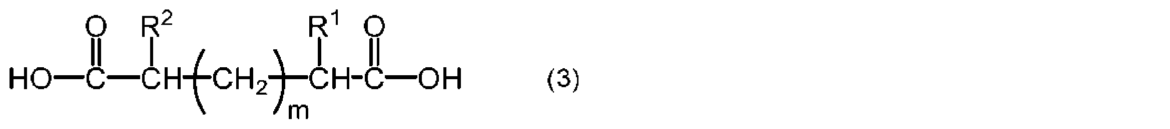
式(3)中、R1及びR2は、それぞれ独立して、水素原子又は電子供与性基を示し、mは0又は1以上の整数を示す。 In formula (3), R 1 and R 2 each independently represent a hydrogen atom or an electron-donating group, and m represents 0 or an integer of 1 or more.
式(3)におけるmは、10以下であることが好ましく、5以下であることがより好ましく、3以下であることがさらに好ましい。mが10以下であると、一層優れた接続信頼性が得られる。 In formula (3), m is preferably 10 or less, more preferably 5 or less, and even more preferably 3 or less. When m is 10 or less, even better connection reliability can be obtained.
式(3)において、R1及びR2は、水素原子であっても電子供与性基であってもよい。一層優れた接続信頼性が得られる観点から、R1及びR2の少なくとも一方は電子供与性基であることが好ましい。R1が電子供与性基であり、R2が水素原子であると、融点が低くなる傾向があり、半導体装置の接続信頼性をより向上させることができる場合がある。また、R1とR2とが異なる電子供与性基であると、R1とR2とが同じ電子供与性基である場合と比較して、融点が低くなる傾向があり、半導体装置の接続信頼性をより向上させることができる場合がある。 In formula (3), R 1 and R 2 may be a hydrogen atom or an electron-donating group. From the viewpoint of obtaining even better connection reliability, it is preferable that at least one of R 1 and R 2 is an electron-donating group. When R 1 is an electron-donating group and R 2 is a hydrogen atom, the melting point tends to be lower, and the connection reliability of the semiconductor device may be further improved. In addition, when R 1 and R 2 are different electron-donating groups, the melting point tends to be lower than when R 1 and R 2 are the same electron-donating group, and the connection reliability of the semiconductor device may be further improved.
なお、式(3)において、R1とR2とが同じ電子供与性基であると、対称構造となり融点が高くなる傾向があるが、この場合でも本発明の効果は十分に得られる。特に融点が150℃以下と十分に低い場合には、R1とR2とが同じ基であっても、R1とR2とが異なる基である場合と同程度の接続信頼性が得られる。 In addition, in formula (3), when R1 and R2 are the same electron donating group, the structure becomes symmetrical and the melting point tends to be high, but even in this case, the effect of the present invention can be sufficiently obtained. In particular, when the melting point is sufficiently low, 150°C or less, even if R1 and R2 are the same group, the same level of connection reliability can be obtained as when R1 and R2 are different groups.
フラックス化合物としては、例えば、コハク酸、グルタル酸、アジピン酸、ピメリン酸、スベリン酸、アゼライン酸、セバシン酸、ウンデカン二酸及びドデカン二酸から選択されるジカルボン酸、並びに、これらのジカルボン酸の2位に電子供与性基が置換した化合物を用いることができる。 As the flux compound, for example, a dicarboxylic acid selected from succinic acid, glutaric acid, adipic acid, pimelic acid, suberic acid, azelaic acid, sebacic acid, undecanedioic acid, and dodecanedioic acid, as well as compounds in which an electron donating group is substituted at the 2-position of these dicarboxylic acids, can be used.
フラックス化合物の融点は、150℃以下が好ましく、140℃以下がより好ましく、130℃以下がさらに好ましい。このようなフラックス化合物は、エポキシ樹脂と硬化剤との硬化反応が生じる前にフラックス活性が十分に発現しやすい。そのため、このようなフラックス化合物を含有する第1の接着剤を用いた半導体用フィルム状接着剤によれば、接続信頼性に一層優れる半導体装置を実現できる。また、フラックス化合物の融点は、25℃以上が好ましく、50℃以上がより好ましい。また、フラックス化合物は、室温(25℃)で固形であるものが好ましい。 The melting point of the flux compound is preferably 150°C or less, more preferably 140°C or less, and even more preferably 130°C or less. Such a flux compound is likely to fully exhibit flux activity before the curing reaction between the epoxy resin and the curing agent occurs. Therefore, a semiconductor device with even better connection reliability can be realized by using a film-like adhesive for semiconductors that uses a first adhesive containing such a flux compound. The melting point of the flux compound is preferably 25°C or more, and more preferably 50°C or more. The flux compound is preferably solid at room temperature (25°C).
フラックス化合物の融点は、一般的な融点測定装置を用いて測定できる。融点を測定する試料は、微粉末に粉砕され且つ微量を用いることで試料内の温度の偏差を少なくすることが求められる。試料の容器としては一方の端を閉じた毛細管が用いられることが多いが、測定装置によっては2枚の顕微鏡用カバーグラスに挟み込んで容器とするものもある。また急激に温度を上昇させると試料と温度計との間に温度勾配が発生して測定誤差を生じるため融点を計測する時点での加温は毎分1℃以下の上昇率で測定することが望ましい。 The melting point of a flux compound can be measured using a general melting point measurement device. The sample for which the melting point is to be measured is crushed into a fine powder, and a small amount is used to minimize temperature deviation within the sample. A capillary tube with one end closed is often used as a container for the sample, but some measurement devices use a container sandwiched between two microscope cover glasses. Also, if the temperature is increased suddenly, a temperature gradient will occur between the sample and the thermometer, resulting in measurement errors, so it is desirable to increase the temperature at the time of measuring the melting point at a rate of less than 1°C per minute.
前述のように融点を測定する資料は微粉末として調製されるので、融解前の試料は表面での乱反射により不透明である。試料の外見が透明化し始めた温度を融点の下限点とし、融解しきった温度を上限点とすることが通常である。測定装置は種々の形態のものが存在するが、最も古典的な装置は二重管式温度計に試料を詰めた毛細管を取り付けて温浴で加温する装置が使用される。二重管式温度計に毛細管を貼り付ける目的で温浴の液体として粘性の高い液体が用いられ、濃硫酸ないしはシリコンオイルが用いられることが多く、温度計先端の溜めの近傍に試料が来るように取り付ける。また、融点測定装置としては金属のヒートブロックを使って加温し、光の透過率を測定しながら加温を調製しつつ自動的に融点を決定するものを使用することもできる。 As mentioned above, the material for measuring the melting point is prepared as a fine powder, so the sample is opaque before melting due to diffuse reflection from the surface. The temperature at which the sample begins to become transparent is usually taken as the lower limit of the melting point, and the temperature at which it is completely melted is usually taken as the upper limit. There are various types of measuring devices, but the most classic device is a device that attaches a capillary tube filled with the sample to a double-tube thermometer and heats it in a hot bath. A highly viscous liquid is used as the hot bath liquid in order to attach the capillary tube to the double-tube thermometer, and concentrated sulfuric acid or silicone oil is often used, and the sample is attached so that it is close to the reservoir at the tip of the thermometer. In addition, a melting point measuring device can also be used that uses a metal heat block for heating, and automatically determines the melting point by adjusting the heating while measuring the light transmittance.
なお、本明細書中、融点が150℃以下とは、融点の上限点が150℃以下であることを意味し、融点が25℃以上とは、融点の下限点が25℃以上であることを意味する。 In this specification, a melting point of 150°C or less means that the upper limit of the melting point is 150°C or less, and a melting point of 25°C or more means that the lower limit of the melting point is 25°C or more.
(c)成分の含有量は、第1の接着剤の全量基準で、0.5~10質量%であることが好ましく、0.5~5質量%であることがより好ましい。 The content of component (c) is preferably 0.5 to 10 mass % based on the total amount of the first adhesive, and more preferably 0.5 to 5 mass %.
[(d)成分:重量平均分子量が10000以上の高分子成分]
第1の接着剤は、必要に応じて、重量平均分子量が10000以上の高分子成分((d)成分)を含有していてもよい。(d)成分を含有する第1の接着剤は、耐熱性及びフィルム形成性に一層優れる。
[Component (d): Polymer component having a weight average molecular weight of 10,000 or more]
The first adhesive may, as necessary, contain a polymer component (component (d)) having a weight average molecular weight of at least 10,000. A first adhesive containing component (d) has even more excellent heat resistance and film formability.
(d)成分としては、例えば、フェノキシ樹脂、ポリイミド樹脂、ポリアミド樹脂、ポリカルボジイミド樹脂、シアネートエステル樹脂、アクリル樹脂、ポリエステル樹脂、ポリエチレン樹脂、ポリエーテルスルホン樹脂、ポリエーテルイミド樹脂、ポリビニルアセタール樹脂、ウレタン樹脂及びアクリルゴムが挙げられる。これらの中でも耐熱性及びフィルム形成性に優れる観点から、フェノキシ樹脂、ポリイミド樹脂、アクリルゴム、シアネートエステル樹脂及びポリカルボジイミド樹脂が好ましく、フェノキシ樹脂、ポリイミド樹脂及びアクリルゴムがより好ましい。これらの(d)成分は単独で又は2種以上の混合物又は共重合体として使用することもできる。ただし、(d)成分には、(a)成分に該当する化合物及び(e)成分に該当する化合物は含まれない。 Examples of the (d) component include phenoxy resin, polyimide resin, polyamide resin, polycarbodiimide resin, cyanate ester resin, acrylic resin, polyester resin, polyethylene resin, polyethersulfone resin, polyetherimide resin, polyvinyl acetal resin, urethane resin, and acrylic rubber. Among these, from the viewpoint of excellent heat resistance and film formability, phenoxy resin, polyimide resin, acrylic rubber, cyanate ester resin, and polycarbodiimide resin are preferred, and phenoxy resin, polyimide resin, and acrylic rubber are more preferred. These (d) components can be used alone or as a mixture or copolymer of two or more kinds. However, the (d) component does not include a compound corresponding to the (a) component or a compound corresponding to the (e) component.
(d)成分の重量平均分子量は、例えば10000以上であり、20000以上であることが好ましく、30000以上であることがより好ましい。このような(d)成分によれば、第1の接着剤の耐熱性及びフィルム形成性を一層向上させることができる。 The weight average molecular weight of component (d) is, for example, 10,000 or more, preferably 20,000 or more, and more preferably 30,000 or more. Such component (d) can further improve the heat resistance and film formability of the first adhesive.
また、(d)成分の重量平均分子量は、1000000以下であることが好ましく、500000以下であることがより好ましい。このような(d)成分によれば、第1の接着剤の耐熱性を一層向上させることができる。 The weight average molecular weight of component (d) is preferably 1,000,000 or less, and more preferably 500,000 or less. Such component (d) can further improve the heat resistance of the first adhesive.
なお、本明細書において、重量平均分子量とは、高速液体クロマトグラフィー(株式会社島津製作所製、商品名:C-R4A)を用いて、ポリスチレン換算で測定したときの重量平均分子量を意味する。測定には、例えば、下記の条件を用いることができる。
検出器:LV4000 UV Detector(株式会社日立製作所製、商品名)
ポンプ:L6000 Pump(株式会社日立製作所製、商品名)
カラム:Gelpack GL-S300MDT-5(計2本)(日立化成株式会社製、商品名)
溶離液:THF/DMF=1/1(容積比)+LiBr(0.03mol/L)+H3PO4(0.06mol/L)
流量:1mL/分
In this specification, the weight average molecular weight means a weight average molecular weight measured in terms of polystyrene using high performance liquid chromatography (manufactured by Shimadzu Corporation, product name: C-R4A). For example, the following conditions can be used for the measurement.
Detector: LV4000 UV Detector (product name, manufactured by Hitachi, Ltd.)
Pump: L6000 Pump (product name, manufactured by Hitachi, Ltd.)
Column: Gelpack GL-S300MDT-5 (total of 2 columns) (manufactured by Hitachi Chemical Co., Ltd., product name)
Eluent: THF/DMF=1/1 (volume ratio) + LiBr (0.03 mol/L) + H3PO4 (0.06 mol/L)
Flow rate: 1 mL/min
第1の接着剤が(d)成分を含有するとき、(d)成分の含有量Cdに対する(a)成分の含有量Caの比Ca/Cd(質量比)は、0.01~5であることが好ましく、0.05~3であることがより好ましく、0.1~2であることがさらに好ましい。比Ca/Cdを0.01以上とすることで、より良好な硬化性及び接着力が得られ、比Ca/Cdを5以下とすることでより良好なフィルム形成性が得られる。 When the first adhesive contains the component (d), the ratio C a /C d (mass ratio) of the content C a of the component (a) to the content C d of the component (d) is preferably 0.01 to 5, more preferably 0.05 to 3, and even more preferably 0.1 to 2. By setting the ratio C a /C d to 0.01 or more, better curing properties and adhesive strength can be obtained, and by setting the ratio C a /C d to 5 or less, better film formability can be obtained.
[(e)成分:フィラー]
第1の接着剤は、必要に応じて、フィラー((e)成分)を含有していてもよい。(e)成分によって、第1の接着剤の粘度、第1の接着剤の硬化物の物性等を制御することができる。具体的には、(e)成分によれば、例えば、接続時のボイド発生の抑制、第1の接着剤の硬化物の吸湿率の低減等を図ることができる。
[Component (e): Filler]
The first adhesive may contain a filler (component (e)) as necessary. The component (e) can control the viscosity of the first adhesive, the physical properties of the cured product of the first adhesive, and the like. Specifically, the component (e) can, for example, suppress the generation of voids during connection, reduce the moisture absorption rate of the cured product of the first adhesive, and the like.
(e)成分としては、無機フィラー(無機粒子)、有機フィラー(有機粒子)等が挙げられる。無機フィラーとしては、ガラス、シリカ、アルミナ、酸化チタン、マイカ、窒化ホウ素等の絶縁性無機フィラーが挙げられ、その中でも、シリカ、アルミナ、酸化チタン及び窒化ホウ素からなる群より選ばれる少なくとも1種が好ましく、シリカ、アルミナ及び窒化ホウ素からなる群より選ばれる少なくとも1種がより好ましい。絶縁性無機フィラーはウィスカーであってもよい。ウィスカーとしては、ホウ酸アルミニウム、チタン酸アルミニウム、酸化亜鉛、珪酸カルシウム、窒化ホウ素等が挙げられる。有機フィラーとしては、例えば、樹脂フィラー(樹脂粒子)が挙げられる。樹脂フィラーとしては、ポリウレタン、ポリイミド等が挙げられる。樹脂フィラーは、無機フィラーに比べて、260℃等の高温で柔軟性を付与することができるため、耐リフロー性向上に適していると共に、柔軟性付与が可能であるためフィルム形成性向上にも効果がある。 Component (e) includes inorganic fillers (inorganic particles), organic fillers (organic particles), etc. Inorganic fillers include insulating inorganic fillers such as glass, silica, alumina, titanium oxide, mica, and boron nitride, among which at least one selected from the group consisting of silica, alumina, titanium oxide, and boron nitride is preferred, and at least one selected from the group consisting of silica, alumina, and boron nitride is more preferred. The insulating inorganic filler may be whiskers. Examples of whiskers include aluminum borate, aluminum titanate, zinc oxide, calcium silicate, and boron nitride. Examples of organic fillers include resin fillers (resin particles). Examples of resin fillers include polyurethane and polyimide. Compared to inorganic fillers, resin fillers can impart flexibility at high temperatures such as 260°C, making them suitable for improving reflow resistance, and they are also effective in improving film formability because they can impart flexibility.
絶縁信頼性に更に優れる観点から、(e)成分は絶縁性であることが好ましい。第1の接着剤は、銀フィラー、はんだフィラー等の導電性の金属フィラー(金属粒子)、及び、カーボンブラック等の導電性の無機フィラーを含有していないことが好ましい。 From the viewpoint of further improving insulation reliability, it is preferable that component (e) is insulating. It is preferable that the first adhesive does not contain conductive metal fillers (metal particles) such as silver fillers and solder fillers, and conductive inorganic fillers such as carbon black.
(e)成分の物性は、表面処理によって適宜調整されてもよい。(e)成分は、分散性又は接着力が向上する観点から、表面処理を施したフィラーであることが好ましい。表面処理剤としては、グリシジル系(エポキシ系)、アミン系、フェニル系、フェニルアミノ系、(メタ)アクリル系、ビニル系の化合物等が挙げられる。 The physical properties of component (e) may be adjusted as appropriate by surface treatment. From the viewpoint of improving dispersibility or adhesive strength, component (e) is preferably a filler that has been surface-treated. Examples of surface treatment agents include glycidyl-based (epoxy-based), amine-based, phenyl-based, phenylamino-based, (meth)acrylic-based, and vinyl-based compounds.
表面処理としては、表面処理のしやすさから、エポキシシラン系、アミノシラン系、アクリルシラン系等のシラン化合物によるシラン処理が好ましい。表面処理剤としては、分散性、流動性及び接着力に優れる観点から、グリシジル系の化合物、フェニルアミノ系の化合物、及び、(メタ)アクリル系の化合物からなる群より選ばれる少なくとも1種が好ましい。表面処理剤としては、保存安定性に優れる観点から、フェニル系の化合物、及び、(メタ)アクリル系の化合物からなる群より選ばれる少なくとも1種が好ましい。 As the surface treatment, silane treatment using a silane compound such as an epoxy silane, amino silane, or acrylic silane is preferred because of the ease of surface treatment. As the surface treatment agent, from the viewpoint of excellent dispersibility, fluidity, and adhesive strength, at least one selected from the group consisting of a glycidyl compound, a phenylamino compound, and a (meth)acrylic compound is preferred. As the surface treatment agent, from the viewpoint of excellent storage stability, at least one selected from the group consisting of a phenyl compound and a (meth)acrylic compound is preferred.
(e)成分の平均粒径は、フリップチップ接続時のかみ込み防止の観点から、1.5μm以下が好ましく、視認性(透明性)に優れる観点から、1.0μm以下がより好ましい。 The average particle size of component (e) is preferably 1.5 μm or less from the viewpoint of preventing jamming during flip chip connection, and more preferably 1.0 μm or less from the viewpoint of excellent visibility (transparency).
(e)成分の含有量は、放熱性が低くなることが抑制される観点、及び、ボイドの発生、吸湿率が大きくなること等を抑制しやすい傾向がある観点から、第1の接着剤の全量を基準として、30質量%以上が好ましく、40質量%以上がより好ましい。(e)成分の含有量は、粘度が高くなって第1の接着剤の流動性が低下すること、及び、接続部へのフィラーの噛み込み(トラッピング)が生じることが抑制されやすく、接続信頼性が低下することを抑制しやすい傾向がある観点から、第1の接着剤の全量を基準として、90質量%以下が好ましく、80質量%以下がより好ましい。これらの観点から、(e)成分の含有量は、第1の接着剤の全量を基準として、30~90質量%が好ましく、40~80質量%がより好ましい。 The content of the (e) component is preferably 30% by mass or more, and more preferably 40% by mass or more, based on the total amount of the first adhesive, from the viewpoint of suppressing a decrease in heat dissipation and a tendency to easily suppress the occurrence of voids and an increase in moisture absorption rate. The content of the (e) component is preferably 90% by mass or less, and more preferably 80% by mass or less, based on the total amount of the first adhesive, from the viewpoint of easily suppressing an increase in viscosity and a decrease in the fluidity of the first adhesive, and of easily suppressing the occurrence of filler trapping in the connection portion, and of easily suppressing a decrease in connection reliability. From these viewpoints, the content of the (e) component is preferably 30 to 90% by mass, and more preferably 40 to 80% by mass, based on the total amount of the first adhesive.
[その他の成分]
第1の接着剤には、酸化防止剤、シランカップリング剤、チタンカップリング剤、レベリング剤、イオントラップ剤等の添加剤を配合してもよい。これらは1種を単独で又は2種以上を組み合わせて用いることができる。これらの配合量については、各添加剤の効果が発現するように適宜調整すればよい。
[Other ingredients]
The first adhesive may contain additives such as an antioxidant, a silane coupling agent, a titanium coupling agent, a leveling agent, and an ion trapping agent. These may be used alone or in combination of two or more. The amount of each additive may be appropriately adjusted so that the effect of each additive is exerted.
(第2の接着剤)
第2の接着剤は、フラックス化合物を実質的に含有しない。「実質的に含有しない」とは、第2の接着剤におけるフラックス化合物の含有量が、第2の接着剤の全量基準で、0.5質量%未満であることを意味する。
(Second Adhesive)
The second adhesive is substantially free of a flux compound. "Substantially free of" means that the content of the flux compound in the second adhesive is less than 0.5 mass % based on the total amount of the second adhesive.
第2の接着剤は、本発明の効果が顕著に得られる観点から、200℃で5秒間保持したときの硬化反応率が80%以上であることが好ましい。このような第2の接着剤としては、例えば、ラジカル硬化系の接着剤が挙げられる。このような接着剤により本発明の効果が顕著に得られる理由は、明らかではないが、本発明者らは次のように推察している。 From the viewpoint of obtaining a remarkable effect of the present invention, it is preferable that the second adhesive has a curing reaction rate of 80% or more when held at 200°C for 5 seconds. An example of such a second adhesive is a radical curing adhesive. The reason why such an adhesive provides a remarkable effect of the present invention is not clear, but the inventors speculate as follows.
すなわち、従来のフラックス化合物を含有するフィルム状接着剤では、フラックス成分がラジカルを失活させてしまうため、ラジカル硬化系を適用することができず、エポキシ等を用いたカチオン硬化系が適用されることが多かった。この硬化系(反応系)では、求核付加反応で硬化が進行するため、硬化速度が遅く、圧着後にボイドが発生してしまう場合があった。従来のフィルム状接着剤では、この実装時のボイドによって、不具合(例えば260℃前後のリフロー温度における半導体材料の剥離、接続部の接続不良等)が発生していたと推察される。一方、上述の第2の接着剤は、フラックス化合物を実質的に含有していないために、硬化系をラジカル硬化系とすることができ、充分な硬化速度を得ることができる。そのため、上述の第2の接着剤を第2の層に用いることで、圧着を高温且つ短時間で行った場合であってもボイドが発生し難くなり、本発明の効果が顕著となると推察される。また、本実施形態では、充分な硬化速度を得ることができることから、例えば、接続部にはんだが用いられている場合であっても、はんだ溶融温度より低温の温度領域でフィルム状接着剤を硬化させることができる。そのため、はんだの飛散及び流動が発生して接続不良が生じることを充分に抑制できる。 That is, in the conventional film-like adhesive containing a flux compound, the flux component deactivates the radicals, so that a radical curing system cannot be applied, and a cationic curing system using epoxy or the like is often applied. In this curing system (reaction system), the curing proceeds by a nucleophilic addition reaction, so the curing speed is slow, and voids may occur after compression. In the conventional film-like adhesive, it is presumed that the voids during mounting caused problems (for example, peeling of the semiconductor material at a reflow temperature of about 260 ° C, poor connection of the connection part, etc.). On the other hand, since the above-mentioned second adhesive does not substantially contain a flux compound, the curing system can be a radical curing system, and a sufficient curing speed can be obtained. Therefore, it is presumed that by using the above-mentioned second adhesive in the second layer, voids are unlikely to occur even when compression is performed at a high temperature and for a short time, and the effect of the present invention is remarkable. In addition, in this embodiment, since a sufficient curing speed can be obtained, for example, even when solder is used in the connection part, the film-like adhesive can be cured in a temperature range lower than the solder melting temperature. This effectively prevents solder from scattering or flowing, which can lead to poor connections.
以下、第2の接着剤が、ラジカル重合性化合物(以下、場合により「(A)成分」という。)と、熱ラジカル発生剤(以下、場合により「(B)成分」という。)と、必要に応じて、高分子成分(以下、場合により「(C)成分」という。)及びフィラー(以下、場合により「(D)成分」という。)と、を含有する一実施形態について説明する。 Hereinafter, an embodiment will be described in which the second adhesive contains a radical polymerizable compound (hereinafter, sometimes referred to as "component (A)"), a thermal radical generator (hereinafter, sometimes referred to as "component (B)"), and, if necessary, a polymer component (hereinafter, sometimes referred to as "component (C)") and a filler (hereinafter, sometimes referred to as "component (D)").
[(A)成分:ラジカル重合性化合物]
(A)成分は、熱、光、放射線、及び、電気化学的作用などによるラジカルの発生に伴い、ラジカル重合反応が可能である化合物である。(A)成分としては、(メタ)アクリル化合物、ビニル化合物等が挙げられる。(A)成分としては、耐久性、電気絶縁性及び耐熱性に優れる観点から、(メタ)アクリル化合物が好ましい。(メタ)アクリル化合物は、分子内に1個以上の(メタ)アクリル基((メタ)アクリロイル基)を有する化合物であれば特に制限はなく、例えば、ビスフェノールA型、ビスフェノールF型、ナフタレン型、フェノールノボラック型、クレゾールノボラック型、フェノールアラルキル型、ビフェニル型、トリフェニルメタン型、ジシクロペンタジエン型、フルオレン型、アダマンタン型又はイソシアヌル酸型の骨格を含有する(メタ)アクリル化合物;各種多官能(メタ)アクリル化合物(前記骨格を含有する(メタ)アクリル化合物を除く)等を使用することができる。多官能(メタ)アクリル化合物としては、ペンタエリスリトールトリ(メタ)アクリレート、ジペンタエリスリトールペンタ(メタ)アクリレート、トリメチロールプロパンジ(メタ)アクリレート等が挙げられる。(A)成分は、1種単独で又は2種以上を併用して用いることができる。
[Component (A): radically polymerizable compound]
The (A) component is a compound capable of radical polymerization reaction with the generation of radicals by heat, light, radiation, electrochemical action, etc. Examples of the (A) component include (meth)acrylic compounds and vinyl compounds. As the (A) component, a (meth)acrylic compound is preferable from the viewpoint of excellent durability, electrical insulation, and heat resistance. The (meth)acrylic compound is not particularly limited as long as it is a compound having one or more (meth)acrylic groups ((meth)acryloyl groups) in the molecule, and for example, (meth)acrylic compounds containing a bisphenol A type, bisphenol F type, naphthalene type, phenol novolac type, cresol novolac type, phenol aralkyl type, biphenyl type, triphenylmethane type, dicyclopentadiene type, fluorene type, adamantane type, or isocyanuric acid type skeleton; various polyfunctional (meth)acrylic compounds (excluding (meth)acrylic compounds containing the skeleton) and the like can be used. Examples of polyfunctional (meth)acrylic compounds include pentaerythritol tri(meth)acrylate, dipentaerythritol penta(meth)acrylate, trimethylolpropane di(meth)acrylate, etc. The component (A) may be used alone or in combination of two or more.
(A)成分は、耐熱性に優れる観点から、ビスフェノールA型骨格、ビスフェノールF型骨格、ナフタレン型骨格、フルオレン型骨格、アダマンタン型骨格又はイソシアヌル酸型骨格を有することが好ましく、フルオレン型骨格を有することがより好ましい。(A)成分は、上述したいずれかの骨格を有する(メタ)アクリレートであることが更に好ましい。 From the viewpoint of excellent heat resistance, the (A) component preferably has a bisphenol A type skeleton, a bisphenol F type skeleton, a naphthalene type skeleton, a fluorene type skeleton, an adamantane type skeleton, or an isocyanuric acid type skeleton, and more preferably has a fluorene type skeleton. It is even more preferable that the (A) component is a (meth)acrylate having any of the above skeletons.
(A)成分は、室温(25℃)で固形であることが好ましい。液状に比べて固形の方が、ボイドが発生しにくく、また、硬化前(Bステージ)の第2の接着剤の粘性(タック)が小さく取り扱い性に優れる。室温(25℃)で固形である(A)成分としては、ビスフェノールA型骨格、フルオレン型骨格、アダマンタン型骨格、又はイソシアヌル酸型骨格を有する(メタ)アクリレート等が挙げられる。 Component (A) is preferably solid at room temperature (25°C). A solid state is less likely to cause voids than a liquid state, and the second adhesive has less viscosity (tack) before curing (B stage), making it easier to handle. Examples of component (A) that is solid at room temperature (25°C) include (meth)acrylates having a bisphenol A type skeleton, a fluorene type skeleton, an adamantane type skeleton, or an isocyanuric acid type skeleton.
(A)成分における(メタ)アクリル基の官能基数は、3以下が好ましい。官能基数が多い場合、硬化のネットワークが急速に進み、未反応基が残存する場合がある。一方、官能基数が3以下であると、官能基数が多くなりすぎず、短時間での硬化が充分に進行しやすいため、硬化反応率が低下することを抑制しやすい。 The number of functional groups of the (meth)acrylic group in component (A) is preferably 3 or less. If the number of functional groups is large, the curing network may progress too quickly, and unreacted groups may remain. On the other hand, if the number of functional groups is 3 or less, the number of functional groups is not too large, and curing can easily proceed sufficiently in a short period of time, making it easier to prevent a decrease in the curing reaction rate.
(A)成分の分子量は、2000より小さいことが好ましく、1000以下であることがより好ましい。(A)成分の分子量が小さいほど反応が進行しやすく、硬化反応率が高くなる。 The molecular weight of component (A) is preferably less than 2000, and more preferably less than 1000. The smaller the molecular weight of component (A), the easier the reaction will proceed and the higher the curing reaction rate will be.
(A)成分の含有量は、硬化成分が少なくなることが抑制され、硬化後の樹脂の流動を充分に制御しやすい観点から、第2の接着剤の全量を基準として、10質量%以上が好ましく、15質量%以上がより好ましい。(A)成分の含有量は、硬化物が硬くなりすぎることが抑制され、パッケージの反りが大きくなることが抑制されやすい傾向がある観点から、第2の接着剤の全量を基準として、50質量%以下が好ましく、40質量%以下がより好ましい。これらの観点から、(A)成分の含有量は、第2の接着剤の全量を基準として、10~50質量%が好ましく、15~40質量%がより好ましい。 The content of component (A) is preferably 10% by mass or more, and more preferably 15% by mass or more, based on the total amount of the second adhesive, from the viewpoint of preventing the cured component from becoming too hard and making it easy to sufficiently control the flow of the resin after curing. The content of component (A) is preferably 50% by mass or less, and more preferably 40% by mass or less, based on the total amount of the second adhesive, from the viewpoint of preventing the cured product from becoming too hard and making it easy to prevent the package from warping too much. From these viewpoints, the content of component (A) is preferably 10 to 50% by mass, and more preferably 15 to 40% by mass, based on the total amount of the second adhesive.
(A)成分の含有量は、硬化性が低下することが抑制され、接着力が低下することが抑制されやすい観点から、(C)成分1質量部に対して、0.01質量部以上が好ましく、0.05質量部以上がより好ましく、0.1質量部以上が更に好ましい。(A)成分の含有量は、フィルム形成性が低下することが抑制されやすい観点から、(C)成分1質量部に対して、10質量部以下が好ましく、5質量部以下がより好ましい。これらの観点から、(A)成分の含有量は、(C)成分1質量部に対して、0.01~10質量部が好ましく、0.05~5質量部がより好ましく、0.1~5質量部が更に好ましい。 The content of the (A) component is preferably 0.01 parts by mass or more, more preferably 0.05 parts by mass or more, and even more preferably 0.1 parts by mass or more, per 1 part by mass of the (C) component, from the viewpoint of easily suppressing a decrease in curability and a decrease in adhesive strength. The content of the (A) component is preferably 10 parts by mass or less, more preferably 5 parts by mass or less, per 1 part by mass of the (C) component, from the viewpoint of easily suppressing a decrease in film formability. From these viewpoints, the content of the (A) component is preferably 0.01 to 10 parts by mass, more preferably 0.05 to 5 parts by mass, and even more preferably 0.1 to 5 parts by mass, per 1 part by mass of the (C) component.
[(B)成分:熱ラジカル発生剤]
(B)成分としては、(A)成分の硬化剤として機能すれば特に制限はないが、取り扱い性に優れる観点から、熱ラジカル発生剤が好ましい。
[Component (B): Thermal Radical Generator]
There are no particular limitations on the component (B) as long as it functions as a curing agent for the component (A), but from the standpoint of excellent handleability, a thermal radical generator is preferred.
熱ラジカル発生剤としては、アゾ化合物、過酸化物(有機過酸化物等)などが挙げられる。熱ラジカル発生剤としては、過酸化物が好ましく、有機過酸化物がより好ましい。この場合、フィルム形態にする際の溶剤を乾燥させる工程でラジカル反応が進行せず、取り扱い性及び保存安定性に優れる。そのため、熱ラジカル発生剤として過酸化物を用いる場合、一層優れた接続信頼性が得られやすい。有機過酸化物としては、ケトンパーオキサイド、パーオキシケタール、ハイドロパーオキサイド、ジアルキルパーオキサイド、ジアシルパーオキサイド、パーオキシジカーボネイト、パーオキシエステル等が挙げられる。有機過酸化物としては、保存安定性に優れる観点から、ハイドロパーオキサイド、ジアルキルパーオキサイド及びパーオキシエステルからなる群より選ばれる少なくとも1種が好ましい。さらに、有機過酸化物としては、耐熱性に優れる観点から、ハイドロパーオキサイド及びジアルキルパーオキサイドからなる群より選ばれる少なくとも1種が好ましい。ジアルキルパーオキサイドとしては、ジクミル過酸化物、ジ-tert-ブチル過酸化物等が挙げられる。 Examples of the thermal radical generator include azo compounds and peroxides (organic peroxides, etc.). As the thermal radical generator, peroxides are preferred, and organic peroxides are more preferred. In this case, radical reactions do not proceed during the process of drying the solvent when forming the film, and handling and storage stability are excellent. Therefore, when peroxides are used as the thermal radical generator, it is easy to obtain even better connection reliability. Examples of the organic peroxides include ketone peroxides, peroxyketals, hydroperoxides, dialkyl peroxides, diacyl peroxides, peroxydicarbonates, peroxyesters, etc. From the viewpoint of excellent storage stability, at least one organic peroxide selected from the group consisting of hydroperoxides, dialkyl peroxides, and peroxyesters is preferred. Furthermore, from the viewpoint of excellent heat resistance, at least one organic peroxide selected from the group consisting of hydroperoxides and dialkyl peroxides is preferred. Examples of the dialkyl peroxides include dicumyl peroxide and di-tert-butyl peroxide.
(B)成分の含有量は、充分に硬化が進行しやすい観点から、(A)成分100質量部に対して、0.5質量部以上が好ましく、1質量部以上がより好ましい。(B)成分の含有量は、(A)成分100質量部に対して、10質量部以下が好ましく、5質量部以下がより好ましい。(B)成分の含有量の上限値が上記範囲であると、硬化が急激に進行して反応点が多くなることが抑制されることにより、分子鎖が短くなること、及び、未反応基が残存することが抑制される。そのため、(B)成分の含有量の上限値が上記範囲であると、信頼性の低下を抑制しやすい傾向がある。これらの観点から、(B)成分の含有量は、(A)成分100質量部に対して、0.5~10質量部が好ましく、1~5質量部がより好ましい。 From the viewpoint of sufficient curing, the content of the (B) component is preferably 0.5 parts by mass or more, and more preferably 1 part by mass or more, per 100 parts by mass of the (A) component. The content of the (B) component is preferably 10 parts by mass or less, and more preferably 5 parts by mass or less, per 100 parts by mass of the (A) component. When the upper limit of the (B) component content is within the above range, the curing is prevented from progressing too rapidly and the number of reaction points is increased, thereby preventing the molecular chain from becoming shorter and preventing unreacted groups from remaining. Therefore, when the upper limit of the (B) component content is within the above range, there is a tendency to easily prevent a decrease in reliability. From these viewpoints, the content of the (B) component is preferably 0.5 to 10 parts by mass, and more preferably 1 to 5 parts by mass, per 100 parts by mass of the (A) component.
[(C)成分:高分子成分]
第2の接着剤は、高分子成分を更に含有することができる。(C)成分は、エポキシ樹脂、フェノキシ樹脂、ポリイミド樹脂、ポリアミド樹脂、ポリカルボジイミド樹脂、シアネートエステル樹脂、(メタ)アクリル樹脂、ポリエステル樹脂、ポリエチレン樹脂、ポリエーテルスルホン樹脂、ポリエーテルイミド樹脂、ポリビニルアセタール樹脂、ウレタン樹脂、アクリルゴム等が挙げられ、その中でも、耐熱性及びフィルム形成性に優れる観点から、エポキシ樹脂、フェノキシ樹脂、ポリイミド樹脂、(メタ)アクリル樹脂、アクリルゴム、シアネートエステル樹脂及びポリカルボジイミド樹脂からなる群より選ばれる少なくとも1種が好ましく、エポキシ樹脂、フェノキシ樹脂、ポリイミド樹脂、(メタ)アクリル樹脂及びアクリルゴムからなる群より選ばれる少なくとも1種がより好ましい。(C)成分は、1種単独又は2種以上の混合体又は共重合体として使用することもできる。ただし、(C)成分には、(A)成分に該当する化合物、及び、(D)成分に該当する化合物は含まれない。
[(C) component: polymer component]
The second adhesive may further contain a polymer component. The component (C) may be an epoxy resin, a phenoxy resin, a polyimide resin, a polyamide resin, a polycarbodiimide resin, a cyanate ester resin, a (meth)acrylic resin, Examples of the resin include polyester resin, polyethylene resin, polyethersulfone resin, polyetherimide resin, polyvinyl acetal resin, urethane resin, and acrylic rubber. Among these, epoxy resin, phenoxy resin, and the like are preferred from the viewpoint of excellent heat resistance and film formability. At least one selected from the group consisting of polyimide resin, (meth)acrylic resin, acrylic rubber, cyanate ester resin, and polycarbodiimide resin is preferred, and at least one selected from the group consisting of epoxy resin, phenoxy resin, polyimide resin, (meth)acrylic resin, and acrylic rubber is preferred. It is more preferable to use at least one selected from the group consisting of (A) and (B). The component (C) may be used alone or as a mixture or copolymer of two or more kinds. However, the component (C) may contain at least one of the following: This does not include compounds corresponding to component (A) and compounds corresponding to component (D).
(C)成分のガラス転移温度(Tg)は、半導体用フィルム状接着剤の基板又はチップへの貼付性に優れる観点から、120℃以下が好ましく、100℃以下がより好ましく、85℃以下が更に好ましい。これらの範囲である場合には、半導体チップに形成されたバンプ、基板に形成された電極又は配線パターン等の凹凸を半導体用フィルム状接着剤により容易に埋め込むことが可能であり(硬化反応が始まることを抑制しやすい)、気泡が残存してボイドが発生することを抑制しやすい傾向がある。なお、上記Tgとは、DSC(パーキンエルマー社製、商品名:DSC-7型)を用いて、サンプル量10mg、昇温速度10℃/分、測定雰囲気:空気の条件で測定したときのTgである。 The glass transition temperature (Tg) of component (C) is preferably 120°C or less, more preferably 100°C or less, and even more preferably 85°C or less, from the viewpoint of excellent adhesion of the film-like adhesive for semiconductors to the substrate or chip. When it is within these ranges, it is possible to easily fill the unevenness of bumps formed on the semiconductor chip, electrodes or wiring patterns formed on the substrate, etc. with the film-like adhesive for semiconductors (easier to suppress the start of the curing reaction), and there is a tendency to easily suppress the occurrence of voids due to residual air bubbles. The above Tg is the Tg measured using a DSC (manufactured by PerkinElmer, product name: DSC-7 type) under the conditions of a sample amount of 10 mg, a heating rate of 10°C/min, and a measurement atmosphere of air.
(C)成分の重量平均分子量は、ポリスチレン換算で10000以上が好ましく、単独で良好なフィルム形成性を示すために、30000以上がより好ましく、40000以上が更に好ましく、50000以上が特に好ましい。重量平均分子量が10000以上である場合には、フィルム形成性が低下することを抑制しやすい傾向がある。 The weight average molecular weight of component (C) is preferably 10,000 or more in terms of polystyrene, and in order to exhibit good film-forming properties alone, it is more preferably 30,000 or more, even more preferably 40,000 or more, and particularly preferably 50,000 or more. When the weight average molecular weight is 10,000 or more, there is a tendency to easily suppress a decrease in film-forming properties.
[(D)成分:フィラー]
第2の接着剤は、粘度又は硬化物の物性を制御するため、及び、半導体チップと基板、若しくは半導体チップ同士を接続した際のボイドの発生又は吸湿率の更なる抑制のために、フィラーを更に含有してもよい。(D)成分としては、第1の接着剤における(d)成分として挙げたフィラーと同様のフィラーを用いることができる。好ましいフィラーの例も同じである。
[Component (D): Filler]
The second adhesive may further contain a filler in order to control the viscosity or physical properties of the cured product, and to further suppress the generation of voids or the moisture absorption rate when connecting a semiconductor chip to a substrate or connecting semiconductor chips to each other. As the (D) component, a filler similar to the filler listed as the (d) component in the first adhesive can be used. Examples of preferred fillers are also the same.
(D)成分の含有量は、放熱性が低くなることが抑制される観点、及び、ボイドの発生、吸湿率が大きくなること等を抑制しやすい傾向がある観点から、第2の接着剤の全量を基準として、30質量%以上が好ましく、40質量%以上がより好ましい。(D)成分の含有量は、粘度が高くなって第2の接着剤の流動性が低下すること、及び、接続部へのフィラーの噛み込み(トラッピング)が生じることが抑制されやすく、接続信頼性が低下することを抑制しやすい傾向がある観点から、第2の接着剤の全量を基準として、90質量%以下が好ましく、80質量%以下がより好ましい。これらの観点から、(D)成分の含有量は、第2の接着剤の全量を基準として、30~90質量%が好ましく、40~80質量%がより好ましい。 The content of the (D) component is preferably 30% by mass or more, and more preferably 40% by mass or more, based on the total amount of the second adhesive, from the viewpoint of suppressing a decrease in heat dissipation and a tendency to easily suppress the occurrence of voids and an increase in moisture absorption rate. The content of the (D) component is preferably 90% by mass or less, and more preferably 80% by mass or less, based on the total amount of the second adhesive, from the viewpoint of easily suppressing an increase in viscosity and a decrease in the fluidity of the second adhesive, and of easily suppressing the occurrence of filler trapping in the connection portion, and of easily suppressing a decrease in connection reliability. From these viewpoints, the content of the (D) component is preferably 30 to 90% by mass, and more preferably 40 to 80% by mass, based on the total amount of the second adhesive.
[その他の成分]
第2の接着剤には、ラジカル重合性化合物以外の重合性化合物(例えば、カチオン重合性化合物及びアニオン重合性化合物)を配合してもよい。また、第2の接着剤には、第1の接着剤と同様のその他の成分を配合してもよい。これらは1種を単独で又は2種以上を組み合わせて用いることができる。これらの配合量については、各添加剤の効果が発現するように適宜調整すればよい。
[Other ingredients]
The second adhesive may contain a polymerizable compound other than the radical polymerizable compound (e.g., a cationic polymerizable compound and an anionic polymerizable compound). The second adhesive may contain other components similar to those in the first adhesive. These may be used alone or in combination of two or more. The amounts of these additives may be appropriately adjusted so that the effects of each additive are exerted.
第2の接着剤を200℃で5秒保持したときの硬化反応率は、80%以上であることが好ましく、90%以上であることがより好ましい。200℃(はんだ溶融温度以下)/5秒の硬化反応率が80%以上であれば、接続時(はんだ溶融温度以上)ではんだが飛散・流動し接続信頼性が低下することを抑制しやすい。硬化反応率は、第2の接着剤(未硬化のフラックス非含有層)10mgをアルミニウムパンに入れた後、DSC(パーキンエルマー社製、商品名:DSC-7型)を用いて発熱量を測定することにより得ることができる。具体的には、第2の接着剤(未硬化のフラックス非含有層)10mgをアルミニウムパンに入れた測定サンプルを200℃に加温したホットプレート上に置き、5秒後にホットプレート上から測定サンプルを外す。熱処理後の測定サンプルと、未処理の測定サンプルをそれぞれDSCで測定する。得られた発熱量から、下記式により硬化反応率を算出する。
硬化反応率(%)=(1-[熱処理後の測定サンプルの発熱量]/[未処理の測定サンプルの発熱量])×100
The curing reaction rate when the second adhesive is held at 200°C for 5 seconds is preferably 80% or more, more preferably 90% or more. If the curing reaction rate at 200°C (below the solder melting temperature)/5 seconds is 80% or more, it is easy to suppress the solder from scattering and flowing at the time of connection (above the solder melting temperature) and reducing the connection reliability. The curing reaction rate can be obtained by placing 10 mg of the second adhesive (uncured flux-free layer) in an aluminum pan and then measuring the amount of heat generated using a DSC (manufactured by PerkinElmer, product name: DSC-7 type). Specifically, a measurement sample in which 10 mg of the second adhesive (uncured flux-free layer) is placed in an aluminum pan is placed on a hot plate heated to 200°C, and the measurement sample is removed from the hot plate after 5 seconds. The measurement sample after the heat treatment and the untreated measurement sample are each measured by DSC. From the obtained amount of heat generated, the curing reaction rate is calculated using the following formula.
Curing reaction rate (%)=(1-[amount of heat generated from the measured sample after heat treatment]/[amount of heat generated from the untreated measured sample])×100
第2の樹脂がアニオン重合性のエポキシ樹脂(特に、重量平均分子量10000以上のエポキシ樹脂)を含有すると、硬化反応率を80%以上に調整することが難しい場合がある。エポキシ樹脂の含有量は、(A)成分80質量部に対して20質量部以下であることが好ましく、エポキシ樹脂を含有していないことがより好ましい。 If the second resin contains an anionically polymerizable epoxy resin (particularly an epoxy resin with a weight average molecular weight of 10,000 or more), it may be difficult to adjust the curing reaction rate to 80% or more. The content of the epoxy resin is preferably 20 parts by mass or less per 80 parts by mass of component (A), and it is more preferable that the second resin does not contain any epoxy resin.
第2の接着剤からなる第2の層(フラックス非含有層)は、200℃以上の高温での圧着が可能である。また、はんだ等の金属を溶融させて接続を形成するフリップチップパッケージでは、更に優れた硬化性を発現する。 The second layer (flux-free layer) made of the second adhesive can be pressure-bonded at high temperatures of 200°C or higher. In addition, in flip-chip packages in which connections are made by melting a metal such as solder, it exhibits even better hardening properties.
本実施形態の半導体用フィルム状接着剤の厚さに関しては、上記接続部の高さの和をxとし、半導体用フィルム状接着剤の総厚をyとした場合、xとyとの関係は、圧着時の接続性及び接着剤の充填性の観点から、0.70x≦y≦1.3xを満たすことが好ましく、0.80x≦y≦1.2xを満たすことがより好ましい。半導体用フィルム状接着剤の総厚は、例えば、10~100μmであってよく、10~80μmであってよく、10~50μmであってよい。 Regarding the thickness of the film-like adhesive for semiconductors in this embodiment, if the sum of the heights of the above-mentioned connection parts is x and the total thickness of the film-like adhesive for semiconductors is y, the relationship between x and y preferably satisfies 0.70x≦y≦1.3x, and more preferably satisfies 0.80x≦y≦1.2x, from the viewpoint of connectivity during compression bonding and filling properties of the adhesive. The total thickness of the film-like adhesive for semiconductors may be, for example, 10 to 100 μm, 10 to 80 μm, or 10 to 50 μm.
第1の層の厚さは、例えば、1~50μmであってよく、3~50μmであってよく、4~30μmであってよく、5~20μmであってよい。 The thickness of the first layer may be, for example, 1 to 50 μm, 3 to 50 μm, 4 to 30 μm, or 5 to 20 μm.
第2の層の厚さは、例えば、7~50μmであってよく、8~45μmであってよく、10~40μmであってよい。 The thickness of the second layer may be, for example, 7 to 50 μm, 8 to 45 μm, or 10 to 40 μm.
第1の層の厚さに対する第2の層の厚さの比(第2の層の厚さ/第1の層の厚さ)は、例えば、0.1~10.0であってよく、0.5~6.0であってよく、1.0~4.0であってよい。 The ratio of the thickness of the second layer to the thickness of the first layer (thickness of the second layer/thickness of the first layer) may be, for example, 0.1 to 10.0, 0.5 to 6.0, or 1.0 to 4.0.
本実施形態の半導体用フィルム状接着剤は、第1の層及び第2の層以外の他の層を更に備えていてもよいが、第1の層及び第2の層のみからなることが好ましい。また、本実施形態の半導体用フィルム状接着剤は、第1の層における第2の層とは反対側の面上、及び/又は、第2の層における第1の層とは反対側の面上に、基材フィルム及び/又は保護フィルムを備えていてもよい。 The film-like adhesive for semiconductors of this embodiment may further comprise layers other than the first layer and the second layer, but preferably comprises only the first layer and the second layer. In addition, the film-like adhesive for semiconductors of this embodiment may comprise a base film and/or a protective film on the surface of the first layer opposite the second layer and/or on the surface of the second layer opposite the first layer.
<半導体用フィルム状接着剤の製造方法>
本実施形態の半導体用フィルム状接着剤は、例えば、第1の層を備える第1のフィルム状接着剤と、第2の層を備える第2のフィルム状接着剤とを用意し、第1の層を備える第1のフィルム状接着剤と、第2の層を備える第2のフィルム状接着剤とを貼り合わせることにより得ることができる。
<Method of manufacturing a film-like adhesive for semiconductors>
The film-like adhesive for semiconductors of this embodiment can be obtained, for example, by preparing a first film-like adhesive having a first layer and a second film-like adhesive having a second layer, and bonding the first film-like adhesive having the first layer and the second film-like adhesive having the second layer together.
第1のフィルム状接着剤を用意する工程では、例えば、まず、(a)成分、(b)成分及び(c)成分、並びに必要に応じて添加される(d)成分及び(e)成分等の他の成分を、有機溶媒中に加え、攪拌混合、混錬等により、溶解又は分散させて、樹脂ワニス(塗工ワニス)を調製する。その後、離型処理を施した基材フィルム上に、樹脂ワニスをナイフコーター、ロールコーター、アプリケーター等を用いて塗布した後、加熱により有機溶媒を減少させて、基材フィルム上に第1の接着剤からなる第1の層を形成することができる。 In the process of preparing the first film-like adhesive, for example, first, components (a), (b), and (c), as well as other components such as components (d) and (e) that are added as necessary, are added to an organic solvent, and dissolved or dispersed by stirring, mixing, kneading, or the like to prepare a resin varnish (coating varnish). The resin varnish is then applied to a base film that has been subjected to a release treatment using a knife coater, roll coater, applicator, or the like, and the organic solvent is reduced by heating, forming a first layer made of the first adhesive on the base film.
樹脂ワニスの調製に用いる有機溶媒としては、各成分を均一に溶解又は分散し得る特性を有するものが好ましく、例えば、ジメチルホルムアミド、ジメチルアセトアミド、N-メチル-2-ピロリドン、ジメチルスルホキシド、ジエチレングリコールジメチルエーテル、トルエン、ベンゼン、キシレン、メチルエチルケトン、テトラヒドロフラン、エチルセロソルブ、エチルセロソルブアセテート、ブチルセロソルブ、ジオキサン、シクロヘキサノン、及び酢酸エチルが挙げられる。これらの有機溶媒は、単独で又は2種類以上を組み合わせて使用することができる。樹脂ワニス調製の際の攪拌混合及び混錬は、例えば、攪拌機、らいかい機、3本ロール、ボールミル、ビーズミル又はホモディスパーを用いて行うことができる。 The organic solvent used in preparing the resin varnish is preferably one that has the property of being able to uniformly dissolve or disperse each component, and examples thereof include dimethylformamide, dimethylacetamide, N-methyl-2-pyrrolidone, dimethylsulfoxide, diethylene glycol dimethyl ether, toluene, benzene, xylene, methyl ethyl ketone, tetrahydrofuran, ethyl cellosolve, ethyl cellosolve acetate, butyl cellosolve, dioxane, cyclohexanone, and ethyl acetate. These organic solvents can be used alone or in combination of two or more kinds. Stirring, mixing, and kneading in preparing the resin varnish can be performed, for example, using a stirrer, a grinding machine, a three-roll mill, a ball mill, a bead mill, or a homodisper.
基材フィルムとしては、有機溶媒を揮発させる際の加熱条件に耐え得る耐熱性を有するものであれば特に制限はなく、ポリプロピレンフィルム、ポリメチルペンテンフィルム等のポリオレフィンフィルム、ポリエチレンテレフタレートフィルム、ポリエチレンナフタレートフィルム等のポリエステルフィルム、ポリイミドフィルム及びポリエーテルイミドフィルムを例示できる。基材フィルムは、これらのフィルムからなる単層のものに限られず、2種以上の材料からなる多層フィルムであってもよい。 The substrate film is not particularly limited as long as it has heat resistance sufficient to withstand the heating conditions when volatilizing the organic solvent, and examples thereof include polyolefin films such as polypropylene film and polymethylpentene film, polyester films such as polyethylene terephthalate film and polyethylene naphthalate film, polyimide film, and polyetherimide film. The substrate film is not limited to a single layer of these films, and may be a multilayer film made of two or more materials.
基材フィルムへ塗布した樹脂ワニスから有機溶媒を揮発させる際の乾燥条件は、有機溶媒が十分に揮発する条件とすることが好ましく、具体的には、50~200℃、0.1~90分間の加熱を行うことが好ましい。実装後のボイド又は粘度調整に影響がなければ、有機溶媒は、第1のフィルム状接着剤全量に対して1.5質量%以下まで除去されることが好ましい。 The drying conditions for volatilizing the organic solvent from the resin varnish applied to the base film are preferably conditions that allow the organic solvent to volatilize sufficiently, and specifically, it is preferable to heat at 50 to 200°C for 0.1 to 90 minutes. If there is no effect on voids or viscosity adjustment after mounting, it is preferable that the organic solvent be removed to 1.5 mass% or less of the total amount of the first film-like adhesive.
第2のフィルム状接着剤を用意する工程では、(A)成分及び(B)成分、並びに必要に応じて添加される(C)成分等の他の成分を用いること以外は、第1の層と同様の方法により基材フィルム上に第2の接着剤からなる第2の層を形成することができる。 In the process of preparing the second film-like adhesive, a second layer made of the second adhesive can be formed on the base film in the same manner as for the first layer, except that components (A) and (B) as well as other components such as component (C) that are added as necessary are used.
第1のフィルム状接着剤と、第2のフィルム状接着剤とを貼り合わせる方法としては、例えば、加熱プレス、ロールラミネート、真空ラミネート等の方法が挙げられる。ラミネートは、例えば、30~120℃の加熱条件下で行ってよい。 Methods for bonding the first film-like adhesive and the second film-like adhesive include, for example, hot pressing, roll lamination, and vacuum lamination. Lamination may be performed under heating conditions of, for example, 30 to 120°C.
本実施形態の半導体用フィルム状接着剤は、例えば、基材フィルム上に第1の層又は第2の層の一方を形成した後、得られた第1の層又は第2の層上に、第1の層又は第2の層の他方を形成することにより得てもよい。第1の層及び第2の層は、上述した、基材付きフィルム状接着剤の製造における第1の層及び第2の層の形成方法と同様の方法により形成してよい。 The film-like adhesive for semiconductors of this embodiment may be obtained, for example, by forming one of the first layer or the second layer on a substrate film, and then forming the other of the first layer or the second layer on the obtained first layer or second layer. The first layer and the second layer may be formed by a method similar to the method for forming the first layer and the second layer in the production of the film-like adhesive with substrate described above.
<半導体装置>
本実施形態の半導体装置について、図1及び2を用いて以下説明する。図1は、本発明の半導体装置の一実施形態を示す模式断面図である。図1(a)に示すように、半導体装置100は、互いに対向する半導体チップ10及び基板(回路配線基板)20と、半導体チップ10及び基板20の互いに対向する面にそれぞれ配置された配線15と、半導体チップ10及び基板20の配線15を互いに接続する接続バンプ30と、半導体チップ10及び基板20間の空隙に隙間なく充填された接着剤(第1の接着剤及び第2の接着剤)の硬化物からなる封止部40とを有している。半導体チップ10及び基板20は、配線15及び接続バンプ30によりフリップチップ接続されている。配線15及び接続バンプ30は、接着剤の硬化物により封止されており外部環境から遮断されている。封止部40は、第1の接着剤の硬化物を含む上部部分40aと、第2の接着剤の硬化物を含む下部部分40bとを有している。
<Semiconductor Device>
The semiconductor device of this embodiment will be described below with reference to Figures 1 and 2. Figure 1 is a schematic cross-sectional view showing one embodiment of the semiconductor device of the present invention. As shown in Figure 1(a), the
図1(b)に示すように、半導体装置200は、互いに対向する半導体チップ10及び基板20と、半導体チップ10及び基板20の互いに対向する面にそれぞれ配置されたバンプ32と、半導体チップ10及び基板20間の空隙に隙間なく充填された接着剤(第1の接着剤及び第2の接着剤)の硬化物からなる封止部40とを有している。半導体チップ10及び基板20は、対向するバンプ32が互いに接続されることによりフリップチップ接続されている。バンプ32は、接着剤の硬化物により封止されており外部環境から遮断されている。封止部40は、第1の接着剤の硬化物を含む上部部分40aと、第2の接着剤の硬化物を含む下部部分40bとを有している。
As shown in FIG. 1(b), the
図2は、本発明の半導体装置の他の一実施形態を示す模式断面図である。図2(a)に示すように、半導体装置300は、2つの半導体チップ10が配線15及び接続バンプ30によりフリップチップ接続されている点を除き、半導体装置100と同様である。図2(b)に示すように、半導体装置400は、2つの半導体チップ10がバンプ32によりフリップチップ接続されている点を除き、半導体装置200と同様である。
Figure 2 is a schematic cross-sectional view showing another embodiment of the semiconductor device of the present invention. As shown in Figure 2(a),
半導体チップ10としては、特に限定はなく、シリコン、ゲルマニウム等の同一種類の元素から構成される元素半導体、ガリウムヒ素、インジウムリン等の化合物半導体を用いることができる。
There are no particular limitations on the
基板20としては、回路基板であれば特に制限はなく、ガラスエポキシ、ポリイミド、ポリエステル、セラミック、エポキシ、ビスマレイミドトリアジン等を主な成分とする絶縁基板の表面に、金属膜の不要な個所をエッチング除去して形成された配線(配線パターン)15を有する回路基板、上記絶縁基板の表面に金属めっき等によって配線15が形成された回路基板、上記絶縁基板の表面に導電性物質を印刷して配線15が形成された回路基板などを用いることができる。
The
配線15、バンプ32等の接続部は、主成分として、金、銀、銅、はんだ(主成分は、例えばスズ-銀、スズ-鉛、スズ-ビスマス、スズ-銅、スズ-銀-銅等)、ニッケル、スズ、鉛などを含有しており、複数の金属を含有していてもよい。
The connection parts such as
上記金属の中でも、接続部の電気伝導性・熱伝導性に優れたパッケージとする観点から、金、銀及び銅が好ましく、銀及び銅がより好ましい。コストが低減されたパッケージとする観点から、安価な材料である、銀、銅及びはんだが好ましく、銅及びはんだがより好ましく、はんだが更に好ましい。室温において金属の表面に酸化膜が形成すると生産性が低下すること及びコストが増加することがあるため、酸化膜の形成を抑制する観点から、金、銀、銅及びはんだが好ましく、金、銀、はんだがより好ましく、金、銀が更に好ましい。 Among the above metals, gold, silver and copper are preferred, and silver and copper are more preferred, from the viewpoint of providing a package with excellent electrical and thermal conductivity at the connection parts. From the viewpoint of providing a package with reduced cost, inexpensive materials such as silver, copper and solder are preferred, copper and solder are more preferred, and solder is even more preferred. If an oxide film is formed on the surface of a metal at room temperature, productivity may decrease and costs may increase. Therefore, from the viewpoint of suppressing the formation of an oxide film, gold, silver, copper and solder are preferred, gold, silver and solder are more preferred, and gold and silver are even more preferred.
上記配線15及びバンプ32の表面には、金、銀、銅、はんだ(主成分は、例えば、スズ-銀、スズ-鉛、スズ-ビスマス、スズ-銅等)、スズ、ニッケルなどを主な成分とする金属層が、例えばメッキにより形成されていてもよい。この金属層は単一の成分のみで構成されていても、複数の成分から構成されていてもよい。また、上記金属層は、単層又は複数の金属層が積層された構造をしていてもよい。
A metal layer mainly composed of gold, silver, copper, solder (main components are, for example, tin-silver, tin-lead, tin-bismuth, tin-copper, etc.), tin, nickel, etc. may be formed, for example, by plating, on the surfaces of the
また、本実施形態の半導体装置は、半導体装置100~400に示すような構造(パッケージ)が複数積層されていてもよい。この場合、半導体装置100~400は、金、銀、銅、はんだ(主成分は、例えばスズ-銀、スズ-鉛、スズ-ビスマス、スズ-銅、スズ-銀-銅等)、スズ、ニッケルなどを含むバンプ、配線等で互いに電気的に接続されていてもよい。
The semiconductor device of this embodiment may also have a plurality of stacked structures (packages) such as those shown in the
半導体装置を複数積層する手法としては、図3に示すように、例えばTSV(Through-Silicon Via)技術が挙げられる。図3は、本発明の半導体装置の他の一実施形態を示す模式断面図であり、TSV技術を用いた半導体装置である。図3に示す半導体装置500では、インターポーザ50上に形成された配線15が半導体チップ10の配線15と接続バンプ30を介して接続されることにより、半導体チップ10とインターポーザ50とはフリップチップ接続されている。半導体チップ10とインターポーザ50との間の空隙には接着剤(第1の接着剤及び第2の接着剤)の硬化物が隙間なく充填されており、封止部40を構成している。上記半導体チップ10におけるインターポーザ50と反対側の表面上には、配線15、接続バンプ30及び封止部40を介して半導体チップ10が繰り返し積層されている。半導体チップ10の表裏におけるパターン面の配線15は、半導体チップ10の内部を貫通する孔内に充填された貫通電極34により互いに接続されている。なお、貫通電極34の材質としては、銅、アルミニウム等を用いることができる。
As shown in FIG. 3, a method for stacking a plurality of semiconductor devices includes, for example, TSV (Through-Silicon Via) technology. FIG. 3 is a schematic cross-sectional view showing another embodiment of the semiconductor device of the present invention, which is a semiconductor device using the TSV technology. In the
このようなTSV技術により、通常は使用されない半導体チップの裏面からも信号を取得することが可能となる。さらには、半導体チップ10内に貫通電極34を垂直に通すため、対向する半導体チップ10間、並びに、半導体チップ10及びインターポーザ50間の距離を短くし、柔軟な接続が可能である。本実施形態の半導体用フィルム状接着剤は、このようなTSV技術において、対向する半導体チップ10間、並びに、半導体チップ10及びインターポーザ50間の半導体用フィルム状接着剤として適用することができる。
This type of TSV technology makes it possible to obtain signals from the back surface of the semiconductor chip, which is not normally used. Furthermore, because the through
また、エリヤバンプチップ技術等の自由度の高いバンプ形成方法では、インターポーザを介さないでそのまま半導体チップをマザーボードに直接実装できる。本実施形態の半導体用フィルム状接着剤は、このような半導体チップをマザーボードに直接実装する場合にも適用することができる。なお、本実施形態の半導体用フィルム状接着剤は、2つの配線回路基板を積層する場合に、基板間の空隙を封止する際にも適用することができる。 In addition, with highly flexible bump formation methods such as area bump chip technology, semiconductor chips can be mounted directly to a motherboard without using an interposer. The film-like adhesive for semiconductors of this embodiment can also be used when mounting such semiconductor chips directly to a motherboard. The film-like adhesive for semiconductors of this embodiment can also be used when sealing the gap between two wiring circuit boards when stacking the boards.
<半導体装置の製造方法>
本実施形態の半導体装置の製造方法について、図4を用いて以下説明する。図4は、本発明の半導体装置の製造方法の一実施形態を模式的に示す図であり、各工程を示す図4(a)、図4(b)及び図4(c)は、半導体装置の断面を示す。
<Method of Manufacturing Semiconductor Device>
The method for manufacturing a semiconductor device according to this embodiment will be described below with reference to Fig. 4. Fig. 4 is a schematic diagram showing one embodiment of the method for manufacturing a semiconductor device according to the present invention, and Fig. 4(a), Fig. 4(b), and Fig. 4(c) each show a cross section of a semiconductor device.
まず、図4(a)に示すように、配線15を有する基板20上に、接続バンプ30を形成する位置に開口を有するソルダーレジスト60を形成する。このソルダーレジスト60は必ずしも設ける必要はない。しかしながら、基板20上にソルダーレジストを設けることにより、配線15間のブリッジの発生を抑制し、接続信頼性・絶縁信頼性を向上させることができる。ソルダーレジスト60は、例えば、市販のパッケージ用ソルダーレジスト用インキを用いて形成することができる。市販のパッケージ用ソルダーレジスト用インキとしては、具体的には、SRシリーズ(日立化成株式会社製、商品名)及びPSR4000-AUSシリーズ(太陽インキ製造(株)製、商品名)が挙げられる。
First, as shown in FIG. 4(a), a solder resist 60 having openings at positions where connection bumps 30 are to be formed is formed on a
次に、図4(a)に示すように、ソルダーレジスト60の開口に接続バンプ30を形成する。そして、図4(b)に示すように、接続バンプ30及びソルダーレジスト60が形成された基板20上に、第2の接着剤を含む第2の層41b側の面が基板20側となるように、本実施形態の半導体用フィルム状接着剤(以下、場合により「フィルム状接着剤」という。)41を貼付する。フィルム状接着剤41の貼付は、加熱プレス、ロールラミネート、真空ラミネート等によって行うことができる。フィルム状接着剤41の供給面積及び厚みは、半導体チップ10及び基板20のサイズ、接続バンプ30の高さ等によって適宜設定される。なお、フィルム状接着剤41の貼付は、第1の接着剤を含む第1の層41a側の面が基板20側となるように行ってもよい。
Next, as shown in FIG. 4(a), the connection bumps 30 are formed in the openings of the solder resist 60. Then, as shown in FIG. 4(b), the
上記のとおりフィルム状接着剤41を基板20に貼り付けた後、半導体チップ10の配線15と接続バンプ30とをフリップチップボンダー等の接続装置を用いて、位置合わせする。続いて、半導体チップ10と基板20とを接続バンプ30の融点以上の温度で加熱しながら圧着し、図4(c)に示すように、半導体チップ10と基板20とを接続すると共に、フィルム状接着剤41の硬化物からなる封止部40によって、半導体チップ10及び基板20間の空隙を封止充填する。以上により、半導体装置600が得られる。
After the film-
圧着時間は、例えば、5秒以下であってよい。本実施形態では、上述した本実施形態のフィルム状接着剤41を用いるため、圧着時間が5秒以下であっても、優れた接続信頼性を有する半導体装置を得ることができる。
The bonding time may be, for example, 5 seconds or less. In this embodiment, the film-
本実施形態の半導体装置の製造方法では、位置合わせをした後に仮固定し(半導体用フィルム状接着剤を介している状態)、リフロー炉で加熱処理することによって、接続バンプ30を溶融させて半導体チップ10と基板20とを接続してもよい。仮固定の段階では、金属接合を形成することが必ずしも必要ではないため、上記の加熱しながら圧着する方法に比べて低荷重、短時間、低温度による圧着でよく、生産性が向上すると共に接続部の劣化を抑制することができる。
In the manufacturing method of the semiconductor device of this embodiment, after alignment, the connection bumps 30 may be melted and connected to the
また、半導体チップ10と基板20とを接続した後、オーブン等で加熱処理を行って、更に接続信頼性・絶縁信頼性を高めてもよい。加熱温度は、フィルム状接着剤の硬化が進行する温度が好ましく、完全に硬化する温度がより好ましい。加熱温度、加熱時間は適宜設定される。
After connecting the
本実施形態の半導体装置の製造方法では、フィルム状接着剤41を半導体チップ10に貼付した後に基板20を接続してもよい。
In the manufacturing method of the semiconductor device of this embodiment, the
生産性が向上する観点から、複数の半導体チップ10が連結した半導体ウェハに半導体用フィルム状接着剤を供給した後、ダイシングして個片化することによって、半導体チップ10上に半導体用フィルム状接着剤が供給された構造体を得てもよい。半導体用フィルム状接着剤は、例えば、加熱プレス、ロールラミネート及び真空ラミネート等の貼付方式により半導体チップ10上の配線、バンプ等を埋め込むように供給すればよい。この場合、樹脂の供給量が一定となるため生産性が向上し、埋め込み不足によるボイドの発生及びダイシング性の低下を抑制することができる。
From the viewpoint of improving productivity, a semiconductor film adhesive may be supplied to a semiconductor wafer in which
接続荷重は、接続バンプ30の数及び高さのばらつき、加圧による接続バンプ30、又は接続部のバンプを受ける配線の変形量を考慮して設定される。接続温度は、接続部の温度が接続バンプ30の融点以上であることが好ましいが、それぞれの接続部(バンプ及び配線)の金属接合が形成される温度であればよい。接続バンプ30がはんだバンプである場合は、約240℃以上が好ましい。 The connection load is set taking into consideration the variation in the number and height of the connection bumps 30, and the deformation of the connection bumps 30 due to pressure, or the wiring that receives the bumps at the connection parts. The connection temperature is preferably at or above the melting point of the connection bumps 30, but may be any temperature at which a metal bond is formed between each connection part (bump and wiring). When the connection bumps 30 are solder bumps, a temperature of approximately 240°C or higher is preferable.
接続時の接続時間は、接続部の構成金属により異なるが、生産性が向上する観点から短時間であるほど好ましい。接続バンプ30がはんだバンプである場合、接続時間は20秒以下が好ましく、10秒以下がより好ましく、5秒以下が更に好ましい。銅-銅又は銅-金の金属接続の場合は、接続時間は60秒以下が好ましい。
The connection time varies depending on the constituent metal of the connection portion, but from the viewpoint of improving productivity, the shorter the connection time, the better. When the
上述した様々なパッケージ構造のフリップチップ接続部においても、本実施形態の半導体用フィルム状接着剤は、優れた耐リフロー性及び接続信頼性を示す。 Even in flip chip connections of the various package structures described above, the film adhesive for semiconductors of this embodiment exhibits excellent reflow resistance and connection reliability.
以上、本発明の好適な実施形態について説明したが、本発明は上記実施形態に限定されるものではない。 Although the above describes a preferred embodiment of the present invention, the present invention is not limited to the above embodiment.
以下、実施例により本発明をより具体的に説明するが、本発明は実施例に限定されるものではない。 The present invention will be explained in more detail below with reference to examples, but the present invention is not limited to these examples.
<フラックス含有層を備える単層フィルムの作製>
フラックス含有層を備える単層フィルムの作製に使用した化合物を以下に示す。
(a)エポキシ樹脂
・トリフェノールメタン骨格含有多官能固形エポキシ(ジャパンエポキシレジン株式会社製、商品名「EP1032H60」)
・ビスフェノールF型液状エポキシ(ジャパンエポキシレジン株式会社製、商品名「YL983U」)
(b)硬化剤
・2,4-ジアミノ-6-[2’-メチルイミダゾリル-(1’)]-エチル-s-トリアジンイソシアヌル酸付加体(四国化成株式会社製、商品名「2MAOK-PW」)
(c)フラックス剤
・グルタル酸(東京化成株式会社製、融点約98℃)
・2-メチルグルタル酸(アルドリッチ社製、融点約78℃)
・3-メチルグルタル酸(東京化成株式会酸、融点約87℃)
(d)高分子成分
・フェノキシ樹脂(東都化成株式会社製、商品名「ZX1356-2」、Tg:約71℃、重量平均分子量Mw:約63000)
(e)フィラー
・シリカフィラー(株式会社アドマテックス、SE2050、平均粒径:0.5μm)
・エポキシシラン表面処理フィラー(株式会社アドマテックス、SE2050-SEJ、平均粒径:0.5μm)
・メタクリル表面処理ナノシリカフィラー(株式会社アドマテックス、YA050C-MJE、平均粒径:約50nm)
・有機フィラー(樹脂フィラー、ロームアンドハースジャパン(株)製、EXL-2655:コアシェルタイプ有機微粒子)
Preparation of a monolayer film with a flux-containing layer
The compounds used to prepare the monolayer films with the flux-containing layer are given below.
(a) Epoxy resin - Triphenolmethane skeleton-containing multifunctional solid epoxy (manufactured by Japan Epoxy Resins Co., Ltd., product name "EP1032H60")
Bisphenol F type liquid epoxy (manufactured by Japan Epoxy Resins Co., Ltd., product name "YL983U")
(b) Hardener: 2,4-diamino-6-[2'-methylimidazolyl-(1')]-ethyl-s-triazine isocyanuric acid adduct (manufactured by Shikoku Kasei Corporation, product name "2MAOK-PW")
(c) Fluxing agent: glutaric acid (manufactured by Tokyo Chemical Industry Co., Ltd., melting point: about 98° C.)
2-Methylglutaric acid (manufactured by Aldrich, melting point approximately 78°C)
3-Methylglutaric acid (Tokyo Chemical Industry Co., Ltd., melting point approximately 87°C)
(d) Polymer component: Phenoxy resin (manufactured by Tohto Kasei Co., Ltd., product name "ZX1356-2", Tg: about 71°C, weight average molecular weight Mw: about 63,000)
(e) Filler: Silica filler (Admatechs Co., Ltd., SE2050, average particle size: 0.5 μm)
・Epoxy silane surface-treated filler (Admatechs Co., Ltd., SE2050-SEJ, average particle size: 0.5 μm)
- Methacrylic surface-treated nano-silica filler (Admatechs Co., Ltd., YA050C-MJE, average particle size: approx. 50 nm)
Organic filler (resin filler, Rohm and Haas Japan Co., Ltd., EXL-2655: core-shell type organic fine particles)
表1に示す配合量(単位:質量部)のエポキシ樹脂、硬化剤、フラックス剤、無機フィラー及び有機フィラーを、NV値([乾燥後の塗料分質量]/[乾燥前の塗料分質量]×100)が60%になるように有機溶媒(メチルエチルケトン)に添加した。その後、Φ1.0mmのビーズ及びΦ2.0mmのビーズを、固形分(エポキシ樹脂、硬化剤、フラックス剤、高分子成分、無機フィラー及び有機フィラー)と同質量加え、ビーズミル(フリッチュ・ジャパン株式会社、遊星型微粉砕機P-7)で30分撹拌した。撹拌後、ビーズをろ過によって除去し、塗工ワニスを作製した。 The epoxy resin, hardener, fluxing agent, inorganic filler, and organic filler in the amounts (unit: parts by weight) shown in Table 1 were added to an organic solvent (methyl ethyl ketone) so that the NV value ([mass of paint after drying]/[mass of paint before drying] x 100) was 60%. Then, Φ1.0 mm beads and Φ2.0 mm beads were added in the same mass as the solids (epoxy resin, hardener, fluxing agent, polymer component, inorganic filler, and organic filler), and the mixture was stirred for 30 minutes with a bead mill (Fritsch Japan Co., Ltd., planetary fine grinder P-7). After stirring, the beads were removed by filtration to prepare a coating varnish.
得られた塗工ワニスを、基材フィルム(帝人デュポンフィルム株式会社製、商品名「ピューレックスA54」)上に、小型精密塗工装置(廉井精機)で塗工し、クリーンオーブン(ESPEC製)で乾燥(80℃/10min)して、表1に示す単層フィルム(A-1)、(A-2)及び(A-3)を得た。 The obtained coating varnish was applied to a base film (manufactured by Teijin DuPont Films Limited, product name "Purex A54") using a small precision coating device (Kanei Seiki) and dried (80°C/10 min) in a clean oven (manufactured by ESPEC) to obtain the monolayer films (A-1), (A-2), and (A-3) shown in Table 1.

<フラックス非含有層を備える単層フィルムの作製>
フラックス非含有層を備える単層フィルムの作製に使用した化合物を以下に示す。
Preparation of a monolayer film with a flux-free layer
The compounds used to prepare the monolayer films with the non-flux-containing layer are shown below.
(A)(メタ)アクリル化合物
・フルオレン型骨格を有するアクリレート(大阪ガスケミカル株式会社、EA-0200、2官能基)
・ビスフェノールA型骨格を有するアクリレート(新中村化学工業株式会社、EA1020)
・エトキシ化イソシアヌル酸トリアクリレート(新中村化学工業株式会社、A-9300)
(A) (Meth)acrylic compound: Acrylate having a fluorene skeleton (Osaka Gas Chemicals Co., Ltd., EA-0200, bifunctional group)
- Acrylate having a bisphenol A skeleton (Shin-Nakamura Chemical Co., Ltd., EA1020)
Ethoxylated isocyanuric acid triacrylate (Shin-Nakamura Chemical Co., Ltd., A-9300)
(B)熱ラジカル発生剤
・ジクミル過酸化物(日油株式会社、パークミル(登録商標)D)
・ジ-tert-ブチル過酸化物(日油株式会社、パーブチル(登録商標)D)
・1,4-ビス-((tert-ブチルパーオキシ)ジイソプロピル)ベンゼン(日油株式会社、パーブチル(登録商標)P)
(B) Thermal radical generator Dicumyl peroxide (NOF Corporation, Percumyl (registered trademark) D)
Di-tert-butyl peroxide (NOF Corporation, Perbutyl (registered trademark) D)
1,4-bis-((tert-butylperoxy)diisopropyl)benzene (NOF Corporation, Perbutyl (registered trademark) P)
(C)高分子成分
・アクリル樹脂(日立化成株式会社、KH-CT-865、重量平均分子量Mw:100000、Tg:10℃)
(C) Polymer component: Acrylic resin (Hitachi Chemical Co., Ltd., KH-CT-865, weight average molecular weight Mw: 100,000, Tg: 10°C)
(D)フィラー
フラックス含有層を備える単層フィルムの作製に用いたフィラー((d)成分)と同様のフィラーを用いた。
(D) Filler The same filler (component (d)) as that used in the preparation of the monolayer film having the flux-containing layer was used.
表2に示す配合量(単位:質量部)の(メタ)アクリル化合物、高分子成分、無機フィラー及び有機フィラーをNV値が60%になるように有機溶媒(メチルエチルケトン)に添加した。その後、Φ1.0mmのビーズ及びΦ2.0mmのビーズを、固形分((メタ)アクリル化合物、高分子成分、無機フィラー及び有機フィラー)と同質量加え、ビーズミル(フリッチュ・ジャパン株式会社、遊星型微粉砕機P-7)で30分撹拌した。撹拌後、ビーズをろ過によって除去した。次いで、得られた混合物に熱ラジカル発生剤を添加し、攪拌混合し、塗工ワニスを作製した。 The (meth)acrylic compound, polymer component, inorganic filler, and organic filler in the amounts (unit: parts by mass) shown in Table 2 were added to an organic solvent (methyl ethyl ketone) so that the NV value was 60%. Then, Φ1.0 mm beads and Φ2.0 mm beads were added in the same mass as the solid contents ((meth)acrylic compound, polymer component, inorganic filler, and organic filler), and the mixture was stirred for 30 minutes with a bead mill (Fritsch Japan Co., Ltd., planetary fine grinder P-7). After stirring, the beads were removed by filtration. Next, a thermal radical generator was added to the resulting mixture, which was then stirred and mixed to prepare a coating varnish.
得られた塗工ワニスを、基材フィルム(帝人デュポンフィルム株式会社製、商品名「ピューレックスA54」)上に、小型精密塗工装置(廉井精機)で塗工し、クリーンオーブン(ESPEC製)で乾燥(80℃/10min)して、表2に示す単層フィルム(B-1)、(B-2)、(B-3)、(B-4)及び(B-5)を得た。 The obtained coating varnish was applied to a base film (manufactured by Teijin DuPont Films Limited, product name "Purex A54") using a small precision coating device (Kanei Seiki) and dried (80°C/10 min) in a clean oven (manufactured by ESPEC) to obtain the monolayer films (B-1), (B-2), (B-3), (B-4), and (B-5) shown in Table 2.

<2層フィルムの作製>
(実施例1及び2、並びに比較例1~8)
上記で作製した単層フィルムのうちの2つ(第1のフィルム及び第2のフィルム)を50℃でラミネートし、総厚40μmのフィルム状接着剤を作製した。単層フィルムの組み合わせは、表3に示すとおりとした。
<Preparation of two-layer film>
(Examples 1 and 2, and Comparative Examples 1 to 8)
Two of the monolayer films prepared above (the first film and the second film) were laminated at 50° C. to prepare a film-like adhesive having a total thickness of 40 μm. The combinations of the monolayer films were as shown in Table 3.
<評価>
以下に示す方法で、実施例及び比較例で得られたフィルム状接着剤の初期接続性評価、ボイド評価、はんだ濡れ性評価及び絶縁信頼性評価を行った。結果を表3に示す。
<Evaluation>
The film-like adhesives obtained in the Examples and Comparative Examples were evaluated for initial connectivity, voids, solder wettability, and insulation reliability by the methods described below. The results are shown in Table 3.
(初期接続性評価)
実施例又は比較例で作製したフィルム状接着剤を所定のサイズ(縦8mm×横8mm×厚さ40μm)に切り抜き、評価用サンプルを作製した。次いで、評価用サンプルをガラスエポキシ基板(ガラスエポキシ基材:420μm厚、銅配線:9μm厚)上に貼付し、はんだバンプ付き半導体チップ(チップサイズ:縦7.3mm×横7.3mm×厚さ0.15mm、バンプ高さ:銅ピラー+はんだ計約40μm、バンプ数328)をフリップ実装装置「FCB3」(パナソニック製、商品名)で実装した(実装条件:圧着ヘッド温度350℃、圧着時間3秒、圧着圧力0.5MPa)。これにより、図4と同様に上記ガラスエポキシ基板と、はんだバンプ付き半導体チップとがデイジーチェーン接続された半導体装置を作製した。なお、実施例1及び2の評価用サンプルは、フラックス非含有層とガラスエポキシ基板とが接するように、ガラス基板上に貼付した。
(Initial connectivity assessment)
The film-like adhesive prepared in the examples or comparative examples was cut to a predetermined size (8 mm long x 8 mm wide x 40 μm thick) to prepare an evaluation sample. Next, the evaluation sample was attached to a glass epoxy substrate (glass epoxy substrate: 420 μm thick, copper wiring: 9 μm thick), and a semiconductor chip with solder bumps (chip size: 7.3 mm long x 7.3 mm wide x 0.15 mm thick, bump height: copper pillar + solder total about 40 μm, number of bumps 328) was mounted using a flip mounting device "FCB3" (manufactured by Panasonic, product name) (mounting conditions: pressure head temperature 350 ° C, pressure bonding time 3 seconds, pressure bonding pressure 0.5 MPa). As a result, a semiconductor device in which the glass epoxy substrate and the semiconductor chip with solder bumps were daisy-chain connected was prepared in the same manner as in FIG. 4. The evaluation samples of Examples 1 and 2 were attached to the glass substrate so that the flux-free layer and the glass epoxy substrate were in contact with each other.
得られた半導体装置の接続抵抗値を、マルチメータ(ADVANTEST製、商品名「R6871E」)を用いて測定することにより、実装後の初期導通を評価した。接続抵抗値が10.0Ω以上13.5Ω以下の場合を接続性「A」(良好)とし、接続抵抗値が13.5Ωより大きく20Ω以下の場合を接続性「B」(不良)とし、接続抵抗値が20Ωより大きい場合、接続抵抗値が10Ω未満の場合及び接続不良に因り抵抗値が表示されない場合を全て接続性「C」(不良)として、評価した。 The connection resistance of the obtained semiconductor device was measured using a multimeter (manufactured by ADVANTEST, product name "R6871E") to evaluate the initial conductivity after mounting. When the connection resistance was 10.0 Ω or more and 13.5 Ω or less, the connectivity was rated as "A" (good), when the connection resistance was greater than 13.5 Ω and less than 20 Ω, the connectivity was rated as "B" (bad), and when the connection resistance was greater than 20 Ω, when the connection resistance was less than 10 Ω, or when no resistance value was displayed due to poor connection, the connectivity was rated as "C" (bad).
(ボイド評価)
上記の方法で作製した半導体装置について、超音波映像診断装置(商品名「Insight-300」、インサイト製)により外観画像を撮り、スキャナGT-9300UF(EPSON社製、商品名)でチップ上の接着剤層(半導体用フィルム状接着剤の硬化物からなる層)の画像を取り込み、画像処理ソフトAdobe Photoshop(登録商標)を用いて、色調補正、二階調化によりボイド部分を識別し、ヒストグラムによりボイド部分の占める割合を算出した。チップ上の接着剤部分の面積を100%として、ボイド発生率が5%以下の場合を「A」とし、5%より多く10%以下の場合を「B」とし、10%より多い場合を「C」として評価した。
(Void evaluation)
For the semiconductor device produced by the above method, an external image was taken with an ultrasonic imaging diagnostic device (trade name "Insight-300", manufactured by Insight), and an image of the adhesive layer (layer consisting of a cured product of a film-like adhesive for semiconductors) on the chip was captured with a scanner GT-9300UF (trade name, manufactured by EPSON Corporation), and voids were identified by color correction and two-tone gradation using image processing software Adobe Photoshop (registered trademark), and the proportion occupied by the voids was calculated using a histogram. The area of the adhesive part on the chip was taken as 100%, and evaluation was performed as follows: "A" indicates that the void occurrence rate was 5% or less, "B" indicates that it was more than 5% and less than 10%, and "C" indicates that it was more than 10%.
(はんだ濡れ性評価)
上記の方法で作製した半導体装置について、接続部の断面を観察し、Cu配線の上面に90%以上はんだが濡れている場合を「A」(良好)、はんだの濡れが90%より小さい場合を「B」(濡れ不足)として評価した。
(Solder wettability evaluation)
For the semiconductor device manufactured by the above method, the cross section of the connection part was observed, and it was evaluated as "A" (good) when 90% or more of the solder was wetted on the top surface of the Cu wiring, and as "B" (insufficient wetting) when the solder was less than 90% wetted.
(絶縁信頼性試験[HAST試験:Highly Accelerated Storage Test])
実施例又は比較例で作製したフィルム状接着剤(厚さ:40μm)を、くし型電極評価TEG(日立化成株式会社製、配線ピッチ:50μm)に貼付し、クリーンオーブン(ESPEC製)中、175℃で2時間キュアした。キュア後のサンプルを、加速寿命試験装置(HIRAYAMA社製、商品名「PL-422R8」、条件:130℃/85%RH/100時間、5V印加)に設置し、絶縁抵抗を測定した。100時間後の絶縁抵抗が108Ω以上であった場合を「A」とし、107Ω以上108Ω未満であった場合を「B」とし、107Ω未満であった場合を「C」として評価した。
(Insulation Reliability Test [HAST Test: Highly Accelerated Storage Test])
The film-like adhesive (thickness: 40 μm) prepared in the examples or comparative examples was attached to a comb-type electrode evaluation TEG (manufactured by Hitachi Chemical Co., Ltd., wiring pitch: 50 μm) and cured in a clean oven (manufactured by ESPEC) at 175° C. for 2 hours. The cured sample was placed in an accelerated life test device (manufactured by HIRAYAMA, product name "PL-422R8", conditions: 130° C./85% RH/100 hours, 5 V applied) and the insulation resistance was measured. When the insulation resistance after 100 hours was 10 8 Ω or more, it was evaluated as "A", when it was 10 7 Ω or more and less than 10 8 Ω, it was evaluated as "B", and when it was less than 10 7 Ω, it was evaluated as "C".

実施例1及び2の半導体用フィルム状接着剤は、ボイド発生が十分に抑制され、はんだ濡れ性が良好であり、耐HAST性に優れることが確認された。 It was confirmed that the film-like adhesives for semiconductors in Examples 1 and 2 adequately suppressed the generation of voids, had good solder wettability, and were excellent in HAST resistance.
10…半導体チップ、15…配線(接続部)、20…基板(配線回路基板)、30…接続バンプ、32…バンプ(接続部)、34…貫通電極、40…封止部、41…半導体用フィルム状接着剤、50…インターポーザ、60…ソルダーレジスト、100,200,300,400,500,600…半導体装置。 10...semiconductor chip, 15...wiring (connection portion), 20...substrate (wired circuit board), 30...connection bump, 32...bump (connection portion), 34...through electrode, 40...sealing portion, 41...film-like adhesive for semiconductor, 50...interposer, 60...solder resist, 100, 200, 300, 400, 500, 600...semiconductor device.
Claims (7)
(a)少なくとも、エポキシ樹脂、フェノール樹脂及びポリイミド樹脂からなる群より選択される少なくとも一種の熱硬化性樹脂、硬化剤、並びにフラックス化合物を有機溶媒中に加え、溶解又は分散させることにより調製した第1の樹脂ワニスを用意する工程と、
(b)少なくとも、ラジカル重合性化合物及び熱ラジカル発生剤を有機溶媒中に加え、溶解又は分散させることにより調製した第2の樹脂ワニスを用意する工程と、
(c)下記(c1)~(c3)の工程、下記(c1)及び(c4)の工程、又は、下記(c2)及び(c5)の工程と、を含む、半導体用フィルム状接着剤の製造方法(ただし、第2の樹脂ワニスがエポキシ樹脂を含有する場合を除く。)。
(c1)第1の基材フィルム上に前記第1の樹脂ワニスを塗布した後、加熱により有機溶媒を減少させて前記第1の層を形成することにより、前記第1の層を備える第1のフィルム状接着剤を用意する工程
(c2)第2の基材フィルム上に前記第2の樹脂ワニスを塗布した後、加熱により有機溶媒を減少させて前記第2の層を形成することにより、前記第2の層を備える第2のフィルム状接着剤を用意する工程
(c3)前記第1のフィルム状接着剤と前記第2のフィルム状接着剤とを貼り合わせる工程
(c4)前記第1の層上に前記第2の樹脂ワニスを塗布した後、加熱により有機溶媒を減少させて前記第2の層を形成する工程
(c5)前記第2の層上に前記第1の樹脂ワニスを塗布した後、加熱により有機溶媒を減少させて前記第1の層を形成する工程 A method for producing a film-like adhesive for semiconductors comprising a first layer made of a first adhesive and a second layer made of a second adhesive, comprising:
(a) preparing a first resin varnish by adding at least one thermosetting resin selected from the group consisting of epoxy resins, phenolic resins, and polyimide resins, a curing agent, and a flux compound to an organic solvent and dissolving or dispersing the resin;
(b) preparing a second resin varnish by adding at least a radical polymerizable compound and a thermal radical generator to an organic solvent and dissolving or dispersing the compound;
(c) A method for producing a film-like adhesive for semiconductors, comprising the following steps (c1) to (c3), the following steps (c1) and (c4), or the following steps (c2) and (c5) ( excluding the case where the second resin varnish contains an epoxy resin ).
(c1) A step of preparing a first film-like adhesive comprising the first layer by applying the first resin varnish onto a first base film, and then reducing the organic solvent by heating to form the first layer; (c2) A step of preparing a second film-like adhesive comprising the second layer by applying the second resin varnish onto a second base film, and then reducing the organic solvent by heating to form the second layer; (c3) A step of bonding the first film-like adhesive and the second film-like adhesive; (c4) A step of applying the second resin varnish onto the first layer, and then reducing the organic solvent by heating to form the second layer; (c5) A step of applying the first resin varnish onto the second layer, and then reducing the organic solvent by heating to form the first layer.
前記硬化剤が、フェノール樹脂系硬化剤、酸無水物系硬化剤及びアミン系硬化剤からなる群より選択される少なくとも一種を含む、請求項1~3のいずれか一項に記載の半導体用フィルム状接着剤の製造方法。 the thermosetting resin comprises an epoxy resin;
The method for producing a film-like adhesive for semiconductors according to any one of claims 1 to 3, wherein the curing agent comprises at least one selected from the group consisting of a phenolic resin-based curing agent, an acid anhydride-based curing agent, and an amine-based curing agent.

[式(2)中、R1及びR2は、それぞれ独立して、水素原子又は電子供与性基を示し、
nは0又は1以上の整数を示す。] The method for producing a film-like adhesive for semiconductors according to any one of claims 1 to 5, wherein the flux compound is a compound represented by the following formula (2):
[In formula (2), R 1 and R 2 each independently represent a hydrogen atom or an electron-donating group,
n represents an integer of 0 or 1 or more.
The method for producing a film-like adhesive for semiconductors according to any one of claims 1 to 5, wherein the flux compound contains glutaric acid.
Priority Applications (1)
| Application Number | Priority Date | Filing Date | Title |
|---|---|---|---|
| JP2023181615A JP7582425B2 (en) | 2017-06-07 | 2023-10-23 | Manufacturing method of film adhesive for semiconductor |
Applications Claiming Priority (5)
| Application Number | Priority Date | Filing Date | Title |
|---|---|---|---|
| JP2019523276A JP6958615B2 (en) | 2017-06-07 | 2017-06-07 | Film-like adhesives for semiconductors, manufacturing methods for semiconductor devices, and semiconductor devices |
| PCT/JP2017/021143 WO2018225191A1 (en) | 2017-06-07 | 2017-06-07 | Film-like adhesive for semiconductors, semiconductor device production method, and semiconductor device |
| JP2021155359A JP7226498B2 (en) | 2017-06-07 | 2021-09-24 | Semiconductor film adhesive, semiconductor device manufacturing method, and semiconductor device |
| JP2023007401A JP7380926B2 (en) | 2017-06-07 | 2023-01-20 | Film adhesive for semiconductors, method for manufacturing semiconductor devices, and semiconductor devices |
| JP2023181615A JP7582425B2 (en) | 2017-06-07 | 2023-10-23 | Manufacturing method of film adhesive for semiconductor |
Related Parent Applications (1)
| Application Number | Title | Priority Date | Filing Date |
|---|---|---|---|
| JP2023007401A Division JP7380926B2 (en) | 2017-06-07 | 2023-01-20 | Film adhesive for semiconductors, method for manufacturing semiconductor devices, and semiconductor devices |
Publications (2)
| Publication Number | Publication Date |
|---|---|
| JP2024003019A JP2024003019A (en) | 2024-01-11 |
| JP7582425B2 true JP7582425B2 (en) | 2024-11-13 |
Family
ID=64566216
Family Applications (8)
| Application Number | Title | Priority Date | Filing Date |
|---|---|---|---|
| JP2019523276A Active JP6958615B2 (en) | 2017-06-07 | 2017-06-07 | Film-like adhesives for semiconductors, manufacturing methods for semiconductor devices, and semiconductor devices |
| JP2019523347A Active JP7173002B2 (en) | 2017-06-07 | 2018-03-14 | Semiconductor film adhesive, semiconductor device manufacturing method, and semiconductor device |
| JP2019523953A Active JP7196839B2 (en) | 2017-06-07 | 2018-06-06 | Semiconductor film adhesive, film adhesive with substrate, method for producing film adhesive for semiconductor, method for producing semiconductor device, and semiconductor device |
| JP2021155359A Active JP7226498B2 (en) | 2017-06-07 | 2021-09-24 | Semiconductor film adhesive, semiconductor device manufacturing method, and semiconductor device |
| JP2022165348A Active JP7351393B2 (en) | 2017-06-07 | 2022-10-14 | Film adhesive for semiconductors, method for manufacturing semiconductor devices, and semiconductor devices |
| JP2023007401A Active JP7380926B2 (en) | 2017-06-07 | 2023-01-20 | Film adhesive for semiconductors, method for manufacturing semiconductor devices, and semiconductor devices |
| JP2023147054A Pending JP2023164554A (en) | 2017-06-07 | 2023-09-11 | Film adhesive for semiconductors, method for manufacturing semiconductor devices, and semiconductor devices |
| JP2023181615A Active JP7582425B2 (en) | 2017-06-07 | 2023-10-23 | Manufacturing method of film adhesive for semiconductor |
Family Applications Before (7)
| Application Number | Title | Priority Date | Filing Date |
|---|---|---|---|
| JP2019523276A Active JP6958615B2 (en) | 2017-06-07 | 2017-06-07 | Film-like adhesives for semiconductors, manufacturing methods for semiconductor devices, and semiconductor devices |
| JP2019523347A Active JP7173002B2 (en) | 2017-06-07 | 2018-03-14 | Semiconductor film adhesive, semiconductor device manufacturing method, and semiconductor device |
| JP2019523953A Active JP7196839B2 (en) | 2017-06-07 | 2018-06-06 | Semiconductor film adhesive, film adhesive with substrate, method for producing film adhesive for semiconductor, method for producing semiconductor device, and semiconductor device |
| JP2021155359A Active JP7226498B2 (en) | 2017-06-07 | 2021-09-24 | Semiconductor film adhesive, semiconductor device manufacturing method, and semiconductor device |
| JP2022165348A Active JP7351393B2 (en) | 2017-06-07 | 2022-10-14 | Film adhesive for semiconductors, method for manufacturing semiconductor devices, and semiconductor devices |
| JP2023007401A Active JP7380926B2 (en) | 2017-06-07 | 2023-01-20 | Film adhesive for semiconductors, method for manufacturing semiconductor devices, and semiconductor devices |
| JP2023147054A Pending JP2023164554A (en) | 2017-06-07 | 2023-09-11 | Film adhesive for semiconductors, method for manufacturing semiconductor devices, and semiconductor devices |
Country Status (4)
| Country | Link |
|---|---|
| JP (8) | JP6958615B2 (en) |
| KR (4) | KR102351843B1 (en) |
| TW (4) | TWI827512B (en) |
| WO (3) | WO2018225191A1 (en) |
Families Citing this family (7)
| Publication number | Priority date | Publication date | Assignee | Title |
|---|---|---|---|---|
| WO2020003796A1 (en) * | 2018-06-29 | 2020-01-02 | ソニーセミコンダクタソリューションズ株式会社 | Solid-state imaging device, electronic apparatus, and manufacturing method of solid-state imaging device |
| JP7582200B2 (en) | 2019-09-30 | 2024-11-13 | 株式会社レゾナック | Adhesive for semiconductors, adhesive sheet for semiconductors, and method for manufacturing semiconductor device |
| WO2023146254A1 (en) | 2022-01-25 | 2023-08-03 | 주식회사 엘지에너지솔루션 | Transfer laminate, method for pre-lithiation of electrode for lithium secondary battery, and lithium secondary battery comprising electrode |
| AU2023360184A1 (en) * | 2022-10-11 | 2025-05-01 | Resonac Corporation | Coating liquid, method for producing coating liquid, and method for producing composite material |
| US20250257222A1 (en) * | 2022-10-11 | 2025-08-14 | Resonac Corporation | Coating liquid, method for producing coating liquid, and method for producing composite material |
| EP4588981A4 (en) * | 2022-10-11 | 2026-01-21 | Resonac Corp | Coating liquid, method for producing a coating liquid and method for producing a composite material |
| JP7552782B1 (en) * | 2023-04-24 | 2024-09-18 | 株式会社レゾナック | Film-like adhesive for semiconductors, method for producing film-like adhesive for semiconductors, adhesive tape, method for producing semiconductor device, and semiconductor device |
Citations (3)
| Publication number | Priority date | Publication date | Assignee | Title |
|---|---|---|---|---|
| WO2008015852A1 (en) | 2006-08-04 | 2008-02-07 | Hitachi Chemical Company, Ltd. | Adhesive composition, and connection structure for circuit member |
| JP2012195414A (en) | 2011-03-16 | 2012-10-11 | Sumitomo Bakelite Co Ltd | Dicing tape integrated adhesive sheet, multilayer circuit board, electronic component and semiconductor device |
| JP2013211352A (en) | 2012-03-30 | 2013-10-10 | Dexerials Corp | Circuit connection material, and method of manufacturing semiconductor device using the same |
Family Cites Families (29)
| Publication number | Priority date | Publication date | Assignee | Title |
|---|---|---|---|---|
| JP3491595B2 (en) * | 2000-02-25 | 2004-01-26 | ソニーケミカル株式会社 | Anisotropic conductive adhesive film |
| TWI285216B (en) * | 2000-04-25 | 2007-08-11 | Hitachi Chemical Co Ltd | Adhesive for circuit connection, circuit connection method using the same, and circuit connected structure |
| CN101831246B (en) * | 2004-06-09 | 2012-07-04 | 日立化成工业株式会社 | Adhesive composition, circuit connecting material, connecting structure for circuit member, and semiconductor device |
| JP5217260B2 (en) | 2007-04-27 | 2013-06-19 | 住友ベークライト株式会社 | Semiconductor wafer bonding method and semiconductor device manufacturing method |
| JP5113793B2 (en) * | 2008-10-23 | 2013-01-09 | パナソニック株式会社 | Semiconductor device and manufacturing method thereof |
| JP5342221B2 (en) * | 2008-12-05 | 2013-11-13 | パナソニック株式会社 | Epoxy resin inorganic composite sheet for semiconductor encapsulation and molded product |
| JP5069725B2 (en) * | 2009-07-10 | 2012-11-07 | パナソニック株式会社 | Thermosetting resin composition and circuit board |
| CN103249559B (en) * | 2010-11-18 | 2015-08-05 | 日立化成株式会社 | Encapsulating semiconductor fills the manufacture method and semiconductor device of using film resin composition, semiconductor device |
| JP2012184288A (en) | 2011-03-03 | 2012-09-27 | Hitachi Chemical Co Ltd | Adhesive for circuit connection, adhesive sheet for circuit connection, and method for producing semiconductor device |
| JP2012238703A (en) * | 2011-05-11 | 2012-12-06 | Hitachi Chem Co Ltd | Semiconductor device manufacturing method, semiconductor wafer with adhesive layer manufacturing method, semiconductor wafer with semiconductor element manufacturing method and semiconductor wafer laminate manufacturing method |
| TW201250873A (en) * | 2011-05-11 | 2012-12-16 | Hitachi Chemical Co Ltd | Manufacturing method of semiconductor apparatus, manufacturing method of semiconductor wafer with semiconductor device, manufacturing method of semiconductor wafer with adhesive layer and manufacturing method of semiconductor wafer laminate |
| JP5547685B2 (en) * | 2011-05-23 | 2014-07-16 | 信越化学工業株式会社 | Adhesive composition, adhesive sheet, semiconductor device protecting material, and semiconductor device |
| JP2013122957A (en) * | 2011-12-09 | 2013-06-20 | Dexerials Corp | Connection method, connection structure, insulating adhesive member, electronic component with adhesive member, and manufacturing method therefor |
| JP5820714B2 (en) | 2011-12-13 | 2015-11-24 | 花王株式会社 | Pigment dispersion for color filters |
| JP2013127014A (en) | 2011-12-16 | 2013-06-27 | Hitachi Chemical Co Ltd | Adhesive sheet |
| WO2013125086A1 (en) * | 2012-02-24 | 2013-08-29 | 日立化成株式会社 | Adhesive for semiconductor, fluxing agent, manufacturing method for semiconductor device, and semiconductor device |
| KR20140116216A (en) * | 2012-02-24 | 2014-10-01 | 히타치가세이가부시끼가이샤 | Adhesive for semiconductor, fluxing agent, manufacturing method for semiconductor device, and semiconductor device |
| JP5970875B2 (en) * | 2012-03-09 | 2016-08-17 | 三菱化学株式会社 | Interlayer filler composition for three-dimensional integrated circuit, coating liquid, and method for manufacturing three-dimensional integrated circuit |
| TWI651387B (en) * | 2013-09-30 | 2019-02-21 | 漢高智慧財產控股公司 | Conductive die-bonding film for large-grain semiconductor package and composition for preparing the same |
| JP6076887B2 (en) * | 2013-11-29 | 2017-02-08 | 株式会社東芝 | Manufacturing method of semiconductor device |
| KR101990227B1 (en) * | 2014-12-05 | 2019-06-17 | 히타치가세이가부시끼가이샤 | Semiconductor adhesive, and semiconductor device and method for manufacturing same |
| JP6492619B2 (en) | 2014-12-19 | 2019-04-03 | 三菱自動車工業株式会社 | Seal member for vehicle door |
| JP6474620B2 (en) * | 2015-01-22 | 2019-02-27 | デクセリアルズ株式会社 | Anisotropic conductive film and connection method |
| JP6463185B2 (en) | 2015-03-26 | 2019-01-30 | 株式会社Subaru | Flight path creation device, flight path creation method, and flight path creation program |
| JP6544146B2 (en) | 2015-08-27 | 2019-07-17 | 日立化成株式会社 | Semiconductor device and method of manufacturing the same |
| JP2017045891A (en) * | 2015-08-27 | 2017-03-02 | 日立化成株式会社 | Semiconductor device and method of manufacturing the same |
| CN108352333B (en) | 2015-10-29 | 2021-07-20 | 昭和电工材料株式会社 | Adhesive for semiconductor, semiconductor device, and method of manufacturing the same |
| JP6032345B2 (en) * | 2015-12-07 | 2016-11-24 | 住友ベークライト株式会社 | Adhesive film |
| JP6132056B2 (en) * | 2016-06-17 | 2017-05-24 | 日立化成株式会社 | Manufacturing method of semiconductor device |
-
2017
- 2017-06-07 KR KR1020197036965A patent/KR102351843B1/en active Active
- 2017-06-07 KR KR1020227000993A patent/KR102412246B1/en active Active
- 2017-06-07 JP JP2019523276A patent/JP6958615B2/en active Active
- 2017-06-07 WO PCT/JP2017/021143 patent/WO2018225191A1/en not_active Ceased
-
2018
- 2018-03-14 KR KR1020197033477A patent/KR102455211B1/en active Active
- 2018-03-14 JP JP2019523347A patent/JP7173002B2/en active Active
- 2018-03-14 WO PCT/JP2018/009996 patent/WO2018225323A1/en not_active Ceased
- 2018-06-06 JP JP2019523953A patent/JP7196839B2/en active Active
- 2018-06-06 WO PCT/JP2018/021767 patent/WO2018225800A1/en not_active Ceased
- 2018-06-06 KR KR1020197033478A patent/KR102508048B1/en active Active
- 2018-06-07 TW TW112116618A patent/TWI827512B/en active
- 2018-06-07 TW TW107119655A patent/TWI748105B/en active
- 2018-06-07 TW TW112144830A patent/TWI857859B/en active
- 2018-06-07 TW TW110143443A patent/TWI804062B/en active
-
2021
- 2021-09-24 JP JP2021155359A patent/JP7226498B2/en active Active
-
2022
- 2022-10-14 JP JP2022165348A patent/JP7351393B2/en active Active
-
2023
- 2023-01-20 JP JP2023007401A patent/JP7380926B2/en active Active
- 2023-09-11 JP JP2023147054A patent/JP2023164554A/en active Pending
- 2023-10-23 JP JP2023181615A patent/JP7582425B2/en active Active
Patent Citations (3)
| Publication number | Priority date | Publication date | Assignee | Title |
|---|---|---|---|---|
| WO2008015852A1 (en) | 2006-08-04 | 2008-02-07 | Hitachi Chemical Company, Ltd. | Adhesive composition, and connection structure for circuit member |
| JP2012195414A (en) | 2011-03-16 | 2012-10-11 | Sumitomo Bakelite Co Ltd | Dicing tape integrated adhesive sheet, multilayer circuit board, electronic component and semiconductor device |
| JP2013211352A (en) | 2012-03-30 | 2013-10-10 | Dexerials Corp | Circuit connection material, and method of manufacturing semiconductor device using the same |
Also Published As
Similar Documents
| Publication | Publication Date | Title |
|---|---|---|
| JP7582425B2 (en) | Manufacturing method of film adhesive for semiconductor | |
| JP5900602B2 (en) | Semiconductor adhesive, flux agent, semiconductor device manufacturing method, and semiconductor device | |
| JP5958529B2 (en) | Semiconductor device and manufacturing method thereof | |
| JP5915727B2 (en) | Semiconductor device and manufacturing method thereof | |
| JP5867584B2 (en) | Adhesive for semiconductor and method for manufacturing semiconductor device | |
| JP7183702B2 (en) | Film-like adhesive for semiconductor, method for producing film-like adhesive for semiconductor, method for producing semiconductor device, and semiconductor device | |
| JP2024156394A (en) | Film-like adhesive for semiconductors, method for producing film-like adhesive for semiconductors, adhesive tape, method for producing semiconductor device, and semiconductor device |
Legal Events
| Date | Code | Title | Description |
|---|---|---|---|
| A621 | Written request for application examination |
Free format text: JAPANESE INTERMEDIATE CODE: A621 Effective date: 20231023 |
|
| A131 | Notification of reasons for refusal |
Free format text: JAPANESE INTERMEDIATE CODE: A131 Effective date: 20240806 |
|
| A977 | Report on retrieval |
Free format text: JAPANESE INTERMEDIATE CODE: A971007 Effective date: 20240808 |
|
| A521 | Request for written amendment filed |
Free format text: JAPANESE INTERMEDIATE CODE: A523 Effective date: 20240828 |
|
| TRDD | Decision of grant or rejection written | ||
| A01 | Written decision to grant a patent or to grant a registration (utility model) |
Free format text: JAPANESE INTERMEDIATE CODE: A01 Effective date: 20241001 |
|
| A61 | First payment of annual fees (during grant procedure) |
Free format text: JAPANESE INTERMEDIATE CODE: A61 Effective date: 20241014 |
|
| R150 | Certificate of patent or registration of utility model |
Ref document number: 7582425 Country of ref document: JP Free format text: JAPANESE INTERMEDIATE CODE: R150 |