JP7561563B2 - 半導体装置 - Google Patents
半導体装置 Download PDFInfo
- Publication number
- JP7561563B2 JP7561563B2 JP2020168162A JP2020168162A JP7561563B2 JP 7561563 B2 JP7561563 B2 JP 7561563B2 JP 2020168162 A JP2020168162 A JP 2020168162A JP 2020168162 A JP2020168162 A JP 2020168162A JP 7561563 B2 JP7561563 B2 JP 7561563B2
- Authority
- JP
- Japan
- Prior art keywords
- memory
- semiconductor
- package
- electrode
- data
- Prior art date
- Legal status (The legal status is an assumption and is not a legal conclusion. Google has not performed a legal analysis and makes no representation as to the accuracy of the status listed.)
- Active
Links
- 239000004065 semiconductor Substances 0.000 title claims description 99
- 230000015654 memory Effects 0.000 claims description 52
- 239000000758 substrate Substances 0.000 claims description 10
- 238000007789 sealing Methods 0.000 description 7
- 230000002159 abnormal effect Effects 0.000 description 5
- 239000011347 resin Substances 0.000 description 5
- 229920005989 resin Polymers 0.000 description 5
- 238000004891 communication Methods 0.000 description 4
- 230000007257 malfunction Effects 0.000 description 4
- 239000000523 sample Substances 0.000 description 3
- 239000000853 adhesive Substances 0.000 description 2
- 230000001070 adhesive effect Effects 0.000 description 2
- 238000000034 method Methods 0.000 description 2
- 230000002093 peripheral effect Effects 0.000 description 2
- 239000002904 solvent Substances 0.000 description 2
- 230000007547 defect Effects 0.000 description 1
- 238000005553 drilling Methods 0.000 description 1
- 230000006870 function Effects 0.000 description 1
- 230000001678 irradiating effect Effects 0.000 description 1
- 239000000463 material Substances 0.000 description 1
- 230000007704 transition Effects 0.000 description 1
- XLYOFNOQVPJJNP-UHFFFAOYSA-N water Substances O XLYOFNOQVPJJNP-UHFFFAOYSA-N 0.000 description 1
Images


Landscapes
- Structures Or Materials For Encapsulating Or Coating Semiconductor Devices Or Solid State Devices (AREA)
- Internal Circuitry In Semiconductor Integrated Circuit Devices (AREA)
- Semiconductor Integrated Circuits (AREA)
- Metal-Oxide And Bipolar Metal-Oxide Semiconductor Integrated Circuits (AREA)
- Semiconductor Memories (AREA)
- Non-Volatile Memory (AREA)
Description
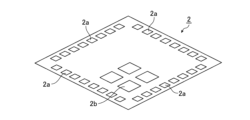
図1は、半導体パッケージ1の構成を示す平面図である。図1(a)は、半導体チップ2を収容する半導体パッケージ1の内部構成を示す平面図であり、内部構成を示すためにパッケージの封止樹脂の記載が省略されている。図1(b)は、半導体チップ2の構成を概略的に示す平面図である。図2は、半導体チップ2を示す斜視図である。半導体パッケージ1は、実施の形態1に係る半導体装置である。半導体チップ2は、パッケージ基板3に配置されている。パッケージ基板3の周縁部には、図1(a)に示すように、外側に延びた複数のリード4が設けられ、半導体チップ2の周縁部には、複数の電極パッド2aが設けられている。電極パッド2aは、ワイヤ5によってリード4と接続されるボンディングパッドである。
Claims (4)
- データを記憶するメモリを有する半導体チップと、
前記メモリに直接接続され、前記半導体チップにおける前記メモリの上部に設けられたデータ読み出し用電極と、
前記半導体チップを収容するパッケージと、
前記パッケージの外表面における前記データ読み出し用電極に対応する位置に設けられた電極指標部と、を備えた
ことを特徴とする半導体装置。 - 前記電極指標部は、前記パッケージの外表面に設けられた凹部である
ことを特徴とする請求項1に記載の半導体装置。 - 前記電極指標部は、前記パッケージの外表面に設けられたマークである
ことを特徴とする請求項1に記載の半導体装置。 - パッケージ基板に積層された複数の前記半導体チップと、
前記半導体チップを積層方向に貫通し、前記半導体チップ間の回路を電気的に接続する貫通電極と、を備え、
前記データ読み出し用電極は、前記パッケージ基板から最も離れて積層された前記半導体チップにおける前記メモリの上部に設けられた
ことを特徴とする請求項1から請求項3のいずれか1項に記載の半導体装置。
Priority Applications (1)
| Application Number | Priority Date | Filing Date | Title |
|---|---|---|---|
| JP2020168162A JP7561563B2 (ja) | 2020-10-05 | 2020-10-05 | 半導体装置 |
Applications Claiming Priority (1)
| Application Number | Priority Date | Filing Date | Title |
|---|---|---|---|
| JP2020168162A JP7561563B2 (ja) | 2020-10-05 | 2020-10-05 | 半導体装置 |
Publications (2)
| Publication Number | Publication Date |
|---|---|
| JP2022060614A JP2022060614A (ja) | 2022-04-15 |
| JP7561563B2 true JP7561563B2 (ja) | 2024-10-04 |
Family
ID=81125377
Family Applications (1)
| Application Number | Title | Priority Date | Filing Date |
|---|---|---|---|
| JP2020168162A Active JP7561563B2 (ja) | 2020-10-05 | 2020-10-05 | 半導体装置 |
Country Status (1)
| Country | Link |
|---|---|
| JP (1) | JP7561563B2 (ja) |
Citations (4)
| Publication number | Priority date | Publication date | Assignee | Title |
|---|---|---|---|---|
| JP2006157047A (ja) | 1995-03-30 | 2006-06-15 | Renesas Technology Corp | 半導体パッケージ |
| JP2010249824A (ja) | 1998-12-31 | 2010-11-04 | Formfactor Inc | 半導体製品ダイのテスト方法及び同テストのためのテストダイを含むアセンブリ |
| JP2011100898A (ja) | 2009-11-06 | 2011-05-19 | Sony Corp | 半導体デバイス |
| JP2013131533A (ja) | 2011-12-20 | 2013-07-04 | Elpida Memory Inc | 半導体装置 |
-
2020
- 2020-10-05 JP JP2020168162A patent/JP7561563B2/ja active Active
Patent Citations (4)
| Publication number | Priority date | Publication date | Assignee | Title |
|---|---|---|---|---|
| JP2006157047A (ja) | 1995-03-30 | 2006-06-15 | Renesas Technology Corp | 半導体パッケージ |
| JP2010249824A (ja) | 1998-12-31 | 2010-11-04 | Formfactor Inc | 半導体製品ダイのテスト方法及び同テストのためのテストダイを含むアセンブリ |
| JP2011100898A (ja) | 2009-11-06 | 2011-05-19 | Sony Corp | 半導体デバイス |
| JP2013131533A (ja) | 2011-12-20 | 2013-07-04 | Elpida Memory Inc | 半導体装置 |
Also Published As
| Publication number | Publication date |
|---|---|
| JP2022060614A (ja) | 2022-04-15 |
Similar Documents
| Publication | Publication Date | Title |
|---|---|---|
| US6028774A (en) | Base cards and IC cards using the same | |
| US6670221B2 (en) | Semiconductor device having a built-in contact-type sensor and manufacturing method thereof | |
| US7812356B2 (en) | Method of assembling semiconductor devices with LEDS | |
| JP2007194436A (ja) | 半導体パッケージ、導電性ポスト付き基板、積層型半導体装置、半導体パッケージの製造方法及び積層型半導体装置の製造方法 | |
| KR100266071B1 (ko) | 칩 온 보드 패키지용 인쇄회로기판 및 그를 이용한 칩 온 보드 패키지 | |
| US10395087B2 (en) | Biometric sensing chip and electronic device using same | |
| JPH04212445A (ja) | Icパッケージ | |
| KR20010002214A (ko) | 반도체패키지와 그 제조방법 | |
| TWI520137B (zh) | 半導體記憶裝置及其製造方法 | |
| JP7561563B2 (ja) | 半導体装置 | |
| JP5597659B2 (ja) | 半導体メモリカード | |
| JP2006203211A (ja) | マルチチップモジュールに架橋層を使用する信号再配信 | |
| KR100995961B1 (ko) | 플래시 메모리 카드 제조방법 | |
| CN111384053B (zh) | 微控制器及其制作方法 | |
| US20080156884A1 (en) | Memory card having double contact pads and method for manufacturing the same | |
| US11252817B1 (en) | Printed wiring board and memory system | |
| JP2000172821A5 (ja) | ||
| JP4583850B2 (ja) | 半導体装置及びその製造方法 | |
| JP2006351664A (ja) | 半導体装置 | |
| US7126836B2 (en) | Semiconductor device, system device using it, and manufacturing method of a semiconductor device | |
| US20240324112A1 (en) | Semiconductor storage device | |
| JP2000123141A (ja) | メモリカード | |
| CN218274562U (zh) | 一种可靠性高的台面结构芯片 | |
| US20070210175A1 (en) | Semiconductor memory card | |
| KR20000061036A (ko) | 칩 카드용 베이스 기판 및 그를 이용한 칩 카드 |
Legal Events
| Date | Code | Title | Description |
|---|---|---|---|
| A621 | Written request for application examination |
Free format text: JAPANESE INTERMEDIATE CODE: A621 Effective date: 20230703 |
|
| A977 | Report on retrieval |
Free format text: JAPANESE INTERMEDIATE CODE: A971007 Effective date: 20240515 |
|
| A131 | Notification of reasons for refusal |
Free format text: JAPANESE INTERMEDIATE CODE: A131 Effective date: 20240618 |
|
| A521 | Request for written amendment filed |
Free format text: JAPANESE INTERMEDIATE CODE: A523 Effective date: 20240802 |
|
| TRDD | Decision of grant or rejection written | ||
| A01 | Written decision to grant a patent or to grant a registration (utility model) |
Free format text: JAPANESE INTERMEDIATE CODE: A01 Effective date: 20240827 |
|
| A61 | First payment of annual fees (during grant procedure) |
Free format text: JAPANESE INTERMEDIATE CODE: A61 Effective date: 20240924 |
|
| R150 | Certificate of patent or registration of utility model |
Ref document number: 7561563 Country of ref document: JP Free format text: JAPANESE INTERMEDIATE CODE: R150 |