JP7561563B2 - Semiconductor Device - Google Patents
Semiconductor Device Download PDFInfo
- Publication number
- JP7561563B2 JP7561563B2 JP2020168162A JP2020168162A JP7561563B2 JP 7561563 B2 JP7561563 B2 JP 7561563B2 JP 2020168162 A JP2020168162 A JP 2020168162A JP 2020168162 A JP2020168162 A JP 2020168162A JP 7561563 B2 JP7561563 B2 JP 7561563B2
- Authority
- JP
- Japan
- Prior art keywords
- memory
- semiconductor
- package
- electrode
- data
- Prior art date
- Legal status (The legal status is an assumption and is not a legal conclusion. Google has not performed a legal analysis and makes no representation as to the accuracy of the status listed.)
- Active
Links
- 239000004065 semiconductor Substances 0.000 title claims description 99
- 230000015654 memory Effects 0.000 claims description 52
- 239000000758 substrate Substances 0.000 claims description 10
- 238000007789 sealing Methods 0.000 description 7
- 230000002159 abnormal effect Effects 0.000 description 5
- 239000011347 resin Substances 0.000 description 5
- 229920005989 resin Polymers 0.000 description 5
- 238000004891 communication Methods 0.000 description 4
- 230000007257 malfunction Effects 0.000 description 4
- 239000000523 sample Substances 0.000 description 3
- 239000000853 adhesive Substances 0.000 description 2
- 230000001070 adhesive effect Effects 0.000 description 2
- 238000000034 method Methods 0.000 description 2
- 230000002093 peripheral effect Effects 0.000 description 2
- 239000002904 solvent Substances 0.000 description 2
- 230000007547 defect Effects 0.000 description 1
- 238000005553 drilling Methods 0.000 description 1
- 230000006870 function Effects 0.000 description 1
- 230000001678 irradiating effect Effects 0.000 description 1
- 239000000463 material Substances 0.000 description 1
- 230000007704 transition Effects 0.000 description 1
- XLYOFNOQVPJJNP-UHFFFAOYSA-N water Substances O XLYOFNOQVPJJNP-UHFFFAOYSA-N 0.000 description 1
Images


Landscapes
- Semiconductor Integrated Circuits (AREA)
- Metal-Oxide And Bipolar Metal-Oxide Semiconductor Integrated Circuits (AREA)
- Semiconductor Memories (AREA)
- Non-Volatile Memory (AREA)
- Structures Or Materials For Encapsulating Or Coating Semiconductor Devices Or Solid State Devices (AREA)
- Internal Circuitry In Semiconductor Integrated Circuit Devices (AREA)
Description
本開示は、不揮発性メモリを有した半導体装置に関する。 This disclosure relates to a semiconductor device having a non-volatile memory.
1チップ化または1パッケージ化された半導体装置は、様々な電子機器に利用されている。例えば、ドライブレコーダ、監視カメラまたはスマートフォンといった電子機器は、大容量のデータが取り扱われ、さらにデータに高度なセキュリティが必要とされる。このため、半導体装置に不具合が発生した際に、チップまたはパッケージの内部のメモリからデータを安全に読み出し可能であることが要求される。 Single-chip or single-packaged semiconductor devices are used in a variety of electronic devices. For example, electronic devices such as drive recorders, surveillance cameras, and smartphones handle large volumes of data, and a high level of security is required for that data. For this reason, when a malfunction occurs in the semiconductor device, it is required that data can be safely read from the memory inside the chip or package.
例えば、特許文献1に記載された半導体装置は、モジュール出力端子が非通常状態であるか否かをMON端子から検出し、モジュール出力端子が非通常状態であるときに通常モードからデータ通信モードに移行して、モジュール出力端子ないしはモジュール電源端子を流用してセンサモジュール外部とのデータ通信を行う。これにより、特許文献1に記載された半導体装置は、非通常状態になっても、モジュール出力端子またはモジュール電源端子といった外部端子からデータを取り出すことができる。外部端子は、電極パッドまたはリードフレームである。 For example, the semiconductor device described in Patent Document 1 detects from the MON terminal whether the module output terminal is in an abnormal state, and when the module output terminal is in an abnormal state, transitions from normal mode to data communication mode and uses the module output terminal or the module power supply terminal to perform data communication with the outside of the sensor module. As a result, even when the semiconductor device described in Patent Document 1 is in an abnormal state, it can extract data from external terminals such as the module output terminal or the module power supply terminal. The external terminals are electrode pads or lead frames.
しかしながら、電子機器において、電源トラブルによって半導体装置の外部端子に意図しない高電圧が印加されると、外部端子が破壊されて非導通状態になる場合がある。この場合、特許文献1に記載された半導体装置は、内部のメモリからデータを読み出せなくなるという課題があった。 However, in electronic devices, if a power supply problem causes an unintended high voltage to be applied to the external terminals of a semiconductor device, the external terminals may be destroyed and become non-conductive. In this case, the semiconductor device described in Patent Document 1 has the problem that data cannot be read from its internal memory.
本開示は上記課題を解決するものであり、外部端子が非道通状態になってもメモリからデータを読み出すことができる半導体装置を得ることを目的とする。 The present disclosure aims to solve the above problem and provide a semiconductor device that can read data from memory even if the external terminal is in a non-conductive state.
本開示に係る半導体装置は、データを記憶するメモリを有する半導体チップと、メモリに直接接続され、半導体チップにおけるメモリの上部に設けられたデータ読み出し用電極と、半導体チップを収容するパッケージと、パッケージの外表面におけるデータ読み出し用電極に対応する位置に設けられた電極指標部と、を備える。 The semiconductor device according to the present disclosure comprises a semiconductor chip having a memory for storing data, a data reading electrode directly connected to the memory and provided on top of the memory in the semiconductor chip , a package for accommodating the semiconductor chip, and an electrode indicator portion provided at a position corresponding to the data reading electrode on the outer surface of the package .
本開示によれば、メモリに直接接続され、半導体チップにおけるメモリの上部に設けられたデータ読み出し用電極を備えるので、本開示に係る半導体装置は、外部端子が非道通状態になってもメモリからデータを読み出すことができる。 According to the present disclosure, the semiconductor device according to the present disclosure is provided with a data read electrode that is directly connected to the memory and is provided above the memory in the semiconductor chip, so that the semiconductor device according to the present disclosure can read data from the memory even if the external terminal becomes non-conductive.
実施の形態1.
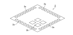
図1は、半導体パッケージ1の構成を示す平面図である。図1(a)は、半導体チップ2を収容する半導体パッケージ1の内部構成を示す平面図であり、内部構成を示すためにパッケージの封止樹脂の記載が省略されている。図1(b)は、半導体チップ2の構成を概略的に示す平面図である。図2は、半導体チップ2を示す斜視図である。半導体パッケージ1は、実施の形態1に係る半導体装置である。半導体チップ2は、パッケージ基板3に配置されている。パッケージ基板3の周縁部には、図1(a)に示すように、外側に延びた複数のリード4が設けられ、半導体チップ2の周縁部には、複数の電極パッド2aが設けられている。電極パッド2aは、ワイヤ5によってリード4と接続されるボンディングパッドである。
Embodiment 1.
FIG. 1 is a plan view showing the configuration of a semiconductor package 1. FIG. 1(a) is a plan view showing the internal configuration of a semiconductor package 1 that accommodates a
半導体チップ2は、図1(b)に示すように、メモリ2c、ロジック回路2d、アナログ回路2eおよびインタフェース回路2fが1つのチップに集積された大規模集積回路、いわゆるSoC(System on a Chip)である。メモリ2cは、半導体チップ2が取り扱うデータを記憶する不揮発性メモリであり、例えば、NANDフラッシュメモリである。ロジック回路2dは、デジタル信号を処理し、アナログ回路2eは、アナログ信号を処理する。インタフェース回路2fは、電極パッド2aを介した信号の送受信に加え、インタフェース回路2f、ロジック回路2dおよびアナログ回路2eへの電源の供給を実行する。
As shown in FIG. 1(b), the
メモリ2cの動作電源は、半導体チップ2の内部で生成され、インタフェース回路2f、ロジック回路2dおよびアナログ回路2eの動作電源とは異なる。このため、メモリ2cは、周辺回路から切り離して動作させることが可能である。
The operating power supply for memory 2c is generated inside
半導体パッケージ1において、ワイヤ5によって電極パッド2aとリード4とが接続されたものが、外部端子である。外部端子には、電極パッド2aがインタフェース回路2fによってメモリ2cと接続されたものも含まれる。半導体チップ2には、パッケージ基板3と対向する第1の面と、その反対側の第2の面がある。図1(a)は、半導体チップ2を第2の面側から見たものである。半導体チップ2には、図2に示すように、電極パッド2aとは別に、電極パッド2bが設けられている。電極パッド2bは、インタフェース回路2fを介さずにメモリ2cに直接接続され、半導体チップ2におけるメモリ2cの上部に設けられたデータ読み出し用電極である。
In the semiconductor package 1, the
メモリ2cは、周辺回路から切り離して動作させることができるので、電極パッド2bを介してメモリ2cを直接動作させてデータを読み出すことが可能である。例えば、図1(a)において、破線の矢印Aで示すように、電源トラブルによって耐圧を超える高電圧が外部端子に印加されることで外部端子が破壊されたものとする。図1(a)において、太線の矢印BにX印を付して示すように、メモリ2cに記憶されたデータを、リード4を介して読み出すことができなくなる。
Memory 2c can be operated separately from the peripheral circuits, so it is possible to directly operate memory 2c via
これに対し、半導体チップ2は、図1(a)において太線の矢印Cで示すように、電極パッド2bを介してメモリ2cを直接動作させることで、メモリ2cからデータを読み出すことが可能である。従来の半導体装置においても、非通常状態になった場合に、半導体チップ2の内部に設けられたメモリからデータを読み出す、いわゆるデータの救済を行うものはあった。例えば、データを外部に引き出す外部端子の一つとして、データ読み出し専用の端子を設けた半導体装置がある。また、メモリに記憶されたデータを無線で外部に送信する通信回路を設けた半導体装置がある。
In contrast, the
しかしながら、データを外部に引き出す外部端子の一つとして、データ読み出し専用の端子を設けた場合、外部端子を介して接続された外部装置との間で発生した電源トラブルなどの不具合によって外部端子が破壊されることがある。この場合、データ読み出し専用の端子を介したデータ読み出しができなくなる。また、半導体装置にデータ読み出し専用端子を新たに追加する場合、外部端子の数が増加されるので、半導体装置の小型化が制限される。同様に、通信回路を設けた半導体装置においても、回路の追加に伴う面積増加によって小型化が制限される。 However, if a terminal dedicated to reading data is provided as one of the external terminals for extracting data to the outside, the external terminal may be destroyed by a malfunction such as a power supply problem that occurs between the external device connected via the external terminal. In this case, data cannot be read via the terminal dedicated to reading data. Furthermore, when a new terminal dedicated to reading data is added to a semiconductor device, the number of external terminals increases, limiting miniaturization of the semiconductor device. Similarly, miniaturization of a semiconductor device provided with a communication circuit is also limited by the increase in area that accompanies the addition of the circuit.
半導体パッケージ1は、メモリ2cに直接接続されて、半導体チップ2におけるメモリ2cの上部に設けられた電極パッド2bを備える。電極パッド2bは、通常、外部装置と接続される外部端子ではなく、外部装置との間で発生した不具合の影響を受けない。また、電極パッド2bは、メモリ2cの上部に設けられるので、電極の追加に伴う面積の増加がなく、半導体パッケージ1の小型化が可能である。
The semiconductor package 1 is directly connected to the memory 2c and has
図3は、半導体パッケージ1を示す斜視図である。半導体パッケージ1は、封止樹脂によって半導体チップ2がモールドされた、いわゆるSiP(System in Package)である。半導体パッケージ1において、外表面における電極パッド2bに対応する位置には、図3に示すように、凹部6が設けられる。凹部6は、半導体パッケージ1の外側から電極パッド2bの位置を示す電極指標部である。
Figure 3 is a perspective view showing a semiconductor package 1. The semiconductor package 1 is a so-called SiP (System in Package) in which a
図4は、半導体パッケージ1の構造を示す断面図である。図4(a)は、通常状態の半導体パッケージ1を示す断面図であり、図4(b)は、電極パッド2bを介して、メモリ2cからデータを読み出す際の半導体パッケージ1を示す断面図である。通常状態の半導体パッケージ1において、メモリ2cに記憶されたデータは、外部端子を介して読み出され、電極パッド2bは使用されない。このため、凹部6は、半導体パッケージ1の内部に水などが侵入しないように、図4(a)に示すように、電極パッド2bは露出しない程度の深さで形成されている。
Figure 4 is a cross-sectional view showing the structure of the semiconductor package 1. Figure 4(a) is a cross-sectional view showing the semiconductor package 1 in a normal state, and Figure 4(b) is a cross-sectional view showing the semiconductor package 1 when data is read from the memory 2c via the
半導体パッケージ1が非通常状態になり、メモリ2cからデータを救済する必要がある場合、凹部6は、電極パッド2bが露出するまで凹部6の底面が穿たれる。凹部6の底面を穿つ方法には、例えば、ドリルを用いて底面に穴を開ける方法があり、または、溶剤を用いて底面を溶かして電極パッド2bをパッケージ外部に露出させる方法がある。データの読み取り装置100が備えるプローブ針101は、図4(b)に示すように、凹部6を通して電極パッド2bと接触され、電極パッド2bを介して、メモリ2cに記憶されたデータが読み出される。
When the semiconductor package 1 is in an abnormal state and data needs to be rescued from the memory 2c, the bottom of the
図5は、半導体パッケージ1の変形例1である、半導体パッケージ1Aを示す平面図である。半導体パッケージ1Aにおいて、外表面における電極パッド2bに対応する位置には、図5に示すように、マーク6Aが設けられる。マーク6Aは、半導体パッケージ1Aの外側から電極パッド2bの位置を示す電極指標部であり、例えば、シルク印刷によって半導体パッケージ1Aの外表面に形成されている。マーク6Aが施された部分に穴を開けるか、または、溶剤を用いてマーク6Aが施された部分の一部を溶かすことにより、電極パッド2bは、パッケージ外部に露出する。外部に露出された電極パッド2bは、プローブ針101に接触され、読み取り装置100は、電極パッド2bを介してメモリ2cに記憶されたデータを読み出す。
Figure 5 is a plan view showing a
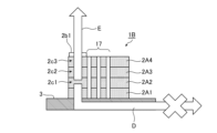
図6は、半導体パッケージ1の変形例2である半導体パッケージ1Bの構成を示す部分断面図であり、内部構成を示すために、パッケージの封止樹脂の記載が省略されている。半導体パッケージ1Bは、図6に示すように、パッケージ基板3上に、半導体チップ2A1、2A2、2A3および2A4が積層された構成を有している。半導体チップ2A1、2A2、2A3および2A4において、半導体チップ間の回路は、ビアホール17により電気的に接続される。ビアホール17は、半導体チップの積層方向に貫通した貫通電極である。
Figure 6 is a partial cross-sectional view showing the configuration of
パッケージ基板3上に積層された半導体チップ2A1には、半導体チップ2A2、2A3および2A4が備える回路を制御するコントローラとして機能するロジック回路が設けられている。また、半導体チップ2A2、2A3および2A4には、メモリ2c1、2c2および2c3が設けられている。メモリ2c1、2c2および2c3にデータを記憶することができるので、半導体パッケージ1Bは、大容量のデータを保存することが可能である。
The semiconductor chip 2A1 stacked on the
半導体パッケージ1Bは、半導体チップ2A1に設けられた電極パッド2aと、パッケージ基板3に設けられたリード4とが、ワイヤ5によって接続された外部端子を備える。半導体チップ2A4は、外部端子とは別に、電極パッド2b1を備えている。電極パッド2b1は、メモリ2c3に直接接続されており、パッケージ基板3から最も離れた半導体チップ2A4におけるメモリ2c3の上部に設けられたデータ読み出し用電極である。
The
メモリ2c1、2c2および2c3は、ビアホール17によって接続されており、半導体パッケージ1Bが通常状態である場合、メモリ2c1、2c2および2c3に記憶されたデータは、矢印Dに示すように、外部端子を介して外部装置に読み出される。外部装置との不具合によって外部端子が破壊された場合、矢印DにX印を付して示すように、外部端子を介したデータ読み出しができなくなる。これに対し、半導体パッケージ1Bでは、矢印Eに示すように、電極パッド2b1を介して、メモリ2c1、2c2および2c3に記憶されたデータが読み出すことが可能である。
Memories 2c1, 2c2, and 2c3 are connected by via
なお、図3には電極指標部が凹部6である場合を示したが、電極指標部は、メモリ2cの位置を示す凸部であってもよい。また、図5において、マーク6Aが矩形のマークである場合を示したが、電極指標部は、矩形以外の形状のマークであってもよい。電極指標部は、その下部に電極パッド2bがあることが外側から認識可能であればよく、例えば、円形であってもよいし、X印であってもよい。
In addition, while FIG. 3 shows a case where the electrode indicator portion is a
また、図3の説明において、凹部6の底面を穿って電極パッド2bを外部に露出させる場合を示したが、凹部6は、電極パッド2bが露出するまで封止樹脂が貫通された孔部であってもよい。この場合、凹部6の開口部は、シール部材によって塞がれる。シール部材は、通常、凹部6の開口部を覆うように強固に接着するが、一定の処理を施すことにより凹部6の開口部から容易に剥がれる部材が好ましい。例えば、接着剤に紫外線硬化樹脂を含むシール部材は、紫外線を照射することにより接着剤が硬化収縮して容易に剥がすことができる。
In addition, in the explanation of FIG. 3, the bottom surface of the
以上のように、実施の形態1に係る半導体パッケージ1は、データを記憶するメモリ2cを有する半導体チップ2と、メモリ2cに直接接続され、半導体チップ2におけるメモリ2cの上部に設けられた電極パッド2bとを備える。電極パッド2bは、通常、外部装置と接続される外部端子ではなく、外部装置との間で発生した不具合の影響を受けない。このため、外部端子が非道通状態になってもメモリ2cからデータを読み出すことができる。さらに、電極パッド2bは、メモリ2cの上部に設けられるので、電極の追加に伴う面積の増加がなく、半導体パッケージ1の小型化が可能である。
As described above, the semiconductor package 1 according to the first embodiment includes a
なお、実施の形態の任意の構成要素の変形もしくは実施の形態の任意の構成要素の省略が可能である。 In addition, any of the components of the embodiments may be modified or omitted.
1,1A,1B 半導体パッケージ、2,2A1,2A2,2A3,2A4 半導体チップ、2a,2b,2b1 電極パッド、2c,2c1,2c2,2c3 メモリ、2d ロジック回路、2e アナログ回路、2f インタフェース回路、3 パッケージ基板、4 リード、5 ワイヤ、6 凹部、6A マーク、17 ビアホール、100 読み取り装置、101 プローブ針。 1, 1A, 1B semiconductor package, 2, 2A1, 2A2, 2A3, 2A4 semiconductor chip, 2a, 2b, 2b1 electrode pad, 2c, 2c1, 2c2, 2c3 memory, 2d logic circuit, 2e analog circuit, 2f interface circuit, 3 package substrate, 4 lead, 5 wire, 6 recess, 6A mark, 17 via hole, 100 reading device, 101 probe needle.
Claims (4)
前記メモリに直接接続され、前記半導体チップにおける前記メモリの上部に設けられたデータ読み出し用電極と、
前記半導体チップを収容するパッケージと、
前記パッケージの外表面における前記データ読み出し用電極に対応する位置に設けられた電極指標部と、を備えた
ことを特徴とする半導体装置。 A semiconductor chip having a memory for storing data;
a data read electrode directly connected to the memory and provided on an upper portion of the memory in the semiconductor chip;
a package that houses the semiconductor chip;
an electrode indicator portion provided on an outer surface of the package at a position corresponding to the data read electrode .
ことを特徴とする請求項1に記載の半導体装置。 2. The semiconductor device according to claim 1 , wherein the electrode indicator portion is a recess provided on an outer surface of the package.
ことを特徴とする請求項1に記載の半導体装置。 2. The semiconductor device according to claim 1 , wherein the electrode indicator portion is a mark provided on an outer surface of the package.
前記半導体チップを積層方向に貫通し、前記半導体チップ間の回路を電気的に接続する貫通電極と、を備え、
前記データ読み出し用電極は、前記パッケージ基板から最も離れて積層された前記半導体チップにおける前記メモリの上部に設けられた
ことを特徴とする請求項1から請求項3のいずれか1項に記載の半導体装置。 A plurality of the semiconductor chips stacked on a package substrate;
a through electrode that penetrates the semiconductor chip in a stacking direction and electrically connects circuits between the semiconductor chips;
4. The semiconductor device according to claim 1 , wherein the data read electrode is provided above the memory in the semiconductor chip that is stacked farthest from the package substrate.
Priority Applications (1)
| Application Number | Priority Date | Filing Date | Title |
|---|---|---|---|
| JP2020168162A JP7561563B2 (en) | 2020-10-05 | 2020-10-05 | Semiconductor Device |
Applications Claiming Priority (1)
| Application Number | Priority Date | Filing Date | Title |
|---|---|---|---|
| JP2020168162A JP7561563B2 (en) | 2020-10-05 | 2020-10-05 | Semiconductor Device |
Publications (2)
| Publication Number | Publication Date |
|---|---|
| JP2022060614A JP2022060614A (en) | 2022-04-15 |
| JP7561563B2 true JP7561563B2 (en) | 2024-10-04 |
Family
ID=81125377
Family Applications (1)
| Application Number | Title | Priority Date | Filing Date |
|---|---|---|---|
| JP2020168162A Active JP7561563B2 (en) | 2020-10-05 | 2020-10-05 | Semiconductor Device |
Country Status (1)
| Country | Link |
|---|---|
| JP (1) | JP7561563B2 (en) |
Citations (4)
| Publication number | Priority date | Publication date | Assignee | Title |
|---|---|---|---|---|
| JP2006157047A (en) | 1995-03-30 | 2006-06-15 | Renesas Technology Corp | Semiconductor package |
| JP2010249824A (en) | 1998-12-31 | 2010-11-04 | Formfactor Inc | Semiconductor product die test method and assembly including test die for the test |
| JP2011100898A (en) | 2009-11-06 | 2011-05-19 | Sony Corp | Semiconductor device |
| JP2013131533A (en) | 2011-12-20 | 2013-07-04 | Elpida Memory Inc | Semiconductor device |
-
2020
- 2020-10-05 JP JP2020168162A patent/JP7561563B2/en active Active
Patent Citations (4)
| Publication number | Priority date | Publication date | Assignee | Title |
|---|---|---|---|---|
| JP2006157047A (en) | 1995-03-30 | 2006-06-15 | Renesas Technology Corp | Semiconductor package |
| JP2010249824A (en) | 1998-12-31 | 2010-11-04 | Formfactor Inc | Semiconductor product die test method and assembly including test die for the test |
| JP2011100898A (en) | 2009-11-06 | 2011-05-19 | Sony Corp | Semiconductor device |
| JP2013131533A (en) | 2011-12-20 | 2013-07-04 | Elpida Memory Inc | Semiconductor device |
Also Published As
| Publication number | Publication date |
|---|---|
| JP2022060614A (en) | 2022-04-15 |
Similar Documents
| Publication | Publication Date | Title |
|---|---|---|
| US6028774A (en) | Base cards and IC cards using the same | |
| US6670221B2 (en) | Semiconductor device having a built-in contact-type sensor and manufacturing method thereof | |
| US7812356B2 (en) | Method of assembling semiconductor devices with LEDS | |
| JP2007194436A (en) | Semiconductor package, substrate with conductive post, stacked semiconductor device, manufacturing method of semiconductor package, and manufacturing method of stacked semiconductor device | |
| KR100266071B1 (en) | Printed circuit board for chip on board package and chip on board package | |
| US10395087B2 (en) | Biometric sensing chip and electronic device using same | |
| JPH04212445A (en) | Ic package | |
| KR20010002214A (en) | A semiconductor packages and manufacturing method for it | |
| TWI520137B (en) | Semiconductor memory device and method of manufacturing same | |
| JP7561563B2 (en) | Semiconductor Device | |
| JP5597659B2 (en) | Semiconductor memory card | |
| JP2006203211A (en) | Signal redistribution using cross-linked layers in multichip modules | |
| CN111384053B (en) | Microcontroller and manufacturing method thereof | |
| KR20080088585A (en) | Flash memory card manufacturing method | |
| US20080156884A1 (en) | Memory card having double contact pads and method for manufacturing the same | |
| US11252817B1 (en) | Printed wiring board and memory system | |
| JP2000172821A5 (en) | ||
| JP4583850B2 (en) | Semiconductor device and manufacturing method thereof | |
| JP2006351664A (en) | Semiconductor device | |
| US7126836B2 (en) | Semiconductor device, system device using it, and manufacturing method of a semiconductor device | |
| US20240324112A1 (en) | Semiconductor storage device | |
| JP2000123141A (en) | Memory card | |
| CN218274562U (en) | Mesa structure chip that reliability is high | |
| KR100919218B1 (en) | Cob-type chip package built-in led for a memory card, and manufacturing method thereof | |
| US20070210175A1 (en) | Semiconductor memory card |
Legal Events
| Date | Code | Title | Description |
|---|---|---|---|
| A621 | Written request for application examination |
Free format text: JAPANESE INTERMEDIATE CODE: A621 Effective date: 20230703 |
|
| A977 | Report on retrieval |
Free format text: JAPANESE INTERMEDIATE CODE: A971007 Effective date: 20240515 |
|
| A131 | Notification of reasons for refusal |
Free format text: JAPANESE INTERMEDIATE CODE: A131 Effective date: 20240618 |
|
| A521 | Request for written amendment filed |
Free format text: JAPANESE INTERMEDIATE CODE: A523 Effective date: 20240802 |
|
| TRDD | Decision of grant or rejection written | ||
| A01 | Written decision to grant a patent or to grant a registration (utility model) |
Free format text: JAPANESE INTERMEDIATE CODE: A01 Effective date: 20240827 |
|
| A61 | First payment of annual fees (during grant procedure) |
Free format text: JAPANESE INTERMEDIATE CODE: A61 Effective date: 20240924 |
|
| R150 | Certificate of patent or registration of utility model |
Ref document number: 7561563 Country of ref document: JP Free format text: JAPANESE INTERMEDIATE CODE: R150 |