JP7561518B2 - 表示装置 - Google Patents
表示装置 Download PDFInfo
- Publication number
- JP7561518B2 JP7561518B2 JP2020086041A JP2020086041A JP7561518B2 JP 7561518 B2 JP7561518 B2 JP 7561518B2 JP 2020086041 A JP2020086041 A JP 2020086041A JP 2020086041 A JP2020086041 A JP 2020086041A JP 7561518 B2 JP7561518 B2 JP 7561518B2
- Authority
- JP
- Japan
- Prior art keywords
- light
- emitting element
- electrode
- led chip
- voltage
- Prior art date
- Legal status (The legal status is an assumption and is not a legal conclusion. Google has not performed a legal analysis and makes no representation as to the accuracy of the status listed.)
- Active
Links
Images


Classifications
-
- G—PHYSICS
- G09—EDUCATION; CRYPTOGRAPHY; DISPLAY; ADVERTISING; SEALS
- G09G—ARRANGEMENTS OR CIRCUITS FOR CONTROL OF INDICATING DEVICES USING STATIC MEANS TO PRESENT VARIABLE INFORMATION
- G09G3/00—Control arrangements or circuits, of interest only in connection with visual indicators other than cathode-ray tubes
- G09G3/20—Control arrangements or circuits, of interest only in connection with visual indicators other than cathode-ray tubes for presentation of an assembly of a number of characters, e.g. a page, by composing the assembly by combination of individual elements arranged in a matrix no fixed position being assigned to or needed to be assigned to the individual characters or partial characters
- G09G3/22—Control arrangements or circuits, of interest only in connection with visual indicators other than cathode-ray tubes for presentation of an assembly of a number of characters, e.g. a page, by composing the assembly by combination of individual elements arranged in a matrix no fixed position being assigned to or needed to be assigned to the individual characters or partial characters using controlled light sources
- G09G3/30—Control arrangements or circuits, of interest only in connection with visual indicators other than cathode-ray tubes for presentation of an assembly of a number of characters, e.g. a page, by composing the assembly by combination of individual elements arranged in a matrix no fixed position being assigned to or needed to be assigned to the individual characters or partial characters using controlled light sources using electroluminescent panels
- G09G3/32—Control arrangements or circuits, of interest only in connection with visual indicators other than cathode-ray tubes for presentation of an assembly of a number of characters, e.g. a page, by composing the assembly by combination of individual elements arranged in a matrix no fixed position being assigned to or needed to be assigned to the individual characters or partial characters using controlled light sources using electroluminescent panels semiconductive, e.g. using light-emitting diodes [LED]
-
- G—PHYSICS
- G09—EDUCATION; CRYPTOGRAPHY; DISPLAY; ADVERTISING; SEALS
- G09G—ARRANGEMENTS OR CIRCUITS FOR CONTROL OF INDICATING DEVICES USING STATIC MEANS TO PRESENT VARIABLE INFORMATION
- G09G3/00—Control arrangements or circuits, of interest only in connection with visual indicators other than cathode-ray tubes
- G09G3/20—Control arrangements or circuits, of interest only in connection with visual indicators other than cathode-ray tubes for presentation of an assembly of a number of characters, e.g. a page, by composing the assembly by combination of individual elements arranged in a matrix no fixed position being assigned to or needed to be assigned to the individual characters or partial characters
- G09G3/2007—Display of intermediate tones
- G09G3/2018—Display of intermediate tones by time modulation using two or more time intervals
- G09G3/2022—Display of intermediate tones by time modulation using two or more time intervals using sub-frames
-
- G—PHYSICS
- G09—EDUCATION; CRYPTOGRAPHY; DISPLAY; ADVERTISING; SEALS
- G09G—ARRANGEMENTS OR CIRCUITS FOR CONTROL OF INDICATING DEVICES USING STATIC MEANS TO PRESENT VARIABLE INFORMATION
- G09G3/00—Control arrangements or circuits, of interest only in connection with visual indicators other than cathode-ray tubes
- G09G3/20—Control arrangements or circuits, of interest only in connection with visual indicators other than cathode-ray tubes for presentation of an assembly of a number of characters, e.g. a page, by composing the assembly by combination of individual elements arranged in a matrix no fixed position being assigned to or needed to be assigned to the individual characters or partial characters
- G09G3/2007—Display of intermediate tones
- G09G3/207—Display of intermediate tones by domain size control
-
- G—PHYSICS
- G09—EDUCATION; CRYPTOGRAPHY; DISPLAY; ADVERTISING; SEALS
- G09G—ARRANGEMENTS OR CIRCUITS FOR CONTROL OF INDICATING DEVICES USING STATIC MEANS TO PRESENT VARIABLE INFORMATION
- G09G3/00—Control arrangements or circuits, of interest only in connection with visual indicators other than cathode-ray tubes
- G09G3/20—Control arrangements or circuits, of interest only in connection with visual indicators other than cathode-ray tubes for presentation of an assembly of a number of characters, e.g. a page, by composing the assembly by combination of individual elements arranged in a matrix no fixed position being assigned to or needed to be assigned to the individual characters or partial characters
- G09G3/2007—Display of intermediate tones
- G09G3/2077—Display of intermediate tones by a combination of two or more gradation control methods
- G09G3/2081—Display of intermediate tones by a combination of two or more gradation control methods with combination of amplitude modulation and time modulation
-
- H—ELECTRICITY
- H01—ELECTRIC ELEMENTS
- H01L—SEMICONDUCTOR DEVICES NOT COVERED BY CLASS H10
- H01L25/00—Assemblies consisting of a plurality of semiconductor or other solid state devices
- H01L25/16—Assemblies consisting of a plurality of semiconductor or other solid state devices the devices being of types provided for in two or more different subclasses of H10B, H10D, H10F, H10H, H10K or H10N, e.g. forming hybrid circuits
- H01L25/167—Assemblies consisting of a plurality of semiconductor or other solid state devices the devices being of types provided for in two or more different subclasses of H10B, H10D, H10F, H10H, H10K or H10N, e.g. forming hybrid circuits comprising optoelectronic devices, e.g. LED, photodiodes
-
- G—PHYSICS
- G09—EDUCATION; CRYPTOGRAPHY; DISPLAY; ADVERTISING; SEALS
- G09G—ARRANGEMENTS OR CIRCUITS FOR CONTROL OF INDICATING DEVICES USING STATIC MEANS TO PRESENT VARIABLE INFORMATION
- G09G2300/00—Aspects of the constitution of display devices
- G09G2300/04—Structural and physical details of display devices
- G09G2300/0421—Structural details of the set of electrodes
- G09G2300/0426—Layout of electrodes and connections
-
- G—PHYSICS
- G09—EDUCATION; CRYPTOGRAPHY; DISPLAY; ADVERTISING; SEALS
- G09G—ARRANGEMENTS OR CIRCUITS FOR CONTROL OF INDICATING DEVICES USING STATIC MEANS TO PRESENT VARIABLE INFORMATION
- G09G2300/00—Aspects of the constitution of display devices
- G09G2300/04—Structural and physical details of display devices
- G09G2300/0439—Pixel structures
- G09G2300/0452—Details of colour pixel setup, e.g. pixel composed of a red, a blue and two green components
-
- G—PHYSICS
- G09—EDUCATION; CRYPTOGRAPHY; DISPLAY; ADVERTISING; SEALS
- G09G—ARRANGEMENTS OR CIRCUITS FOR CONTROL OF INDICATING DEVICES USING STATIC MEANS TO PRESENT VARIABLE INFORMATION
- G09G2300/00—Aspects of the constitution of display devices
- G09G2300/08—Active matrix structure, i.e. with use of active elements, inclusive of non-linear two terminal elements, in the pixels together with light emitting or modulating elements
- G09G2300/0809—Several active elements per pixel in active matrix panels
- G09G2300/0819—Several active elements per pixel in active matrix panels used for counteracting undesired variations, e.g. feedback or autozeroing
-
- G—PHYSICS
- G09—EDUCATION; CRYPTOGRAPHY; DISPLAY; ADVERTISING; SEALS
- G09G—ARRANGEMENTS OR CIRCUITS FOR CONTROL OF INDICATING DEVICES USING STATIC MEANS TO PRESENT VARIABLE INFORMATION
- G09G2300/00—Aspects of the constitution of display devices
- G09G2300/08—Active matrix structure, i.e. with use of active elements, inclusive of non-linear two terminal elements, in the pixels together with light emitting or modulating elements
- G09G2300/0809—Several active elements per pixel in active matrix panels
- G09G2300/0842—Several active elements per pixel in active matrix panels forming a memory circuit, e.g. a dynamic memory with one capacitor
- G09G2300/0861—Several active elements per pixel in active matrix panels forming a memory circuit, e.g. a dynamic memory with one capacitor with additional control of the display period without amending the charge stored in a pixel memory, e.g. by means of additional select electrodes
-
- G—PHYSICS
- G09—EDUCATION; CRYPTOGRAPHY; DISPLAY; ADVERTISING; SEALS
- G09G—ARRANGEMENTS OR CIRCUITS FOR CONTROL OF INDICATING DEVICES USING STATIC MEANS TO PRESENT VARIABLE INFORMATION
- G09G2310/00—Command of the display device
- G09G2310/02—Addressing, scanning or driving the display screen or processing steps related thereto
- G09G2310/0264—Details of driving circuits
- G09G2310/0267—Details of drivers for scan electrodes, other than drivers for liquid crystal, plasma or OLED displays
-
- G—PHYSICS
- G09—EDUCATION; CRYPTOGRAPHY; DISPLAY; ADVERTISING; SEALS
- G09G—ARRANGEMENTS OR CIRCUITS FOR CONTROL OF INDICATING DEVICES USING STATIC MEANS TO PRESENT VARIABLE INFORMATION
- G09G2320/00—Control of display operating conditions
- G09G2320/02—Improving the quality of display appearance
- G09G2320/0242—Compensation of deficiencies in the appearance of colours
-
- G—PHYSICS
- G09—EDUCATION; CRYPTOGRAPHY; DISPLAY; ADVERTISING; SEALS
- G09G—ARRANGEMENTS OR CIRCUITS FOR CONTROL OF INDICATING DEVICES USING STATIC MEANS TO PRESENT VARIABLE INFORMATION
- G09G2320/00—Control of display operating conditions
- G09G2320/04—Maintaining the quality of display appearance
- G09G2320/043—Preventing or counteracting the effects of ageing
- G09G2320/045—Compensation of drifts in the characteristics of light emitting or modulating elements
-
- G—PHYSICS
- G09—EDUCATION; CRYPTOGRAPHY; DISPLAY; ADVERTISING; SEALS
- G09G—ARRANGEMENTS OR CIRCUITS FOR CONTROL OF INDICATING DEVICES USING STATIC MEANS TO PRESENT VARIABLE INFORMATION
- G09G2320/00—Control of display operating conditions
- G09G2320/06—Adjustment of display parameters
- G09G2320/0626—Adjustment of display parameters for control of overall brightness
- G09G2320/064—Adjustment of display parameters for control of overall brightness by time modulation of the brightness of the illumination source
-
- G—PHYSICS
- G09—EDUCATION; CRYPTOGRAPHY; DISPLAY; ADVERTISING; SEALS
- G09G—ARRANGEMENTS OR CIRCUITS FOR CONTROL OF INDICATING DEVICES USING STATIC MEANS TO PRESENT VARIABLE INFORMATION
- G09G2360/00—Aspects of the architecture of display systems
- G09G2360/16—Calculation or use of calculated indices related to luminance levels in display data
-
- H—ELECTRICITY
- H01—ELECTRIC ELEMENTS
- H01L—SEMICONDUCTOR DEVICES NOT COVERED BY CLASS H10
- H01L25/00—Assemblies consisting of a plurality of semiconductor or other solid state devices
- H01L25/03—Assemblies consisting of a plurality of semiconductor or other solid state devices all the devices being of a type provided for in a single subclass of subclasses H10B, H10D, H10F, H10H, H10K or H10N, e.g. assemblies of rectifier diodes
- H01L25/04—Assemblies consisting of a plurality of semiconductor or other solid state devices all the devices being of a type provided for in a single subclass of subclasses H10B, H10D, H10F, H10H, H10K or H10N, e.g. assemblies of rectifier diodes the devices not having separate containers
- H01L25/075—Assemblies consisting of a plurality of semiconductor or other solid state devices all the devices being of a type provided for in a single subclass of subclasses H10B, H10D, H10F, H10H, H10K or H10N, e.g. assemblies of rectifier diodes the devices not having separate containers the devices being of a type provided for in group H10H20/00
- H01L25/0753—Assemblies consisting of a plurality of semiconductor or other solid state devices all the devices being of a type provided for in a single subclass of subclasses H10B, H10D, H10F, H10H, H10K or H10N, e.g. assemblies of rectifier diodes the devices not having separate containers the devices being of a type provided for in group H10H20/00 the devices being arranged next to each other
-
- H—ELECTRICITY
- H10—SEMICONDUCTOR DEVICES; ELECTRIC SOLID-STATE DEVICES NOT OTHERWISE PROVIDED FOR
- H10H—INORGANIC LIGHT-EMITTING SEMICONDUCTOR DEVICES HAVING POTENTIAL BARRIERS
- H10H20/00—Individual inorganic light-emitting semiconductor devices having potential barriers, e.g. light-emitting diodes [LED]
- H10H20/80—Constructional details
- H10H20/81—Bodies
- H10H20/819—Bodies characterised by their shape, e.g. curved or truncated substrates
-
- H—ELECTRICITY
- H10—SEMICONDUCTOR DEVICES; ELECTRIC SOLID-STATE DEVICES NOT OTHERWISE PROVIDED FOR
- H10H—INORGANIC LIGHT-EMITTING SEMICONDUCTOR DEVICES HAVING POTENTIAL BARRIERS
- H10H20/00—Individual inorganic light-emitting semiconductor devices having potential barriers, e.g. light-emitting diodes [LED]
- H10H20/80—Constructional details
- H10H20/85—Packages
- H10H20/857—Interconnections, e.g. lead-frames, bond wires or solder balls
Landscapes
- Engineering & Computer Science (AREA)
- Physics & Mathematics (AREA)
- Computer Hardware Design (AREA)
- General Physics & Mathematics (AREA)
- Theoretical Computer Science (AREA)
- Microelectronics & Electronic Packaging (AREA)
- Condensed Matter Physics & Semiconductors (AREA)
- Power Engineering (AREA)
- Control Of Indicators Other Than Cathode Ray Tubes (AREA)
- Electroluminescent Light Sources (AREA)
- Devices For Indicating Variable Information By Combining Individual Elements (AREA)
- Control Of El Displays (AREA)
- Led Devices (AREA)
Description
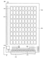
図1及び図2は、本発明の一実施形態に係る表示装置100の構成を示す模式的な平面図である。図1及び図2に示す表示装置100の構成は一例であって、表示装置100の構成は、図1及び図2に示す構成に限定されない。
図3は、本発明の一実施形態に係る画素120の構成を示す平面図である。図4は、本発明の一実施形態に係るサブ画素120Aの回路構成を示す回路図である。図3及び図4は、図2に示したn行m列の画素120の構成を示している。図3及び図4に示す画素120及びサブ画素120Aの構成は一例であって、画素120及びサブ画素120Aの構成は、図3及び図4に示す構成に限定されない。図1及び図2と同一、又は類似する構成については、ここでの説明を省略する。
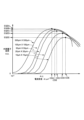
図5は、本発明の一実施形態に係る発光素子の面積に対する量子効率と電流密度の関係を示す模式的な図である。図6は、本発明の一実施形態に係る発光素子の面積に対する量子効率と電流密度の関係を示す模式的な図である。図5及び図6は一例であって、図3及び図4に示すグラフに限定されない。図1~図4と同一、又は類似する構成については、ここでの説明を省略する。

図7は、本発明の一実施形態に係る表示装置100のタイミングチャートを示す模式的な図である。図8~図12は、図7に示すタイミングにおけるサブ画素120Aの第1の発光素子駆動部108Aの動作状態を示す模式的な図である。図13(A)は、本発明の一実施形態に係る表示装置100の第1のサブフレーム期間及び第2のサブフレーム期間の一例を示す図である。図13(B)は、本発明の一実施形態に係る表示装置100の1フレーム(1F)期間の一例を示す図である。図7~図13に示す駆動方法は、本発明の一実施形態に係る表示装置100の駆動方法の一例であって、表示装置100の駆動方法は、図7~図13に示す駆動方法に限定されない。図1~図6と同一、又は類似する構成については、ここでの説明を省略する。
図7に示す第1の期間において、第1の発光素子駆動部108Aは、あるフレーム期間の処理が開始されるまで、あるフレームの1つ前のフレーム期間の動作状態を維持している。
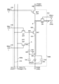
図8は、n行目m列目のサブ画素120Aの第1の発光素子駆動部108Aの図7に示す第2の期間の動作状態を示す。第1リセット信号RG(n)にはHレベルが供給され、発光制御信号BG(n)には、Lレベルが供給される。よって、初期化トランジスタIST、選択トランジスタSST、及び発光制御トランジスタBCTは非導通状態である。一方、リセットトランジスタRSTは導通状態である。なお、駆動トランジスタDRTは、非導通状態であるとするが、導通状態であってもよい。第2の期間では、第1の駆動電源線PVDD1から第1の発光素子RLED1の第1の電極660の方向への電流が発光制御トランジスタBCTによって遮断される。その結果、第1の発光素子RLED1が非発光となると共に、ノードB、ノードCなどに残留していた電荷が駆動トランジスタDRTとリセットトランジスタRSTとを通じて引き抜かれる。その結果、駆動トランジスタDRTのソース電極610が電圧Vrstに固定される。保持容量素子SC1の第1の電極640及びノードAの電圧は、1つ前のフレームで書き込んだ映像信号の電圧である。電圧Vrstは、基準電圧VSSに対して、第1の発光素子RLED1の発光開始電圧よりも低い電圧である。
図9は、n行目m列目のサブ画素120Aの第1の発光素子駆動部108Aの図7に示す第3の期間の動作状態を示す。初期化制御信号IG(n)に供給される電圧がLレベルからHレベルになることに伴い、初期化トランジスタISTが導通状態となる。第3の期間では、初期化トランジスタISTを介して駆動トランジスタDRTのゲート電極620が電圧Viniに固定される。即ち、駆動トランジスタDRTのソース電極610と駆動トランジスタDRTのゲート電極620とがリセット(初期化)される。電圧Viniは、電圧Vrstに対して駆動トランジスタDRTのしきい値電圧よりも大きい電圧に設定される。即ち、駆動トランジスタDRTは導通状態となる。ただし、発光制御トランジスタBCTが非導通状態であるため、第1の駆動電源線PVDD1から第1の発光素子RLED1の第1の電極660の方向への電流は駆動トランジスタDRTに流れない。ノードAの電圧は電圧Viniである。
図10は、n行目m列目のサブ画素120Aの第1の発光素子駆動部108Aの図7に示す第4の期間の動作状態を示す。発光制御信号BG(n)に供給される電圧は、LレベルからHレベルになる。よって、発光制御トランジスタBCTが導通状態となる。また、リセットトランジスタRSTは非導通状態となる。よって、発光制御トランジスタBCTが第1の駆動電源線PVDD1(第1の駆動電源線428)に接続されるため、ノードCの電圧が第1の駆動電源線PVDD1に供給される電圧VDDH1となる。その結果、駆動トランジスタDRTに、第1の駆動電源線PVDD1から第1の発光素子RLED1の第1の電極660の方向への電流が流れる(駆動トランジスタDRTは第2の期間における動作によって導通状態とされている)。したがって、駆動トランジスタDRTのソース電極610及び保持容量素子SC1の第2の電極650が充電される。
図11は、n行目m列目のサブ画素120Aの第1の発光素子駆動部108Aの図7に示す第5の期間の動作状態を示す。第4の期間と第5の期間との間において、初期化制御信号IG(n)に供給される電圧は、HレベルからLレベルになる。よって、初期化トランジスタISTは非導通状態となる。また、第4の期間と第5の期間との間において、走査信号SG(n)に供給される電圧は、LレベルからHレベルになる。よって、選択トランジスタSSTが導通状態となる。映像信号線409aに映像信号SL(m)の電圧Vsig(n)が供給されると、駆動トランジスタDRTのゲート電極620に電圧Vsig(n)が供給され、駆動トランジスタDRTのゲート電極620の電圧が電圧Vsig(n)となる。一方、駆動トランジスタDRTのソース電極610の電圧は(Vini-Vth)である。その結果、駆動トランジスタDRTのゲート電極620とソース電極610との間の電圧が、{Vsig-(Vini-Vth)}となり、発光素子駆動部それぞれの駆動トランジスタDRTのしきい値のばらつきが反映されたものとなる。
図12は、n行目m列目のサブ画素120Aの第1の発光素子駆動部108Aの図7に示す第7の期間の動作状態を示す。第5の期間と第6の期間の間において、走査信号SG(n)に供給される電圧は、HレベルからLレベルになる。よって、選択トランジスタSSTが非導通状態となる。駆動トランジスタDRTは、第5の期間までに設定された駆動トランジスタDRTのゲート電極620とソース電極610との間の電圧(映像信号の電圧)に応じて、第1の駆動電源線PVDD1から第1の発光素子RLED1の第1の電極660の方向に電流を流すことができる。したがって、第1の発光素子RLED1が、駆動トランジスタDRTの流した電流に応じた輝度で発光する。
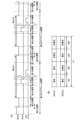
図13(A)に示すように、第1のサブフレーム期間では、発光制御信号BG(n)に供給される電圧がHレベルである時間は、時間BGon1である。第2のサブフレーム期間では、発光制御信号BG(n)に供給される電圧がHレベルである時間は、時間BGon2である。時間BGon1は時間BGon2より短い。発光制御信号BG(n)は発光制御トランジスタBCTの導通状態の時間を制御し、第1の発光素子RLED1及び第2の発光素子RLED2に供給する電流量を制御することができる。その結果、本発明の表示装置100は、複数のサブフレーム期間毎に画素(発光素子)の発光又は非発光の時間を変えることができる。
図14は、本発明の一実施形態に係る表示装置100の断面の一例を示す断面図である。具体的には、図14は、図3に示すサブ画素120AのA1とA2の断面に沿った断面図である。図14に示す断面は、本発明の一実施形態に係る表示装置100の断面の一例であって、表示装置100の断面は、図14に示すに限定されない。図1~図13と同一、又は類似する構成については、ここでの説明を省略する。
Claims (7)
- 第1の方向と、前記第1の方向に交差する第2の方向に配列する複数の画素と、
前記複数の画素のそれぞれに含まれる複数のサブ画素と、
前記複数のサブ画素のうち1つのサブ画素に含まれ、第1の光度L1で発光する第1のLEDチップと、
前記1つのサブ画素に含まれ、第2の光度L2で発光する第2のLEDチップと、
前記第1のLEDチップに、前記第1の光度L1に対応する第1の電圧を供給する第1の配線と、
前記第2のLEDチップに、前記第2の光度L2に対応する第2の電圧を供給する第2の配線と、
を有し、
前記第1のLEDチップと、前記第2のLEDチップとは、同一の色で発光するように構成され、
前記第1のLEDチップの前記第1の光度L1は、前記第1のLEDチップのチップ面積S1及び輝度EQEL1を用いて、式(1)に基づき算出され、
前記第2のLEDチップの前記第2の光度L2は、前記第2のLEDチップのチップ面積S2及び輝度EQEL2を用いて、式(2)に基づき算出され、
前記輝度EQEL1は、外部量子効率が最大値となる電流密度で前記第1のLEDチップが発光するときの前記第1のLEDチップの輝度であり、
前記輝度EQEL2は、外部量子効率が最大値となる電流密度で前記第2のLEDチップが発光するときの前記第2のLEDチップの輝度であり、
前記チップ面積S1は、前記チップ面積S2の2 n 倍(nは1以上の整数)であり、
前記輝度EQEL1における前記第1のLEDチップの電流密度は、前記輝度EQEL2における前記第2のLEDチップの電流密度よりも小さくなるように構成される、表示装置。 - 前記第1の電圧は前記第2の電圧よりも小さい、請求項1に記載の表示装置。
- 前記複数の画素が発光する又は非発光であるフレーム期間は、第1のサブフレーム期間と第2のサブフレーム期間を含み、
前記フレーム期間において、前記第1のLEDチップの発光又は非発光と前記第2のLEDチップの発光又は非発光とは第1の制御信号によって制御される、
請求項1に記載の表示装置。 - 前記第1のサブフレーム期間において、
前記第1のLEDチップが発光するとき、前記第2のLEDチップが発光する又は非発光であり、
前記第1のLEDチップが非発光のとき、前記第2のLEDチップが発光する又は非発光である、
請求項3に記載の表示装置。 - 前記第1のLEDチップが発光している時間又は非発光である時間は、第2の制御信号によって制御され、前記第1のサブフレーム期間と前記第2のサブフレーム期間とにおいて異なり、
前記第2のLEDチップが発光している時間又は非発光である時間は、第3の制御信号によって制御され、前記第1のサブフレーム期間と前記第2のサブフレーム期間とにおいて異なる、
請求項4に記載の表示装置。 - 前記第1のLEDチップと前記第2のLEDチップとはそれぞれが、第1の電極と第2の電極とを有し、
前記第1のLEDチップの第1の電極に供給される電圧と、前記第2のLEDチップの第1の電極に供給される電圧とは異なる、
請求項5に記載の表示装置。 - 前記1つのサブ画素は、第1の容量及び第2の容量を有し、
前記第1の容量の第1の電極は、前記第1のLEDチップの前記第1の電極に接続され、
前記第2の容量の第1の電極は、前記第2のLEDチップの前記第1の電極に接続され、
前記第1のLEDチップの前記第2の電極は前記第2のLEDチップの前記第2の電極に接続され、同一の電圧が供給される、
請求項6に記載の表示装置。
Priority Applications (2)
| Application Number | Priority Date | Filing Date | Title |
|---|---|---|---|
| JP2020086041A JP7561518B2 (ja) | 2020-05-15 | 2020-05-15 | 表示装置 |
| US17/238,216 US11328659B2 (en) | 2020-05-15 | 2021-04-23 | Display device |
Applications Claiming Priority (1)
| Application Number | Priority Date | Filing Date | Title |
|---|---|---|---|
| JP2020086041A JP7561518B2 (ja) | 2020-05-15 | 2020-05-15 | 表示装置 |
Publications (2)
| Publication Number | Publication Date |
|---|---|
| JP2021179571A JP2021179571A (ja) | 2021-11-18 |
| JP7561518B2 true JP7561518B2 (ja) | 2024-10-04 |
Family
ID=78511374
Family Applications (1)
| Application Number | Title | Priority Date | Filing Date |
|---|---|---|---|
| JP2020086041A Active JP7561518B2 (ja) | 2020-05-15 | 2020-05-15 | 表示装置 |
Country Status (2)
| Country | Link |
|---|---|
| US (1) | US11328659B2 (ja) |
| JP (1) | JP7561518B2 (ja) |
Families Citing this family (6)
| Publication number | Priority date | Publication date | Assignee | Title |
|---|---|---|---|---|
| JP7667297B2 (ja) * | 2021-03-04 | 2025-04-22 | アップル インコーポレイテッド | 低減された温度輝度感度を有するディスプレイ |
| CN115602125A (zh) * | 2021-07-08 | 2023-01-13 | 乐金显示有限公司(Kr) | 选通驱动器和使用其的显示装置 |
| CN115425130B (zh) * | 2022-09-06 | 2025-12-16 | 錼创显示科技股份有限公司 | 微型发光二极管显示面板 |
| TWI868480B (zh) * | 2022-09-06 | 2025-01-01 | 錼創顯示科技股份有限公司 | 微型發光二極體顯示面板 |
| WO2025090091A1 (en) * | 2023-10-27 | 2025-05-01 | Google Llc | Extended brightness range of a display |
| US20250336340A1 (en) * | 2024-04-30 | 2025-10-30 | Media Resources Inc. | Systems, devices, and methods for reducing led display brightness |
Citations (2)
| Publication number | Priority date | Publication date | Assignee | Title |
|---|---|---|---|---|
| JP2007041560A (ja) | 2005-07-04 | 2007-02-15 | Semiconductor Energy Lab Co Ltd | 表示装置及び表示装置の駆動方法 |
| US20180190625A1 (en) | 2015-07-07 | 2018-07-05 | Apple Inc. | Quantum dot integration schemes |
Family Cites Families (3)
| Publication number | Priority date | Publication date | Assignee | Title |
|---|---|---|---|---|
| DE102017129981B4 (de) * | 2017-12-14 | 2025-12-04 | OSRAM Opto Semiconductors Gesellschaft mit beschränkter Haftung | Anzeigevorrichtung |
| JP7109957B2 (ja) | 2018-03-27 | 2022-08-01 | 株式会社ジャパンディスプレイ | 表示装置 |
| US11037912B1 (en) * | 2020-01-31 | 2021-06-15 | X Display Company Technology Limited | LED color displays with multiple LEDs connected in series and parallel in different sub-pixels of a pixel |
-
2020
- 2020-05-15 JP JP2020086041A patent/JP7561518B2/ja active Active
-
2021
- 2021-04-23 US US17/238,216 patent/US11328659B2/en active Active
Patent Citations (2)
| Publication number | Priority date | Publication date | Assignee | Title |
|---|---|---|---|---|
| JP2007041560A (ja) | 2005-07-04 | 2007-02-15 | Semiconductor Energy Lab Co Ltd | 表示装置及び表示装置の駆動方法 |
| US20180190625A1 (en) | 2015-07-07 | 2018-07-05 | Apple Inc. | Quantum dot integration schemes |
Also Published As
| Publication number | Publication date |
|---|---|
| US11328659B2 (en) | 2022-05-10 |
| JP2021179571A (ja) | 2021-11-18 |
| US20210358392A1 (en) | 2021-11-18 |
Similar Documents
| Publication | Publication Date | Title |
|---|---|---|
| JP7561518B2 (ja) | 表示装置 | |
| US11908409B2 (en) | Display apparatus | |
| US8004480B2 (en) | Organic light emitting display | |
| US11545076B2 (en) | Display device having a reset line for supplying a reset signal | |
| CN111326673B (zh) | 显示装置 | |
| JP6996855B2 (ja) | 表示装置の駆動方法 | |
| KR20020077138A (ko) | 표시장치 | |
| CN101261805A (zh) | 有机电致发光显示器 | |
| JP7261071B2 (ja) | 表示装置 | |
| JP4776328B2 (ja) | 発光表示パネル,発光表示装置および発光表示装置の駆動方法 | |
| US12062333B2 (en) | Pixel and display device including the same | |
| JP6116186B2 (ja) | 表示装置 | |
| JP7362742B2 (ja) | 表示装置 | |
| CN114551514A (zh) | 透明显示装置 | |
| TWI898354B (zh) | 顯示裝置 | |
| JP6186127B2 (ja) | 表示装置 | |
| JP2009115840A (ja) | アクティブマトリクス型表示装置及びアクティブマトリクス型表示装置の駆動方法 | |
| US20250265989A1 (en) | Micro display device | |
| JP5442678B2 (ja) | 表示装置 | |
| CN116437754A (zh) | 有机发光显示面板 |
Legal Events
| Date | Code | Title | Description |
|---|---|---|---|
| A621 | Written request for application examination |
Free format text: JAPANESE INTERMEDIATE CODE: A621 Effective date: 20230512 |
|
| A977 | Report on retrieval |
Free format text: JAPANESE INTERMEDIATE CODE: A971007 Effective date: 20240117 |
|
| A131 | Notification of reasons for refusal |
Free format text: JAPANESE INTERMEDIATE CODE: A131 Effective date: 20240305 |
|
| A601 | Written request for extension of time |
Free format text: JAPANESE INTERMEDIATE CODE: A601 Effective date: 20240430 |
|
| A521 | Request for written amendment filed |
Free format text: JAPANESE INTERMEDIATE CODE: A523 Effective date: 20240611 |
|
| TRDD | Decision of grant or rejection written | ||
| A01 | Written decision to grant a patent or to grant a registration (utility model) |
Free format text: JAPANESE INTERMEDIATE CODE: A01 Effective date: 20240903 |
|
| A61 | First payment of annual fees (during grant procedure) |
Free format text: JAPANESE INTERMEDIATE CODE: A61 Effective date: 20240924 |
|
| R150 | Certificate of patent or registration of utility model |
Ref document number: 7561518 Country of ref document: JP Free format text: JAPANESE INTERMEDIATE CODE: R150 |