JP7561518B2 - Display device - Google Patents
Display device Download PDFInfo
- Publication number
- JP7561518B2 JP7561518B2 JP2020086041A JP2020086041A JP7561518B2 JP 7561518 B2 JP7561518 B2 JP 7561518B2 JP 2020086041 A JP2020086041 A JP 2020086041A JP 2020086041 A JP2020086041 A JP 2020086041A JP 7561518 B2 JP7561518 B2 JP 7561518B2
- Authority
- JP
- Japan
- Prior art keywords
- light
- emitting element
- electrode
- led chip
- voltage
- Prior art date
- Legal status (The legal status is an assumption and is not a legal conclusion. Google has not performed a legal analysis and makes no representation as to the accuracy of the status listed.)
- Active
Links
Images


Classifications
-
- G—PHYSICS
- G09—EDUCATION; CRYPTOGRAPHY; DISPLAY; ADVERTISING; SEALS
- G09G—ARRANGEMENTS OR CIRCUITS FOR CONTROL OF INDICATING DEVICES USING STATIC MEANS TO PRESENT VARIABLE INFORMATION
- G09G3/00—Control arrangements or circuits, of interest only in connection with visual indicators other than cathode-ray tubes
- G09G3/20—Control arrangements or circuits, of interest only in connection with visual indicators other than cathode-ray tubes for presentation of an assembly of a number of characters, e.g. a page, by composing the assembly by combination of individual elements arranged in a matrix no fixed position being assigned to or needed to be assigned to the individual characters or partial characters
- G09G3/22—Control arrangements or circuits, of interest only in connection with visual indicators other than cathode-ray tubes for presentation of an assembly of a number of characters, e.g. a page, by composing the assembly by combination of individual elements arranged in a matrix no fixed position being assigned to or needed to be assigned to the individual characters or partial characters using controlled light sources
- G09G3/30—Control arrangements or circuits, of interest only in connection with visual indicators other than cathode-ray tubes for presentation of an assembly of a number of characters, e.g. a page, by composing the assembly by combination of individual elements arranged in a matrix no fixed position being assigned to or needed to be assigned to the individual characters or partial characters using controlled light sources using electroluminescent panels
- G09G3/32—Control arrangements or circuits, of interest only in connection with visual indicators other than cathode-ray tubes for presentation of an assembly of a number of characters, e.g. a page, by composing the assembly by combination of individual elements arranged in a matrix no fixed position being assigned to or needed to be assigned to the individual characters or partial characters using controlled light sources using electroluminescent panels semiconductive, e.g. using light-emitting diodes [LED]
-
- G—PHYSICS
- G09—EDUCATION; CRYPTOGRAPHY; DISPLAY; ADVERTISING; SEALS
- G09G—ARRANGEMENTS OR CIRCUITS FOR CONTROL OF INDICATING DEVICES USING STATIC MEANS TO PRESENT VARIABLE INFORMATION
- G09G3/00—Control arrangements or circuits, of interest only in connection with visual indicators other than cathode-ray tubes
- G09G3/20—Control arrangements or circuits, of interest only in connection with visual indicators other than cathode-ray tubes for presentation of an assembly of a number of characters, e.g. a page, by composing the assembly by combination of individual elements arranged in a matrix no fixed position being assigned to or needed to be assigned to the individual characters or partial characters
- G09G3/2007—Display of intermediate tones
- G09G3/2018—Display of intermediate tones by time modulation using two or more time intervals
- G09G3/2022—Display of intermediate tones by time modulation using two or more time intervals using sub-frames
-
- G—PHYSICS
- G09—EDUCATION; CRYPTOGRAPHY; DISPLAY; ADVERTISING; SEALS
- G09G—ARRANGEMENTS OR CIRCUITS FOR CONTROL OF INDICATING DEVICES USING STATIC MEANS TO PRESENT VARIABLE INFORMATION
- G09G3/00—Control arrangements or circuits, of interest only in connection with visual indicators other than cathode-ray tubes
- G09G3/20—Control arrangements or circuits, of interest only in connection with visual indicators other than cathode-ray tubes for presentation of an assembly of a number of characters, e.g. a page, by composing the assembly by combination of individual elements arranged in a matrix no fixed position being assigned to or needed to be assigned to the individual characters or partial characters
- G09G3/2007—Display of intermediate tones
- G09G3/207—Display of intermediate tones by domain size control
-
- G—PHYSICS
- G09—EDUCATION; CRYPTOGRAPHY; DISPLAY; ADVERTISING; SEALS
- G09G—ARRANGEMENTS OR CIRCUITS FOR CONTROL OF INDICATING DEVICES USING STATIC MEANS TO PRESENT VARIABLE INFORMATION
- G09G3/00—Control arrangements or circuits, of interest only in connection with visual indicators other than cathode-ray tubes
- G09G3/20—Control arrangements or circuits, of interest only in connection with visual indicators other than cathode-ray tubes for presentation of an assembly of a number of characters, e.g. a page, by composing the assembly by combination of individual elements arranged in a matrix no fixed position being assigned to or needed to be assigned to the individual characters or partial characters
- G09G3/2007—Display of intermediate tones
- G09G3/2077—Display of intermediate tones by a combination of two or more gradation control methods
- G09G3/2081—Display of intermediate tones by a combination of two or more gradation control methods with combination of amplitude modulation and time modulation
-
- H—ELECTRICITY
- H10—SEMICONDUCTOR DEVICES; ELECTRIC SOLID-STATE DEVICES NOT OTHERWISE PROVIDED FOR
- H10W—GENERIC PACKAGES, INTERCONNECTIONS, CONNECTORS OR OTHER CONSTRUCTIONAL DETAILS OF DEVICES COVERED BY CLASS H10
- H10W90/00—Package configurations
-
- G—PHYSICS
- G09—EDUCATION; CRYPTOGRAPHY; DISPLAY; ADVERTISING; SEALS
- G09G—ARRANGEMENTS OR CIRCUITS FOR CONTROL OF INDICATING DEVICES USING STATIC MEANS TO PRESENT VARIABLE INFORMATION
- G09G2300/00—Aspects of the constitution of display devices
- G09G2300/04—Structural and physical details of display devices
- G09G2300/0421—Structural details of the set of electrodes
- G09G2300/0426—Layout of electrodes and connections
-
- G—PHYSICS
- G09—EDUCATION; CRYPTOGRAPHY; DISPLAY; ADVERTISING; SEALS
- G09G—ARRANGEMENTS OR CIRCUITS FOR CONTROL OF INDICATING DEVICES USING STATIC MEANS TO PRESENT VARIABLE INFORMATION
- G09G2300/00—Aspects of the constitution of display devices
- G09G2300/04—Structural and physical details of display devices
- G09G2300/0439—Pixel structures
- G09G2300/0452—Details of colour pixel setup, e.g. pixel composed of a red, a blue and two green components
-
- G—PHYSICS
- G09—EDUCATION; CRYPTOGRAPHY; DISPLAY; ADVERTISING; SEALS
- G09G—ARRANGEMENTS OR CIRCUITS FOR CONTROL OF INDICATING DEVICES USING STATIC MEANS TO PRESENT VARIABLE INFORMATION
- G09G2300/00—Aspects of the constitution of display devices
- G09G2300/08—Active matrix structure, i.e. with use of active elements, inclusive of non-linear two terminal elements, in the pixels together with light emitting or modulating elements
- G09G2300/0809—Several active elements per pixel in active matrix panels
- G09G2300/0819—Several active elements per pixel in active matrix panels used for counteracting undesired variations, e.g. feedback or autozeroing
-
- G—PHYSICS
- G09—EDUCATION; CRYPTOGRAPHY; DISPLAY; ADVERTISING; SEALS
- G09G—ARRANGEMENTS OR CIRCUITS FOR CONTROL OF INDICATING DEVICES USING STATIC MEANS TO PRESENT VARIABLE INFORMATION
- G09G2300/00—Aspects of the constitution of display devices
- G09G2300/08—Active matrix structure, i.e. with use of active elements, inclusive of non-linear two terminal elements, in the pixels together with light emitting or modulating elements
- G09G2300/0809—Several active elements per pixel in active matrix panels
- G09G2300/0842—Several active elements per pixel in active matrix panels forming a memory circuit, e.g. a dynamic memory with one capacitor
- G09G2300/0861—Several active elements per pixel in active matrix panels forming a memory circuit, e.g. a dynamic memory with one capacitor with additional control of the display period without amending the charge stored in a pixel memory, e.g. by means of additional select electrodes
-
- G—PHYSICS
- G09—EDUCATION; CRYPTOGRAPHY; DISPLAY; ADVERTISING; SEALS
- G09G—ARRANGEMENTS OR CIRCUITS FOR CONTROL OF INDICATING DEVICES USING STATIC MEANS TO PRESENT VARIABLE INFORMATION
- G09G2310/00—Command of the display device
- G09G2310/02—Addressing, scanning or driving the display screen or processing steps related thereto
- G09G2310/0264—Details of driving circuits
- G09G2310/0267—Details of drivers for scan electrodes, other than drivers for liquid crystal, plasma or OLED displays
-
- G—PHYSICS
- G09—EDUCATION; CRYPTOGRAPHY; DISPLAY; ADVERTISING; SEALS
- G09G—ARRANGEMENTS OR CIRCUITS FOR CONTROL OF INDICATING DEVICES USING STATIC MEANS TO PRESENT VARIABLE INFORMATION
- G09G2320/00—Control of display operating conditions
- G09G2320/02—Improving the quality of display appearance
- G09G2320/0242—Compensation of deficiencies in the appearance of colours
-
- G—PHYSICS
- G09—EDUCATION; CRYPTOGRAPHY; DISPLAY; ADVERTISING; SEALS
- G09G—ARRANGEMENTS OR CIRCUITS FOR CONTROL OF INDICATING DEVICES USING STATIC MEANS TO PRESENT VARIABLE INFORMATION
- G09G2320/00—Control of display operating conditions
- G09G2320/04—Maintaining the quality of display appearance
- G09G2320/043—Preventing or counteracting the effects of ageing
- G09G2320/045—Compensation of drifts in the characteristics of light emitting or modulating elements
-
- G—PHYSICS
- G09—EDUCATION; CRYPTOGRAPHY; DISPLAY; ADVERTISING; SEALS
- G09G—ARRANGEMENTS OR CIRCUITS FOR CONTROL OF INDICATING DEVICES USING STATIC MEANS TO PRESENT VARIABLE INFORMATION
- G09G2320/00—Control of display operating conditions
- G09G2320/06—Adjustment of display parameters
- G09G2320/0626—Adjustment of display parameters for control of overall brightness
- G09G2320/064—Adjustment of display parameters for control of overall brightness by time modulation of the brightness of the illumination source
-
- G—PHYSICS
- G09—EDUCATION; CRYPTOGRAPHY; DISPLAY; ADVERTISING; SEALS
- G09G—ARRANGEMENTS OR CIRCUITS FOR CONTROL OF INDICATING DEVICES USING STATIC MEANS TO PRESENT VARIABLE INFORMATION
- G09G2360/00—Aspects of the architecture of display systems
- G09G2360/16—Calculation or use of calculated indices related to luminance levels in display data
-
- H—ELECTRICITY
- H10—SEMICONDUCTOR DEVICES; ELECTRIC SOLID-STATE DEVICES NOT OTHERWISE PROVIDED FOR
- H10H—INORGANIC LIGHT-EMITTING SEMICONDUCTOR DEVICES HAVING POTENTIAL BARRIERS
- H10H20/00—Individual inorganic light-emitting semiconductor devices having potential barriers, e.g. light-emitting diodes [LED]
- H10H20/80—Constructional details
- H10H20/81—Bodies
- H10H20/819—Bodies characterised by their shape, e.g. curved or truncated substrates
-
- H—ELECTRICITY
- H10—SEMICONDUCTOR DEVICES; ELECTRIC SOLID-STATE DEVICES NOT OTHERWISE PROVIDED FOR
- H10H—INORGANIC LIGHT-EMITTING SEMICONDUCTOR DEVICES HAVING POTENTIAL BARRIERS
- H10H20/00—Individual inorganic light-emitting semiconductor devices having potential barriers, e.g. light-emitting diodes [LED]
- H10H20/80—Constructional details
- H10H20/85—Packages
- H10H20/857—Interconnections, e.g. lead-frames, bond wires or solder balls
Landscapes
- Engineering & Computer Science (AREA)
- Physics & Mathematics (AREA)
- Computer Hardware Design (AREA)
- General Physics & Mathematics (AREA)
- Theoretical Computer Science (AREA)
- Control Of Indicators Other Than Cathode Ray Tubes (AREA)
- Electroluminescent Light Sources (AREA)
- Devices For Indicating Variable Information By Combining Individual Elements (AREA)
- Control Of El Displays (AREA)
- Led Devices (AREA)
Description
本発明は表示装置に関する。 The present invention relates to a display device.
近年、複数の画素のそれぞれを発光素子で形成した表示装置が注目されている。発光素子は、例えば、発光ダイオード(Light Emitting Diode:LED)、微小な発光ダイオード(マイクロLED)、有機エレクトロルミネッセンス(Electro Luminescence:EL)素子等である。発光素子の発光強度又は輝度は、発光素子を流れる電流値で制御される。複数の画素を発光素子で形成した表示装置において、階調を表示する技術の1つが面積階調技術である。 In recent years, display devices in which multiple pixels are each formed from a light-emitting element have been attracting attention. Light-emitting elements include, for example, light-emitting diodes (LEDs), tiny light-emitting diodes (micro LEDs), and organic electroluminescence (EL) elements. The light-emitting intensity or brightness of the light-emitting element is controlled by the value of the current flowing through the light-emitting element. In display devices in which multiple pixels are formed from light-emitting elements, one of the technologies for displaying gradations is area gradation technology.
例えば、引用文献1は、複数の画素のそれぞれが面積の異なる2つの有機EL素子を有する表示装置を開示している。また、引用文献1に記載の表示装置では、階調を表示する技術として、面積の異なる2つの有機EL素子のそれぞれにおいて、発光と非発光とを制御し、有機EL素子の発光する面積を変える面積階調技術を開示している。
For example,
表示装置を構成する発光素子が、例えば、マイクロLEDを含むLEDの場合、LEDの最適な量子効率は、LEDのサイズによって異なる。例えば、複数の面積の異なるLEDを同一の電流密度で駆動すると、色度に差が生じる可能性がある。その結果、複数のLEDの寿命の差が、表示装置の長期信頼性に影響を及ぼす可能性がある。 When the light-emitting elements constituting the display device are, for example, LEDs including micro LEDs, the optimal quantum efficiency of the LEDs varies depending on the size of the LEDs. For example, when multiple LEDs with different areas are driven at the same current density, differences in chromaticity may occur. As a result, differences in the life spans of multiple LEDs may affect the long-term reliability of the display device.
このような課題に鑑み、本発明の一実施形態は、長期信頼性の低下を軽減する表示装置を提供することを目的の一つとする。 In view of these issues, one embodiment of the present invention aims to provide a display device that reduces the deterioration of long-term reliability.
本発明の一実施形態は、表示装置であって、第1の方向と、第1の方向に交差する第2の方向に配列する複数の画素と、複数の画素のそれぞれに含まれる複数のサブ画素と、複数のサブ画素のうち1つのサブ画素に含まれ、第1の光度で発光する第1のLEDチップと、1つのサブ画素に含まれ、第2の光度L2で発光する第2のLEDチップと、第1のLEDチップに、第1の光度L1に対応する第1の電圧を供給する第1の配線と、第2のLEDチップに、第2の光度L2に対応する第2の電圧を供給する第2の配線と、を有し、第1のLEDチップの第1の光度L1は、第1のLEDチップのチップ面積S1及び輝度EQEL1を用いて、式(1)に基づき算出され、
![]()
![]()
![]()
![]()
以下、本発明の実施形態を、図面等を参照しながら説明する。但し、本発明は多くの異なる態様で実施することが可能であり、以下に例示する実施の形態の記載内容に限定して解釈されるものではない。 Embodiments of the present invention will be described below with reference to the drawings. However, the present invention can be implemented in many different ways, and should not be interpreted as being limited to the description of the embodiments exemplified below.
また、図面は説明をより明確にするため、実際の態様に比べ、各部の構成等について模式的に表される場合があるが、あくまで一例であって、本発明の解釈を限定するものではない。 In addition, in order to make the explanation clearer, the drawings may show the configuration of each part more diagrammatically than in the actual embodiment, but this is merely an example and does not limit the interpretation of the present invention.
さらに、本明細書と各図において、既出の図に関して前述したものと同様の要素には、同一の符号(又は数字の後にa、b、A,Bなどを付した符号)を付して、詳細な説明を適宜省略することがある。なお、各要素に対する「第1」、「第2」と付記された文字は、各要素を区別するために用いられる便宜的な標識であり、特段の説明がない限りそれ以上の意味を有さない。 Furthermore, in this specification and each figure, elements similar to those previously described with respect to the previous figures may be given the same reference numerals (or numerals followed by a, b, A, B, etc.) and detailed explanations may be omitted as appropriate. Note that the letters "first" and "second" attached to each element are convenient labels used to distinguish each element and have no other meaning unless otherwise specified.
また、本明細書において、ある部材又は領域が他の部材又は領域の「上に(又は下に)」あるとすることができる。特段の限定がない限りこれは他の部材又は領域の直上(又は直下)にある場合のみでなく他の部材又は領域の上方(又は下方)にある場合を含み、すなわち、他の部材又は領域の上方(又は下方)において間に別の構成要素が含まれている場合も含む。なお、以下の説明では、特に断りのない限り、断面視においては、基板に対して発光素子が配置される側を「上」又は「上面」といい、その逆を「下」又は「下面」として説明する。 Furthermore, in this specification, a certain component or region can be said to be "above (or below)" another component or region. Unless otherwise specified, this includes not only the case where it is directly above (or below) another component or region, but also the case where it is above (or below) the other component or region, that is, the case where another component is included between the other component or region and above (or below) it. In the following description, unless otherwise specified, in a cross-sectional view, the side on which the light-emitting element is arranged with respect to the substrate will be referred to as "above" or "upper surface", and the opposite will be referred to as "below" or "lower surface".
また、本明細書において「αはA、B又はCを含む」、「αはA,B及びCのいずれかを含む」、「αはA,B及びCからなる群から選択される一つを含む」、といった表現は、特に明示が無い限り、αはA~Cの複数の組み合わせを含む場合を排除しない。さらに、これらの表現は、αが他の要素を含む場合も排除しない。 Furthermore, in this specification, expressions such as "α includes A, B, or C," "α includes any of A, B, and C," and "α includes one selected from the group consisting of A, B, and C" do not exclude cases where α includes multiple combinations of A through C, unless otherwise specified. Furthermore, these expressions do not exclude cases where α includes other elements.
本明細書において説明される基板は、少なくとも平面状の一主面を有し、この一主面上に絶縁層、半導体層及び導電層の各層、或いはトランジスタ及び発光素子等の各素子が設けられる。以下の説明では、断面視において、基板の一主面を基準にして述べるものとする。 The substrate described in this specification has at least one planar main surface, on which insulating layers, semiconductor layers, and conductive layers, or elements such as transistors and light-emitting elements, are provided. In the following description, the cross-sectional view will be described with reference to the main surface of the substrate.
本願の明細書及び特許請求の範囲(以下「本明細書等」という。)において、実施形態の1つである表示装置は、一例として、発光素子にマイクロLEDを用いる表示装置である。 In the specification and claims of this application (hereinafter referred to as "this specification"), one embodiment of the display device is, as an example, a display device that uses micro LEDs as light-emitting elements.
<1.表示装置100の全体構成>
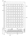
図1及び図2は、本発明の一実施形態に係る表示装置100の構成を示す模式的な平面図である。図1及び図2に示す表示装置100の構成は一例であって、表示装置100の構成は、図1及び図2に示す構成に限定されない。
1. Overall configuration of the
1 and 2 are schematic plan views showing a configuration of a
図1に示すように、表示装置100は、基板502、表示部504、映像信号線駆動回路506、走査信号線駆動回路510、制御回路518、端子電極514、及び周辺領域516を有する。表示部504、映像信号線駆動回路506、走査信号線駆動回路510、制御回路518、端子電極514、及び周辺領域516は、基板502の上面に設ける。表示部504は、表示装置100に映像を表示するための複数の画素120を有する。
As shown in FIG. 1, the
複数の画素120は、x方向と、x方向に交差するy方向にマトリクス状に配列する。複数の画素120のそれぞれは、複数のサブ画素(図4)を含み、複数のサブ画素のそれぞれは、少なくとも、トランジスタ(図4)及び第1の発光素子(図4)及び第2の発光素子(図4)を有する。第1の発光素子は第1の光度で発光し、第2の発光素子は第2の光度で発光する。第2の発光素子の面積は第1の発光素子の面積よりも小さい。本発明の一実施形態に係る表示装置100は、トランジスタを駆動し、LEDを発光又は非発光することで、表示部504に映像を表示することができる。本明細書等において、例えば、x方向は第1の方向と呼ばれ、y方向は第2の方向と呼ばれ、発光素子はLEDチップと呼ばれる。なお、画素120、サブ画素、及び発光素子の詳細は、後述する。
The
周辺領域516には、画素120の駆動を制御するための走査信号線駆動回路510及び映像信号線駆動回路506が設けられる。図1においては、映像信号線駆動回路506はICチップを用いる例を示す。また、図2においては、走査信号線駆動回路510及び映像信号線駆動回路506は基板502の上面に設ける例を示す。走査信号線駆動回路510及び映像信号線駆動回路506は図1及び図2で示される例に限定されない。走査信号線駆動回路510及び映像信号線駆動回路506は、例えば、基板502とは異なる基板(半導体基板など)の上に形成された駆動回路を、基板502やフレキシブルプリント回路(FPC、FlexiblePrintedCircuit)基板などのコネクタ512の上に設けてもよい。また、走査信号線駆動回路510及び映像信号線駆動回路506が有する回路の一部又は全部を基板502とは異なる基板の上に形成し、基板502やコネクタ512の上に設ける構成としてもよい。また、映像信号線駆動回路506に含まれる駆動回路又は駆動回路の一部が、基板502の上に直接形成されてもよい。詳細は後述するが、基板502の上面には、画素120内に設けられる発光素子(LED)、及び、発光素子を制御するための各種半導体素子が形成される。
In the
また、表示装置100は、第1の配線206、コンタクトホール208、第1の電極配線210、第1の電極212、第2の配線216、コンタクトホール218、第2の電極配線220、第2の電極222を有する。これらは、走査信号線駆動回路510と同様に、基板502の上面に設ける。
The
図1において図示は省略するが、例えば、各画素120に映像信号を供給するための映像信号線、各画素120に電源を供給するための電源線、走査信号線駆動回路510、及び制御回路518が、表示部504の外から延びる第1の配線206と電気的に接続される。第1の配線206は表示部504の外を延伸し、コンタクトホール208を介して第1の電極配線210と電気的に接続される。第1の電極配線210は表示装置100の端部付近で露出され、第1の電極212を形成する。第1の電極212はコネクタ512と接続される。
Although not shown in FIG. 1, for example, a video signal line for supplying a video signal to each
図1において図示は省略するが、同様にして、例えば、各画素120に映像信号を供給するための映像信号線、各画素120に電源を供給するための電源線、走査信号線駆動回路510、及び制御回路518が、表示部504の外から延びる第2の配線216と電気的に接続される。第2の配線216は表示部504の外を延伸し、コンタクトホール218を介して第2の電極配線220と電気的に接続される。第2の電極配線220は表示装置100の端部付近で露出され、第2の電極222を形成する。第2の電極222はコネクタ512と接続される。なお、第2の配線216は第1の配線206であってもよい。コンタクトホール218はコンタクトホール208であってもよい。第2の電極配線220は第1の電極配線210であってもよい。第2の電極222は第1の電極配線210であってもよい。第2の電極222は第1の電極212であってもよい。
1, for example, a video signal line for supplying a video signal to each
各信号及び電源は、外部回路(図示は省略)から第1の電極212、走査信号線駆動回路510及び映像信号線駆動回路506を経由して、画素120に供給される。第1の電極212は、表示装置100の一つの辺に並ぶように形成することができる。このため、単一のコネクタ512を用いて、表示部504に、独立して、電圧や信号を供給することができる。
Each signal and power source is supplied to the
図2に示されるように、制御回路518は、外部回路(図示は省略)から複数の端子電極514(図1)を介して、映像信号、回路の動作を制御するタイミング信号、電源などを供給される。制御回路518は、各信号や電源電圧などを、走査信号線駆動回路510や映像信号線駆動回路506に供給する。制御回路518は、制御回路518が有する論理回路(図示せず)や電圧生成回路(図示せず)を用いて、各信号や電源電圧などから新たな信号や電源電圧を生成し、走査信号線駆動回路510や映像信号線駆動回路506に供給してもよい。制御回路518が配置される位置は、図1に示す基板502上に限定されない。例えば、制御回路518は、端子電極514に接続されたコネクタ512上に位置してもよい。
2, the
走査信号線駆動回路510及び映像信号線駆動回路506は、制御回路518から供給される各信号や電源電圧を用いて、画素120が有するトランジスタ(図4)を駆動し、LED(図4)を発光または非発光することで、表示部504に映像を表示する役割を果たす。
The scanning signal
走査信号線駆動回路510は、表示部504内のn行目に位置する複数の画素120に、共通に、走査信号SG(n)と、発光制御信号BG(n)と、初期化制御信号IG(n)と、第1リセット信号RG(n)とを供給する。ここで、第1リセット信号RG(n)は、表示部504内のn行目に位置する複数の画素120に、電圧Vrstを供給する。基準電位線PVSSは、複数の画素120に、共通に、基準電位VSSを供給する。リセット信号VL1は、複数の画素120に、共通に、電圧Vrstを供給する。
The scanning signal
映像信号線駆動回路506は、表示部504内のm列目に位置する複数の画素120に、共通に、映像信号SL(m)と、第2リセット信号VL2とを供給する。ここで、第2リセット信号VL2は、表示部504内のm列目に位置する複数の画素120に、電圧Viniを供給する。第1の駆動電源線PVDD1は、表示部504内のm列目に位置する複数の画素120に、第1の駆動電圧VDDH1を供給する。第2の駆動電源線PVDD2は、表示部504内のm列目に位置する複数の画素120に、第2の駆動電圧VDDH2を供給する。第3の駆動電源線PVDD3は、表示部504内のm列目に位置する複数の画素120に、第3の駆動電圧VDDH3を供給する。第4の駆動電源線PVDD4は、表示部504内のm列目に位置する複数の画素120に、第4の駆動電圧VDDH4を供給する。第5の駆動電源線PVDD5は、表示部504内のm列目に位置する複数の画素120に、第5の駆動電圧VDDH5を供給する。第6の駆動電源線PVDD6は、表示部504内のm列目に位置する複数の画素120に、第6の駆動電圧VDDH6を供給する。以下、映像信号の電圧をVsig(m)、又はVsig(n)と呼ぶ。映像信号は、表示部504で表示される映像データに基づき決定される。本明細書等において、数値mは12以上の任意の整数である。本明細書等において、数値nは1以上の任意の整数である。また、本明細書等において、第1の駆動電源線PVDD1、第3の駆動電源線PVDD3、第5の駆動電源線PVDD5を第1の配線、第2の駆動電源線PVDD2、第4の駆動電源線PVDD4、第6の駆動電源線PVDD6を第2の配線と呼ぶ場合がある。
The video signal
本明細書等においては、電圧Vrst及び電圧Viniが固定電圧である例を示すが、電圧Vrst及び電圧Viniは時間経過とともに変化してもよい。また、本明細書等においては、走査信号線駆動回路510が、複数の画素120に、第1リセット信号RGを供給し、映像信号線駆動回路506が、複数の画素120に、第2リセット信号VL2を供給する例を示すが、この例に限定されない。映像信号線駆動回路506が、複数の画素120に、第1リセット信号RGを供給してもよく、走査信号線駆動回路510が、複数の画素120に、第2リセット信号VL2を供給してもよい。また、走査信号線駆動回路510と映像信号線駆動回路506の何れか一方が、複数の画素120に、第1リセット信号RG及び第2リセット信号VL2を供給してもよい。また、第1リセット信号RG及び第2リセット信号線VL2は、端子電極514に電気的に接続されてもよい。このとき、電圧Vrst及び電圧Viniは、表示装置100の外部に設けられる外部装置(図示は省略)からコネクタ512を介して供給される。本明細書等において、電圧Vrstはリセット電圧と呼ぶことがある。また、本明細書等において、電圧Viniは初期化電圧と呼ぶことがある。
In this specification, an example is shown in which the voltages Vrst and Vini are fixed voltages, but the voltages Vrst and Vini may change over time. In this specification, an example is shown in which the scanning signal
また、本明細書等においては、第1の駆動電源線PVDD1、第2の駆動電源線PVDD2、第3の駆動電源線PVDD3、第4の駆動電源線PVDD4、第5の駆動電源線PVDD5、及び第6の駆動電源線PVDD6は、映像信号線駆動回路506に設けられ、第1の駆動電圧VDDH1、第2の駆動電圧VDDH2、第3の駆動電圧VDDH3、第4の駆動電圧VDDH4、第5の駆動電圧VDDH5及び第6の駆動電圧VDDH6は、映像信号線駆動回路506から各画素120に供給する例を示すが、この例に限定されない。第1の駆動電源線PVDD1、第2の駆動電源線PVDD2、第3の駆動電源線PVDD3、第4の駆動電源線PVDD4、第5の駆動電源線PVDD5、及び第6の駆動電源線PVDD6は、走査信号線駆動回路510に設けられてもよく、第1の駆動電圧VDDH1、第2の駆動電圧VDDH2、第3の駆動電圧VDDH3、第4の駆動電圧VDDH4、第5の駆動電圧VDDH5及び第6の駆動電圧VDDH6の一部が走査信号線駆動回路510に設けられ、一部以外が映像信号線駆動回路506に設けられてもよい。本発明の一実施係る表示装置100においては、用途、仕様等に合わせて、電源線の配置を適宜変えてもよい。
Furthermore, in this specification, an example is shown in which the first drive power line PVDD1, the second drive power line PVDD2, the third drive power line PVDD3, the fourth drive power line PVDD4, the fifth drive power line PVDD5, and the sixth drive power line PVDD6 are provided in the video signal
<2.画素120の構成>
図3は、本発明の一実施形態に係る画素120の構成を示す平面図である。図4は、本発明の一実施形態に係るサブ画素120Aの回路構成を示す回路図である。図3及び図4は、図2に示したn行m列の画素120の構成を示している。図3及び図4に示す画素120及びサブ画素120Aの構成は一例であって、画素120及びサブ画素120Aの構成は、図3及び図4に示す構成に限定されない。図1及び図2と同一、又は類似する構成については、ここでの説明を省略する。
2. Configuration of
Fig. 3 is a plan view showing a configuration of a
図3に示すように、画素120は、例えば、サブ画素120A、サブ画素120B、及びサブ画素120Cを有する。
As shown in FIG. 3,
サブ画素120Aは、第1の発光素子RLED1及び第2の発光素子RLED2を有する。第1の発光素子RLED1及び第2の発光素子RLED2は赤色発光ダイオードである。第1の発光素子RLED1及び第2の発光素子RLED2の形状は、例えば、正四角形である。第1の発光素子RLED1の長辺及び短辺は、長さa及び短辺bであり、第1の発光素子RLED1の面積は、面積a×bである。第2の発光素子RLED2の長辺及び短辺は、長さc及び短辺dであり、第2の発光素子RLED2の面積は、面積c×dである。面積c×dは、面積a×bよりも小さく、面積a×bは面積c×dの2倍又はおよそ2倍である。第1の発光素子RLED1のチップ面積は第2の発光素子RLED2のチップ面積の2 n 倍(nは1以上の整数)であってよい。この場合、第1の発光素子RLED1と第2の発光素子RLED2とは、その輝度が同等であり、チップ面積の比率に応じた光度が得られるものとする。 The sub-pixel 120A has a first light-emitting element RLED1 and a second light-emitting element RLED2. The first light-emitting element RLED1 and the second light-emitting element RLED2 are red light-emitting diodes. The shapes of the first light-emitting element RLED1 and the second light-emitting element RLED2 are, for example, regular rectangles. The long and short sides of the first light-emitting element RLED1 have a length a and a short side b, and the area of the first light-emitting element RLED1 is an area a×b. The long and short sides of the second light-emitting element RLED2 have a length c and a short side d, and the area of the second light-emitting element RLED2 is an area c×d. The area c×d is smaller than the area a×b, and the area a×b is twice or approximately twice the area c×d. The chip area of the first light-emitting element RLED1 may be 2 n times (n is an integer of 1 or more) the chip area of the second light-emitting element RLED2. In this case, the first light emitting element RLED1 and the second light emitting element RLED2 have the same luminance, and a luminous intensity according to the ratio of the chip areas is obtained.
サブ画素120Bは、第1の発光素子GLED1及び第2の発光素子GLED2を有する。第1の発光素子GLED1及び第2の発光素子GLED2は緑色発光ダイオードである。第1の発光素子GLED1及び第2の発光素子GLED2の形状は、例えば、正四角形である。第1の発光素子GLED1の長辺及び短辺は、長さe及び短辺fであり、第1の発光素子GLED1の面積は、面積e×fである。第2の発光素子GLED2の長辺及び短辺は、長さg及び短辺hであり、第2の発光素子GLED2の面積は、面積g×hである。面積g×hは、面積e×fよりも小さく、面積e×fは面積g×hの2倍又はおよそ2倍である。第1の発光素子GLED1のチップ面積は第2の発光素子GLED2のチップ面積の2 n 倍であってよい。この場合、第1の発光素子GLED1と第2の発光素子GLED2とは、その輝度が同等であり、チップ面積の比率に応じた光度がえられるものとする。 The sub-pixel 120B has a first light-emitting element GLED1 and a second light-emitting element GLED2. The first light-emitting element GLED1 and the second light-emitting element GLED2 are green light-emitting diodes. The shapes of the first light-emitting element GLED1 and the second light-emitting element GLED2 are, for example, regular rectangles. The long and short sides of the first light-emitting element GLED1 have a length e and a short side f, and the area of the first light-emitting element GLED1 is an area e×f. The long and short sides of the second light-emitting element GLED2 have a length g and a short side h, and the area of the second light-emitting element GLED2 is an area g×h. The area g×h is smaller than the area e×f, and the area e×f is twice or approximately twice the area g×h. The chip area of the first light-emitting element GLED1 may be 2 n times the chip area of the second light-emitting element GLED2. In this case, the first light emitting element GLED1 and the second light emitting element GLED2 have the same luminance, and a luminous intensity according to the ratio of the chip areas is obtained.
サブ画素120Cは、第1の発光素子BLED1及び第2の発光素子BLED2を有する。第1の発光素子BLED1及び第2の発光素子BLED2青色発光ダイオードである。第1の発光素子BLED1及び第2の発光素子BLED2の形状は、例えば、正四角形である。第1の発光素子BLED1の長辺及び短辺は、長さj及び短辺kであり、第1の発光素子BLED1の面積は、面積j×kである。第2の発光素子BLED2の長辺及び短辺は、長さp及び短辺qであり、第2の発光素子BLED2の面積は、面積p×qである。面積p×qは、面積j×kよりも小さく、面積j×kは面積p×qの2倍又はおよそ2倍である。第1の発光素子BLED1のチップ面積は第2の発光素子BLED2のチップ面積の2 n 倍であってよい。この場合、第1の発光素子BLED1と第2の発光素子BLED2とは、その輝度が同等であり、チップ面積の比率に応じた光度がえられるものとする。 The sub-pixel 120C has a first light-emitting element BLED1 and a second light-emitting element BLED2. The first light-emitting element BLED1 and the second light-emitting element BLED2 are blue light-emitting diodes. The shapes of the first light-emitting element BLED1 and the second light-emitting element BLED2 are, for example, regular rectangles. The long and short sides of the first light-emitting element BLED1 have a length j and a short side k, and the area of the first light-emitting element BLED1 is an area j×k. The long and short sides of the second light-emitting element BLED2 have a length p and a short side q, and the area of the second light-emitting element BLED2 is an area p×q. The area p×q is smaller than the area j×k, and the area j×k is twice or approximately twice the area p×q. The chip area of the first light-emitting element BLED1 may be 2 n times the chip area of the second light-emitting element BLED2. In this case, the first light emitting element BLED1 and the second light emitting element BLED2 have the same luminance, and a luminous intensity according to the ratio of the chip areas can be obtained.
本明細書等においては、一つの画素120が3つのサブ画素を有し、3つのサブ画素のそれぞれは面積の異なる2つの発光素子を有する例を示すが、画素及びサブ画素の構成はここで示す例に限定されない。例えば、画素120は4つ以上のサブ画素を有してもよい。また、サブ画素は、3つ以上の面積の異なる発光素子を有してもよい。具体的には、本発明の一実施形態に係る3つのサブ画素に加え、面積の異なる2つの黄色発光ダイオードを有するサブ画素を有してもよい。4つのサブ画素を有することで、表示装置はより多くの色を含む映像を高精細な表示部に表示することができる。
In this specification, an example is shown in which one
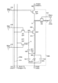
図4に示すように、サブ画素120Aは、第1の発光素子駆動部108A及び第2の発光素子駆動部108Bを有する。第2の発光素子駆動部108Bの構成は、第1の発光素子駆動部108Aの構成と比較して、発光素子が第2の発光素子RLED2であり、保持容量素子が保持容量素子SC2であり、及び駆動電源線が第2の駆動電源線PVDD2である。第2の発光素子駆動部108Bにおいて、発光素子及び駆動電源以外の構成は、第1の発光素子駆動部108Aと同様の構成である。また、サブ画素120B及びサブ画素120Cのそれぞれの構成は、サブ画素120Aと比較して、発光素子が異なる。サブ画素120B及びサブ画素120Cのそれぞれにおいて、発光素子以外の構成は、サブ画素120Aと同様の構成である。よって、以下においては、主に、サブ画素120Aの構成及び第1の発光素子駆動部108Aの構成を説明する。
As shown in FIG. 4, the
図4に示すように、第1の発光素子駆動部108Aは、駆動トランジスタDRT、選択トランジスタSST(第1スイッチ)、初期化トランジスタIST(第2スイッチ)、リセットトランジスタRST(第3スイッチ)、発光制御トランジスタBCT(第4スイッチ)、保持容量素子(容量素子)SC1、第1の発光素子RLED1、カソード容量Ccd及び付加容量Celを含む。これらのトランジスタのそれぞれは、第1電極(ゲート電極)と、第2電極及び第3電極からなる一対の電極(ソース電極、ドレイン電極)を有する。保持容量素子SC1、カソード容量Ccd及び付加容量Celのそれぞれは、一対の電極を有する。なお、付加容量Celは、第1の発光素子RLED1の寄生容量であってよく、第1の発光素子RLED1と並列に設けられた容量素子と第1の発光素子RLED1の寄生容量とを含んでもよい。
As shown in FIG. 4, the first light-emitting
第1の発光素子駆動部108Aの第1の発光素子RLED1を駆動する電源として、第1の駆動電源線PVDD1から第1の駆動電圧VDDH1が供給され、基準電位線PVSSから基準電圧VSSが供給され、リセット信号VL1から電圧Vrstが供給される。また、第2の発光素子駆動部108Bの第2の発光素子RLED2を駆動する電源として、第2の駆動電源線PVDD2から電源VDDH2が供給される。電圧Vrstは、第1の駆動電圧VDDH1、及び第2の駆動電圧VDDH2よりも小さく、基準電位VSSと略同じとすることができる。第1の駆動電圧VDDH1は第2の駆動電圧VDDH2より大きくてもよく、第3の駆動電圧VDDH3は第4の駆動電圧VDDH4より大きくてもよく、第5の駆動電源線PVDD5は第6の駆動電圧VDDH6より大きくてもよい。
As a power source for driving the first light-emitting element RLED1 of the first light-emitting
駆動トランジスタDRTは、入力された映像信号を用いて、第1の発光素子RLED1に電流を流し、第1の発光素子RLED1を発光させる役割を有する。選択トランジスタSSTは、駆動トランジスタDRTに映像信号を供給する役割を有する。初期化トランジスタISTは、駆動トランジスタDRTの第1の電極(ゲート電極)620などに電圧Viniを供給し、駆動トランジスタDRTをリセットする役割を有する。発光制御トランジスタBCTは、第1の駆動電源線PVDD1又は第2の駆動電源線PVD2と駆動トランジスタDRTとの接続、非接続を制御する。発光制御トランジスタBCTは、駆動トランジスタDRTと第1の発光素子RLED1、及び駆動トランジスタDRTと付加容量Celとの電気的な接続、非接続を制御するといってもよい。即ち、発光制御トランジスタBCTは、第1の発光素子RLED1の発光、非発光を制御する役割を有する。また、第2の発光素子駆動部108Bの第2の発光素子RLED2を駆動する電源として、第2の駆動電源線PVDD2から電源VDDH2が供給される。即ち、発光制御トランジスタBCTは、第1の発光素子RLED1の発光、非発光を制御する役割を有する。
The driving transistor DRT uses the input video signal to pass a current through the first light-emitting element RLED1, causing the first light-emitting element RLED1 to emit light. The selection transistor SST has a role of supplying a video signal to the driving transistor DRT. The initialization transistor IST has a role of supplying a voltage Vini to the first electrode (gate electrode) 620 of the driving transistor DRT, etc., and resetting the driving transistor DRT. The light-emitting control transistor BCT controls the connection/disconnection between the first driving power line PVDD1 or the second driving power line PVD2 and the driving transistor DRT. It can be said that the light-emitting control transistor BCT controls the electrical connection/disconnection between the driving transistor DRT and the first light-emitting element RLED1, and between the driving transistor DRT and the additional capacitance Cel. In other words, the light-emitting control transistor BCT has a role of controlling the emission/non-emission of the first light-emitting element RLED1. In addition, a power supply VDDH2 is supplied from the second drive power supply line PVDD2 as a power supply for driving the second light emitting element RLED2 of the second light emitting
リセットトランジスタRSTは、駆動トランジスタDRTの第3の電極630(ドレイン電極630)に電圧Vrstを供給し、第1の発光素子RLED1の第1の電極660に電圧Vrstを供給し、駆動トランジスタDRTの第2の電極610(ソース電極610)、及び第1の発光素子RLED1をリセットする役割を有する。第1の発光素子RLED1の第1の電極660は、例えば、アノード電極である。また、第2の発光素子駆動部108BのリセットトランジスタRSTは、第2の発光素子RLED2の第1の電極660に電圧Vrstを供給し、第1の発光素子駆動部108AのリセットトランジスタRSTと同様の役割を有する。
The reset transistor RST has the role of supplying a voltage Vrst to the third electrode 630 (drain electrode 630) of the drive transistor DRT, supplying a voltage Vrst to the
保持容量素子SC1は、駆動トランジスタDRTの閾値に相当する電圧を確保する役割を有する。また、保持容量素子SC1は、画素120が発光するために駆動トランジスタDRTの第1の電極620(ゲート電極620)に入力する電圧を維持する役割を有する。即ち、保持容量素子SC1は、入力された映像信号を保持するための役割を有する。また、保持容量素子SC2は、保持容量素子SC1と同様の構成を有し、同様の機能を有する。
The capacitance element SC1 has the role of securing a voltage equivalent to the threshold value of the driving transistor DRT. The capacitance element SC1 also has the role of maintaining the voltage input to the first electrode 620 (gate electrode 620) of the driving transistor DRT in order for the
本発明の一実施形態に係る表示装置100は、入力された映像信号を保持するものとして、保持容量素子SC2、保持容量素子SC1などの保持容量素子を有するが、入力された映像信号を保持するものは保持容量素子でなくてもよい。例えば、信号又は電圧を保持可能な素子は、SRAMのように2値のデータを保持可能な素子であってもよい。
The
第1の発光素子RLED1は、ダイオード特性を有する。付加容量Celは、第1の発光素子RLED1が含む容量である。カソード容量Ccdは、第1の発光素子RLED1の第1の電極660と基準電位線PVSSの間に形成される容量である。また、第2の発光素子RLED2は、第1の発光素子RLED1と同様に、ダイオード特性を有する。付加容量Celは、第2の発光素子RLED2が含む容量でもある。カソード容量Ccdは、第2の発光素子RLED2の第1の電極660と基準電位線PVSSの間に形成される容量でもある。なお、本発明の一実施形態においては、付加容量Celと保持容量素子SC1又はSC2とによって、入力された映像信号を保持してもよい。
The first light-emitting element RLED1 has diode characteristics. The additional capacitance Cel is a capacitance included in the first light-emitting element RLED1. The cathode capacitance Ccd is a capacitance formed between the
初期化トランジスタISTのゲート電極は、初期化制御線416に電気的に接続される。初期化制御線416には、初期化制御信号IG(n)が供給される。初期化トランジスタISTは、初期化制御信号IG(n)に供給される信号によって、導通状態、非導通状態が制御される。初期化制御信号IG(n)に供給される信号がローレベル(Low Level、Lレベル)のとき、初期化トランジスタISTは、非導通状態となる。初期化制御信号IG(n)に供給される信号がハイレベル(High Level、Hレベル)のとき、初期化トランジスタISTは、導通状態となる。初期化トランジスタISTのソース電極は、第2リセット電圧線414に電気的に接続される。第2リセット電圧線414には、第2リセット信号VL2が供給される。初期化トランジスタISTのドレイン電極は、駆動トランジスタDRTのゲート電極620、選択トランジスタSSTのドレイン電極、及び保持容量素子SC1の第1の電極640に電気的に接続される。保持容量素子SC1の第2の電極は、駆動トランジスタDRTのソース電極610、リセットトランジスタRSTのドレイン電極、第1の発光素子RLED1の第1の電極660、及び付加容量Celの第1の電極に電気的に接続される。保持容量素子SC2の第2の電極は、第2の発光素子駆動部108Bの駆動トランジスタDRTのソース電極610、第2の発光素子駆動部108BのリセットトランジスタRSTのドレイン電極、第2の発光素子RLED2の第1の電極660、及び付加容量Celの第1の電極に電気的に接続される。
The gate electrode of the initialization transistor IST is electrically connected to the
選択トランジスタSSTのゲート電極は、走査信号線408に電気的に接続される。走査信号線408には、走査信号SG(n)が供給される。選択トランジスタSSTは、走査信号SG(n)に供給される信号によって、導通状態、非導通状態が制御される。走査信号SG(n)に供給される信号がLレベルのとき、選択トランジスタSSTは、非導通状態となる。走査信号SG(n)に供給される信号がHレベルのとき、選択トランジスタSSTは、導通状態となる。選択トランジスタSSTのソース電極は、映像信号線409に電気的に接続される。映像信号線409には、映像信号SL(m)が供給される。
The gate electrode of the selection transistor SST is electrically connected to a
発光制御トランジスタBCTのゲート電極は、発光制御線418に電気的に接続される。発光制御線418には、発光制御信号BG(n)が供給される。発光制御トランジスタBCTは、発光制御信号BG(n)に供給される信号によって、導通状態、非導通状態が制御される。発光制御信号BG(n)に供給される信号がLレベルのとき、発光制御トランジスタBCTは、非導通状態となる。発光制御信号BG(n)に供給される信号がHレベルのとき、発光制御トランジスタBCTは、導通状態となる。発光制御トランジスタBCTのドレイン電極は、第1の駆動電源線PVDD1又は第2の駆動電源線PVDD2に電気的に接続される。第1の駆動電源線PVDD1は、第1の駆動電源線428である。第2の駆動電源線PVDD2は、第2の駆動電源線429である。発光制御トランジスタBCTのソース電極は、駆動トランジスタDRTのドレイン電極630と電気的に接続される。
The gate electrode of the light emission control transistor BCT is electrically connected to the light
リセットトランジスタRSTのゲート電極は、第1リセット信号線412に電気的に接続される。第1リセット信号線412には、第1リセット信号VLが供給される。リセットトランジスタRSTは、第1リセット信号線412に供給される信号によって、導通状態、非導通状態が制御される。第1リセット信号線412に供給される信号がLレベルのとき、リセットトランジスタRSTは、非導通状態となる。第1リセット信号線412に供給される信号がHレベルのとき、リセットトランジスタRSTは、導通状態となる。リセットトランジスタRSTのソース電極は、第1リセット信号VL1が供給される。
The gate electrode of the reset transistor RST is electrically connected to a first
第1の発光素子RLED1の第2の電極670、カソード容量Ccd及び付加容量Celの第2の電極は、基準電圧線PVSSに電気的に接続される。基準電圧線PVSSは、例えば、カソード電極に電気的に接続される。なお、第2の発光素子RLED2の第2の電極670は、第1の発光素子RLED1の第2の電極670と同様に、カソード容量Ccd及び付加容量Celの第2の電極は、基準電圧線PVSSに電気的に接続される。
The
初期化トランジスタISTのドレイン電極、選択トランジスタSSTのドレイン電極、駆動トランジスタDRTのゲート電極620、及び保持容量素子SC1の第1の電極は、第1ノードAに電気的に接続される。リセットトランジスタRSTのドレイン電極、駆動トランジスタDRTのソース電極610、保持容量素子Csの第2の電極、第1の発光素子RLED1の第1の電極660、及び付加容量Celの第1の電極は、第2ノードBに電気的に接続される。駆動トランジスタDRTのドレイン電極630、及び発光制御トランジスタBCTのソース電極は、第3ノードCに電気的に接続される。
The drain electrode of the initialization transistor IST, the drain electrode of the selection transistor SST, the
第1リセット信号線412は、各画素に共通の電圧Vrstを供給するため、本明細書等では第2共通電極と呼ぶ場合がある。第2リセット電圧線414は、各画素に共通の電圧Viniを供給するため、本明細書等では第3共通電極と呼ぶ場合がある。なお、電圧Vrstと電圧Viniは略同一の電圧である。電圧Vrstと電圧Viniが略同一であることによって、駆動トランジスタDRTのリセット時に、駆動トランジスタDRTのゲート電極620の電圧と駆動トランジスタDRTのソース電極610の電圧とを略同一にすることができるため、駆動トランジスタDRTのリセットと、駆動トランジスタDRTの閾値補正との両方を精度よく行うことができる。
The first
本明細書等において、導通状態とは、トランジスタのソース電極とドレイン電極とが導通し、トランジスタがオン(ON)の状態を示すものとする。また、本明細書等において、非導通状態とは、トランジスタのソース電極とドレイン電極とが非導通となり、トランジスタがオフ(OFF)の状態を示すものとする。なお、各トランジスタにおいて、ソース電極とドレイン電極とは、各電極の電圧によって、入れ替わる場合がある。また、トランジスタがオフの状態であっても、リーク電流などのように、わずかに電流が流れることは、当業者であれば容易に理解できることである。 In this specification, the conductive state refers to a state in which the source electrode and drain electrode of a transistor are conductive and the transistor is on (ON). Also, in this specification, the non-conductive state refers to a state in which the source electrode and drain electrode of a transistor are non-conductive and the transistor is off (OFF). Note that in each transistor, the source electrode and drain electrode may be switched depending on the voltage of each electrode. Also, it is easily understood by those skilled in the art that even when a transistor is off, a small amount of current flows, such as a leakage current.
図4に示す各トランジスタは、チャネル領域にシリコンやゲルマニウムなどの14族元素、或いは半導体特性を示す酸化物を有することができる。例えば、各トランジスタのチャネル領域は、低温ポリシリコン(LTPS)を有する。本発明の一実施に係る表示装置100では、各トランジスタは、薄膜トランジスタ(TFT)を用いて形成され、nチャネル型の電界効果トランジスタを有する。各トランジスタはnチャネル型の電界効果トランジスタとpチャネル型の電界効果トランジスタとを有してもよく、pチャネル型の電界効果トランジスタのみを有してもよい。表示装置100は、用途や仕様に応じて、適宜、トランジスタの構成、保持容量の接続、電源電圧などを適合させるとよい。
Each transistor shown in FIG. 4 may have a group 14 element such as silicon or germanium, or an oxide exhibiting semiconductor properties, in the channel region. For example, the channel region of each transistor has low-temperature polysilicon (LTPS). In the
一部のトランジスタは隣接する複数の画素間で共有されてもよい。例えば、リセットトランジスタRSTは、各行に1つ、走査信号線駆動回路510内に設けてもよく、複数の行に1つ、走査信号線駆動回路510内に設けてもよく、各行に1つ、周辺領域516に設けてもよく、複数の行に1つ、周辺領域516に設けてもよい。
Some of the transistors may be shared between adjacent pixels. For example, the reset transistor RST may be provided in the scanning signal
サブ画素120Bは、上記で説明したサブ画素120Aの第1の発光素子RLED1、第2の発光素子RLED2、第1の駆動電源線PVDD1、第2の駆動電源線PVDD2、第1の駆動電圧VDDH1、及び第2の駆動電圧VDDH2のそれぞれを、第1の発光素子GLED1、第2の発光素子GLED2、第3の駆動電源線PVDD3、第4の駆動電源線PVDD4、第3の駆動電圧VDDH3及び第4の駆動電圧VDDH4に置き換えた構成である。その他の構成はサブ画素120Aの構成と同様であるから、ここでの説明は省略する。
また、サブ画素120Cについても、サブ画素120Bと同様に、上記で説明したサブ画素120Aの第1の発光素子RLED1、第2の発光素子RLED2、第1の駆動電源線PVDD1、第2の駆動電源線PVDD2、第1の駆動電圧VDDH1、及び第2の駆動電圧VDDH2のそれぞれを、第1の発光素子BLED1、第2の発光素子BLED2、第5の駆動電源線PVDD5、第6の駆動電源線PVDD6、第5の駆動電圧VDDH5及び第6の駆動電圧VDDH6に置き換えた構成である。その他の構成はサブ画素120Aの構成と同様であるから、ここでの説明は省略する。
Also, in the
画素120の配列は、ストライプ配列である例を示す。また、サブ画素120A、サブ画素120B、及びサブ画素120Cもストライプ状に配列する例を示す。画素120は、表示部504で再現される映像の一部を構成する最小単位である。なお、画素120の配列には制限がなく、例えば、表示装置100の用途又は仕様に基づき適宜決めればよい。例えば、画素120の配列は、デルタ配列、ペンタイル配列などを採用してもよい。
In this example, the
<3.発光素子の面積に対する量子効率と電流密度の関係の一例>
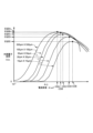
図5は、本発明の一実施形態に係る発光素子の面積に対する量子効率と電流密度の関係を示す模式的な図である。図6は、本発明の一実施形態に係る発光素子の面積に対する量子効率と電流密度の関係を示す模式的な図である。図5及び図6は一例であって、図3及び図4に示すグラフに限定されない。図1~図4と同一、又は類似する構成については、ここでの説明を省略する。
3. An example of the relationship between quantum efficiency and current density relative to the area of the light-emitting element
Fig. 5 is a schematic diagram showing the relationship between the quantum efficiency and the current density with respect to the area of a light-emitting device according to one embodiment of the present invention. Fig. 6 is a schematic diagram showing the relationship between the quantum efficiency and the current density with respect to the area of a light-emitting device according to one embodiment of the present invention. Figs. 5 and 6 are merely examples, and are not limited to the graphs shown in Figs. 3 and 4. Descriptions of configurations that are the same as or similar to those in Figs. 1 to 4 will be omitted here.
図5に示すように、発光素子は、電流密度(mA/μm2)に対して最適な量子効率(%)を有する。量子効率は外部量子効率と呼ばれることもある。最適な量子効率は、発光素子の面積に応じて異なる。例えば、発光素子のチップ面積が500μm×500μmでは、最適な量子効率は、電流密度CDAのときの量子効率EQEAである。発光素子のチップ面積が100μm×100μmでは、最適な量子効率は、電流密度CDBのときの量子効率EQEBである。発光素子の面積が50μm×50μmでは、最適な量子効率は、電流密度CDCのときの量子効率EQECである。発光素子の面積が20μm×20μmでは、最適な量子効率は、電流密度CDDのときの量子効率EQEDである。発光素子の面積が10μm×10μmでは、最適な量子効率は、電流密度CDEのときの量子効率EQEEである。 As shown in FIG. 5, the light-emitting element has an optimal quantum efficiency (%) with respect to the current density (mA/μm 2 ). The quantum efficiency is sometimes called external quantum efficiency. The optimal quantum efficiency varies depending on the area of the light-emitting element. For example, when the chip area of the light-emitting element is 500 μm×500 μm, the optimal quantum efficiency is the quantum efficiency EQEA at the current density CDA. When the chip area of the light-emitting element is 100 μm×100 μm, the optimal quantum efficiency is the quantum efficiency EQEB at the current density CDB. When the area of the light-emitting element is 50 μm×50 μm, the optimal quantum efficiency is the quantum efficiency EQEC at the current density CDC. When the area of the light-emitting element is 20 μm×20 μm, the optimal quantum efficiency is the quantum efficiency EQED at the current density CDD. When the area of the light-emitting element is 10 μm×10 μm, the optimal quantum efficiency is the quantum efficiency EQEE at the current density CDE.
例えば、図6は、第1の発光素子RLED1及び第2の発光素子RLED2に対する量子効率(%)と電流密度(mA/μm2)の関係を示す。例えば、第1の発光素子RLED1のチップ面積が100μm×100μmであり、第2の発光素子RLED2のチップ面積が50μm×50μmである。第2の発光素子RLED2のチップ面積は、第1の発光素子RLED1のチップ面積よりも小さく、第1の発光素子RLED1のチップ面積は第2の発光素子RLED2のチップ面積の2倍又はおよそ2倍である。第1の発光素子RLED1のチップ面積は第2の発光素子RLED2のチップ面積の2 n 倍であってよい。 6 shows the relationship between quantum efficiency (%) and current density (mA/μm2) for the first light-emitting element RLED1 and the second light-emitting element RLED2. For example, the chip area of the first light-emitting element RLED1 is 100 μm×100 μm, and the chip area of the second light-emitting element RLED2 is 50 μm×50 μm. The chip area of the second light-emitting element RLED2 is smaller than the chip area of the first light-emitting element RLED1, and the chip area of the first light-emitting element RLED1 is twice or approximately twice the chip area of the second light-emitting element RLED2. The chip area of the first light-emitting element RLED1 may be 2 n times the chip area of the second light-emitting element RLED2.
また、図6に示すように、第1の発光素子RLED1の最適な量子効率は、電流密度CDFのときの量子効率EQEFである。第2の発光素子RLED2の最適な量子効率は、電流密度CDGのときの量子効率EQEGである。図6に示すように、第1の発光素子RLED1の最適な量子効率は、量子効率の最大値である。 Also, as shown in FIG. 6, the optimal quantum efficiency of the first light-emitting element RLED1 is the quantum efficiency EQEF at the current density CDF. The optimal quantum efficiency of the second light-emitting element RLED2 is the quantum efficiency EQEG at the current density CDG. As shown in FIG. 6, the optimal quantum efficiency of the first light-emitting element RLED1 is the maximum value of the quantum efficiency.
第1の発光素子RLED1の光度L1(第1の光度(cd))は、第1の発光素子RLED1のチップ面積S1及び輝度EQEL1を用いて、式(1)に基づき算出される。第1の発光素子RLED1のチップ面積S1はチップ面積a×bである。第1の発光素子RLED1の光度L1は、L1=a×b×EQEL1である。第2の発光素子RLED2の光度L2(第2の輝度(cd))は、第2の発光素子RLED2のチップ面積S2及び輝度EQEL2を用いて、式(2)に基づき算出される。第2の発光素子RLED2のチップ面積S2はチップ面積c×dである。第2の発光素子RLED2の光度L2は、L2=c×d×EQEL2である。輝度EQEL1は、第1の発光素子RLED1を、最適な量子効率EQEFの電流密度CDFで発光させたときの輝度(cd/m2)である。輝度EQEL2は、第2の発光素子RLED2を、最適な量子効率EQEGの電流密度CDGで発光させたときの輝度(cd/m2)である。即ちこの値は、各発光素子を流れる電流の電流密度と相関がある。 The luminance L1 (first luminance (cd)) of the first light-emitting element RLED1 is calculated based on formula (1) using the chip area S1 and luminance EQEL1 of the first light-emitting element RLED1. The chip area S1 of the first light-emitting element RLED1 is the chip area a×b. The luminance L1 of the first light-emitting element RLED1 is L1=a×b×EQEL1. The luminance L2 (second luminance (cd)) of the second light-emitting element RLED2 is calculated based on formula (2) using the chip area S2 and luminance EQEL2 of the second light-emitting element RLED2. The chip area S2 of the second light-emitting element RLED2 is the chip area c×d. The luminance L2 of the second light-emitting element RLED2 is L2=c×d×EQEL2. The luminance EQEL1 is the luminance (cd/m 2 ) when the first light-emitting element RLED1 is caused to emit light at a current density CDF with the optimal quantum efficiency EQEF. The luminance EQEL2 is the luminance (cd/m 2 ) when the second light-emitting element RLED2 is caused to emit light at a current density CDG with the optimal quantum efficiency EQEG. That is, this value is correlated with the current density of the current flowing through each light-emitting element.
![]()
![]()
![]()
![]()
各発光素子の面積は、式(3)に基づき決定する。式(3)によれば、各発光素子のそれぞれの輝度が等しい場合の互いの面積比は、1:2 n となる。ここで、上述したように、数値nは1以上の任意の整数である。例えば、サブ画素が、3つの発光素子を有する場合、それぞれの発光素子のチップ面積の比が20:21:22=1:2:4で構成される。 The area of each light-emitting element is determined based on formula (3). According to formula (3), when the luminance of each light-emitting element is equal, the area ratio between the light-emitting elements is 1 :2n . Here, as described above, the number n is an arbitrary integer equal to or greater than 1. For example, when a subpixel has three light-emitting elements, the chip area ratio of each light-emitting element is 20 :21: 22 =1:2:4.

発光素子においては、発光素子が発光する輝度は、例えば、発光素子に印加する電圧に対して単調に増加し、発光素子が発光する輝度に対して発光素子に印加する電圧は一意に決定することができる。本発明の一実施形態に係る表示装置100では、第1の駆動電圧VDDH1が第1の発光素子RLED1の光度L1に基づき決定され、第2の駆動電圧VDDH2が第2の発光素子RLED2の光度L2に基づき決定される。
In a light-emitting element, the luminance emitted by the light-emitting element increases monotonically with respect to the voltage applied to the light-emitting element, for example, and the voltage applied to the light-emitting element can be uniquely determined with respect to the luminance emitted by the light-emitting element. In a
また、第1の発光素子RLED1及び第2の発光素子RLED2と同様に、第1の発光素子GLED1及び第2の発光素子GLED2のそれぞれにおいても、第1の発光素子GLED1及び第2の発光素子GLED2の面積に対する量子効率と電流密度の関係と式(1)及び式(2)に基づき、第1の発光素子GLED1の第1の光度L1及び第2の発光素子GLED2の第2の光度L2を算出される。さらに、第3の駆動電圧VDDH3が第1の発光素子GLED1の光度L1に基づき決定され、第4の駆動電圧VDDH4が第2の発光素子GLED2の光度L2に基づき決定される。 Furthermore, similarly to the first light-emitting element RLED1 and the second light-emitting element RLED2, for each of the first light-emitting element GLED1 and the second light-emitting element GLED2, the first luminous intensity L1 of the first light-emitting element GLED1 and the second luminous intensity L2 of the second light-emitting element GLED2 are calculated based on the relationship between the quantum efficiency and the current density relative to the area of the first light-emitting element GLED1 and the second light-emitting element GLED2 and on equations (1) and (2). Furthermore, the third driving voltage VDDH3 is determined based on the luminous intensity L1 of the first light-emitting element GLED1, and the fourth driving voltage VDDH4 is determined based on the luminous intensity L2 of the second light-emitting element GLED2.
また、第1の発光素子RLED1及び第2の発光素子RLED2と同様に、第1の発光素子BLED1及び第2の発光素子BLED2のそれぞれにおいても、第1の発光素子BLED1及び第2の発光素子BLED2の面積に対する量子効率と電流密度の関係と式(1)及び式(2)に基づき、第1の発光素子BLED1の第1の光度L1及び第2の発光素子BLED2の第2の光度L2を算出される。さらに、第5の駆動電圧VDDH5が第1の発光素子BLED1の光度L1に基づき決定され、第6の駆動電圧VDDH6が第2の発光素子BLED2の光度L2に基づき決定される。 Furthermore, similarly to the first light-emitting element RLED1 and the second light-emitting element RLED2, for each of the first light-emitting element BLED1 and the second light-emitting element BLED2, the first luminous intensity L1 of the first light-emitting element BLED1 and the second luminous intensity L2 of the second light-emitting element BLED2 are calculated based on the relationship between the quantum efficiency and the current density relative to the area of the first light-emitting element BLED1 and the second light-emitting element BLED2 and on equations (1) and (2). Furthermore, the fifth driving voltage VDDH5 is determined based on the luminous intensity L1 of the first light-emitting element BLED1, and the sixth driving voltage VDDH6 is determined based on the luminous intensity L2 of the second light-emitting element BLED2.
以上説明したように、発光素子がマイクロLEDの場合、電流密度の最適値はマイクロLEDのチップ面積に依存する。すなわち、発光素子がマイクロLEDの場合、輝度がマイクロLEDのチップ面積に依存するが、チップ面積に必ずしも比例しない。その結果、輝度に応じて、マイクロLEDのチップ面積を最適化することができる。ここで、輝度は、量子効率と関係がある。図5及び図6において、外部量子効率を輝度に置き換えてもよい。すなわち、量子効率の最適値(最大値)はマイクロLEDのチップ面積に依存する。マイクロLEDのチップ面積が小さいほど、最適な電流値は大きく、かつ、最適な量子効率は小さい。マイクロLEDのチップ面積が大きいほど、最適な電流値は小さく、かつ、最適な量子効率は大きい。その結果、量子効率及び電流密度に応じて、マイクロLEDのチップ面積を最適化することができる。 As described above, when the light-emitting element is a micro LED, the optimal value of the current density depends on the chip area of the micro LED. That is, when the light-emitting element is a micro LED, the brightness depends on the chip area of the micro LED, but is not necessarily proportional to the chip area. As a result, the chip area of the micro LED can be optimized according to the brightness. Here, the brightness is related to the quantum efficiency. In Figures 5 and 6, the external quantum efficiency may be replaced with the brightness. That is, the optimal value (maximum value) of the quantum efficiency depends on the chip area of the micro LED. The smaller the chip area of the micro LED, the larger the optimal current value and the smaller the optimal quantum efficiency. The larger the chip area of the micro LED, the smaller the optimal current value and the larger the optimal quantum efficiency. As a result, the chip area of the micro LED can be optimized according to the quantum efficiency and the current density.
また、輝度に応じて、異なる色を発光するマイクロLEDのチップ面積のそれぞれを、発光する色毎に最適化することができる。言い換えると、量子効率及び電流密度に応じて、異なる色を発光するマイクロLEDのチップ面積を、発光する色毎に最適化することができる。 Furthermore, the chip area of each of the micro LEDs that emit different colors can be optimized for each emitted color depending on the luminance. In other words, the chip area of each of the micro LEDs that emit different colors can be optimized for each emitted color depending on the quantum efficiency and current density.
また、本発明の一実施形態に係る表示装置100では、各チップ面積のマイクロLEDに、電流密度に対して量子効率の最大値に基づき算出される各発光素子に固有の輝度に応じた電圧を印加し、各チップ面積のマイクロLEDを発光させることができる。すなわち、複数の面積の異なるマイクロLEDであっても、同一の面積のマイクロLEDは、同一の電流密度に対して最大の量子効率に基づく各マイクロLEDに固有の電圧で駆動することができる。言い換えると、本発明の一実施形態に係る表示装置100では、供給される電圧に合わせて最適な輝度になるように、マイクロLEDのチップ面積を決定することができる。その結果、表示装置100は、色度に差が生じることを軽減でき、かつ、複数のLEDの寿命の差を最小限に抑えることができるため、表示装置の長期信頼性の低下を抑制することができる。
In addition, in the
本発明の一実施形態に係る表示装置100では、異なる色を発光するマイクロLEDのチップ面積に応じて、各マイクロLEDのそれぞれに異なる駆動電圧を供給する構成を有する。具体的には、6個のマイクロLEDチップのそれぞれに対応する第1の駆動電圧VDDH1~第6の駆動電圧VDDH6が6個のマイクロLEDチップに供給される。駆動電圧を供給する構成は、ここで示された構成に限定されない。例えば、駆動電圧は第1の駆動電圧VDDH1及び第2の駆動電圧VDDH2とし、第1の駆動電圧VDDH1は、第1の発光素子RLED1、第1の発光素子GLED1、及び第1の発光素子BLED1に供給され、第2の駆動電圧VDDH2は第2の発光素子RLED2、第2の発光素子GLED2、及び第2の発光素子BLED2に供給されてもよい。このとき、各発光素子のチップ面積は、第1の駆動電圧VDDH1又は第2の駆動電圧VDDH2に対して、量子効率の最大値で発光する輝度になるように構成される。
The
また、各チップ面積のマイクロLEDに、電流密度に対して量子効率の最大値に基づき算出される各発光素子に固有の輝度に応じた電圧を印加し、各チップ面積のマイクロLEDを発光させることができる。すなわち、複数の面積の異なるマイクロLEDであっても、同一の面積のマイクロLEDは、同一の電流密度に対して最大の量子効率に基づく各マイクロLEDに固有の電圧で駆動することができる。言い換えると、本発明の一実施形態に係る表示装置100では、供給される電圧に合わせて最適な輝度になるように、マイクロLEDのチップ面積を決定することができる。その結果、表示装置100は、色度に差が生じることを軽減でき、かつ、複数のLEDの寿命の差を最小限に抑えることができるため、表示装置の長期信頼性の低下を抑制することができる。
In addition, a voltage corresponding to the luminance specific to each light-emitting element calculated based on the maximum quantum efficiency for the current density can be applied to the micro-LEDs of each chip area, causing the micro-LEDs of each chip area to emit light. That is, even if there are multiple micro-LEDs with different areas, micro-LEDs of the same area can be driven with a voltage specific to each micro-LED based on the maximum quantum efficiency for the same current density. In other words, in the
<4.駆動方法>
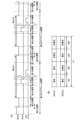
図7は、本発明の一実施形態に係る表示装置100のタイミングチャートを示す模式的な図である。図8~図12は、図7に示すタイミングにおけるサブ画素120Aの第1の発光素子駆動部108Aの動作状態を示す模式的な図である。図13(A)は、本発明の一実施形態に係る表示装置100の第1のサブフレーム期間及び第2のサブフレーム期間の一例を示す図である。図13(B)は、本発明の一実施形態に係る表示装置100の1フレーム(1F)期間の一例を示す図である。図7~図13に示す駆動方法は、本発明の一実施形態に係る表示装置100の駆動方法の一例であって、表示装置100の駆動方法は、図7~図13に示す駆動方法に限定されない。図1~図6と同一、又は類似する構成については、ここでの説明を省略する。
4. Driving method
FIG. 7 is a schematic diagram showing a timing chart of the
各信号線、信号、及び電源線は、例えば、図1~図4を用いて説明したように、映像信号線駆動回路506及び走査信号線駆動回路510から供給される。図7に示すように、区間G(n)、区間G(n+1)、区間G(n+2)及び区間G(n+3)で示される各区間は、n行目の走査信号線からn+3行目の走査信号線の各1水平期間であり、区間G(n)以前、区間G(n+3)以後は省略するが、1行目の走査信号線から最終行の走査信号線まで継続する。図7に示すように、第1の期間、第2の期間、第3の期間、第4の期間、第5の期間、第6の期間、及び第7の期間で示される各期間について、以下詳細に説明する。図7は、一例として、1行目~4行目の各走査信号線408を駆動するためのタイミングチャートを示すが、図8~図13は、n行目m列目のサブ画素120Aの第1の発光素子駆動部108Aの動作状態を示す。
Each signal line, signal, and power line is supplied from the video signal
本明細書等において、発光状態は、単に発光と呼ばれることがあり、発光することと呼ばれることがあり、非発光状態は、単に非発光と呼ばれることがあり、非発光であることと呼ばれることがあり、発光しない状態と呼ばれることがあり、単に発行しないと呼ばれることがある。 In this specification and the like, the light-emitting state may be simply referred to as light-emitting or emitting light, and the non-light-emitting state may be simply referred to as non-light-emitting or being non-light-emitting, or a non-light-emitting state or simply referred to as not emitting light.
また、本発明の一実施形態において、フレーム期間は、2つ以上のサブフレーム期間を含む。ここでは、フレーム期間のうち1つのサブフレーム期間の駆動方法について説明する。 Furthermore, in one embodiment of the present invention, a frame period includes two or more subframe periods. Here, a method for driving one subframe period of a frame period is described.
<4-1.第1の期間(前フレーム発光)>
図7に示す第1の期間において、第1の発光素子駆動部108Aは、あるフレーム期間の処理が開始されるまで、あるフレームの1つ前のフレーム期間の動作状態を維持している。
<4-1. First period (previous frame light emission)>
In a first period shown in FIG. 7, the first light-emitting
発光制御信号BG(n)、及び発光制御信号BG(n+2)にはHレベルが供給され、第1リセット信号RG(n)、初期化制御信号IG(n)、走査信号SG(n)、走査信号SG(n+1)、第1リセット信号RG(n+2)、初期化制御信号IG(n+2)、走査信号SG(n+2)、及び走査信号SG(n+3)には、Lレベルが供給される。なお、以降の説明では、n行目の走査信号線及びn+1行目の走査信号線に着目し、説明する。n+2行目の走査信号線及びn+3行目の走査信号線では、n行目の走査信号線及びn+1行目の走査信号線で実行された処理と同様の処理が第3の期間以降に実行される。 The light emission control signal BG(n) and the light emission control signal BG(n+2) are supplied with an H level, and the first reset signal RG(n), the initialization control signal IG(n), the scanning signal SG(n), the scanning signal SG(n+1), the first reset signal RG(n+2), the initialization control signal IG(n+2), the scanning signal SG(n+2), and the scanning signal SG(n+3) are supplied with an L level. In the following description, attention is focused on the nth row scanning signal line and the n+1th row scanning signal line. In the n+2th row scanning signal line and the n+3th row scanning signal line, the same processing as that performed in the nth row scanning signal line and the n+1th row scanning signal line is performed in the third period and thereafter.
<4-2.第2の期間(駆動トランジスタDRTのソース電極初期化)>
図8は、n行目m列目のサブ画素120Aの第1の発光素子駆動部108Aの図7に示す第2の期間の動作状態を示す。第1リセット信号RG(n)にはHレベルが供給され、発光制御信号BG(n)には、Lレベルが供給される。よって、初期化トランジスタIST、選択トランジスタSST、及び発光制御トランジスタBCTは非導通状態である。一方、リセットトランジスタRSTは導通状態である。なお、駆動トランジスタDRTは、非導通状態であるとするが、導通状態であってもよい。第2の期間では、第1の駆動電源線PVDD1から第1の発光素子RLED1の第1の電極660の方向への電流が発光制御トランジスタBCTによって遮断される。その結果、第1の発光素子RLED1が非発光となると共に、ノードB、ノードCなどに残留していた電荷が駆動トランジスタDRTとリセットトランジスタRSTとを通じて引き抜かれる。その結果、駆動トランジスタDRTのソース電極610が電圧Vrstに固定される。保持容量素子SC1の第1の電極640及びノードAの電圧は、1つ前のフレームで書き込んだ映像信号の電圧である。電圧Vrstは、基準電圧VSSに対して、第1の発光素子RLED1の発光開始電圧よりも低い電圧である。
<4-2. Second period (initialization of source electrode of driving transistor DRT)>
FIG. 8 shows the operation state of the first light-emitting
<4-3.第3の期間(駆動トランジスタDRTのゲート電極初期化)>
図9は、n行目m列目のサブ画素120Aの第1の発光素子駆動部108Aの図7に示す第3の期間の動作状態を示す。初期化制御信号IG(n)に供給される電圧がLレベルからHレベルになることに伴い、初期化トランジスタISTが導通状態となる。第3の期間では、初期化トランジスタISTを介して駆動トランジスタDRTのゲート電極620が電圧Viniに固定される。即ち、駆動トランジスタDRTのソース電極610と駆動トランジスタDRTのゲート電極620とがリセット(初期化)される。電圧Viniは、電圧Vrstに対して駆動トランジスタDRTのしきい値電圧よりも大きい電圧に設定される。即ち、駆動トランジスタDRTは導通状態となる。ただし、発光制御トランジスタBCTが非導通状態であるため、第1の駆動電源線PVDD1から第1の発光素子RLED1の第1の電極660の方向への電流は駆動トランジスタDRTに流れない。ノードAの電圧は電圧Viniである。
<4-3. Third period (initialization of gate electrode of driving transistor DRT)>
FIG. 9 shows the operation state of the first light-emitting
<4-4.第4の期間(オフセットキャンセル動作)>
図10は、n行目m列目のサブ画素120Aの第1の発光素子駆動部108Aの図7に示す第4の期間の動作状態を示す。発光制御信号BG(n)に供給される電圧は、LレベルからHレベルになる。よって、発光制御トランジスタBCTが導通状態となる。また、リセットトランジスタRSTは非導通状態となる。よって、発光制御トランジスタBCTが第1の駆動電源線PVDD1(第1の駆動電源線428)に接続されるため、ノードCの電圧が第1の駆動電源線PVDD1に供給される電圧VDDH1となる。その結果、駆動トランジスタDRTに、第1の駆動電源線PVDD1から第1の発光素子RLED1の第1の電極660の方向への電流が流れる(駆動トランジスタDRTは第2の期間における動作によって導通状態とされている)。したがって、駆動トランジスタDRTのソース電極610及び保持容量素子SC1の第2の電極650が充電される。
<4-4. Fourth period (offset cancel operation)>
FIG. 10 shows the operation state of the first light-emitting
ノードAの電圧は電圧Viniに固定されている。駆動トランジスタDRTのソース電極610の電圧及びノードBの電圧がVini-Vthになると、駆動トランジスタDRTのゲート電極620とソース電極610との間の電圧がVthとなるため、駆動トランジスタDRTは非導通状態となる。表示装置100は、第4の期間において、ノードAとノードBとの間(保持容量素子SC1)に、駆動トランジスタDRTのしきい値電圧に相当する電荷を保持することができ、駆動トランジスタDRTの閾値を補正することができる。このとき、第1の発光素子駆動部108Aの第1の電極660と第2の電極670との間には、{(Vini-Vth)-PVSS}の電圧が供給されているが、この電圧は第1の発光素子RLED1の発光開始電圧を上回っていないため、電流は第1の発光素子RLED1に流れない。なお、ノードCの電圧はVDDH1である。Vthは、駆動トランジスタのしきい値電圧である。
The voltage of node A is fixed to voltage Vini. When the voltage of the
なお、図7のタイミングチャートによると、第1の期間~第4の動作は、2行分の走査信号線の動作を並行して実行しているが、表示装置100の駆動方法は図7のタイミングチャートに限定されない。第1の期間~第4の動作は、1行の走査信号線ごとに順次実施されてもよく、3行以上の走査信号線の動作を並行して実行してもよい。
Note that, according to the timing chart of FIG. 7, the first to fourth operations are performed in parallel for two rows of scanning signal lines, but the driving method of the
<4-5.第5の期間及び第6の期間(映像信号書き込み動作)>
図11は、n行目m列目のサブ画素120Aの第1の発光素子駆動部108Aの図7に示す第5の期間の動作状態を示す。第4の期間と第5の期間との間において、初期化制御信号IG(n)に供給される電圧は、HレベルからLレベルになる。よって、初期化トランジスタISTは非導通状態となる。また、第4の期間と第5の期間との間において、走査信号SG(n)に供給される電圧は、LレベルからHレベルになる。よって、選択トランジスタSSTが導通状態となる。映像信号線409aに映像信号SL(m)の電圧Vsig(n)が供給されると、駆動トランジスタDRTのゲート電極620に電圧Vsig(n)が供給され、駆動トランジスタDRTのゲート電極620の電圧が電圧Vsig(n)となる。一方、駆動トランジスタDRTのソース電極610の電圧は(Vini-Vth)である。その結果、駆動トランジスタDRTのゲート電極620とソース電極610との間の電圧が、{Vsig-(Vini-Vth)}となり、発光素子駆動部それぞれの駆動トランジスタDRTのしきい値のばらつきが反映されたものとなる。
<4-5. Fifth Period and Sixth Period (Video Signal Writing Operation)>
FIG. 11 shows the operation state of the first light-emitting
第6の期間は、n+1行目m列目のサブ画素120Aの第1の発光素子駆動部108Aの動作状態を示す。第6の期間は、第5の期間と比較して、走査信号SG(n+1)が供給される以外は同様であるから、ここでの説明は省略する。
The sixth period indicates the operating state of the first light-emitting
映像信号線409aは、同列に属する複数行の画素で共通であるため、映像信号書込み動作は、走査信号線1行ごとに順次実行される。
Since the
<4-6.第7の期間(発光又は非発光動作)>
図12は、n行目m列目のサブ画素120Aの第1の発光素子駆動部108Aの図7に示す第7の期間の動作状態を示す。第5の期間と第6の期間の間において、走査信号SG(n)に供給される電圧は、HレベルからLレベルになる。よって、選択トランジスタSSTが非導通状態となる。駆動トランジスタDRTは、第5の期間までに設定された駆動トランジスタDRTのゲート電極620とソース電極610との間の電圧(映像信号の電圧)に応じて、第1の駆動電源線PVDD1から第1の発光素子RLED1の第1の電極660の方向に電流を流すことができる。したがって、第1の発光素子RLED1が、駆動トランジスタDRTの流した電流に応じた輝度で発光する。
<4-6. Seventh period (light emitting or non-light emitting operation)>
12 shows the operation state of the first light-emitting
第1の発光素子RLED1の第1の電極660と第2の電極670との間の電圧は、駆動トランジスタDRTの流した電流に応じた電圧となる。駆動トランジスタDRTの流した電流によって第1の電極660の電圧が上昇するため、第1の電極660と保持容量素子SC1とのカップリングによって駆動トランジスタDRTのゲート電極620の電圧も上昇する。駆動トランジスタDRTのゲート電極には、保持容量素子SC1、付加容量Cel、カソード容量Ccd、及びその他の寄生容量が付加付しているため、第1の電極660の電圧の上昇よりも、駆動トランジスタDRTのゲート電極620の電圧の上昇はわずかに小さくなる。具体的には、電圧の上昇分は、Vel×Cs/(Cs+Ccd+Cel)となる。ここで、電圧Velは、第1の発光素子RLED1の第1の電極660と第2の電極670との間の電圧であり、容量値Csは保持容量素子SC1の容量値であり、容量値Celは付加容量Celの容量値であり、容量値Ccdはカソード容量Ccdの容量値である。したがって、電圧の上昇分は既知であるから、第1の発光素子RLED1に流す電流値が、駆動トランジスタDRTのゲート電極620とソース電極610との間の電圧に応じた所望の電流値となるように、電圧Vsig(n)の電圧を決定すればよい。
The voltage between the
例えば、駆動トランジスタDRTのゲート電極620の電圧は、Vsig-(Vini-Vth)+Vel×Cs/(Cs+Ccd+Cel)であり、駆動トランジスタDRTのソース電極610の電圧は電圧Velである。駆動トランジスタDRTのゲート電極620とソース電極610との間の電圧は、Vsig-(Vini-Vth)-Vel×(Ccd+Cel)/(Cs+Ccd+Cel)である。Vsig-(Vini-Vth)-Vel×(Ccd+Cel)/(Cs+Ccd+Cel)がVthより大きく、Velが第1の発光素子RLED1の発光開始電圧より大きい場合、駆動トランジスタDRTは発光素子RLED1に電流を流し、第1の発光素子RLED1は発光する。Vsig-(Vini-Vth)-Vel×(Ccd+Cel)/(Cs+Ccd+Cel)がVthより大きく、Velが第1の発光素子RLED1の発光開始電圧より小さい場合、駆動トランジスタDRTは発光素子RLED1に電流を流すが、第1の発光素子RLED1は非発光である。Vsig-(Vini-Vth)-Vel×(Ccd+Cel)/(Cs+Ccd+Cel)がVthより小さい場合、駆動トランジスタDRTは発光素子RLED1に電流を流さず、第1の発光素子RLED1は非発光である。
For example, the voltage of the
以上説明したように、サブ画素120Aの第1の発光素子駆動部108Aの一連の動作が完了する。第1の発光素子駆動部108Aと同様に、第2の発光素子駆動部108Bの動作も完了する。また、サブ画素120Aと同様に、サブ画素120B及びサブ画素120Cの動作も完了する。当該動作を走査信号線の1行目の各サブ画素から最終行のサブ画素まで完了すると、1つサブフレーム期間(例えば、第1のサブフレーム期間)の動作が完了し、同様の動作を複数のサブフレーム期間(例えば、第2のサブフレーム期間、第3のサブフレーム期間)で繰り返し実行することで、1フレーム期間内での1画面の映像となる。当該動作を繰り返し、表示装置100の表示部504に映像が表示される。
As described above, a series of operations of the first light-emitting
また、本発明の一実施形態に係る表示装置100は、1つのサブフレーム期間内で、サブ画素120Aの第1の発光素子RLED1及び第2の発光素子RLED2のそれぞれの発光又は非発光を制御し、サブ画素120Aが発光する面積を変えることができる。サブ画素120Aと同様に、サブ画素120B及びサブ画素120Cのそれぞれが発光する面積も変えることができる。
In addition, the
よって、本発明の一実施形態に係る表示装置100は、発光素子が発光する面積を制御し、各画素の階調を制御することができる。ここで、本発明の一実施形態に係る表示装置100が有する複数の発光素子の面積は予め決まっているため、発光素子の面積を制御し、各画素の階調を制御することは、デジタル階調制御と呼んでもよい。また、本発明の一実施形態に係る表示装置100が有する複数の発光素子のそれぞれの面積は、量子効率の最適値、又は、輝度に応じて最適化される。また、本発明の一実施形態に係る表示装置100が有する複数の発光素子は、少なくとも2つの異なる面積を有する2つの発光素子を有し、面積が異なっていても、量子効率の最適値に基づき算出された各発光素子に固有の輝度に対応する電圧で発光することができる。その結果、表示装置100は、色度の差が生じにくく、複数の発光素子の寿命の差を抑制することができるため、長期信頼性の低下を軽減することができる。
Therefore, the
<4-7.サブフレーム期間>
図13(A)に示すように、第1のサブフレーム期間では、発光制御信号BG(n)に供給される電圧がHレベルである時間は、時間BGon1である。第2のサブフレーム期間では、発光制御信号BG(n)に供給される電圧がHレベルである時間は、時間BGon2である。時間BGon1は時間BGon2より短い。発光制御信号BG(n)は発光制御トランジスタBCTの導通状態の時間を制御し、第1の発光素子RLED1及び第2の発光素子RLED2に供給する電流量を制御することができる。その結果、本発明の表示装置100は、複数のサブフレーム期間毎に画素(発光素子)の発光又は非発光の時間を変えることができる。
<4-7. Subframe period>
13A, in the first subframe period, the time during which the voltage supplied to the light-emitting control signal BG(n) is at the H level is time BGon1. In the second subframe period, the time during which the voltage supplied to the light-emitting control signal BG(n) is at the H level is time BGon2. Time BGon1 is shorter than time BGon2. The light-emitting control signal BG(n) controls the time during which the light-emitting control transistor BCT is in a conductive state, and can control the amount of current supplied to the first light-emitting element RLED1 and the second light-emitting element RLED2. As a result, the
本発明の一実施形態に係る発光素子は、式(1)及び式(2)に示されるように、最適化された量子効率に基づく一定の光度で発光する。また、本発明の一実施形態に係る表示装置100は、発光素子が一定の光度で発光する時間をサブフレーム毎に積算し、各画素の階調を制御することができる。ここで、本発光する時間を積算し、各画素の階調を制御し、各画素の階調を制御することは、アナログ階調制御と呼んでもよい。
The light-emitting element according to one embodiment of the present invention emits light at a constant luminous intensity based on optimized quantum efficiency, as shown in formulas (1) and (2). Furthermore, the
図13(B)に示すように、1フレーム(1F)期間は、例えば、第1のサブフレーム期間1SF、第2のサブフレーム期間2SF、第3のサブフレーム期間3SF、及び第4のサブフレーム期間4SFを有する。第1のサブフレーム期間1SFにおいて、例えば、第1の発光素子RLED1及び第2の発光素子RLED2はいずれも発光する。第2のサブフレーム期間2SFにおいて、例えば、第1の発光素子RLED1は発光し、第2の発光素子RLED2は非発光である。第3のサブフレーム期間3SFにおいて、例えば、第1の発光素子RLED1は非発光であり、第2の発光素子RLED2は発光する。第4のサブフレーム期間4SFにおいて、例えば、第1の発光素子RLED1及び第2の発光素子RLED2はいずれも非発光である。 As shown in FIG. 13B, one frame (1F) period has, for example, a first subframe period 1SF, a second subframe period 2SF, a third subframe period 3SF, and a fourth subframe period 4SF. In the first subframe period 1SF, for example, the first light-emitting element RLED1 and the second light-emitting element RLED2 both emit light. In the second subframe period 2SF, for example, the first light-emitting element RLED1 emits light and the second light-emitting element RLED2 does not emit light. In the third subframe period 3SF, for example, the first light-emitting element RLED1 does not emit light and the second light-emitting element RLED2 emits light. In the fourth subframe period 4SF, for example, the first light-emitting element RLED1 and the second light-emitting element RLED2 both do not emit light.
本発明の一実施形態に係る表示装置100は、少なくとも異なる面積を有する2つの発光素子を有し、2つの発光素子のそれぞれの発光又は非発光をサブフレーム毎に制御(デジタル階調制御)することができる。
A
また、本発明の一実施形態に係る表示装置100は、図13(A)に示されるアナログ階調制御と、図13(B)に示されるデジタル階調制御を組み合わせて、各発光素子の階調を制御し、各画素の階調を制御することができる。アナログ階調制御とデジタル階調制御を組み合わせることで、表示装置100は、さらに高階調な映像を表示部504に表示することができる。さらに、本発明の一実施形態に係る表示装置100は、各発光素子の面積を単に2の階乗にするだけでなく、発光素子の面積及び発光素子の発光色に応じて、発光素子毎に異なる量子効率の最適値に基づき輝度が設定される。その結果、表示装置100は、さらに鮮明な映像を表示部504に表示することができる。
In addition, the
なお、本発明の一実施形態に係る表示装置100において、第1の駆動電圧VDDH1、第2の駆動電圧VDDH2、第3の駆動電圧VDDH3、第4の駆動電圧VDDH4、第5の駆動電圧VDDH5及び第6の駆動電圧VDDH6は、例えば、外部回路から端子電極514を経由し、映像信号線駆動回路506、走査信号線駆動回路510から、各画素(サブ画素)に供給する。駆動電圧を各画素(サブ画素)に供給する構成は、ここで示される構成に限定されない。上記で説明したように、駆動電圧は式(1)、式(2)又は式(3)に基づく輝度によって決定されるが、式(1)、式(2)又は式(3)に基づく輝度のデータと、それぞれの輝度に対する駆動電圧のデータを、例えば、ルックアップテーブルなどの記憶装置に記憶してもよい。本発明の一実施形態に係る表示装置100は、当該記憶装置を有し、記憶装置から駆動電圧及び輝度のデータを読み出し、読み出した駆動電圧及び輝度に応じて電圧発生回路などを用いて駆動電圧を生成してもよい。
In the
<5.表示装置100の断面の一例>
図14は、本発明の一実施形態に係る表示装置100の断面の一例を示す断面図である。具体的には、図14は、図3に示すサブ画素120AのA1とA2の断面に沿った断面図である。図14に示す断面は、本発明の一実施形態に係る表示装置100の断面の一例であって、表示装置100の断面は、図14に示すに限定されない。図1~図13と同一、又は類似する構成については、ここでの説明を省略する。
5. Example of Cross Section of
Fig. 14 is a cross-sectional view showing an example of a cross section of the
表示装置100において、半導体層70A、70B、70C及び70Dが、基板502の上面に、任意の構成である下地膜501を介して、設けられる。
In the
第1の発光素子駆動部108Aの駆動トランジスタDRT及び選択トランジスタSST、第2の発光素子駆動部108Bの駆動トランジスタDRT及び選択トランジスタSSTが、下地膜501の上側に設けられる。第1の発光素子駆動部108Aの駆動トランジスタDRTは、半導体層70A、ゲート絶縁膜50、ゲート電極72A(620)、ソース電極84A(610)、ドレイン電極86A(630)を含む。第1の発光素子駆動部108Aの駆動トランジスタSSTは、半導体層70B、ゲート絶縁膜50、ゲート電極72B(410)、ソース電極84B(ノードA)、ドレイン電極86B(630)を含む。
The driving transistor DRT and selection transistor SST of the first light-emitting
第2の発光素子駆動部108Bの駆動トランジスタDRTは、半導体層70B、ゲート絶縁膜50、ゲート電極72C(410)、ソース電極84C(610)、ドレイン電極86C(630)を含む。第2の発光素子駆動部108Bの駆動トランジスタSSTは、半導体層70D、ゲート絶縁膜50、ゲート電極72D(410)、ソース電極84D(ノードA)、ドレイン電極86D(630)を含む。ソース電極又はドレイン電極は、半導体層70A、70B、70C及び70Dに不純物を注入することで形成されてもよい。
The driving transistor DRT of the second light-emitting
ゲート電極72A、72B、72C及び72Dのそれぞれは、ゲート絶縁膜50を間に挟んで、半導体層70A、70B、70C及び70Dと重畳する。半導体層がゲート電極に重なる領域が各トランジスタのチャネル領域である。各半導体層はチャネル領域を挟むようにソース及びドレイン領域を有してもよい。絶縁膜90がゲート電極上に設けられる。
Each of the
ソース電極84A(610)、ドレイン電極86A(630)、ソース電極84B(ノードA)、ドレイン電極86B(630)、ソース電極84C(610)、ドレイン電極86C(630)、ソース電極84D(ノードA)、及びドレイン電極86D(630)のそれぞれは、絶縁膜90又はゲート絶縁膜の一部を露出した開口部74A,76A,74B、76B、74C、76C、74D、及び76Dを介して、半導体層70A、70B、70C及び70Dのそれぞれと電気的に接続される。例えば、コンタクトホール208も、絶縁膜90又はゲート絶縁膜の一部を露出した開口部のうちの一つである。
The
第1平坦化層104は、第1導電層102上に設けられる。第1平坦化層104は、第1導電層102の一部を露出する開口部122を有する。第2導電層106、第1絶縁層109、及び第3導電層110は、この順に、第1平坦化層104上に設けられる。第1絶縁層109は、第1導電層102の一部を露出する開口部122を有する。第3導電層110は、開口部122を介して、第1導電層102と電気的に接続される。
The
第2平坦化層112は、第3導電層110上に設けられる。第2平坦化層112は、開口部126と、開口部128とを有する。開口部126及び開口部128では、第3導電層110の一部が露出される。第4導電層114及び第5導電層116は、この順に、第2平坦化層112上に設けられる。第4導電層114は、開口部126を介して第3導電層110と電気的に接続される。また、第4導電層114は、開口部128を介して第3導電層110と電気的に接続される。
The
第3平坦化層118は、第1の発光素子RLED1及び第2の発光素子RLED2が第3平坦化層118内に埋設されるように設けられる。なお、図示は省略するが、第1の発光素子GLED1及び第2の発光素子GLED2、第1の発光素子BLED1及び第2の発光素子BLED2も、第1の発光素子RLED1及び第2の発光素子RLED2と同様に、第3平坦化層118内に埋設されるように設けられる。第3平坦化層118は、第5導電層116の一部が露出された開口部130を有する。第6導電層150は、第3平坦化層118上に設けられ、開口部140を介して第5導電層116と電気的に接続される。
The
絶縁膜90は各トランジスタ上に設けられる。絶縁膜90はトランジスタやその他の半導体素子に起因する凹凸を吸収し平坦な表面を与える機能を有する。絶縁膜90は、膜表面の平坦性に優れるアクリル、ポリイミド等から選ばれた有機化合物材料を用いることができる。
The insulating
第1導電層102には、ソース電極84A(610)、ドレイン電極86A(630)、ソース電極84B(ノードA)、ドレイン電極86B(630)、ソース電極84C(610)、ドレイン電極86C(630)、ソース電極84D(ノードA)、及びドレイン電極86D(630)、映像信号線409a及び409b、第1の駆動電源線PVDD1及び第2の駆動電源線PVDD2、第1の電極配線210が設けられる。第1導電層102は、絶縁膜90又はゲート絶縁膜の一部を露出した開口部によって、ゲート電極72A(620)、ゲート電極72B(410)、ゲート電極72C(410)、及びゲート電極72D(410)と接続されてもよい。なお、第1の配線206、ゲート電極72A(620)、ゲート電極72B(410)、ゲート電極72C(410)、及びゲート電極72D(410)は、第1導電層102に対してゲート絶縁膜50が設けられる側に設けられる。第1導電層102、第1の配線206及び各ゲート電極の材料として、例えば、アルミニウム(Al)、チタン(Ti)、モリブデン(Mo)、銅(Cu)、またはタングステン(W)などの金属、又はこれらの合金を用いることができる。また、第1導電層102は、単層または積層とすることができる。
The first
第2導電層106には、例えば、保持容量素子SC1の第1の電極640及び保持容量素子SC2の第1の電極640が設けられる。第2導電層106の材料として、例えば、インジウム・スズ酸化物(ITO)またはインジウム・亜鉛酸化物(IZO)などの透明導電材料を用いることができる。
The second
第3導電層110は、第1導電層102と第4導電層114とを接続するための配線層として機能することができる。例えば、第1の発光素子駆動部108Aの保持容量素子SC1の第2の電極650及び第2の発光素子駆動部108Bの保持容量素子SC2の第2の電極650が第3導電層110に設けられる。第3導電層110の材料として、例えば、アルミニウム(Al)、チタン(Ti)、モリブデン(Mo)、銅(Cu)、またはタングステン(W)などの金属、もしくはこれらの合金を用いることができる。また、第1導電層102は、単層または積層とすることができる。
The third
第4導電層114は、第1の発光素子RLED1及び第2の発光素子RLED2、第1の発光素子GLED1及び第2の発光素子GLED2、第1の発光素子BLED1及び第2の発光素子BLED2を実装するための電極パッドとして機能することができる。例えば、第1の発光素子RLED1の第1の電極660及び第2の発光素子RLED2の第1の電極660が第4導電層114に設けられる。また、第4導電層114は、第1の発光素子RLED1及び第2の発光素子RLED2、第1の発光素子GLED1及び第2の発光素子GLED2、第1の発光素子BLED1及び第2の発光素子BLED2から出射された光を反射する反射層として機能することができる。第4導電層114として、例えば、アルミニウム(Al)、チタン(Ti)、モリブデン(Mo)、銅(Cu)、またはタングステン(W)などの金属、もしくはこれらの合金を用いることができる。また、第1導電層102は、単層または積層とすることができる。
The fourth
第5導電層116は、第1の発光素子RLED1及び第2の発光素子RLED2、第1の発光素子GLED1及び第2の発光素子GLED2、第1の発光素子BLED1及び第2の発光素子BLED2を接合するための接合層として機能することができる。第5導電層116として、例えば、銀ペースト、ハンダ、または異方性導電膜(ACF)を用いることができる。
The fifth
第6導電層150は、第1の発光素子RLED1の第1の電極660及び第2の発光素子RLED2の第1の電極660、第1の発光素子GLED1の第1の電極660及び第2の発光素子GLED2の第1の電極660、第1の発光素子BLED1の第1の電極660及び第2の発光素子BLED2の第1の電極660、即ち、カソード電極を引き回すための配線層として機能することができる。即ち、カソード電極に接続される又はカソード電極として機能する基準電圧線PVSSが第6導電層150上に設けられる。また、第6導電層150は、第1の発光素子RLED1及び第2の発光素子RLED2、第1の発光素子GLED1及び第2の発光素子GLED2、第1の発光素子BLED1及び第2の発光素子BLED2から出射された光を透過する透過層として機能することができる。第6導電層150として、例えば、インジウム・スズ酸化物(ITO)またはインジウム・亜鉛酸化物(IZO)などの透明導電材料を用いることができる。
The sixth
第1絶縁層109は、第2導電層106と第3導電層110とを離隔し、絶縁化することができる。第1絶縁層109の材料として、例えば、酸化シリコン(SiOx)、酸化窒化シリコン(SiOxNy)、窒化シリコン(SiNx)、窒化酸化シリコン(SiNxOy)、酸化アルミニウム(AlOx)、酸化窒化アルミニウム(AlOxNy)、窒化酸化アルミニウム(AlNxOy)、または窒化アルミニウム(AlNx)などの無機絶縁材料を用いることができる。ここで、SiOxNyおよびAlOxNyは、酸素(O)よりも少ない量の窒素(N)を含有するシリコン化合物およびアルミニウム化合物である。また、SiNxOyおよびAlNxOyは、窒素よりも少ない量の酸素を含有するシリコン化合物およびアルミニウム化合物である。また、第1絶縁層109は、無機絶縁材料だけでなく、有機絶縁材料を用いることもできる。有機絶縁材料として、例えば、ポリイミド樹脂、アクリル樹脂、エポキシ樹脂、シリコーン樹脂、フッ素樹脂、またはシロキサン樹脂などを用いることができる。第1絶縁層109は、無機絶縁層材料および有機絶縁材料が各々単独で用いられてもよく、これらが積層されてもよい。
The first insulating
第1平坦化層104および第2平坦化層112は、それぞれの下方に位置する層の凹凸を平坦にすることができる。また、第1平坦化層104は、電流供給線244を他の導電層から離隔し、絶縁化することができる。第1平坦化層104および第2平坦化層112の各々の材料として、例えば、ポリイミド樹脂、アクリル樹脂、エポキシ樹脂、シリコーン樹脂、フッ素樹脂、またはシロキサン樹脂などの有機樹脂を用いることができる。第1平坦化層104および第2平坦化層112の各々は、有機樹脂が単独で用いられてもよく、積層されていてもよい。
The
第3平坦化層118は、第6導電層を形成するにあたり、第1の発光素子RLED1及び第2の発光素子RLED2、第1の発光素子GLED1及び第2の発光素子GLED2、第1の発光素子BLED1及び第2の発光素子BLED2との段差を低減し、平坦にすることができる。第3平坦化層118の材料として、例えば、感光性アクリルまたは感光性ポリイミドなどの感光性有機材料を用いることができる。
When forming the sixth conductive layer, the
本発明の一実施形態における表示装置は、上述した積層構造を有することができる。本発明の一実施形態における表示装置は、上述した積層構造を有し、表示装置の長期信頼性の低下を抑制する。 The display device according to one embodiment of the present invention can have the above-mentioned laminated structure. The display device according to one embodiment of the present invention has the above-mentioned laminated structure, which suppresses deterioration of the long-term reliability of the display device.
本発明の実施形態として上述した各実施形態は、相互に矛盾しない限りにおいて、適宜組み合わせて実施することができる。また、各実施形態の表示装置を基にして、当業者が適宜構成要素の追加、削除もしくは設計変更を行ったもの、又は、工程の追加、省略もしくは条件変更を行ったものも、本発明の要旨を備えている限り、本発明の範囲に含まれる。 The above-described embodiments of the present invention may be combined as appropriate to the extent that they are not mutually inconsistent. In addition, a display device according to any of the embodiments may be combined as appropriate by a person skilled in the art to add or remove components or modify the design, or to add or omit processes or modify conditions, and this is also included in the scope of the present invention as long as it contains the gist of the present invention.
上述した各実施形態の態様によりもたらされる作用効果とは異なる他の作用効果であっても、本明細書の記載から明らかなもの、又は、当業者において容易に予測し得るものについては、当然に本発明によりもたらされるものと解される。 Even if there are other effects and advantages different from those brought about by the aspects of each of the above-mentioned embodiments, if they are clear from the description in this specification or can be easily predicted by a person skilled in the art, they are naturally understood to be brought about by the present invention.
50:ゲート絶縁膜、70A:半導体層、70B:半導体層、70C:半導体層、70D:半導体層、72A:ゲート電極、72B:ゲート電極、72C:ゲート電極、72D:ゲート電極、74A:開口部、74B:開口部、74C:開口部、74D:開口部、76A:開口部、76B:開口部、76C:開口部、84A:ソース電極、84B:ソース電極、84C:ソース電極、84D:ソース電極、86A:ドレイン電極、86B:ドレイン電極、86C:ドレイン電極、86D:ドレイン電極、90:絶縁膜、100:表示装置、102:第1導電層、104:第1平坦化層、106:第2導電層、108A:第1の発光素子駆動部、108B:第2の発光素子駆動部、109:第1絶縁層、110:第3導電層、112:第2平坦化層、114:第4導電層、116:第5導電層、118:第3平坦化層、120:画素、120A:サブ画素、120B:サブ画素、120C:サブ画素、122:開口部、126:開口部、128:開口部、130:開口部、140:開口部、150:第6導電層、206:第1の配線、208:コンタクトホール、210:第1の電極配線、212:第1の電極、216:第2の配線、218:コンタクトホール、220:第2の電極配線、222:第2の電極、244:電流供給線、408:走査信号線、409:映像信号線、409a:映像信号線、409b:映像信号線、410:ゲート電極、412:第1リセット信号線、414:第2リセット電圧線、416:初期化制御線、418:発光制御線、428:第1の駆動電源線、429:第2の駆動電源線、501:下地膜、502:基板、504:表示部、506:映像信号線駆動回路、510:走査信号線駆動回路、512:コネクタ、514:端子電極、516:周辺領域、518:制御回路、610:第2の電極、610:ソース電極、620:第1の電極(ゲート電極)、620:第1の電極、620:ゲート電極、630:第3の電極、630:ドレイン電極、640:第1の電極、650:第2の電極、660:第1の電極、670:第2の電極 50: gate insulating film, 70A: semiconductor layer, 70B: semiconductor layer, 70C: semiconductor layer, 70D: semiconductor layer, 72A: gate electrode, 72B: gate electrode, 72C: gate electrode, 72D: gate electrode, 74A: opening, 74B: opening, 74C: opening, 74D: opening, 76A: opening, 76B: opening, 76C: opening, 84A: source electrode, 84B: source electrode, 84C: source electrode, 84D: source electrode, 86A: drain electrode, 86B: drain electrode, 86C: drain electrode, 86D: drain Rain electrode, 90: insulating film, 100: display device, 102: first conductive layer, 104: first planarization layer, 106: second conductive layer, 108A: first light-emitting element driving section, 108B: second light-emitting element driving section, 109: first insulating layer, 110: third conductive layer, 112: second planarization layer, 114: fourth conductive layer, 116: fifth conductive layer, 118: third planarization layer, 120: pixel, 120A: sub-pixel, 120B: sub-pixel, 120C: sub-pixel, 122: opening, 126: opening, 128: opening, 130: opening, 140: opening portion, 150: sixth conductive layer, 206: first wiring, 208: contact hole, 210: first electrode wiring, 212: first electrode, 216: second wiring, 218: contact hole, 220: second electrode wiring, 222: second electrode, 244: current supply line, 408: scanning signal line, 409: video signal line, 409a: video signal line, 409b: video signal line, 410: gate electrode, 412: first reset signal line, 414: second reset voltage line, 416: initialization control line, 418: light emission control line, 428: first drive Power line, 429: second driving power line, 501: undercoat film, 502: substrate, 504: display section, 506: video signal line driving circuit, 510: scanning signal line driving circuit, 512: connector, 514: terminal electrode, 516: peripheral area, 518: control circuit, 610: second electrode, 610: source electrode, 620: first electrode (gate electrode), 620: first electrode, 620: gate electrode, 630: third electrode, 630: drain electrode, 640: first electrode, 650: second electrode, 660: first electrode, 670: second electrode
Claims (7)
前記複数の画素のそれぞれに含まれる複数のサブ画素と、
前記複数のサブ画素のうち1つのサブ画素に含まれ、第1の光度L1で発光する第1のLEDチップと、
前記1つのサブ画素に含まれ、第2の光度L2で発光する第2のLEDチップと、
前記第1のLEDチップに、前記第1の光度L1に対応する第1の電圧を供給する第1の配線と、
前記第2のLEDチップに、前記第2の光度L2に対応する第2の電圧を供給する第2の配線と、
を有し、
前記第1のLEDチップと、前記第2のLEDチップとは、同一の色で発光するように構成され、
前記第1のLEDチップの前記第1の光度L1は、前記第1のLEDチップのチップ面積S1及び輝度EQEL1を用いて、式(1)に基づき算出され、
前記輝度EQEL2は、外部量子効率が最大値となる電流密度で前記第2のLEDチップが発光するときの前記第2のLEDチップの輝度であり、
前記チップ面積S1は、前記チップ面積S2の2 n 倍(nは1以上の整数)であり、
前記輝度EQEL1における前記第1のLEDチップの電流密度は、前記輝度EQEL2における前記第2のLEDチップの電流密度よりも小さくなるように構成される、表示装置。 a plurality of pixels arranged in a first direction and a second direction intersecting the first direction;
A plurality of sub-pixels included in each of the plurality of pixels;
a first LED chip included in one of the plurality of sub-pixels and emitting light with a first luminous intensity L1;
a second LED chip included in the one sub-pixel and emitting light with a second luminous intensity L2;
a first wiring for supplying a first voltage corresponding to the first luminous intensity L1 to the first LED chip;
a second wiring for supplying a second voltage corresponding to the second luminous intensity L2 to the second LED chip;
having
the first LED chip and the second LED chip are configured to emit light of the same color;
The first luminous intensity L1 of the first LED chip is calculated based on the chip area S1 and the luminance EQEL1 of the first LED chip based on the formula (1),
The luminance EQEL2 is the luminance of the second LED chip when the second LED chip emits light at a current density at which the external quantum efficiency is maximized,
The chip area S1 is 2 n times (n is an integer equal to or greater than 1) the chip area S2,
A display device configured such that a current density of the first LED chip at the brightness EQEL1 is smaller than a current density of the second LED chip at the brightness EQEL2 .
前記フレーム期間において、前記第1のLEDチップの発光又は非発光と前記第2のLEDチップの発光又は非発光とは第1の制御信号によって制御される、
請求項1に記載の表示装置。 a frame period during which the plurality of pixels emit or do not emit light includes a first subframe period and a second subframe period;
During the frame period, the first LED chip is controlled to emit light or not emit light and the second LED chip is controlled to emit light or not emit light by a first control signal.
The display device according to claim 1 .
前記第1のLEDチップが発光するとき、前記第2のLEDチップが発光する又は非発光であり、
前記第1のLEDチップが非発光のとき、前記第2のLEDチップが発光する又は非発光である、
請求項3に記載の表示装置。 In the first subframe period,
When the first LED chip emits light, the second LED chip emits light or does not emit light;
When the first LED chip does not emit light, the second LED chip emits light or does not emit light.
The display device according to claim 3 .
前記第2のLEDチップが発光している時間又は非発光である時間は、第3の制御信号によって制御され、前記第1のサブフレーム期間と前記第2のサブフレーム期間とにおいて異なる、
請求項4に記載の表示装置。 a time during which the first LED chip emits light or does not emit light is controlled by a second control signal and is different between the first subframe period and the second subframe period;
A time during which the second LED chip emits light or does not emit light is controlled by a third control signal, and is different between the first subframe period and the second subframe period.
The display device according to claim 4 .
前記第1のLEDチップの第1の電極に供給される電圧と、前記第2のLEDチップの第1の電極に供給される電圧とは異なる、
請求項5に記載の表示装置。 the first LED chip and the second LED chip each have a first electrode and a second electrode;
a voltage supplied to a first electrode of the first LED chip is different from a voltage supplied to a first electrode of the second LED chip;
The display device according to claim 5 .
前記第1の容量の第1の電極は、前記第1のLEDチップの前記第1の電極に接続され、
前記第2の容量の第1の電極は、前記第2のLEDチップの前記第1の電極に接続され、
前記第1のLEDチップの前記第2の電極は前記第2のLEDチップの前記第2の電極に接続され、同一の電圧が供給される、
請求項6に記載の表示装置。 The one sub-pixel has a first capacitance and a second capacitance,
a first electrode of the first capacitor is connected to the first electrode of the first LED chip;
a first electrode of the second capacitor is connected to the first electrode of the second LED chip;
The second electrode of the first LED chip is connected to the second electrode of the second LED chip and is supplied with the same voltage.
The display device according to claim 6 .
Priority Applications (2)
| Application Number | Priority Date | Filing Date | Title |
|---|---|---|---|
| JP2020086041A JP7561518B2 (en) | 2020-05-15 | 2020-05-15 | Display device |
| US17/238,216 US11328659B2 (en) | 2020-05-15 | 2021-04-23 | Display device |
Applications Claiming Priority (1)
| Application Number | Priority Date | Filing Date | Title |
|---|---|---|---|
| JP2020086041A JP7561518B2 (en) | 2020-05-15 | 2020-05-15 | Display device |
Publications (2)
| Publication Number | Publication Date |
|---|---|
| JP2021179571A JP2021179571A (en) | 2021-11-18 |
| JP7561518B2 true JP7561518B2 (en) | 2024-10-04 |
Family
ID=78511374
Family Applications (1)
| Application Number | Title | Priority Date | Filing Date |
|---|---|---|---|
| JP2020086041A Active JP7561518B2 (en) | 2020-05-15 | 2020-05-15 | Display device |
Country Status (2)
| Country | Link |
|---|---|
| US (1) | US11328659B2 (en) |
| JP (1) | JP7561518B2 (en) |
Families Citing this family (6)
| Publication number | Priority date | Publication date | Assignee | Title |
|---|---|---|---|---|
| KR102780593B1 (en) * | 2021-03-04 | 2025-03-12 | 애플 인크. | Displays with reduced temperature luminance sensitivity |
| CN115602125B (en) * | 2021-07-08 | 2026-03-17 | 乐金显示有限公司 | Strobe driver and display device using it |
| TWI868480B (en) * | 2022-09-06 | 2025-01-01 | 錼創顯示科技股份有限公司 | Micro light emitting diode display panel |
| CN115425130B (en) * | 2022-09-06 | 2025-12-16 | 錼创显示科技股份有限公司 | Micro light-emitting diode display panel |
| WO2025090091A1 (en) * | 2023-10-27 | 2025-05-01 | Google Llc | Extended brightness range of a display |
| CA3272408A1 (en) * | 2024-04-30 | 2025-11-29 | Media Resources Inc. | Systems, devices, and methods for reducing led display brightness |
Citations (2)
| Publication number | Priority date | Publication date | Assignee | Title |
|---|---|---|---|---|
| JP2007041560A (en) | 2005-07-04 | 2007-02-15 | Semiconductor Energy Lab Co Ltd | Display device and driving method of the same |
| US20180190625A1 (en) | 2015-07-07 | 2018-07-05 | Apple Inc. | Quantum dot integration schemes |
Family Cites Families (3)
| Publication number | Priority date | Publication date | Assignee | Title |
|---|---|---|---|---|
| DE102017129981B4 (en) * | 2017-12-14 | 2025-12-04 | OSRAM Opto Semiconductors Gesellschaft mit beschränkter Haftung | Display device |
| JP7109957B2 (en) | 2018-03-27 | 2022-08-01 | 株式会社ジャパンディスプレイ | Display device |
| US11037912B1 (en) * | 2020-01-31 | 2021-06-15 | X Display Company Technology Limited | LED color displays with multiple LEDs connected in series and parallel in different sub-pixels of a pixel |
-
2020
- 2020-05-15 JP JP2020086041A patent/JP7561518B2/en active Active
-
2021
- 2021-04-23 US US17/238,216 patent/US11328659B2/en active Active
Patent Citations (2)
| Publication number | Priority date | Publication date | Assignee | Title |
|---|---|---|---|---|
| JP2007041560A (en) | 2005-07-04 | 2007-02-15 | Semiconductor Energy Lab Co Ltd | Display device and driving method of the same |
| US20180190625A1 (en) | 2015-07-07 | 2018-07-05 | Apple Inc. | Quantum dot integration schemes |
Also Published As
| Publication number | Publication date |
|---|---|
| US11328659B2 (en) | 2022-05-10 |
| US20210358392A1 (en) | 2021-11-18 |
| JP2021179571A (en) | 2021-11-18 |
Similar Documents
| Publication | Publication Date | Title |
|---|---|---|
| JP7561518B2 (en) | Display device | |
| US11908409B2 (en) | Display apparatus | |
| JP7815506B2 (en) | Organic Light-Emitting Diode Display Device | |
| US8004480B2 (en) | Organic light emitting display | |
| US11545076B2 (en) | Display device having a reset line for supplying a reset signal | |
| CN111326673B (en) | Display device | |
| JP6996855B2 (en) | How to drive the display device | |
| KR20020077138A (en) | Display Module | |
| CN101261805A (en) | Organic Electroluminescent Display | |
| JP7261071B2 (en) | Display device | |
| JP4776328B2 (en) | Light emitting display panel, light emitting display device, and driving method of light emitting display device | |
| US12062333B2 (en) | Pixel and display device including the same | |
| JP6116186B2 (en) | Display device | |
| JP7362742B2 (en) | display device | |
| TWI898354B (en) | Display device | |
| JP6186127B2 (en) | Display device | |
| JP2009115840A (en) | Active matrix display device and method for driving same | |
| US20250265989A1 (en) | Micro display device | |
| JP5442678B2 (en) | Display device | |
| KR20260024516A (en) | Display device | |
| CN116437754A (en) | Organic Light Emitting Display Panel |
Legal Events
| Date | Code | Title | Description |
|---|---|---|---|
| A621 | Written request for application examination |
Free format text: JAPANESE INTERMEDIATE CODE: A621 Effective date: 20230512 |
|
| A977 | Report on retrieval |
Free format text: JAPANESE INTERMEDIATE CODE: A971007 Effective date: 20240117 |
|
| A131 | Notification of reasons for refusal |
Free format text: JAPANESE INTERMEDIATE CODE: A131 Effective date: 20240305 |
|
| A601 | Written request for extension of time |
Free format text: JAPANESE INTERMEDIATE CODE: A601 Effective date: 20240430 |
|
| A521 | Request for written amendment filed |
Free format text: JAPANESE INTERMEDIATE CODE: A523 Effective date: 20240611 |
|
| TRDD | Decision of grant or rejection written | ||
| A01 | Written decision to grant a patent or to grant a registration (utility model) |
Free format text: JAPANESE INTERMEDIATE CODE: A01 Effective date: 20240903 |
|
| A61 | First payment of annual fees (during grant procedure) |
Free format text: JAPANESE INTERMEDIATE CODE: A61 Effective date: 20240924 |
|
| R150 | Certificate of patent or registration of utility model |
Ref document number: 7561518 Country of ref document: JP Free format text: JAPANESE INTERMEDIATE CODE: R150 |