JP7559552B2 - 回路装置及び発振器 - Google Patents
回路装置及び発振器 Download PDFInfo
- Publication number
- JP7559552B2 JP7559552B2 JP2020218552A JP2020218552A JP7559552B2 JP 7559552 B2 JP7559552 B2 JP 7559552B2 JP 2020218552 A JP2020218552 A JP 2020218552A JP 2020218552 A JP2020218552 A JP 2020218552A JP 7559552 B2 JP7559552 B2 JP 7559552B2
- Authority
- JP
- Japan
- Prior art keywords
- circuit
- voltage
- node
- circuit device
- oscillation
- Prior art date
- Legal status (The legal status is an assumption and is not a legal conclusion. Google has not performed a legal analysis and makes no representation as to the accuracy of the status listed.)
- Active
Links
Images


Classifications
-
- H—ELECTRICITY
- H03—ELECTRONIC CIRCUITRY
- H03K—PULSE TECHNIQUE
- H03K3/00—Circuits for generating electric pulses; Monostable, bistable or multistable circuits
- H03K3/01—Details
- H03K3/017—Adjustment of width or dutycycle of pulses
-
- H—ELECTRICITY
- H03—ELECTRONIC CIRCUITRY
- H03B—GENERATION OF OSCILLATIONS, DIRECTLY OR BY FREQUENCY-CHANGING, BY CIRCUITS EMPLOYING ACTIVE ELEMENTS WHICH OPERATE IN A NON-SWITCHING MANNER; GENERATION OF NOISE BY SUCH CIRCUITS
- H03B28/00—Generation of oscillations by methods not covered by groups H03B5/00 - H03B27/00, including modification of the waveform to produce sinusoidal oscillations
-
- G—PHYSICS
- G06—COMPUTING OR CALCULATING; COUNTING
- G06F—ELECTRIC DIGITAL DATA PROCESSING
- G06F1/00—Details not covered by groups G06F3/00 - G06F13/00 and G06F21/00
- G06F1/02—Digital function generators
- G06F1/022—Waveform generators, i.e. devices for generating periodical functions of time, e.g. direct digital synthesizers
-
- G—PHYSICS
- G06—COMPUTING OR CALCULATING; COUNTING
- G06F—ELECTRIC DIGITAL DATA PROCESSING
- G06F1/00—Details not covered by groups G06F3/00 - G06F13/00 and G06F21/00
- G06F1/04—Generating or distributing clock signals or signals derived directly therefrom
-
- H—ELECTRICITY
- H03—ELECTRONIC CIRCUITRY
- H03B—GENERATION OF OSCILLATIONS, DIRECTLY OR BY FREQUENCY-CHANGING, BY CIRCUITS EMPLOYING ACTIVE ELEMENTS WHICH OPERATE IN A NON-SWITCHING MANNER; GENERATION OF NOISE BY SUCH CIRCUITS
- H03B5/00—Generation of oscillations using amplifier with regenerative feedback from output to input
- H03B5/30—Generation of oscillations using amplifier with regenerative feedback from output to input with frequency-determining element being electromechanical resonator
- H03B5/32—Generation of oscillations using amplifier with regenerative feedback from output to input with frequency-determining element being electromechanical resonator being a piezoelectric resonator
- H03B5/36—Generation of oscillations using amplifier with regenerative feedback from output to input with frequency-determining element being electromechanical resonator being a piezoelectric resonator active element in amplifier being semiconductor device
- H03B5/362—Generation of oscillations using amplifier with regenerative feedback from output to input with frequency-determining element being electromechanical resonator being a piezoelectric resonator active element in amplifier being semiconductor device the amplifier being a single transistor
-
- H—ELECTRICITY
- H03—ELECTRONIC CIRCUITRY
- H03B—GENERATION OF OSCILLATIONS, DIRECTLY OR BY FREQUENCY-CHANGING, BY CIRCUITS EMPLOYING ACTIVE ELEMENTS WHICH OPERATE IN A NON-SWITCHING MANNER; GENERATION OF NOISE BY SUCH CIRCUITS
- H03B5/00—Generation of oscillations using amplifier with regenerative feedback from output to input
- H03B5/30—Generation of oscillations using amplifier with regenerative feedback from output to input with frequency-determining element being electromechanical resonator
- H03B5/32—Generation of oscillations using amplifier with regenerative feedback from output to input with frequency-determining element being electromechanical resonator being a piezoelectric resonator
- H03B5/36—Generation of oscillations using amplifier with regenerative feedback from output to input with frequency-determining element being electromechanical resonator being a piezoelectric resonator active element in amplifier being semiconductor device
- H03B5/366—Generation of oscillations using amplifier with regenerative feedback from output to input with frequency-determining element being electromechanical resonator being a piezoelectric resonator active element in amplifier being semiconductor device and comprising means for varying the frequency by a variable voltage or current
- H03B5/368—Generation of oscillations using amplifier with regenerative feedback from output to input with frequency-determining element being electromechanical resonator being a piezoelectric resonator active element in amplifier being semiconductor device and comprising means for varying the frequency by a variable voltage or current the means being voltage variable capacitance diodes
-
- H—ELECTRICITY
- H03—ELECTRONIC CIRCUITRY
- H03H—IMPEDANCE NETWORKS, e.g. RESONANT CIRCUITS; RESONATORS
- H03H9/00—Networks comprising electromechanical or electro-acoustic elements; Electromechanical resonators
- H03H9/15—Constructional features of resonators consisting of piezoelectric or electrostrictive material
- H03H9/17—Constructional features of resonators consisting of piezoelectric or electrostrictive material having a single resonator
- H03H9/19—Constructional features of resonators consisting of piezoelectric or electrostrictive material having a single resonator consisting of quartz
-
- H—ELECTRICITY
- H03—ELECTRONIC CIRCUITRY
- H03K—PULSE TECHNIQUE
- H03K3/00—Circuits for generating electric pulses; Monostable, bistable or multistable circuits
- H03K3/01—Details
- H03K3/011—Modifications of generator to compensate for variations in physical values, e.g. voltage, temperature
-
- H—ELECTRICITY
- H03—ELECTRONIC CIRCUITRY
- H03K—PULSE TECHNIQUE
- H03K5/00—Manipulating of pulses not covered by one of the other main groups of this subclass
- H03K5/01—Shaping pulses
-
- H—ELECTRICITY
- H03—ELECTRONIC CIRCUITRY
- H03B—GENERATION OF OSCILLATIONS, DIRECTLY OR BY FREQUENCY-CHANGING, BY CIRCUITS EMPLOYING ACTIVE ELEMENTS WHICH OPERATE IN A NON-SWITCHING MANNER; GENERATION OF NOISE BY SUCH CIRCUITS
- H03B2200/00—Indexing scheme relating to details of oscillators covered by H03B
- H03B2200/003—Circuit elements of oscillators
- H03B2200/0034—Circuit elements of oscillators including a buffer amplifier
-
- H—ELECTRICITY
- H03—ELECTRONIC CIRCUITRY
- H03H—IMPEDANCE NETWORKS, e.g. RESONANT CIRCUITS; RESONATORS
- H03H9/00—Networks comprising electromechanical or electro-acoustic elements; Electromechanical resonators
- H03H9/02—Details
- H03H9/05—Holders or supports
- H03H9/0538—Constructional combinations of supports or holders with electromechanical or other electronic elements
- H03H9/0547—Constructional combinations of supports or holders with electromechanical or other electronic elements consisting of a vertical arrangement
-
- H—ELECTRICITY
- H03—ELECTRONIC CIRCUITRY
- H03H—IMPEDANCE NETWORKS, e.g. RESONANT CIRCUITS; RESONATORS
- H03H9/00—Networks comprising electromechanical or electro-acoustic elements; Electromechanical resonators
- H03H9/02—Details
- H03H9/05—Holders or supports
- H03H9/10—Mounting in enclosures
- H03H9/1007—Mounting in enclosures for bulk acoustic wave [BAW] devices
- H03H9/1014—Mounting in enclosures for bulk acoustic wave [BAW] devices the enclosure being defined by a frame built on a substrate and a cap, the frame having no mechanical contact with the BAW device
- H03H9/1021—Mounting in enclosures for bulk acoustic wave [BAW] devices the enclosure being defined by a frame built on a substrate and a cap, the frame having no mechanical contact with the BAW device the BAW device being of the cantilever type
Landscapes
- Engineering & Computer Science (AREA)
- Theoretical Computer Science (AREA)
- Physics & Mathematics (AREA)
- General Engineering & Computer Science (AREA)
- General Physics & Mathematics (AREA)
- Acoustics & Sound (AREA)
- Power Engineering (AREA)
- Nonlinear Science (AREA)
- Oscillators With Electromechanical Resonators (AREA)
Description
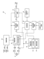
図1に本実施形態の回路装置20の構成例を示す。本実施形態の回路装置20は、発振回路30と波形整形回路40とデューティー調整回路50を含む。また後述の図13で説明するように本実施形態の発振器4は、振動子10と回路装置20を含む。振動子10は回路装置20に電気的に接続されている。例えば振動子10及び回路装置20を収納するパッケージの内部配線、ボンディグワイヤー又は金属バンプ等を用いて、振動子10と回路装置20は電気的に接続されている。
本実施形態の回路装置20は、以上に説明した構成例に限定されず、種々の変形実施が可能である。以下、本実施形態の種々の変形例について説明する。
図13に本実施形態の発振器4の構造例を示す。発振器4は、振動子10と、回路装置20と、振動子10及び回路装置20を収容するパッケージ15を有する。パッケージ15は、例えばセラミック等により形成され、その内側に収容空間を有しており、この収容空間に振動子10及び回路装置20が収容されている。収容空間は気密封止されており、望ましくは真空に近い状態である減圧状態になっている。パッケージ15により、振動子10及び回路装置20を衝撃、埃、熱、湿気等から好適に保護することができる。
ADJ…調整データ、BMP…バンプ、CB…CF1、CF2、CG…キャパシター、CK…クロック信号、CKQ…出力クロック信号、CV1…可変容量素子、CV2…可変容量素子、CX、CX1、CX2…キャパシター、IS…電流源、IVA1、IVA2、IVB1、IVB2…インバーター回路、N1…第1ノード、N2…第2ノード、VCMP…温度補償電圧、R1~Rm-1…抵抗、RB…帰還抵抗、RBS、RCP、RRF、RRFB、RRFC、RX…抵抗、TCK…クロック端子、TGND…グランド端子、TR…バイポーラートランジスター、TVDD…電源端子、TXI、TXO…端子、VBS…バイアス電圧、VDD…電源電圧、VR1~VRm-1…分圧電圧、VREF、VREFB、VREFC…基準電圧、XI、XO…発振信号
Claims (8)
- 振動子の一端に電気的に接続される第1ノードと、前記振動子の他端に電気的に接続される第2ノードとに電気的に接続され、前記振動子を発振させることで発振信号を生成する発振回路と、
前記第1ノードに接続され、前記第1ノードから前記発振信号が入力され、前記発振信号を波形整形したクロック信号を出力する波形整形回路と、
調整データに基づき可変に調整したバイアス電圧を前記第1ノードに供給することにより、前記クロック信号のデューティー比を調整するデューティー調整回路と、を含み、
前記発振回路は、
一端が前記第1ノードに接続され、容量値が固定である固定容量キャパシターと、
一端が前記固定容量キャパシターの他端に接続され、容量値が可変である可変容量素子と、を含み、
前記可変容量素子の一端及び他端の一方に温度補償電圧が入力され、
前記デューティー調整回路は、前記可変容量素子の一端及び他端の他方に基準電圧を供給することを特徴とする回路装置。 - 請求項1に記載の回路装置において、
前記デューティー調整回路は、
電源ノードとグランドノードの間に直列接続された複数の抵抗を有し、前記複数の抵抗により分圧された複数の分圧電圧を出力する分圧回路と、
前記複数の分圧電圧のいずれかである第1分圧電圧を前記バイアス電圧として選択し、前記複数の分圧電圧のいずれかである第2分圧電圧を前記基準電圧として選択する選択回路と、を含み、
前記温度補償電圧をVCMPとし、前記基準電圧をVREFとしたときに、前記複数の分圧電圧は、VCMP-VREFが0Vよりも大きくなる電圧、及び、VCMP-VREFが0V以下になる電圧を含むことを特徴とする回路装置。 - 請求項1又は2に記載の回路装置において、
前記調整データを記憶する不揮発性メモリーを含み、
前記デューティー調整回路は、
前記不揮発性メモリーに記憶された前記調整データにより設定される電圧の前記バイアス電圧を生成することを特徴とする回路装置。 - 請求項1乃至3のいずれか一項に記載の回路装置において、
前記発振回路の電源電圧は、前記波形整形回路の電源電圧以上の電圧であることを特徴とする回路装置。 - 請求項2に記載の回路装置において、
前記デューティー調整回路は、
VCMP-VREFが0Vよりも大きくなる前記基準電圧を供給することを特徴とする回路装置。 - 請求項2に記載の回路装置において、
前記デューティー調整回路は、
VCMP-VREFが0V以下になる前記基準電圧を供給することを特徴とする回路装置。 - 請求項1乃至6のいずれか一項に記載の回路装置において、
前記クロック信号をバッファリングして出力クロック信号を外部に出力する出力バッファー回路を含むことを特徴とする回路装置。 - 請求項1乃至7のいずれか一項に記載の回路装置と、
前記振動子と、
を含むことを特徴とする発振器。
Priority Applications (3)
| Application Number | Priority Date | Filing Date | Title |
|---|---|---|---|
| JP2020218552A JP7559552B2 (ja) | 2020-12-28 | 2020-12-28 | 回路装置及び発振器 |
| CN202111610006.7A CN114696793B (zh) | 2020-12-28 | 2021-12-27 | 电路装置以及振荡器 |
| US17/562,065 US12034405B2 (en) | 2020-12-28 | 2021-12-27 | Circuit device and oscillator |
Applications Claiming Priority (1)
| Application Number | Priority Date | Filing Date | Title |
|---|---|---|---|
| JP2020218552A JP7559552B2 (ja) | 2020-12-28 | 2020-12-28 | 回路装置及び発振器 |
Publications (2)
| Publication Number | Publication Date |
|---|---|
| JP2022103739A JP2022103739A (ja) | 2022-07-08 |
| JP7559552B2 true JP7559552B2 (ja) | 2024-10-02 |
Family
ID=82118291
Family Applications (1)
| Application Number | Title | Priority Date | Filing Date |
|---|---|---|---|
| JP2020218552A Active JP7559552B2 (ja) | 2020-12-28 | 2020-12-28 | 回路装置及び発振器 |
Country Status (3)
| Country | Link |
|---|---|
| US (1) | US12034405B2 (ja) |
| JP (1) | JP7559552B2 (ja) |
| CN (1) | CN114696793B (ja) |
Families Citing this family (3)
| Publication number | Priority date | Publication date | Assignee | Title |
|---|---|---|---|---|
| US20240242945A1 (en) * | 2023-01-12 | 2024-07-18 | Advanced Energy Industries, Inc. | Additional stray capacitor as another tuning knob for 1-supply ev source |
| JP2024121092A (ja) | 2023-02-27 | 2024-09-06 | セイコーエプソン株式会社 | 回路装置、発振器及び発振器の製造方法 |
| US12418283B2 (en) * | 2023-12-20 | 2025-09-16 | Qualcomm Incorporated | Programmable self-biasing inverter for correcting duty cycle distortion |
Citations (7)
| Publication number | Priority date | Publication date | Assignee | Title |
|---|---|---|---|---|
| JP2003338710A (ja) | 2001-11-02 | 2003-11-28 | Seiko Epson Corp | 発振器およびこれを用いた電子機器 |
| JP2005094644A (ja) | 2003-09-19 | 2005-04-07 | Mitsumi Electric Co Ltd | 電圧制御型発振回路 |
| JP2008035302A (ja) | 2006-07-31 | 2008-02-14 | Kawasaki Microelectronics Kk | 出力回路を備えた発振回路 |
| JP2015126280A (ja) | 2013-12-25 | 2015-07-06 | セイコーエプソン株式会社 | 発振回路、発振器、電子機器及び移動体 |
| CN107294513A (zh) | 2016-03-30 | 2017-10-24 | 中芯国际集成电路制造(上海)有限公司 | 晶体振荡器电路 |
| JP2018046460A (ja) | 2016-09-15 | 2018-03-22 | 株式会社東芝 | 無線通信装置および無線通信方法 |
| JP2018067830A (ja) | 2016-10-20 | 2018-04-26 | ルネサスエレクトロニクス株式会社 | 半導体装置 |
Family Cites Families (12)
| Publication number | Priority date | Publication date | Assignee | Title |
|---|---|---|---|---|
| US5444639A (en) * | 1993-09-07 | 1995-08-22 | Rockwell International Corporation | Angular rate sensing system and method, with digital synthesizer and variable-frequency oscillator |
| JP2003224421A (ja) | 2002-01-30 | 2003-08-08 | Seiko Epson Corp | 発振器とこれを用いた電子機器 |
| US6943636B2 (en) * | 2003-08-13 | 2005-09-13 | Agilent Technologies, Inc. | Oscillator for SERDES |
| JP5625916B2 (ja) * | 2009-02-13 | 2014-11-19 | パナソニック株式会社 | 発振回路、発振回路の製造方法、この発振回路を用いた慣性センサ及び電子機器 |
| JP2011135316A (ja) * | 2009-12-24 | 2011-07-07 | Seiko Epson Corp | 発振回路、集積回路装置及び電子機器 |
| JP6354932B2 (ja) * | 2013-10-16 | 2018-07-11 | セイコーエプソン株式会社 | 発振回路、発振器、電子機器および移動体 |
| US10298175B2 (en) * | 2016-01-06 | 2019-05-21 | Seiko Epson Corporation | Circuit device, oscillator, electronic apparatus, and vehicle |
| JP6766427B2 (ja) * | 2016-04-25 | 2020-10-14 | セイコーエプソン株式会社 | 回路装置、発振器、電子機器及び移動体 |
| CN107870556B (zh) * | 2016-09-27 | 2021-08-17 | 精工爱普生株式会社 | 集成电路装置、电子设备和移动体 |
| CN107968639A (zh) * | 2017-12-01 | 2018-04-27 | 珠海亿智电子科技有限公司 | 一种实现时钟信号占空比任意调整电路 |
| JP7331419B2 (ja) * | 2019-04-01 | 2023-08-23 | セイコーエプソン株式会社 | 集積回路装置、発振器、電子機器及び移動体 |
| JP7669779B2 (ja) * | 2021-04-30 | 2025-04-30 | セイコーエプソン株式会社 | 回路装置及び発振器 |
-
2020
- 2020-12-28 JP JP2020218552A patent/JP7559552B2/ja active Active
-
2021
- 2021-12-27 CN CN202111610006.7A patent/CN114696793B/zh active Active
- 2021-12-27 US US17/562,065 patent/US12034405B2/en active Active
Patent Citations (7)
| Publication number | Priority date | Publication date | Assignee | Title |
|---|---|---|---|---|
| JP2003338710A (ja) | 2001-11-02 | 2003-11-28 | Seiko Epson Corp | 発振器およびこれを用いた電子機器 |
| JP2005094644A (ja) | 2003-09-19 | 2005-04-07 | Mitsumi Electric Co Ltd | 電圧制御型発振回路 |
| JP2008035302A (ja) | 2006-07-31 | 2008-02-14 | Kawasaki Microelectronics Kk | 出力回路を備えた発振回路 |
| JP2015126280A (ja) | 2013-12-25 | 2015-07-06 | セイコーエプソン株式会社 | 発振回路、発振器、電子機器及び移動体 |
| CN107294513A (zh) | 2016-03-30 | 2017-10-24 | 中芯国际集成电路制造(上海)有限公司 | 晶体振荡器电路 |
| JP2018046460A (ja) | 2016-09-15 | 2018-03-22 | 株式会社東芝 | 無線通信装置および無線通信方法 |
| JP2018067830A (ja) | 2016-10-20 | 2018-04-26 | ルネサスエレクトロニクス株式会社 | 半導体装置 |
Also Published As
| Publication number | Publication date |
|---|---|
| CN114696793B (zh) | 2025-10-31 |
| US12034405B2 (en) | 2024-07-09 |
| US20220209716A1 (en) | 2022-06-30 |
| JP2022103739A (ja) | 2022-07-08 |
| CN114696793A (zh) | 2022-07-01 |
Similar Documents
| Publication | Publication Date | Title |
|---|---|---|
| CN114696793B (zh) | 电路装置以及振荡器 | |
| JP7596817B2 (ja) | 振動デバイス | |
| US12009786B2 (en) | Circuit device, oscillator, and manufacturing method | |
| US11929710B2 (en) | Oscillator | |
| US11990869B2 (en) | Circuit device and oscillator | |
| US11863124B2 (en) | Circuit device and oscillator | |
| US12388403B2 (en) | Circuit device and oscillator | |
| US12119790B2 (en) | Circuit device and oscillator | |
| US12562685B2 (en) | Circuit device and oscillator | |
| JP7815851B2 (ja) | 回路装置及び発振器 | |
| US12388400B2 (en) | Circuit device and oscillator | |
| JP7665948B2 (ja) | 発振回路、発振器及び発振回路の制御方法 | |
| JP2024108397A (ja) | 振動デバイス | |
| JP2023090099A (ja) | 回路装置及び発振器 | |
| JP2026052254A (ja) | 回路装置及び発振器 | |
| JP2022103747A (ja) | 発振器及び発振器の製造方法 |
Legal Events
| Date | Code | Title | Description |
|---|---|---|---|
| RD04 | Notification of resignation of power of attorney |
Free format text: JAPANESE INTERMEDIATE CODE: A7424 Effective date: 20210915 |
|
| RD03 | Notification of appointment of power of attorney |
Free format text: JAPANESE INTERMEDIATE CODE: A7423 Effective date: 20211104 |
|
| A621 | Written request for application examination |
Free format text: JAPANESE INTERMEDIATE CODE: A621 Effective date: 20231106 |
|
| A977 | Report on retrieval |
Free format text: JAPANESE INTERMEDIATE CODE: A971007 Effective date: 20240515 |
|
| A131 | Notification of reasons for refusal |
Free format text: JAPANESE INTERMEDIATE CODE: A131 Effective date: 20240521 |
|
| A521 | Request for written amendment filed |
Free format text: JAPANESE INTERMEDIATE CODE: A523 Effective date: 20240710 |
|
| TRDD | Decision of grant or rejection written | ||
| A01 | Written decision to grant a patent or to grant a registration (utility model) |
Free format text: JAPANESE INTERMEDIATE CODE: A01 Effective date: 20240820 |
|
| A61 | First payment of annual fees (during grant procedure) |
Free format text: JAPANESE INTERMEDIATE CODE: A61 Effective date: 20240902 |
|
| R150 | Certificate of patent or registration of utility model |
Ref document number: 7559552 Country of ref document: JP Free format text: JAPANESE INTERMEDIATE CODE: R150 |