JP7516786B2 - Semiconductor device and its manufacturing method - Google Patents
Semiconductor device and its manufacturing method Download PDFInfo
- Publication number
- JP7516786B2 JP7516786B2 JP2020040801A JP2020040801A JP7516786B2 JP 7516786 B2 JP7516786 B2 JP 7516786B2 JP 2020040801 A JP2020040801 A JP 2020040801A JP 2020040801 A JP2020040801 A JP 2020040801A JP 7516786 B2 JP7516786 B2 JP 7516786B2
- Authority
- JP
- Japan
- Prior art keywords
- substrate
- layer
- semiconductor device
- base material
- circuit element
- Prior art date
- Legal status (The legal status is an assumption and is not a legal conclusion. Google has not performed a legal analysis and makes no representation as to the accuracy of the status listed.)
- Active
Links
Images


Classifications
-
- H—ELECTRICITY
- H10—SEMICONDUCTOR DEVICES; ELECTRIC SOLID-STATE DEVICES NOT OTHERWISE PROVIDED FOR
- H10W—GENERIC PACKAGES, INTERCONNECTIONS, CONNECTORS OR OTHER CONSTRUCTIONAL DETAILS OF DEVICES COVERED BY CLASS H10
- H10W74/00—Encapsulations, e.g. protective coatings
- H10W74/10—Encapsulations, e.g. protective coatings characterised by their shape or disposition
- H10W74/131—Encapsulations, e.g. protective coatings characterised by their shape or disposition the semiconductor body being only partially enclosed
- H10W74/137—Encapsulations, e.g. protective coatings characterised by their shape or disposition the semiconductor body being only partially enclosed the encapsulations being directly on the semiconductor body
-
- H—ELECTRICITY
- H10—SEMICONDUCTOR DEVICES; ELECTRIC SOLID-STATE DEVICES NOT OTHERWISE PROVIDED FOR
- H10W—GENERIC PACKAGES, INTERCONNECTIONS, CONNECTORS OR OTHER CONSTRUCTIONAL DETAILS OF DEVICES COVERED BY CLASS H10
- H10W40/00—Arrangements for thermal protection or thermal control
- H10W40/20—Arrangements for cooling
- H10W40/22—Arrangements for cooling characterised by their shape, e.g. having conical or cylindrical projections
-
- H—ELECTRICITY
- H10—SEMICONDUCTOR DEVICES; ELECTRIC SOLID-STATE DEVICES NOT OTHERWISE PROVIDED FOR
- H10D—INORGANIC ELECTRIC SEMICONDUCTOR DEVICES
- H10D10/00—Bipolar junction transistors [BJT]
- H10D10/80—Heterojunction BJTs
-
- H—ELECTRICITY
- H10—SEMICONDUCTOR DEVICES; ELECTRIC SOLID-STATE DEVICES NOT OTHERWISE PROVIDED FOR
- H10W—GENERIC PACKAGES, INTERCONNECTIONS, CONNECTORS OR OTHER CONSTRUCTIONAL DETAILS OF DEVICES COVERED BY CLASS H10
- H10W40/00—Arrangements for thermal protection or thermal control
- H10W40/10—Arrangements for heating
-
- H—ELECTRICITY
- H10—SEMICONDUCTOR DEVICES; ELECTRIC SOLID-STATE DEVICES NOT OTHERWISE PROVIDED FOR
- H10W—GENERIC PACKAGES, INTERCONNECTIONS, CONNECTORS OR OTHER CONSTRUCTIONAL DETAILS OF DEVICES COVERED BY CLASS H10
- H10W40/00—Arrangements for thermal protection or thermal control
- H10W40/20—Arrangements for cooling
- H10W40/25—Arrangements for cooling characterised by their materials
- H10W40/253—Semiconductors
-
- H—ELECTRICITY
- H10—SEMICONDUCTOR DEVICES; ELECTRIC SOLID-STATE DEVICES NOT OTHERWISE PROVIDED FOR
- H10W—GENERIC PACKAGES, INTERCONNECTIONS, CONNECTORS OR OTHER CONSTRUCTIONAL DETAILS OF DEVICES COVERED BY CLASS H10
- H10W40/00—Arrangements for thermal protection or thermal control
- H10W40/20—Arrangements for cooling
- H10W40/25—Arrangements for cooling characterised by their materials
- H10W40/255—Arrangements for cooling characterised by their materials having a laminate or multilayered structure, e.g. direct bond copper [DBC] ceramic substrates
-
- H—ELECTRICITY
- H10—SEMICONDUCTOR DEVICES; ELECTRIC SOLID-STATE DEVICES NOT OTHERWISE PROVIDED FOR
- H10W—GENERIC PACKAGES, INTERCONNECTIONS, CONNECTORS OR OTHER CONSTRUCTIONAL DETAILS OF DEVICES COVERED BY CLASS H10
- H10W42/00—Arrangements for protection of devices
- H10W42/121—Arrangements for protection of devices protecting against mechanical damage
-
- H—ELECTRICITY
- H10—SEMICONDUCTOR DEVICES; ELECTRIC SOLID-STATE DEVICES NOT OTHERWISE PROVIDED FOR
- H10W—GENERIC PACKAGES, INTERCONNECTIONS, CONNECTORS OR OTHER CONSTRUCTIONAL DETAILS OF DEVICES COVERED BY CLASS H10
- H10W70/00—Package substrates; Interposers; Redistribution layers [RDL]
- H10W70/01—Manufacture or treatment
- H10W70/02—Manufacture or treatment of conductive package substrates serving as an interconnection, e.g. of metal plates
-
- H—ELECTRICITY
- H10—SEMICONDUCTOR DEVICES; ELECTRIC SOLID-STATE DEVICES NOT OTHERWISE PROVIDED FOR
- H10W—GENERIC PACKAGES, INTERCONNECTIONS, CONNECTORS OR OTHER CONSTRUCTIONAL DETAILS OF DEVICES COVERED BY CLASS H10
- H10W70/00—Package substrates; Interposers; Redistribution layers [RDL]
- H10W70/01—Manufacture or treatment
- H10W70/05—Manufacture or treatment of insulating or insulated package substrates, or of interposers, or of redistribution layers
- H10W70/093—Connecting or disconnecting other interconnections thereto or therefrom, e.g. connecting bond wires or bumps
-
- H—ELECTRICITY
- H10—SEMICONDUCTOR DEVICES; ELECTRIC SOLID-STATE DEVICES NOT OTHERWISE PROVIDED FOR
- H10W—GENERIC PACKAGES, INTERCONNECTIONS, CONNECTORS OR OTHER CONSTRUCTIONAL DETAILS OF DEVICES COVERED BY CLASS H10
- H10W70/00—Package substrates; Interposers; Redistribution layers [RDL]
- H10W70/60—Insulating or insulated package substrates; Interposers; Redistribution layers
- H10W70/62—Insulating or insulated package substrates; Interposers; Redistribution layers characterised by their interconnections
- H10W70/65—Shapes or dispositions of interconnections
-
- H—ELECTRICITY
- H10—SEMICONDUCTOR DEVICES; ELECTRIC SOLID-STATE DEVICES NOT OTHERWISE PROVIDED FOR
- H10W—GENERIC PACKAGES, INTERCONNECTIONS, CONNECTORS OR OTHER CONSTRUCTIONAL DETAILS OF DEVICES COVERED BY CLASS H10
- H10W72/00—Interconnections or connectors in packages
- H10W72/20—Bump connectors, e.g. solder bumps or copper pillars; Dummy bumps; Thermal bumps
-
- H—ELECTRICITY
- H10—SEMICONDUCTOR DEVICES; ELECTRIC SOLID-STATE DEVICES NOT OTHERWISE PROVIDED FOR
- H10W—GENERIC PACKAGES, INTERCONNECTIONS, CONNECTORS OR OTHER CONSTRUCTIONAL DETAILS OF DEVICES COVERED BY CLASS H10
- H10W90/00—Package configurations
- H10W90/701—Package configurations characterised by the relative positions of pads or connectors relative to package parts
-
- H—ELECTRICITY
- H10—SEMICONDUCTOR DEVICES; ELECTRIC SOLID-STATE DEVICES NOT OTHERWISE PROVIDED FOR
- H10W—GENERIC PACKAGES, INTERCONNECTIONS, CONNECTORS OR OTHER CONSTRUCTIONAL DETAILS OF DEVICES COVERED BY CLASS H10
- H10W95/00—Packaging processes not covered by the other groups of this subclass
-
- H—ELECTRICITY
- H10—SEMICONDUCTOR DEVICES; ELECTRIC SOLID-STATE DEVICES NOT OTHERWISE PROVIDED FOR
- H10D—INORGANIC ELECTRIC SEMICONDUCTOR DEVICES
- H10D10/00—Bipolar junction transistors [BJT]
- H10D10/80—Heterojunction BJTs
- H10D10/821—Vertical heterojunction BJTs
-
- H—ELECTRICITY
- H10—SEMICONDUCTOR DEVICES; ELECTRIC SOLID-STATE DEVICES NOT OTHERWISE PROVIDED FOR
- H10W—GENERIC PACKAGES, INTERCONNECTIONS, CONNECTORS OR OTHER CONSTRUCTIONAL DETAILS OF DEVICES COVERED BY CLASS H10
- H10W72/00—Interconnections or connectors in packages
- H10W72/01—Manufacture or treatment
- H10W72/012—Manufacture or treatment of bump connectors, dummy bumps or thermal bumps
- H10W72/01231—Manufacture or treatment of bump connectors, dummy bumps or thermal bumps using blanket deposition
- H10W72/01233—Manufacture or treatment of bump connectors, dummy bumps or thermal bumps using blanket deposition in liquid form, e.g. spin coating, spray coating or immersion coating
- H10W72/01235—Manufacture or treatment of bump connectors, dummy bumps or thermal bumps using blanket deposition in liquid form, e.g. spin coating, spray coating or immersion coating by plating, e.g. electroless plating or electroplating
-
- H—ELECTRICITY
- H10—SEMICONDUCTOR DEVICES; ELECTRIC SOLID-STATE DEVICES NOT OTHERWISE PROVIDED FOR
- H10W—GENERIC PACKAGES, INTERCONNECTIONS, CONNECTORS OR OTHER CONSTRUCTIONAL DETAILS OF DEVICES COVERED BY CLASS H10
- H10W72/00—Interconnections or connectors in packages
- H10W72/01—Manufacture or treatment
- H10W72/012—Manufacture or treatment of bump connectors, dummy bumps or thermal bumps
- H10W72/01251—Changing the shapes of bumps
- H10W72/01255—Changing the shapes of bumps by using masks
-
- H—ELECTRICITY
- H10—SEMICONDUCTOR DEVICES; ELECTRIC SOLID-STATE DEVICES NOT OTHERWISE PROVIDED FOR
- H10W—GENERIC PACKAGES, INTERCONNECTIONS, CONNECTORS OR OTHER CONSTRUCTIONAL DETAILS OF DEVICES COVERED BY CLASS H10
- H10W72/00—Interconnections or connectors in packages
- H10W72/01—Manufacture or treatment
- H10W72/012—Manufacture or treatment of bump connectors, dummy bumps or thermal bumps
- H10W72/01251—Changing the shapes of bumps
- H10W72/01257—Changing the shapes of bumps by reflowing
-
- H—ELECTRICITY
- H10—SEMICONDUCTOR DEVICES; ELECTRIC SOLID-STATE DEVICES NOT OTHERWISE PROVIDED FOR
- H10W—GENERIC PACKAGES, INTERCONNECTIONS, CONNECTORS OR OTHER CONSTRUCTIONAL DETAILS OF DEVICES COVERED BY CLASS H10
- H10W72/00—Interconnections or connectors in packages
- H10W72/01—Manufacture or treatment
- H10W72/019—Manufacture or treatment of bond pads
- H10W72/01931—Manufacture or treatment of bond pads using blanket deposition
- H10W72/01933—Manufacture or treatment of bond pads using blanket deposition in liquid form, e.g. spin coating, spray coating or immersion coating
- H10W72/01935—Manufacture or treatment of bond pads using blanket deposition in liquid form, e.g. spin coating, spray coating or immersion coating by plating, e.g. electroless plating or electroplating
-
- H—ELECTRICITY
- H10—SEMICONDUCTOR DEVICES; ELECTRIC SOLID-STATE DEVICES NOT OTHERWISE PROVIDED FOR
- H10W—GENERIC PACKAGES, INTERCONNECTIONS, CONNECTORS OR OTHER CONSTRUCTIONAL DETAILS OF DEVICES COVERED BY CLASS H10
- H10W72/00—Interconnections or connectors in packages
- H10W72/071—Connecting or disconnecting
- H10W72/072—Connecting or disconnecting of bump connectors
- H10W72/07231—Techniques
- H10W72/07236—Soldering or alloying
-
- H—ELECTRICITY
- H10—SEMICONDUCTOR DEVICES; ELECTRIC SOLID-STATE DEVICES NOT OTHERWISE PROVIDED FOR
- H10W—GENERIC PACKAGES, INTERCONNECTIONS, CONNECTORS OR OTHER CONSTRUCTIONAL DETAILS OF DEVICES COVERED BY CLASS H10
- H10W72/00—Interconnections or connectors in packages
- H10W72/20—Bump connectors, e.g. solder bumps or copper pillars; Dummy bumps; Thermal bumps
- H10W72/221—Structures or relative sizes
- H10W72/222—Multilayered bumps, e.g. a coating on top and side surfaces of a bump core
-
- H—ELECTRICITY
- H10—SEMICONDUCTOR DEVICES; ELECTRIC SOLID-STATE DEVICES NOT OTHERWISE PROVIDED FOR
- H10W—GENERIC PACKAGES, INTERCONNECTIONS, CONNECTORS OR OTHER CONSTRUCTIONAL DETAILS OF DEVICES COVERED BY CLASS H10
- H10W72/00—Interconnections or connectors in packages
- H10W72/20—Bump connectors, e.g. solder bumps or copper pillars; Dummy bumps; Thermal bumps
- H10W72/221—Structures or relative sizes
- H10W72/227—Multiple bumps having different sizes
-
- H—ELECTRICITY
- H10—SEMICONDUCTOR DEVICES; ELECTRIC SOLID-STATE DEVICES NOT OTHERWISE PROVIDED FOR
- H10W—GENERIC PACKAGES, INTERCONNECTIONS, CONNECTORS OR OTHER CONSTRUCTIONAL DETAILS OF DEVICES COVERED BY CLASS H10
- H10W72/00—Interconnections or connectors in packages
- H10W72/20—Bump connectors, e.g. solder bumps or copper pillars; Dummy bumps; Thermal bumps
- H10W72/241—Dispositions, e.g. layouts
-
- H—ELECTRICITY
- H10—SEMICONDUCTOR DEVICES; ELECTRIC SOLID-STATE DEVICES NOT OTHERWISE PROVIDED FOR
- H10W—GENERIC PACKAGES, INTERCONNECTIONS, CONNECTORS OR OTHER CONSTRUCTIONAL DETAILS OF DEVICES COVERED BY CLASS H10
- H10W72/00—Interconnections or connectors in packages
- H10W72/20—Bump connectors, e.g. solder bumps or copper pillars; Dummy bumps; Thermal bumps
- H10W72/251—Materials
- H10W72/252—Materials comprising solid metals or solid metalloids, e.g. PbSn, Ag or Cu
-
- H—ELECTRICITY
- H10—SEMICONDUCTOR DEVICES; ELECTRIC SOLID-STATE DEVICES NOT OTHERWISE PROVIDED FOR
- H10W—GENERIC PACKAGES, INTERCONNECTIONS, CONNECTORS OR OTHER CONSTRUCTIONAL DETAILS OF DEVICES COVERED BY CLASS H10
- H10W72/00—Interconnections or connectors in packages
- H10W72/20—Bump connectors, e.g. solder bumps or copper pillars; Dummy bumps; Thermal bumps
- H10W72/261—Functions other than electrical connecting
- H10W72/265—Providing thermal transfer, e.g. thermal bumps
-
- H—ELECTRICITY
- H10—SEMICONDUCTOR DEVICES; ELECTRIC SOLID-STATE DEVICES NOT OTHERWISE PROVIDED FOR
- H10W—GENERIC PACKAGES, INTERCONNECTIONS, CONNECTORS OR OTHER CONSTRUCTIONAL DETAILS OF DEVICES COVERED BY CLASS H10
- H10W72/00—Interconnections or connectors in packages
- H10W72/20—Bump connectors, e.g. solder bumps or copper pillars; Dummy bumps; Thermal bumps
- H10W72/261—Functions other than electrical connecting
- H10W72/267—Multiple bump connectors having different functions
-
- H—ELECTRICITY
- H10—SEMICONDUCTOR DEVICES; ELECTRIC SOLID-STATE DEVICES NOT OTHERWISE PROVIDED FOR
- H10W—GENERIC PACKAGES, INTERCONNECTIONS, CONNECTORS OR OTHER CONSTRUCTIONAL DETAILS OF DEVICES COVERED BY CLASS H10
- H10W72/00—Interconnections or connectors in packages
- H10W72/20—Bump connectors, e.g. solder bumps or copper pillars; Dummy bumps; Thermal bumps
- H10W72/29—Bond pads specially adapted therefor
-
- H—ELECTRICITY
- H10—SEMICONDUCTOR DEVICES; ELECTRIC SOLID-STATE DEVICES NOT OTHERWISE PROVIDED FOR
- H10W—GENERIC PACKAGES, INTERCONNECTIONS, CONNECTORS OR OTHER CONSTRUCTIONAL DETAILS OF DEVICES COVERED BY CLASS H10
- H10W72/00—Interconnections or connectors in packages
- H10W72/90—Bond pads, in general
- H10W72/921—Structures or relative sizes of bond pads
- H10W72/923—Bond pads having multiple stacked layers
-
- H—ELECTRICITY
- H10—SEMICONDUCTOR DEVICES; ELECTRIC SOLID-STATE DEVICES NOT OTHERWISE PROVIDED FOR
- H10W—GENERIC PACKAGES, INTERCONNECTIONS, CONNECTORS OR OTHER CONSTRUCTIONAL DETAILS OF DEVICES COVERED BY CLASS H10
- H10W72/00—Interconnections or connectors in packages
- H10W72/90—Bond pads, in general
- H10W72/921—Structures or relative sizes of bond pads
- H10W72/926—Multiple bond pads having different sizes
-
- H—ELECTRICITY
- H10—SEMICONDUCTOR DEVICES; ELECTRIC SOLID-STATE DEVICES NOT OTHERWISE PROVIDED FOR
- H10W—GENERIC PACKAGES, INTERCONNECTIONS, CONNECTORS OR OTHER CONSTRUCTIONAL DETAILS OF DEVICES COVERED BY CLASS H10
- H10W72/00—Interconnections or connectors in packages
- H10W72/90—Bond pads, in general
- H10W72/951—Materials of bond pads
- H10W72/952—Materials of bond pads comprising metals or metalloids, e.g. PbSn, Ag or Cu
-
- H—ELECTRICITY
- H10—SEMICONDUCTOR DEVICES; ELECTRIC SOLID-STATE DEVICES NOT OTHERWISE PROVIDED FOR
- H10W—GENERIC PACKAGES, INTERCONNECTIONS, CONNECTORS OR OTHER CONSTRUCTIONAL DETAILS OF DEVICES COVERED BY CLASS H10
- H10W90/00—Package configurations
- H10W90/701—Package configurations characterised by the relative positions of pads or connectors relative to package parts
- H10W90/721—Package configurations characterised by the relative positions of pads or connectors relative to package parts of bump connectors
- H10W90/724—Package configurations characterised by the relative positions of pads or connectors relative to package parts of bump connectors between a chip and a stacked insulating package substrate, interposer or RDL
Landscapes
- Wire Bonding (AREA)
- Physics & Mathematics (AREA)
- Geometry (AREA)
- Cooling Or The Like Of Semiconductors Or Solid State Devices (AREA)
- Internal Circuitry In Semiconductor Integrated Circuit Devices (AREA)
- Semiconductor Integrated Circuits (AREA)
- Engineering & Computer Science (AREA)
- Computer Networks & Wireless Communication (AREA)
- Signal Processing (AREA)
- Bipolar Transistors (AREA)
Description
本発明は、半導体装置に関し、特に、高周波回路に用いられ、発熱部を有する半導体装置及びその製造方法に関する。 The present invention relates to a semiconductor device, and in particular to a semiconductor device used in a high-frequency circuit and having a heat generating portion, and a method for manufacturing the same.
従来、バンプを介して半導体装置を実装基板に実装し、バンプを放熱経路として利用した半導体装置が知られている。 Conventionally, semiconductor devices are known that are mounted on a mounting substrate via bumps and use the bumps as a heat dissipation path.
例えば特許文献1には、化合物半導体基板に複数の単位トランジスタが並列接続されたヘテロ接合バイポーラトランジスタ(HBT)が構成された、化合物半導体装置が示されている。これら複数の単位トランジスタは化合物半導体基板に配列され、これら複数の単位トランジスタのエミッタにはバンプが電気的に接続される。
For example,
移動体通信や衛星通信等で用いられる高周波増幅回路が形成されたMMIC(Monolithic Microwave Integrated Circuit)では、近年のさらなる高速・高機能化に伴い、RFFE(RF Front-End)の損失の増加及びパワーアンプデバイスの自己発熱による特性限界が課題となっている。例えば、バイポーラトランジスタでは、そのコレクタ損失によって発熱し、バイポーラトランジスタ自体の昇温によって、ベース・エミッタ間電圧Vbeが低下し、そのことでコレクタ電流が増大し、Vbeがさらに低下する、という正帰還が掛かると熱暴走に至る。MMICの放熱性が高くないと、熱暴走しない範囲で使用可能な電力が制限されるので、結局、扱える電力とMMICのサイズとはトレードオフの関係にある。 In MMICs (Monolithic Microwave Integrated Circuits) that form high-frequency amplifier circuits used in mobile and satellite communications, etc., the increasing speed and functionality of recent years has led to issues with increased RFFE (RF Front-End) losses and performance limitations due to self-heating of power amplifier devices. For example, in bipolar transistors, heat is generated due to collector losses, and the temperature rise of the bipolar transistor itself reduces the base-emitter voltage Vbe, which in turn increases the collector current and further reduces Vbe. This positive feedback leads to thermal runaway. If the MMIC does not have high heat dissipation properties, the power that can be used without thermal runaway is limited, so ultimately there is a trade-off between the power that can be handled and the size of the MMIC.
また、RFFEモジュールにおいては、GaAs基板を用いるパワーアンプやLiTaO3基板やLiNbO3基板を用いるSAWデバイスなど、基板材料の異なるデバイスを混載するため、さらなる高性能化・小型化・低コスト化と共に、異種デバイスの集積化が求められている。 In addition, RFFE modules require the mixing of devices made from different substrate materials, such as power amplifiers that use GaAs substrates and SAW devices that use LiTaO3 or LiNbO3 substrates, so there is a demand for the integration of heterogeneous devices as well as further improvements in performance, miniaturization, and cost reduction.
そこで、本発明の目的は、高放熱性、高出力、高集積化に適した半導体装置、及びその製造方法を提供することにある。 The object of the present invention is to provide a semiconductor device suitable for high heat dissipation, high output, and high integration, and a method for manufacturing the same.
本開示の一つの態様としての半導体装置は、表面に回路素子及び当該回路素子に接続される電極を有する基板と、前記基板上に設けられ、前記回路素子又は前記電極に接続された外部接続用の導体突起部と、を備え、前記基板は、第1基材と、当該第1基材上に配置され、前記第1基材とは材料が異なる第2基材とを含み、前記回路素子及び前記電極は前記第2基材に形成され、前記第1基材は前記第2基材に比べて熱伝導率が高い。 A semiconductor device according to one aspect of the present disclosure includes a substrate having a circuit element and an electrode connected to the circuit element on its surface, and a conductor protrusion for external connection provided on the substrate and connected to the circuit element or the electrode, the substrate including a first base material and a second base material disposed on the first base material and made of a different material from the first base material, the circuit element and the electrode are formed on the second base material, and the first base material has a higher thermal conductivity than the second base material.
本開示の一つの態様としての半導体装置の製造方法は、
表面に回路素子及び当該回路素子に接続される電極を有する基板と、当該基板上に設けられ、前記回路素子又は前記電極に接して電気的に接続された外部接続用の導体突起部と、を備え、前記基板は、第1基材と、当該第1基材上に配置された第2基材とを含み、前記回路素子及び前記電極が前記第2基材に形成された、半導体装置の製造方法であって、
表面に前記回路素子及び前記電極を有する半導体薄膜を、剥離層を介して化合物半導体基材に形成する工程と、
前記剥離層をエッチングにより除去して前記半導体薄膜を前記化合物半導体基材から剥離する工程と、
前記第1基材を構成する単体半導体基材上の所定位置に、前記第2基材を構成する前記半導体薄膜を接合する工程と、
前記第2基材上に設けられ、前記回路素子又は前記電極に接続される外部接続用の導体突起部を形成する工程と、
を有する。
A method for manufacturing a semiconductor device according to one aspect of the present disclosure includes:
A method for manufacturing a semiconductor device comprising: a substrate having a circuit element and an electrode connected to the circuit element on a surface thereof; and a conductor protrusion for external connection provided on the substrate and in contact with and electrically connected to the circuit element or the electrode, the substrate including a first base material and a second base material disposed on the first base material, the circuit element and the electrode being formed on the second base material,
forming a semiconductor thin film having the circuit element and the electrode on a surface thereof on a compound semiconductor substrate via a release layer;
removing the release layer by etching to release the semiconductor thin film from the compound semiconductor substrate;
a step of bonding the semiconductor thin film constituting the second base to a predetermined position on a free-standing semiconductor base constituting the first base;
forming a conductive protrusion for external connection provided on the second base material and connected to the circuit element or the electrode;
has.
本発明によれば、放熱性が高く、そのことにより小型でありながら高出力の、又は高出力でありながら小サイズの半導体装置が得られる。 The present invention provides a semiconductor device with high heat dissipation properties, which results in a small yet high-output device, or a high-output device with a small size.
以降、図を参照して幾つかの具体的な例を挙げて、本発明を実施するための複数の形態を示す。各図中には同一箇所に同一符号を付している。要点の説明又は理解の容易性を考慮して、実施形態を説明の便宜上、複数の実施形態に分けて示すが、異なる実施形態で示した構成の部分的な置換又は組み合わせは可能である。第2の実施形態以降では第1の実施形態と共通の事柄についての記述を省略し、異なる点についてのみ説明する。特に、同様の構成による同様の作用効果については実施形態毎には逐次言及しない。 The following describes several embodiments for implementing the present invention, with reference to the drawings and some specific examples. In each drawing, the same reference numerals are used for the same parts. In consideration of the ease of explanation and understanding of the main points, the embodiments are shown divided into several embodiments for convenience of explanation, but partial substitution or combination of the configurations shown in different embodiments is possible. In the second and subsequent embodiments, descriptions of matters common to the first embodiment will be omitted, and only the differences will be described. In particular, similar effects resulting from similar configurations will not be mentioned in each embodiment.
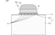
《第1の実施形態》
図1は第1の実施形態に係る半導体装置110の断面図である。この半導体装置110は、基板1と、この基板1上に設けられた第2基材側電極22に接して電気的に接続された導体ピラー23と、この導体ピラー23上に形成されたはんだ層24と、を備える。この導体ピラー23及びはんだ層24によって導体ピラーバンプPBが構成されている。
First Embodiment
1 is a cross-sectional view of a
基板1は、第1基材10と、この第1基材10上に配置された第2基材20とを含む。第2基材20には、複数の回路素子21及び当該複数の回路素子21に動作電圧を印加する又は動作電流を通電する電極が形成されている。第2基材20は、後に示すように別工程で形成され、上記回路素子は、そのエピタキシャル層上に形成されている。エピタキシャル層は例えば約3μmであり、上記電極(配線層)は約10μmである。図1において、回路素子21部に示す突起は回路素子に導通する電極である。
The
また、本実施形態では、半導体装置110は、第1基材10の表面で、第2基材20と重ならない位置に第1基材側電極12が形成されている。そして、半導体装置110は、第1基材側電極12に接続された導体ピラー13と、この導体ピラー13上に形成されたはんだ層14と、を備える。この導体ピラー13及びはんだ層14によって導体ピラーバンプPBが構成されている。
In addition, in this embodiment, the
上記導体ピラーバンプPBは、本発明に係る外部接続用の「導体突起部」に相当する。 The conductive pillar bump PB corresponds to the "conductive protrusion" for external connection according to the present invention.
この例では、第1基材10は、GaAs, AlAs, InAs, InP, GaP, InSb, GaN, InN, AlN, Si, Ge, SiC, Ga2O3, DLC(Diamond-Like Carbon), Graphite, Diamond, Glass, Sapphire, Al2O3 のいずれかを含む材料又はこれら材料のうち複数の材料からなる多元系混晶材料である。また、第2基材20は、GaAs, AlAs, InAs, InP, GaP, InSb, GaN, InN, AlN, SiGe, SiC, Ga2O3, GaBi のいずれかを含む材料又はこれら材料のうち複数の材料からなる多元系混晶材料である。ただし、第1基材10に選定する材料と第2基材20に選定する材料とは異なり、第1基材10と第2基材20との製造プロセスは異なる。基本的に、第2基材20は、例えば増幅率、遮断周波数等の所定の電気的特性が得られる材料とし、また、第1基材10は第2基材20に比べて熱伝導率が高い関係に選定する。これらのことは以降に示す別の実施形態においても同様である。
In this example, the
本実施形態では、第1基材10はSi基材であり、第2基材20はGaAs基材である。Si基材の熱伝導率は156であり、GaAs基材の熱伝導率は46である。上記回路素子21は、例えば複数の単位トランジスタが並列接続されたヘテロ接合バイポーラトランジスタ(HBT)であり、第2基材20であるGaAs基材に対するプロセスによって形成されたものである。複数の単位トランジスタのエミッタに上記導体ピラーバンプPBが電気的に接続されている。複数の単位トランジスタは第1方向(図1における左右方向)に配列され、導体ピラーバンプPBは第1方向に延伸して配置されている。
In this embodiment, the
第2基材20は第1基材10に、接合層11を介して接合されている。接合層11は例えばAu膜である。
The
上記導体ピラー13,23はCuめっき膜であり、はんだ層14,24はSnAg合金の膜である。
The
図2(A)、図2(B)は、実装基板に対する上記半導体装置110の実装構造を示す断面図である。図2(A)は、実装基板90に対して半導体装置110を実装する前段階での断面図であり、図2(B)は、実装基板90に半導体装置110を実装した後の断面図である。
2(A) and 2(B) are cross-sectional views showing the mounting structure of the
実装基板90には実装基板側電極91,92が形成されている。半導体装置110は、そのはんだ層14,24を実装基板側電極91,92に位置合わせし、加熱加圧することによって、図2(B)に示すように、半導体装置110のはんだ層14,24が実装基板側電極91,92に接続される。
Mounting
ここで、比較例としての半導体装置の構造を示す。図17は、比較例としての半導体装置が実装基板に実装された状態での断面図である。この比較例の半導体装置は、GaAs基板30に回路素子が形成されている。GaAs基板30の表面には電極32,42が形成されていて、電極42上に導体ピラー43及びはんだ層44が形成されていて、電極32上に導体ピラー33及びはんだ層34が形成されている。そして、この半導体装置は、そのはんだ層34,44が実装基板側電極91,92にそれぞれ接続されている。
Here, the structure of a semiconductor device as a comparative example is shown. FIG. 17 is a cross-sectional view of the semiconductor device as a comparative example mounted on a mounting board. In this comparative example semiconductor device, circuit elements are formed on a
なお、図1に表れているように、はんだ層24とはんだ層14との高さは第2基材20の厚み分だけ異なるが、この程度の高さの違いははんだ層14,24で吸収される。
As shown in FIG. 1, the height of
上記比較例の半導体装置と第1の実施形態に係る半導体装置110との放熱性について、図3(A)、図3(B)を参照して説明する。
The heat dissipation properties of the semiconductor device of the comparative example and the
比較例としての半導体装置では、図3(B)に示すように、回路素子に生じる熱は、破線の矢印で示すように、電極42、導体ピラー43、はんだ層44を経由して、実装基板側電極92及び実装基板90に放熱(排熱)される。
In the semiconductor device as a comparative example, as shown in FIG. 3B, heat generated in the circuit element is dissipated (exhausted) to the mounting
一方、本実施形態の半導体装置110では、図3(A)に示すように、破線の矢印で示すように、3つの熱伝導経路を経由して放熱される。第1の熱伝導経路は、回路素子が発生する熱を、第2基材側電極22、導体ピラー23、はんだ層24を経由して、実装基板側電極92及び実装基板90に放熱(排熱)する経路である。第2の熱伝導経路は、回路素子が発生する熱を、第1基材10に放熱(排熱)する経路である。第1基材10はSi基材であって、その熱伝導率は156[W/cm K]であり、GaAs基板30の熱伝導率は46[W/cm K]であり、第1基材10の熱伝導率は第2基材20の熱伝導率に比べて高い。したがって、第1基材10は高効率の熱放射体として作用する。第3の熱伝導経路は、回路素子に生じる熱を、第1基材10、第1基材側電極12、導体ピラー13、はんだ層14を経由して、実装基板側電極91及び実装基板90に放熱(排熱)する経路である。このように第1基材10は熱伝導経路として作用するので、導体ピラー13、はんだ層14、及び実装基板側電極91も熱伝導経路として作用する。
On the other hand, in the
このように構成された本実施形態の半導体装置110は次のような効果を奏する。
The
まず、3つの放熱経路が形成されることで、高い放熱性が得られる。このことで、上記HBTの自己発熱により制限されるRF特性(出力電力Pout、電力付加効率PAE)が改善される。つまり、小型でありながら高出力の半導体装置が得られる。または高出力でありながら小サイズの半導体装置が得られる。 First, by forming three heat dissipation paths, high heat dissipation is achieved. This improves the RF characteristics (output power Pout, power added efficiency PAE) that are limited by the self-heating of the HBT. In other words, a small yet high-output semiconductor device can be obtained. Or, a small-sized semiconductor device with high output can be obtained.
また、第2基材が化合物半導体の基材であることにより、その電気絶縁性を高められ、高周波特性に優れた回路を設けることができる。 In addition, since the second substrate is a compound semiconductor substrate, its electrical insulation properties are improved, making it possible to provide a circuit with excellent high-frequency characteristics.
また、第2基材20は第1基材10より薄いので、第1基材10による高い放熱効果が得られる。
In addition, since the
また、第2基材20に形成された回路素子21は動作時に発熱する発熱体であり、導体ピラーバンプPBは、発熱体としての回路素子21の直近に設けられているので、導体ピラーバンプにより、短い熱伝導経路が構成され、回路素子21が発生する熱は導体ピラーバンプPBを介して高効率で放熱される。
In addition, the
また、第2基材20は第1基材10の外縁からはみ出さないので(第1基材10より小面積であるので)、第1基材10と第2基材20とを含む基板1全体の熱抵抗が低く、第1基材10からの高い放熱効果が得られる。
In addition, since the
また、第1基材10の、第2基材20に重ならない位置の表面に第1基材側電極12が形成され、導体ピラーバンプPBは第1基材側電極12に接続されているので、第1基材側電極12に接続された導体ピラーバンプPBからの放熱効果が得られる。また、この導体ピラーバンプPBを介して、実装先である回路基板への熱伝導効率が高まり、回路基板での放熱性も高まる。
In addition, a first
次に、半導体装置110の製造方法について例示する。図4は半導体装置110の製造方法について示す図である。図4中の(1)から(7)までの図は、半導体装置110の製造途中段階における断面図であり、(8)は、完成した半導体装置110の断面図である。実際の製造はウエハー単位で行われるが、図4では、単一の半導体装置について図示している。
Next, an example of a method for manufacturing the
まず、図4中の(1)に示すように、Si基材からなる第1基材10の表面に、一般的な半導体プロセスを用いて、接合層11としてのAu膜を形成する。
First, as shown in FIG. 4 (1), an Au film is formed as a
次に、(2)に示すように、接合層11上に第2基材20を接合する。第2基材20には別工程で既に回路素子及び電極が形成されている。
Next, as shown in (2), the
次に、(3)に示すように、一般的な半導体プロセスによって、第2基材20上に第2基材側電極22を形成し、また、接合層11上に第1基材側電極12を形成する。
Next, as shown in (3), a second
次に、(4)に示すように、導体ピラー13及びはんだ層14(図1、図2(A))を形成すべき領域に開口を持つレジスト膜85を形成する。レジスト膜85の開口内に電極12,22が露出している。
Next, as shown in (4), a resist
その後、(5)(6)に示すように、レジスト膜85の開口内に露出している電極12,22の上に、めっき法により導体ピラー13,23及びはんだ層14,24を堆積させる。導体ピラー13,23はCuで形成され、その厚さは例えば40μmである。このようにして、CPB(Copper Pillar Bump)を形成する。はんだ層14,24はSnAg合金で形成され、その厚さは例えば30μmである。
After that, as shown in (5) and (6), the
その後、(7)に示すように、レジスト膜85を除去し、最後に、リフロー処理を行って、はんだ層14,24を溶融させ、その後固化させることにより、(8)に示すように半導体装置110を得る。
Then, as shown in (7), the resist
上記製造方法によれば、第2基材20は半導体薄膜であるので、低背で放熱性の高い(熱伝導率の高い)半導体装置が得られる。
According to the above manufacturing method, since the
なお、図1から図4に示した例では、接合層11としてAu膜を形成したが、例えばPt膜、Pd膜等、他の金属膜を用いることもできる。この接合層11は第2基材20に比べて熱伝導率が高いことが好ましい。このことにより、第2基材20の熱が接合層11を介して第1基材10へ高効率で排熱される。例えば、第2基材20であるGaAs基材の熱伝導率は46[W/m K]であるのに対し、Au膜の熱伝導率は319[W/m K]、Pt膜の熱伝導率は70[W/m K]、Pd膜の熱伝導率は70[W/m K]、であり、いずれも第2基材20に比べて熱伝導率が高い。
In the examples shown in Figs. 1 to 4, an Au film was formed as the
また、接合層11は第2基材20に比べて弾性率が低いことがより好ましい。第1基材10と第2基材20との線膨張係数には差があり、温度変化によって、線膨張係数の差による熱応力が生じる。しかし、接合層11が第2基材20に比べて弾性率が低いことにより、上記熱応力が低減される。このことにより、接合層11を介する、第1基材10と第2基材20との実質的な接合強度を確保できる。例えば、GaAs基材の弾性率は85.5[GPa]であるのに対し、Au膜の弾性率は78[GPa]、Al膜の弾性率は68.3[GPa]、In膜の弾性率は10.8[GPa]であり、いずれも第2基材20の弾性率より低い。
Moreover, it is more preferable that the
接合層11が金属である場合、接合層11と第2基材20との間に、接合層11と第2基材20との合金化層が形成されることが好ましい。そのことにより、より高い密着性とより高い熱伝導作用が得られる。
When the
前記接合層11は、例えばポリイミド(PI)膜、ポリベンゾオキサゾール(PBO)、ベンゾシクロブテン(BCB)等の有機材料からなる誘電体であってもよい。この接合層11は第2基材20に比べて誘電率が低いことが好ましい。第2基材20に形成されている回路素子の高周波特性として、高周波信号の伝送損失特性があるが、接合層11の誘電率が第2基材20の誘電率より高いと、接合層11の近接によって、回路素子の高周波信号の伝送損失特性が低下する。接合層11の誘電率が第2基材20の誘電率より低ければ、この伝送損失特性の低下が回避される。例えば、第2基材20であるGaAs基材の比誘電率は12.9であるのに対し、ポリイミド(PI)の誘電率は3.3、ポリベンゾオキサゾール(PBO)の誘電率は2.9、ベンゾシクロブテン(BCB)の誘電率は2.7であり、いずれも第2基材20に比べて誘電率が低い。
The
なお、接合層11は第2基材20に比べて誘電正接が小さいことが好ましい。接合層11の誘電正接が大きいと、接合層11による高周波損失が大きくなる。接合層11の誘電正接が第2基材20の誘電正接より小さければ、この高周波損失の増加が回避される。例えば、第2基材20であるGaAs基材の誘電正接は0.3であるのに対し、ポリイミド(PI)の誘電正接は0.0020、ポリベンゾオキサゾール(PBO)の誘電正接は0.0100、ベンゾシクロブテン(BCB)の誘電正接は0.0008であり、いずれも第2基材20に比べて誘電正接が小さい。
The
また、接合層11が有機材料である場合も、接合層11は第2基材20に比べて弾性率が低いことがより好ましい。このことにより、接合層11を介する、第1基材10と第2基材20との実質的な接合強度を確保できる。例えば、GaAs基材の弾性率は85.5[GPa]であるのに対し、ポリイミド(PI)の弾性率は2.5、ポリベンゾオキサゾール(PBO)の弾性率は2.8、ベンゾシクロブテン(BCB)の弾性率は2.1であり、いずれも第2基材20に比べて弾性率が低い。
Also, when the
さらには、前記接合層11は、AlN、SiC、ダイヤモンド等の絶縁体であってもよい。この接合層11は第1基材10に比べて電気抵抗率が高いことが好ましい。接合層11の電気抵抗率が第1基材10の電気抵抗率より高いと、接合層11及び第1基材10に流れる誘導電流や渦電流が抑制されるので、第2基材20に形成されている回路素子の良好な高周波特性が維持できる。
Furthermore, the
また、接合層11が絶縁体である場合も、接合層11は第1基材10に比べて熱伝導率が高いことが好ましい。このことにより、第2基材20の熱が接合層11を介して第1基材10へ高効率で排熱される。例えば、第1基材10であるSi基材の熱伝導率は156[W/cm K]であるのに対し、AlN膜の熱伝導率は170[W/cm K]、SiC膜の熱伝導率は270[W/cm K]、ダイヤモンド膜の熱伝導率は2000[W/cm K]、であり、いずれも第1基材10に比べて熱伝導率が高い。
Even when the
次に、第1の実施形態の変形例について示す。図5はこの変形例としての半導体装置111の断面図である。この半導体装置111は、図1に示した接合層11を備えていない。第2基材20は第1基材10に対して直接的に接合している。この接合は、ファンデルワールス結合又は水素結合による。その他に、静電力、共有結合、共晶合金結合等によって接合してもよい。
Next, a modified example of the first embodiment is shown. FIG. 5 is a cross-sectional view of a
第1基材側電極12は第1基材10の上面に直接形成されていて、この第1基材側電極12の上に、導体ピラー13及びはんだ層14による導体ピラーバンプPBが形成されている。
The first
このように、第1基材10に第2基材20を、接合層を介さずに接合してもよい。
In this way, the
《第2の実施形態》
第2の実施形態では、第1の実施形態とは導体突起部の構成が異なる半導体装置について示す。
Second Embodiment
In the second embodiment, a semiconductor device having a different configuration of a conductor protrusion from that in the first embodiment will be described.
図6は第2の実施形態に係る半導体装置120の断面図である。図1に示した例とは異なり、第1基材側電極12と、この第1基材側電極12に接続された外部接続用の導体突起部(導体ピラー13及びはんだ層14)とを備えない。
Figure 6 is a cross-sectional view of a
図7は、実装基板90に半導体装置120を実装した後の断面図である。実装基板90には、実装基板側電極92が形成されている。半導体装置120は、その導体ピラーバンプPBを実装基板側電極92に位置合わせし、加熱加圧することによって、はんだ層24が実装基板側電極92に接続される。
Figure 7 is a cross-sectional view of the
このような構造であっても、図中の破線の矢印で示すように、発熱部から二方向へ放熱(排熱)される。 Even with this structure, heat is dissipated (exhausted) in two directions from the heat-generating part, as shown by the dashed arrows in the figure.
《第3の実施形態》
第3の実施形態では、平坦化樹脂層を備える幾つかの半導体装置について例示する。
Third Embodiment
In the third embodiment, some semiconductor devices including a planarizing resin layer will be exemplified.
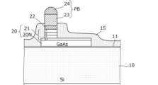
図8(A)、図8(B)は、第3の実施形態に係る半導体装置130A,130Bの断面図である。これら半導体装置130A,130Bは、第1基材10と、この第1基材10上に配置された第2基材20とを備える。第2基材20は化合物半導体の半導体基材20Nとその表面に形成されたエピタキシャル層20Dとを備える。エピタキシャル層20Dには複数の回路素子21が形成されている。
Figures 8(A) and 8(B) are cross-sectional views of
エピタキシャル層20Dの上面には、回路素子21に導通する第2基材側電極22が形成されている。第1基材10及び第2基材20の表面には平坦化樹脂層15が形成されている。第2基材側電極22の上部には、導体ピラー23及びはんだ層24による導体ピラーバンプPBが形成されている。
A second
図8(B)に示す例では、第1基材10の上面に接合層11が形成されていて、第2基材20は接合層11を介して第1基材10に接合されている。
In the example shown in FIG. 8(B), a
図9は第3の実施形態の別の半導体装置131の断面図である。この半導体装置131は、第1基材10と、この第1基材10上に配置された第2基材20とを備える。第2基材20には複数の回路素子が構成されている。第1基材10の上面には接合層11が形成されている。接合層11及び第2基材20の表面には平坦化樹脂層15が形成されている。第1基材側電極12の上部には、導体ピラー13及びはんだ層14による導体ピラーバンプPBが形成されている。
Figure 9 is a cross-sectional view of another
上記平坦化樹脂は、例えばポリイミド(PI)膜、ポリベンゾオキサゾール(PBO)、ベンゾシクロブテン(BCB)等である。このように、第1基材10及び第2基材20の表面に平坦化樹脂層15を形成することにより、相対的に厚い導体ピラー23及びはんだ層24の形成が容易となる。また、第1基材10及び第2基材20の表面がリパッシベーションされる。
The planarizing resin is, for example, a polyimide (PI) film, polybenzoxazole (PBO), benzocyclobutene (BCB), etc. In this way, by forming the
《第4の実施形態》
第4の実施形態では、複数箇所に外部接続用の導体突起を備える一つの半導体装置の例について示す。
Fourth embodiment
In the fourth embodiment, an example of one semiconductor device having conductor projections for external connection at a plurality of locations will be described.
図10は第4の実施形態に係る半導体装置140の平面図である。また、図11(A)は図10におけるA-A部分の断面図であり、図11(B)は図10におけるB-B部分の断面図である。
Figure 10 is a plan view of a
本実施形態の半導体装置140は、複数の導体ピラー上にはんだ層14,24が形成されている。図10、図11(A)に表れているように、半導体装置140の所定箇所に、それぞれ複数の単位トランジスタが、図10における左右方向に配列され、並列接続された、ヘテロ接合バイポーラトランジスタ(HBT)51A,51Bが形成されている。このHBT51A,51Bの上部に導体ピラー23及びはんだ層24による、導体ピラーバンプPBが形成されている。このHBT51A,51B、導体ピラー23及びはんだ層24の構成は第1の実施形態で示したとおりである。
In the
2つのHBT51A,51Bの両隣には、導体ピラー13及びはんだ層14による、導体ピラーバンプPBが形成されている。
A conductor pillar bump PB is formed on either side of the two
上記導体ピラーバンプPBは、図10に示すように、A-A断面以外にも形成されている。これら導体ピラーバンプPBは、上記HBT51A,51Bの近傍に配置されている。この構成により、HBT51A,51Bの発する熱が高効率で放熱される。
As shown in FIG. 10, the conductive pillar bumps PB are formed on other sections besides the A-A section. These conductive pillar bumps PB are arranged near the
半導体装置140には、上記HBT51A,51B以外にスパイラル状導体パターンによるインダクタ、誘電体層を挟んで対向する電極によるキャパシタ及び抵抗体膜のパターンによる抵抗素子等によってLCR回路が構成されている。
In addition to the
図10及び図11(B)に示すように、第1基材10の表面に接合層11が形成されていて、この接合層11の表面の所定箇所に絶縁体層16が形成されている。この絶縁体層16の表面に、スパイラルインダクタ52が形成されている。このスパイラルインダクタ52の隣接位置に、導体ピラー13及びはんだ層14による導体ピラーバンプPBが形成されている。また、図10、図11(B)に示す、半導体装置140の所定箇所には、MIMC(Metal-Insulator-Metal-Capacitor)53が形成されている。そして、このMIMC53の隣接位置に、導体ピラー13及びはんだ層14による導体ピラーバンプPBが形成されている。
As shown in Figures 10 and 11 (B), a
《第5の実施形態》
第5の実施形態では、第2基材の製造方法、及び第1基材に対する第2基材の接合方法について示す。
Fifth embodiment
In the fifth embodiment, a method for producing a second base material and a method for joining the second base material to the first base material will be described.
図12は第5の実施形態に係る各工程における斜視図である。実際の製造はウエハー単位で行われるが、図12では、単一の半導体装置について図示している。 Figure 12 is a perspective view of each process according to the fifth embodiment. Actual manufacturing is performed on a wafer basis, but Figure 12 illustrates a single semiconductor device.
図12中(1)に示すように、先ず、化合物半導体基材である母基板200に剥離層29を形成し、この剥離層29の上部に半導体薄膜をエピタキシャル成長法により形成し、この半導体薄膜に、複数の回路素子及び当該回路素子に接続される電極を形成する。この部分が後の第2基材20である。
As shown in FIG. 12 (1), first, a
次に(2)に示すように、剥離層29だけを選択的にエッチングする処理を行うことで、第2基材20(半導体薄膜片)を母基板200から剥離する。
Next, as shown in (2), a process is performed to selectively etch only the
(3)に示すように、別工程で、第1基材10に接合層11を形成し、(4)に示すように、第2基材20を接合層11表面に加圧・密着させることで、第1基材10に第2基材20を接合(ボンディング)する。つまり、半導体薄膜片を母基板200から第1基材10へ転写する。例えば、接合層11のAuが第2基材のGaAsに拡散して共晶化されることで接合される。
As shown in (3), in a separate process, a
上記第2基材20への回路素子及び電極の形成は、(1)に示す段階だけでなく、(4)に示すように、第2基材20を第1基材10へ接合した後に、第2基材20に対するプロセス(フォトリソグラフィ・エッチング工程)によって行ってもよい。
The formation of the circuit elements and electrodes on the
上記半導体薄膜片の剥離及び転写の方法は、特許第5132725号に開示されている方法を適用できる。つまり、図12中(2)に示したように、第2基材20(半導体薄膜片)を母基板200から剥離する際、第2基材20が支持体で支持された状態で、母基板200から剥離する。また、図12中(3)に示すように、第1基材10へ第2基材20を接合する際、上記支持体で支持された状態で行う。図12中の(2)(3)では、第2基材20の明示の都合上、支持体の図示を省略している。
The method of peeling and transferring the semiconductor thin film can be the method disclosed in Japanese Patent No. 5132725. That is, as shown in FIG. 12 (2), when peeling the second substrate 20 (semiconductor thin film) from the
図13は、上記半導体薄膜片の転写後、第1基材10に対する処理によって形成される半導体装置の部分断面図である。第2基材20は半導体基材20Nとその表面に形成された、バイポーラトランジスタである回路素子21とを備える。第2基材20の上部には第2基材側電極22が形成されている。この例では、第2基材側電極22はエミッタ配線である。第1基材の接合層11及び第2基材20の表面には平坦化樹脂層15が形成されている。
Figure 13 is a partial cross-sectional view of a semiconductor device formed by processing the
上記エミッタ配線である第2基材側電極22には、導体ピラー23及びはんだ層24による導体ピラーバンプPBが形成されている。
A conductor pillar bump PB made of a
半導体基材20Nもエピタキシャル層20Dも厚さは数μmである。例えば、半導体基材20Nは1μm、エピタキシャル層20Dは3μmである。従来、化合物半導体素子にワイヤーボンディングする場合に、半導体基材20N及びエピタキシャル層20Dの総厚みとして75μm以上必要であるが、本実施形態では、第1基材10の上部に付加される第2基材20の厚みは僅か数μmであるので、全体的に非常に薄型(低背)の半導体装置が構成できる。
The
《第6の実施形態》
第6の実施形態では、第1基材10と第2基材20とを接合する接合層の構造に特徴を有する半導体装置について示す。
Sixth embodiment
In the sixth embodiment, a semiconductor device having a characteristic structure of a bonding layer that bonds a
図14は第6の実施形態に係る半導体装置160の断面図である。この半導体装置160は、第1基材10と、この第1基材10上に配置された第2基材20とを備える。第2基材20は化合物半導体の半導体基材とその表面に形成されたエピタキシャル層とを備え、エピタキシャル層には複数の回路素子21が形成されている。この例では、第1基材10はSi基材であり、第2基材20はGaAs基材である。
Figure 14 is a cross-sectional view of a
第1基材10と第2基材20との間には接合層19が設けられている。つまり、第1基材10と第2基材20とは接合層19を介して接合されている。接合層19の表面には第1基材側電極12が形成されている。第2基材20の表面には第2基材側電極22が形成されている。第1基材10及び第2基材20の表面には平坦化樹脂層15が形成されている。第1基材側電極12の上部には、導体ピラー13及びはんだ層14による導体ピラーバンプPBが形成されている。第2基材側電極22の上部には、導体ピラー23及びはんだ層24による導体ピラーバンプPBが形成されている。
A
接合層19は絶縁体層17と金属層18とを含む複合材料の層である。絶縁体層17は例えばSiO2膜、SiN膜等のSi化合物の層、またはポリイミド(PI)膜等の樹脂の層である。金属層18は例えばCu膜又はAl膜である。接合層19は3層構造である。この接合層19は、第1基材10の表面に、第1層としての絶縁体層17が形成され、この絶縁体層17の表面に第2層としての金属層18が形成され、この金属層18の表面に第3層としての絶縁体層17が形成されたものである。金属層18はパターン化されていて、第2基材20の近傍と、第1基材側電極12の近傍にそれぞれ金属層18のパターンが形成されている。
The
このように、接合層19が絶縁体層17と金属層18とを含む複合材料の層であることにより、接合層19は、第1基材10と第2基材20との線膨張係数の違いに応じて生じる応力が緩和される。第1基材10、第2基材20及び接合層19の線膨張係数は次のとおりである。例えば、第1基材10であるSi基材の線膨張係数は2.60[ppm/℃]、第2基材20であるGaAs基材の線膨張係数は5.73[ppm/℃]であるのに対して、テトラエトキシシラン(TEOS)によるSiO2膜の線膨張係数は0.57[ppm/℃]、SiN膜の線膨張係数は2.30[ppm/℃]であり、第1基材10、第2基材20に比べて線膨張係数が低い。また、金属層18としてのCu膜の線膨張係数は17.0[ppm/℃]であり、第1基材10、第2基材20に比べて線膨張係数が高い。したがって、接合層19の線膨張係数は第1基材10の線膨張係数と第2基材20の線膨張係数との中間的な値となって、第2基材20と第1基材10との界面での応力が緩和される。
In this way, since the
絶縁体層17がSiO2膜、SiN膜等Si化合物の層であれば、第1基材10に対する絶縁体層17の形成が容易となり、かつ第1基材10と絶縁体層17との接合強度を高めることができる。
If the
絶縁体層17のうち、最上層のみ樹脂層であってもよい。このように、絶縁体層17の少なくとも一部が樹脂膜による層である場合は、上記線膨張係数の大小関係にかかわらず、絶縁体層17の柔軟性によって上記応力が吸収される。また、接合層19内における金属層18と絶縁体層17との間に生じる応力についても絶縁体層17で緩和することができる。
Only the top layer of the
なお、第2基材20はこの第2基材20に形成されている回路素子21の発熱・停止により膨張・収縮するが、この膨張・収縮は、回路素子21から離れた第1基材10の膨張・収縮に比べて激しい。この傾向は、第1基材10、第2基材20及び接合層19の線膨張係数が上記関係でなくても同じである。本実施形態によれば、接合層19が存在することにより、第2基材20と第1基材10との界面での応力が緩和される。
The
図15(A)、図15(B)は、半導体装置160の実装構造を示す断面図である。図15(A)は、実装基板90に対して半導体装置160を実装する前段階での断面図であり、図15(B)は、実装基板90に半導体装置160を実装した後の断面図である。
Figures 15(A) and 15(B) are cross-sectional views showing the mounting structure of the
実装基板90には実装基板側電極91,92が形成されている。半導体装置160は、そのはんだ層14,24を実装基板側電極91,92に位置合わせし、加熱加圧することによって、図15(B)に示すように、半導体装置160のはんだ層14,24が実装基板側電極91,92に接続される。
Mounting
このように、第2基材側電極22に形成されている導体ピラーバンプPBは、第2基材20に形成されている回路素子21を実装基板の回路に接続する端子として作用する。また、この第2基材側電極22に形成されている導体ピラーバンプPBは、第2基材20に形成されている回路素子21が発する熱を実装基板へ放熱する放熱用のバンプとしても作用する。
In this way, the conductive pillar bump PB formed on the second
接合層19内の金属層18は接合層19の熱伝導性を高める。したがって、第2基材20に形成されている回路素子21が発する熱は接合層19を介して第1基材10へも放熱される。また、接合層19内の金属層18は接合層19の面方向(横方向)への熱伝導性を高めるので、回路素子21が発する熱は、第1基材側電極12の近傍の金属層18を経由し、第1基材側電極12に形成されている導体ピラーバンプPBを介して実装基板90へも放熱される。また、回路素子21が発する熱は、第1基材側電極12の近傍の金属層18を経由して第1基材10へも放熱される。
The
なお、図14に示した断面では、金属層18は独立した存在であるが、第1基材側電極12に繋がっていてもよい。また、第1基材10に形成されている回路に接続されていてもよい。
In the cross section shown in FIG. 14, the
《第7の実施形態》
第7の実施形態では、第1基材10と第2基材20とを接合する接合層の構造に特徴を有する半導体装置について示す。
Seventh embodiment
In the seventh embodiment, a semiconductor device having a characteristic structure of a bonding layer that bonds a
図16は第7の実施形態に係る半導体装置170の断面図である。この半導体装置170は、第1基材10と、この第1基材10上に配置された第2基材20とを備える。第6の実施形態で図14に示した例とは接合層19の構成が異なる。その他の構成は第6の実施形態で示したとおりである。
Figure 16 is a cross-sectional view of a
接合層19は絶縁体層17と金属層18とを含む複合材料の層である。絶縁体層17は例えばSiO2膜、SiN膜等のSi化合物の層、またはポリイミド(PI)膜等の樹脂の層である。金属層18は例えばCu膜又はAl膜である。接合層19は5層構造である。図14に示した例と同様に、金属層18のパターンは、第2基材20の近傍と、第1基材側電極12の近傍にそれぞれ形成されている。
The
接合層19は次の工程で形成される。
(1)第1基材10の表面に、第1層としての絶縁体層17を形成する。
(2)その絶縁体層17の表面に第2層としての金属層18Aを形成する。
(3)この金属層18の表面に第3層としての絶縁体層17を形成する。
(4)この絶縁体層17の所定位置(下層の金属層18Aの形成位置)に開口を形成する。
(5)絶縁体層17上に金属層18Cを形成するとともに、上記開口内に金属層18Bを形成する。
(6)最上層としての絶縁体層17を形成する。
The
(1) An
(2) A
(3) An insulating
(4) An opening is formed in a predetermined position of the insulating layer 17 (where the
(5) A
(6) An insulating
本実施形態によれば、金属層18が多層構造であるので、接合層19の厚みを厚くても、接合層19の熱抵抗を低く保てる。そのため、回路素子21の放熱性が高い。また、接合層19の熱容量が大きくなるので、回路素子21の急激な発熱があっても、その温度上昇抑制効果が高い。
In this embodiment, since the
なお、第6の実施形態で述べたと同様に、金属層18は第1基材側電極12に繋がっていてもよい。また、金属層18は第1基材10に形成されている回路に接続されていてもよい。
As described in the sixth embodiment, the
実施形態毎の構成及び作用効果については以上に示したとおりであるが、実施形態で開示した態様を列挙すると、次のとおりである。 The configurations and effects of each embodiment are as described above, and the aspects disclosed in the embodiments are listed below.
本開示の一つの態様としての半導体装置は、表面に回路素子21及び当該回路素子に接続される電極を有する基板1と、この基板1上に設けられ、電極又は回路素子21に接続された外部接続用の導体ピラーバンプPBと、を備え、基板1は、第1基材10と、この第1基材10上に配置され、第1基材10とは材料が異なる第2基材20とを含み、回路素子21及び電極は第2基材20に形成され、第1基材10は第2基材20に比べて熱伝導率が高い。
A semiconductor device according to one embodiment of the present disclosure includes a
上記構成により、導体ピラーバンプPB及び第1基材10を介して放熱される。つまり両面からの放熱経路が形成されることで、高い放熱性が得られる。また、熱伝導率の高低の制限を受けない第2基材20に形成された半導体領域に回路素子が設けられるので、第2基材20の物性を有効に利用した回路が構成され、かつ第1基材10による高い放熱性が維持される。
With the above configuration, heat is dissipated through the conductive pillar bumps PB and the
本開示の一つの態様としての半導体装置は、第1基材10は単体半導体の基材であり、第2基材20は化合物半導体の基材である。このように、第1基材10が単体半導体の基材であることにより、第1基材10を介する放熱によって、全体的に高い放熱性が得られる。また、第2基材20が化合物半導体の基材であることにより、その電気絶縁性を高められ、高周波特性に優れた回路を設けることができる。
In one embodiment of the semiconductor device of the present disclosure, the
本開示の一つの態様としての半導体装置は、第2基材20は第1基材10より薄い。このことにより、第1基材10による高い放熱効果が得られる。
In one embodiment of the semiconductor device of the present disclosure, the
本開示の一つの態様としての半導体装置は、回路素子21は動作時に発熱する発熱体であり、導体ピラーバンプPBは、発熱体である回路素子21の直近に設けられている。この構成により、導体ピラーバンプPBによって短い熱伝導経路が構成され、回路素子21に生じる熱が導体ピラーバンプPBを介して効果的に放熱される。
In one aspect of the semiconductor device disclosed herein, the
本開示の一つの態様としての半導体装置は、第2基材20は第1基材10の外縁からはみ出さない。この構成により、第1基材10と第2基材20とを含む基板の熱抵抗がより低くなり、第1基材10からの高い放熱効果が得られる。
In one embodiment of the semiconductor device disclosed herein, the
本開示の一つの態様としての半導体装置は、第1基材10と第2基材20との間に、第1基材10と第2基材20とを接合する接合層11を備え、この接合層11は第2基材20に比べて熱伝導率が高い金属である。この構成により、第2基材20から第1基材10への熱伝導性が確保され、第1基材10による放熱(排熱)性が維持される。また、第1基材10から接合層11を介する放熱性が確保される。つまり、第1基材10からの放熱性は接合層11で阻害されない。
A semiconductor device according to one embodiment of the present disclosure includes a
本開示の一つの態様としての半導体装置は、接合層11は金属であり、かつ第2基材20に比べて弾性率が低い。この構成により、第1基材10と第2基材20の線膨張係数の違いにより生じる熱応力が緩和される。
In one embodiment of the semiconductor device disclosed herein, the
本開示の一つの態様としての半導体装置は、接合層11が金属であり、接合層11と第1基材10との間に、この接合層11と第1基材10との合金化層が形成される。この構成により、第1基材10と第2基材20との高い密着性及び高い熱伝導性が得られる。
In one embodiment of the semiconductor device of the present disclosure, the
本開示の一つの態様としての半導体装置は、第1基材10と第2基材20との間に接合層11を備え、この接合層11は第2基材20に比べて誘電率が低い誘電体である。この構成により、第1基材10による高周波損失が抑制され、高周波特性に優れた回路を設けることができる。
A semiconductor device according to one embodiment of the present disclosure includes a
本開示の一つの態様としての半導体装置は、接合層11が誘電体であり、かつ第2基材20に比べて弾性率が低い。この構成により、第1基材10と第2基材20の線膨張係数の違いにより生じる熱応力が緩和される。
In one embodiment of the semiconductor device of the present disclosure, the
本開示の一つの態様としての半導体装置は、第1基材10と第2基材20との間に接合層11を備え、この接合層11は第1基材10に比較して電気抵抗率が高い絶縁体である。このことにより、第1基材10と第2基材20との間の電気絶縁性が高まり、第1基材10による高周波損失が抑制され、高周波特性に優れた回路を設けることができる。
A semiconductor device according to one embodiment of the present disclosure includes a
本開示の一つの態様としての半導体装置は、接合層11が第1基材10に比べて熱伝導率が高い。このことにより、接合層11と第1基材10とにより構成される部分の実効上の熱抵抗が低くなり、高い放熱性が得られる。
In one embodiment of the semiconductor device disclosed herein, the
本開示の一つの態様としての半導体装置は、第1基材10と第2基材20との間に接合層19を備え、この接合層19は、絶縁体層17と金属層18とを含む複合材料の層である。このことにより、第1基材10と第2基材20との線膨張係数の違いにより生じる、第1基材10と第2基材20との間の応力を緩和することができる。また、第2基材20に形成されている回路素子21の発熱・停止により、第2基材20の膨張・収縮が第1基材10に比べて激しいが、そのことによって生じる、第2基材20と第1基材10との界面での応力が緩和される。
The semiconductor device according to one embodiment of the present disclosure includes a
本開示の一つの態様としての半導体装置は、第1基材10がSi基材であり、接合層19内の絶縁体層17がSi化合物の層である。このことにより、第1基材10に対する絶縁体層17の形成が容易となり、かつ第1基材10と絶縁体層17との接合強度を高めることができる。
In one embodiment of the semiconductor device of the present disclosure, the
本開示の一つの態様としての半導体装置は、絶縁体層17の少なくとも一部が樹脂である。このことにより、接合層19内における金属層18と絶縁体層17との間に生じる応力を絶縁体層17で緩和することができる。
In one embodiment of the semiconductor device of the present disclosure, at least a portion of the
本開示の一つの態様としての半導体装置は、第1基材10の、第2基材20に重ならない位置の表面に第1基材側電極12が形成され、導体ピラーバンプPBは第1基材側電極12に接続される。この構成により、第1基材側電極12に接続された導体ピラーバンプPBからの放熱効果が得られる。また、この導体ピラーバンプPBを介して、実装先である回路基板への熱伝導効率が高まり、回路基板での放熱性も高まる。
In one embodiment of the semiconductor device disclosed herein, a first
本開示の一つの態様としての半導体装置の製造方法は、表面に回路素子21及びこの回路素子21に接続される電極を有する基板1と、この基板1上に設けられ、電極又は回路素子21に接して電気的に接続された外部接続用の導体ピラーバンプPBと、を備え、基板1は、第1基材10と、この第1基材10上に配置された第2基材20とを含み、回路素子21及び電極が第2基材20に形成された、半導体装置の製造方法であって、表面に回路素子21及び電極を有する半導体薄膜を、剥離層29を介して化合物半導体の母基板200に形成する工程と、剥離層29をエッチングにより除去して半導体薄膜を化合物半導体基材の母基板200から剥離する工程と、第1基材10を構成する単体半導体基材である第1基材10上の所定位置に、第2基材20を構成する半導体薄膜を接合する工程と、第2基材20上に設けられ、電極又は回路素子21に接続される外部接続用の導体ピラーバンプPBを形成する工程と、を有する。
A method for manufacturing a semiconductor device according to one aspect of the present disclosure includes a
上記製造方法によれば、小型でありながら高出力の、又は高出力でありながら小サイズの半導体装置が得られる。 The above manufacturing method makes it possible to obtain a semiconductor device that is small yet has high output, or a semiconductor device that is small yet has high output.
最後に、上述の実施形態の説明は、すべての点で例示であって、制限的なものではない。当業者にとって変形及び変更が適宜可能である。本発明の範囲は、上述の実施形態ではなく、特許請求の範囲によって示される。さらに、本発明の範囲には、特許請求の範囲内と均等の範囲内での実施形態からの変更が含まれる。 Finally, the above-described embodiments are illustrative in all respects and are not restrictive. Those skilled in the art may make appropriate modifications and changes. The scope of the present invention is indicated by the claims, not by the above-described embodiments. Furthermore, the scope of the present invention includes modifications from the embodiments within the scope of the claims and the scope equivalent thereto.
PB…導体ピラーバンプ
1…基板
10…第1基材
11…接合層
12…第1基材側電極
15…平坦化樹脂層
16…絶縁体層
20…第2基材
20D…エピタキシャル層
20N…半導体基材
21…回路素子
22…第2基材側電極
13,23…導体ピラー
14,24…はんだ層
29…剥離層
30…GaAs基板
32,42…電極
33,43…導体ピラー
34,44…はんだ層
51A,51B…ヘテロ接合バイポーラトランジスタ
52…スパイラルインダクタ
53…MIMC
85…レジスト膜
90…実装基板
91,92…実装基板側電極
110,111,120,130A,130B,131,140,160,170…半導体装置
200…母基板
PB...
85...resist
Claims (13)
前記基板上に設けられ、前記回路素子又は前記電極に接続された外部接続用の導体突起部と、
を備え、
前記基板は、第1基材と、当該第1基材上に配置され、前記第1基材とは材料が異なる第2基材とを含み、
前記回路素子及び前記電極は前記第2基材に形成され、
前記第1基材と前記第2基材との間に、前記第1基材と前記第2基材とを接合する接合層を備え、
前記第1基材は前記第2基材に比べて熱伝導率が高く、
前記接合層は前記第2基材に比べて熱伝導率が高く、
前記接合層は前記第1基材に比較して電気抵抗率が高い絶縁体である、
半導体装置。 a substrate having a circuit element and an electrode connected to the circuit element on a surface thereof;
a conductor protrusion for external connection provided on the substrate and connected to the circuit element or the electrode;
Equipped with
The substrate includes a first substrate and a second substrate disposed on the first substrate and made of a different material than the first substrate;
the circuit element and the electrode are formed on the second substrate;
a bonding layer is provided between the first base material and the second base material to bond the first base material and the second base material;
the first base material has a higher thermal conductivity than the second base material;
The bonding layer has a higher thermal conductivity than the second base material,
The bonding layer is an insulator having a higher electrical resistivity than the first base material.
Semiconductor device.
前記基板上に設けられ、前記回路素子又は前記電極に接続された外部接続用の導体突起部と、a conductor protrusion for external connection provided on the substrate and connected to the circuit element or the electrode;
を備え、Equipped with
前記基板は、第1基材と、当該第1基材上に配置され、前記第1基材とは材料が異なる第2基材とを含み、The substrate includes a first substrate and a second substrate disposed on the first substrate and made of a different material than the first substrate;
前記回路素子及び前記電極は前記第2基材に形成され、the circuit element and the electrode are formed on the second substrate;
前記第1基材と前記第2基材との間に、前記第1基材と前記第2基材とを接合する接合層を備え、a bonding layer is provided between the first base material and the second base material to bond the first base material and the second base material;
前記第1基材は前記第2基材に比べて熱伝導率が高く、the first base material has a higher thermal conductivity than the second base material;
前記接合層は前記第2基材に比べて熱伝導率が高く、The bonding layer has a higher thermal conductivity than the second base material,
前記接合層は、絶縁体層と金属層とを含む複合材料の層である、The bonding layer is a layer of a composite material including an insulator layer and a metal layer.
半導体装置。Semiconductor device.
前記第2基材は化合物半導体の基材である、
請求項1または請求項2に記載の半導体装置。 the first substrate is a substrate of a single semiconductor;
The second substrate is a compound semiconductor substrate.
3. The semiconductor device according to claim 1 or 2 .
請求項1乃至請求項3のいずれかに記載の半導体装置。 The second substrate is thinner than the first substrate.
4. The semiconductor device according to claim 1.
請求項1乃至請求項4のいずれかに記載の半導体装置。 the circuit element is a heat generating element that generates heat during operation, and the conductor protrusion portion is provided in close proximity to the circuit element that is the heat generating element;
5. The semiconductor device according to claim 1.
請求項1乃至請求項5のいずれかに記載の半導体装置。 The second substrate does not extend beyond the outer edge of the first substrate.
6. The semiconductor device according to claim 1,
請求項1に記載の半導体装置。 The bonding layer has a higher thermal conductivity than the first base material.
The semiconductor device according to claim 1 .
前記絶縁体層はSi化合物の層である、
請求項2に記載の半導体装置。 The first substrate is a Si substrate;
The insulator layer is a layer of a Si compound.
The semiconductor device according to claim 2 .
請求項2に記載の半導体装置。 At least a portion of the insulator layer is made of resin .
The semiconductor device according to claim 2 .
前記導体突起部は前記第1基材側電極に接続された、
請求項1乃至請求項9のいずれかに記載の半導体装置。 a first substrate side electrode is formed on a surface of the first substrate at a position not overlapping the second substrate;
The conductor protrusion is connected to the first substrate side electrode.
10. The semiconductor device according to claim 1.
請求項1乃至請求項10のいずれかに記載の半導体装置。 The conductor protrusion portion is a conductor pillar having a solder layer formed on a conductor pillar.
The semiconductor device according to claim 1 .
表面に前記回路素子及び前記電極を有する半導体薄膜を、剥離層を介して化合物半導体基材に形成する工程と、
前記剥離層をエッチングにより除去して前記半導体薄膜を前記化合物半導体基材から剥離する工程と、
前記第2基材に比べて熱伝導率が高い前記第1基材を構成する単体半導体基材上の所定位置に、前記第2基材に比べて熱伝導率が高く、前記第1基材に比較して電気抵抗率が高い絶縁体である接合層を用いて、前記第2基材を構成する前記半導体薄膜を接合する工程と、
前記第2基材上に設けられ、前記回路素子又は前記電極に接続される外部接続用の導体突起部を形成する工程と、
を有する半導体装置の製造方法。 A method for manufacturing a semiconductor device comprising: a substrate having a circuit element and an electrode connected to the circuit element on a surface thereof; and a conductor protrusion for external connection provided on the substrate and in contact with and electrically connected to the circuit element or the electrode, the substrate including a first base material and a second base material disposed on the first base material, the circuit element and the electrode being formed on the second base material,
forming a semiconductor thin film having the circuit element and the electrode on a surface thereof on a compound semiconductor substrate via a release layer;
removing the release layer by etching to release the semiconductor thin film from the compound semiconductor substrate;
a step of bonding the semiconductor thin film constituting the second base to a predetermined position on a single semiconductor base constituting the first base, the single semiconductor base having a higher thermal conductivity than the second base, by using a bonding layer which is an insulator having a higher thermal conductivity than the second base and a higher electrical resistivity than the first base;
forming a conductive protrusion for external connection provided on the second base material and connected to the circuit element or the electrode;
A method for manufacturing a semiconductor device having the above structure.
表面に前記回路素子及び前記電極を有する半導体薄膜を、剥離層を介して化合物半導体基材に形成する工程と、forming a semiconductor thin film having the circuit element and the electrode on a surface thereof on a compound semiconductor substrate via a release layer;
前記剥離層をエッチングにより除去して前記半導体薄膜を前記化合物半導体基材から剥離する工程と、removing the release layer by etching to release the semiconductor thin film from the compound semiconductor substrate;
前記第2基材に比べて熱伝導率が高い前記第1基材を構成する単体半導体基材上の所定位置に、前記第2基材に比べて熱伝導率が高く、絶縁体層と金属層とを含む複合材料の層である接合層を用いて、前記第2基材を構成する前記半導体薄膜を接合する工程と、a step of bonding the semiconductor thin film constituting the second base to a predetermined position on a single semiconductor substrate constituting the first base having a higher thermal conductivity than the second base, using a bonding layer which is a layer of a composite material having a higher thermal conductivity than the second base and which includes an insulator layer and a metal layer;
前記第2基材上に設けられ、前記回路素子又は前記電極に接続される外部接続用の導体突起部を形成する工程と、forming a conductive protrusion for external connection provided on the second base material and connected to the circuit element or the electrode;
を有する半導体装置の製造方法。A method for manufacturing a semiconductor device having the above structure.
Priority Applications (17)
| Application Number | Priority Date | Filing Date | Title |
|---|---|---|---|
| JP2020040801A JP7516786B2 (en) | 2019-06-21 | 2020-03-10 | Semiconductor device and its manufacturing method |
| TW113136387A TWI915980B (en) | 2019-06-21 | 2020-05-14 | Semiconductor device |
| TW112130657A TWI854787B (en) | 2019-06-21 | 2020-05-14 | Semiconductor device |
| TW113118768A TWI879574B (en) | 2019-06-21 | 2020-05-14 | Semiconductor device |
| TW109116022A TWI825318B (en) | 2019-06-21 | 2020-05-14 | Semiconductor device and method for producing the same |
| US16/901,980 US11677018B2 (en) | 2019-06-21 | 2020-06-15 | Semiconductor device and method for producing the same |
| CN202411653853.5A CN119694993A (en) | 2019-06-21 | 2020-06-19 | Semiconductor devices |
| CN202411653966.5A CN119694995A (en) | 2019-06-21 | 2020-06-19 | Semiconductor devices |
| CN202010564522.XA CN112117246A (en) | 2019-06-21 | 2020-06-19 | Semiconductor device and method for manufacturing the same |
| CN202411653903.XA CN119694994A (en) | 2019-06-21 | 2020-06-19 | Semiconductor devices |
| CN202411653284.4A CN119694992A (en) | 2019-06-21 | 2020-06-19 | Semiconductor devices |
| US18/296,778 US12136664B2 (en) | 2019-06-21 | 2023-04-06 | Semiconductor device and method for producing the same |
| JP2024077830A JP7677497B2 (en) | 2019-06-21 | 2024-05-13 | Semiconductor device and its manufacturing method |
| US18/903,862 US20250022942A1 (en) | 2019-06-21 | 2024-10-01 | Semiconductor device and method for producing the same |
| JP2025074306A JP2025114644A (en) | 2019-06-21 | 2025-04-28 | Semiconductor Devices |
| JP2025074305A JP2025114643A (en) | 2019-06-21 | 2025-04-28 | Semiconductor Devices |
| JP2025074304A JP2025114642A (en) | 2019-06-21 | 2025-04-28 | Semiconductor Devices |
Applications Claiming Priority (3)
| Application Number | Priority Date | Filing Date | Title |
|---|---|---|---|
| JP2019115560 | 2019-06-21 | ||
| JP2019115560 | 2019-06-21 | ||
| JP2020040801A JP7516786B2 (en) | 2019-06-21 | 2020-03-10 | Semiconductor device and its manufacturing method |
Related Child Applications (1)
| Application Number | Title | Priority Date | Filing Date |
|---|---|---|---|
| JP2024077830A Division JP7677497B2 (en) | 2019-06-21 | 2024-05-13 | Semiconductor device and its manufacturing method |
Publications (3)
| Publication Number | Publication Date |
|---|---|
| JP2021002644A JP2021002644A (en) | 2021-01-07 |
| JP2021002644A5 JP2021002644A5 (en) | 2022-11-17 |
| JP7516786B2 true JP7516786B2 (en) | 2024-07-17 |
Family
ID=73798971
Family Applications (5)
| Application Number | Title | Priority Date | Filing Date |
|---|---|---|---|
| JP2020040801A Active JP7516786B2 (en) | 2019-06-21 | 2020-03-10 | Semiconductor device and its manufacturing method |
| JP2024077830A Active JP7677497B2 (en) | 2019-06-21 | 2024-05-13 | Semiconductor device and its manufacturing method |
| JP2025074304A Pending JP2025114642A (en) | 2019-06-21 | 2025-04-28 | Semiconductor Devices |
| JP2025074305A Pending JP2025114643A (en) | 2019-06-21 | 2025-04-28 | Semiconductor Devices |
| JP2025074306A Pending JP2025114644A (en) | 2019-06-21 | 2025-04-28 | Semiconductor Devices |
Family Applications After (4)
| Application Number | Title | Priority Date | Filing Date |
|---|---|---|---|
| JP2024077830A Active JP7677497B2 (en) | 2019-06-21 | 2024-05-13 | Semiconductor device and its manufacturing method |
| JP2025074304A Pending JP2025114642A (en) | 2019-06-21 | 2025-04-28 | Semiconductor Devices |
| JP2025074305A Pending JP2025114643A (en) | 2019-06-21 | 2025-04-28 | Semiconductor Devices |
| JP2025074306A Pending JP2025114644A (en) | 2019-06-21 | 2025-04-28 | Semiconductor Devices |
Country Status (4)
| Country | Link |
|---|---|
| US (3) | US11677018B2 (en) |
| JP (5) | JP7516786B2 (en) |
| CN (5) | CN119694992A (en) |
| TW (3) | TWI825318B (en) |
Families Citing this family (4)
| Publication number | Priority date | Publication date | Assignee | Title |
|---|---|---|---|---|
| JP7516786B2 (en) | 2019-06-21 | 2024-07-17 | 株式会社村田製作所 | Semiconductor device and its manufacturing method |
| CN113517209A (en) * | 2020-04-10 | 2021-10-19 | 长鑫存储技术有限公司 | Semiconductor structure and method of forming the same |
| WO2022259923A1 (en) * | 2021-06-11 | 2022-12-15 | 株式会社村田製作所 | Semiconductor device |
| US20250080063A1 (en) * | 2023-09-06 | 2025-03-06 | Wolfspeed, Inc. | Transistor with gate layout, device implementing the transistor with output pre-matching, and process of implementing the same |
Citations (5)
| Publication number | Priority date | Publication date | Assignee | Title |
|---|---|---|---|---|
| JP2009190918A (en) | 2008-02-13 | 2009-08-27 | New Japan Radio Co Ltd | Nitride semiconductor substrate manufacturing method and nitride semiconductor device manufacturing method |
| JP2012169586A (en) | 2011-01-24 | 2012-09-06 | Fujitsu Ltd | Heat spreader and manufacturing method therefor, semiconductor device, electronic device |
| JP2013191655A (en) | 2012-03-13 | 2013-09-26 | Nippon Telegr & Teleph Corp <Ntt> | Heterojunction bipolar transistor and manufacturing method of the same |
| JP2019009409A (en) | 2017-06-28 | 2019-01-17 | 株式会社村田製作所 | Semiconductor chip |
| JP2019075536A (en) | 2017-10-11 | 2019-05-16 | 株式会社村田製作所 | Power amplifier module |
Family Cites Families (32)
| Publication number | Priority date | Publication date | Assignee | Title |
|---|---|---|---|---|
| JPH05190488A (en) * | 1991-07-10 | 1993-07-30 | Nec Corp | Ohmic electrode manufacturing method |
| US7247892B2 (en) * | 2000-04-24 | 2007-07-24 | Taylor Geoff W | Imaging array utilizing thyristor-based pixel elements |
| JP4701506B2 (en) * | 2000-09-14 | 2011-06-15 | ソニー株式会社 | Circuit block body manufacturing method, wiring circuit device manufacturing method, and semiconductor device manufacturing method |
| JP2003229366A (en) * | 2002-02-05 | 2003-08-15 | Matsushita Electric Ind Co Ltd | Semiconductor laminated structure |
| JP2005129825A (en) * | 2003-10-27 | 2005-05-19 | Sumitomo Chemical Co Ltd | Method for manufacturing compound semiconductor substrate |
| KR100687758B1 (en) * | 2005-12-08 | 2007-02-27 | 한국전자통신연구원 | Heterojunction bipolar transistor and method for manufacturing same |
| JP2008204968A (en) * | 2007-02-16 | 2008-09-04 | Furukawa Electric Co Ltd:The | Semiconductor package substrate and manufacturing method thereof |
| JP2010206020A (en) * | 2009-03-04 | 2010-09-16 | Panasonic Corp | Semiconductor device |
| US20100270591A1 (en) * | 2009-04-27 | 2010-10-28 | University Of Seoul Industry Cooperation Foundation | High-electron mobility transistor |
| CN102714176A (en) * | 2010-02-26 | 2012-10-03 | 住友化学株式会社 | Electronic device and method for manufacturing electronic device |
| JP2012089828A (en) * | 2010-09-22 | 2012-05-10 | Toshiba Corp | Semiconductor device manufacturing method |
| US8772817B2 (en) * | 2010-12-22 | 2014-07-08 | Cree, Inc. | Electronic device submounts including substrates with thermally conductive vias |
| DE112012006007T5 (en) * | 2012-03-09 | 2014-11-20 | Mitsubishi Electric Corp. | Semiconductor module |
| JP6307832B2 (en) * | 2013-01-22 | 2018-04-11 | 三菱マテリアル株式会社 | Power module board, power module board with heat sink, power module with heat sink |
| JP6120704B2 (en) * | 2013-07-03 | 2017-04-26 | 三菱電機株式会社 | Semiconductor device |
| JP6004343B2 (en) * | 2013-09-13 | 2016-10-05 | 日本電信電話株式会社 | Manufacturing method of semiconductor device |
| JP2015065241A (en) * | 2013-09-24 | 2015-04-09 | ルネサスエレクトロニクス株式会社 | Method of manufacturing semiconductor device and semiconductor device |
| JP2015144248A (en) * | 2013-12-25 | 2015-08-06 | キヤノン株式会社 | Semiconductor device, and method for manufacturing the same |
| KR102019914B1 (en) * | 2014-06-11 | 2019-11-04 | 엘지이노텍 주식회사 | Light Emitting Device |
| US20160141220A1 (en) * | 2014-11-18 | 2016-05-19 | Sumitomo Electric Industries, Ltd. | Hetero-bipolar transistor and method for producing the same |
| JP6071009B2 (en) * | 2014-11-27 | 2017-02-01 | 株式会社村田製作所 | Compound semiconductor device |
| JP2016171172A (en) * | 2015-03-12 | 2016-09-23 | 日本電信電話株式会社 | Heterojunction bipolar transistor and method of manufacturing the same |
| JP6415381B2 (en) * | 2015-04-30 | 2018-10-31 | 三菱電機株式会社 | Manufacturing method of semiconductor device |
| JP6348451B2 (en) | 2015-05-25 | 2018-06-27 | 日本電信電話株式会社 | Heterojunction bipolar transistor |
| CN107771352B (en) * | 2015-06-26 | 2022-05-10 | 英特尔公司 | Designed GAN devices on silicon substrates |
| US20180309025A1 (en) * | 2015-10-29 | 2018-10-25 | Kyocera Corporation | Light-emitting device, light receiving and emitting device module, and optical sensor |
| JP2018026406A (en) * | 2016-08-08 | 2018-02-15 | 株式会社村田製作所 | Heterojunction bipolar transistor |
| US9997590B2 (en) * | 2016-10-24 | 2018-06-12 | International Büsiness Machines Corporation | FinFET resistor and method to fabricate same |
| US10847436B2 (en) * | 2017-10-11 | 2020-11-24 | Murata Manufacturing Co., Ltd. | Power amplifier module |
| JP2019102724A (en) * | 2017-12-06 | 2019-06-24 | 株式会社村田製作所 | Semiconductor element |
| CN108598158B (en) * | 2018-03-09 | 2019-06-07 | 苏州闻颂智能科技有限公司 | A kind of cascode Heterojunction Bipolar Transistors |
| JP7516786B2 (en) | 2019-06-21 | 2024-07-17 | 株式会社村田製作所 | Semiconductor device and its manufacturing method |
-
2020
- 2020-03-10 JP JP2020040801A patent/JP7516786B2/en active Active
- 2020-05-14 TW TW109116022A patent/TWI825318B/en active
- 2020-05-14 TW TW112130657A patent/TWI854787B/en active
- 2020-05-14 TW TW113118768A patent/TWI879574B/en active
- 2020-06-15 US US16/901,980 patent/US11677018B2/en active Active
- 2020-06-19 CN CN202411653284.4A patent/CN119694992A/en active Pending
- 2020-06-19 CN CN202411653853.5A patent/CN119694993A/en active Pending
- 2020-06-19 CN CN202411653966.5A patent/CN119694995A/en active Pending
- 2020-06-19 CN CN202411653903.XA patent/CN119694994A/en active Pending
- 2020-06-19 CN CN202010564522.XA patent/CN112117246A/en active Pending
-
2023
- 2023-04-06 US US18/296,778 patent/US12136664B2/en active Active
-
2024
- 2024-05-13 JP JP2024077830A patent/JP7677497B2/en active Active
- 2024-10-01 US US18/903,862 patent/US20250022942A1/en active Pending
-
2025
- 2025-04-28 JP JP2025074304A patent/JP2025114642A/en active Pending
- 2025-04-28 JP JP2025074305A patent/JP2025114643A/en active Pending
- 2025-04-28 JP JP2025074306A patent/JP2025114644A/en active Pending
Patent Citations (5)
| Publication number | Priority date | Publication date | Assignee | Title |
|---|---|---|---|---|
| JP2009190918A (en) | 2008-02-13 | 2009-08-27 | New Japan Radio Co Ltd | Nitride semiconductor substrate manufacturing method and nitride semiconductor device manufacturing method |
| JP2012169586A (en) | 2011-01-24 | 2012-09-06 | Fujitsu Ltd | Heat spreader and manufacturing method therefor, semiconductor device, electronic device |
| JP2013191655A (en) | 2012-03-13 | 2013-09-26 | Nippon Telegr & Teleph Corp <Ntt> | Heterojunction bipolar transistor and manufacturing method of the same |
| JP2019009409A (en) | 2017-06-28 | 2019-01-17 | 株式会社村田製作所 | Semiconductor chip |
| JP2019075536A (en) | 2017-10-11 | 2019-05-16 | 株式会社村田製作所 | Power amplifier module |
Also Published As
| Publication number | Publication date |
|---|---|
| JP2025114644A (en) | 2025-08-05 |
| TW202504100A (en) | 2025-01-16 |
| JP2021002644A (en) | 2021-01-07 |
| JP2025114643A (en) | 2025-08-05 |
| US11677018B2 (en) | 2023-06-13 |
| CN112117246A (en) | 2020-12-22 |
| US12136664B2 (en) | 2024-11-05 |
| TWI825318B (en) | 2023-12-11 |
| TW202101762A (en) | 2021-01-01 |
| US20230246094A1 (en) | 2023-08-03 |
| JP2025114642A (en) | 2025-08-05 |
| US20250022942A1 (en) | 2025-01-16 |
| CN119694995A (en) | 2025-03-25 |
| US20200403088A1 (en) | 2020-12-24 |
| CN119694993A (en) | 2025-03-25 |
| TW202435452A (en) | 2024-09-01 |
| JP2024102316A (en) | 2024-07-30 |
| CN119694992A (en) | 2025-03-25 |
| JP7677497B2 (en) | 2025-05-15 |
| TWI854787B (en) | 2024-09-01 |
| TW202349706A (en) | 2023-12-16 |
| CN119694994A (en) | 2025-03-25 |
| TWI879574B (en) | 2025-04-01 |
Similar Documents
| Publication | Publication Date | Title |
|---|---|---|
| JP7677497B2 (en) | Semiconductor device and its manufacturing method | |
| TWI333278B (en) | Group iii nitride bases flip-chip integrated circuit and method for fabricating | |
| JP2021197447A (en) | Semiconductor device | |
| JP2004319552A (en) | Flip chip type facing electrode HEMT | |
| JP7625825B2 (en) | Semiconductor Device | |
| JP7608814B2 (en) | RF circuit module and its manufacturing method | |
| US12199083B2 (en) | RF circuit module and manufacturing method therefor | |
| TWI915980B (en) | Semiconductor device | |
| JP3744828B2 (en) | Semiconductor device | |
| JP2012209334A (en) | Low-profile millimeter waveband package and method of manufacturing the same | |
| JP5562898B2 (en) | Semiconductor device and manufacturing method thereof | |
| WO2019208295A1 (en) | Bipolar transistor and production method therefor | |
| JP2010186962A (en) | Semiconductor package, and method of fabricating the same | |
| JPH09246812A (en) | High frequency semiconductor device | |
| JPS5929377Y2 (en) | High frequency high power transistor device | |
| TW202601943A (en) | Surface mount power device and fabrication method thereof | |
| WO2024202593A1 (en) | Compound semiconductor amplifier and circuit module |
Legal Events
| Date | Code | Title | Description |
|---|---|---|---|
| A521 | Request for written amendment filed |
Free format text: JAPANESE INTERMEDIATE CODE: A523 Effective date: 20221109 |
|
| A621 | Written request for application examination |
Free format text: JAPANESE INTERMEDIATE CODE: A621 Effective date: 20221109 |
|
| A977 | Report on retrieval |
Free format text: JAPANESE INTERMEDIATE CODE: A971007 Effective date: 20230823 |
|
| A131 | Notification of reasons for refusal |
Free format text: JAPANESE INTERMEDIATE CODE: A131 Effective date: 20230926 |
|
| A521 | Request for written amendment filed |
Free format text: JAPANESE INTERMEDIATE CODE: A523 Effective date: 20231124 |
|
| A02 | Decision of refusal |
Free format text: JAPANESE INTERMEDIATE CODE: A02 Effective date: 20240213 |
|
| A521 | Request for written amendment filed |
Free format text: JAPANESE INTERMEDIATE CODE: A523 Effective date: 20240513 |
|
| A911 | Transfer to examiner for re-examination before appeal (zenchi) |
Free format text: JAPANESE INTERMEDIATE CODE: A911 Effective date: 20240520 |
|
| TRDD | Decision of grant or rejection written | ||
| A01 | Written decision to grant a patent or to grant a registration (utility model) |
Free format text: JAPANESE INTERMEDIATE CODE: A01 Effective date: 20240604 |
|
| A61 | First payment of annual fees (during grant procedure) |
Free format text: JAPANESE INTERMEDIATE CODE: A61 Effective date: 20240617 |
|
| R150 | Certificate of patent or registration of utility model |
Ref document number: 7516786 Country of ref document: JP Free format text: JAPANESE INTERMEDIATE CODE: R150 |