JP2015144248A - Semiconductor device, and method for manufacturing the same - Google Patents
Semiconductor device, and method for manufacturing the same Download PDFInfo
- Publication number
- JP2015144248A JP2015144248A JP2014245236A JP2014245236A JP2015144248A JP 2015144248 A JP2015144248 A JP 2015144248A JP 2014245236 A JP2014245236 A JP 2014245236A JP 2014245236 A JP2014245236 A JP 2014245236A JP 2015144248 A JP2015144248 A JP 2015144248A
- Authority
- JP
- Japan
- Prior art keywords
- mos transistor
- type mos
- layer
- semiconductor device
- semiconductor layer
- Prior art date
- Legal status (The legal status is an assumption and is not a legal conclusion. Google has not performed a legal analysis and makes no representation as to the accuracy of the status listed.)
- Pending
Links
- 239000004065 semiconductor Substances 0.000 title claims abstract description 191
- 238000000034 method Methods 0.000 title claims description 209
- 238000004519 manufacturing process Methods 0.000 title claims description 23
- 239000000758 substrate Substances 0.000 claims abstract description 152
- 238000001514 detection method Methods 0.000 claims abstract description 90
- 230000004888 barrier function Effects 0.000 claims abstract description 77
- 239000012535 impurity Substances 0.000 claims abstract description 59
- 238000009792 diffusion process Methods 0.000 claims abstract description 45
- XUIMIQQOPSSXEZ-UHFFFAOYSA-N Silicon Chemical compound [Si] XUIMIQQOPSSXEZ-UHFFFAOYSA-N 0.000 claims abstract description 38
- 239000000203 mixture Substances 0.000 claims abstract description 38
- 229910052710 silicon Inorganic materials 0.000 claims abstract description 38
- 239000010703 silicon Substances 0.000 claims abstract description 38
- 230000008569 process Effects 0.000 claims description 142
- 229910052751 metal Inorganic materials 0.000 claims description 55
- 239000002184 metal Substances 0.000 claims description 53
- 230000015572 biosynthetic process Effects 0.000 claims description 19
- 238000003384 imaging method Methods 0.000 claims description 15
- 238000005229 chemical vapour deposition Methods 0.000 claims description 9
- 238000001451 molecular beam epitaxy Methods 0.000 claims description 5
- 238000013461 design Methods 0.000 abstract description 5
- 239000010410 layer Substances 0.000 description 205
- 238000002955 isolation Methods 0.000 description 26
- 239000000463 material Substances 0.000 description 19
- 238000010438 heat treatment Methods 0.000 description 16
- 229910000577 Silicon-germanium Inorganic materials 0.000 description 15
- 238000005468 ion implantation Methods 0.000 description 15
- 239000005380 borophosphosilicate glass Substances 0.000 description 14
- 239000010936 titanium Substances 0.000 description 13
- 239000013078 crystal Substances 0.000 description 12
- 229910021420 polycrystalline silicon Inorganic materials 0.000 description 12
- 229920005591 polysilicon Polymers 0.000 description 12
- 238000005530 etching Methods 0.000 description 11
- 230000004913 activation Effects 0.000 description 10
- 238000000137 annealing Methods 0.000 description 10
- 230000003647 oxidation Effects 0.000 description 9
- 238000007254 oxidation reaction Methods 0.000 description 9
- 238000012545 processing Methods 0.000 description 9
- 238000000926 separation method Methods 0.000 description 8
- BOTDANWDWHJENH-UHFFFAOYSA-N Tetraethyl orthosilicate Chemical compound CCO[Si](OCC)(OCC)OCC BOTDANWDWHJENH-UHFFFAOYSA-N 0.000 description 7
- 230000007547 defect Effects 0.000 description 6
- 239000011521 glass Substances 0.000 description 6
- 150000004767 nitrides Chemical class 0.000 description 6
- JBRZTFJDHDCESZ-UHFFFAOYSA-N AsGa Chemical compound [As]#[Ga] JBRZTFJDHDCESZ-UHFFFAOYSA-N 0.000 description 5
- 229910001218 Gallium arsenide Inorganic materials 0.000 description 5
- ATJFFYVFTNAWJD-UHFFFAOYSA-N Tin Chemical compound [Sn] ATJFFYVFTNAWJD-UHFFFAOYSA-N 0.000 description 5
- 150000001875 compounds Chemical class 0.000 description 5
- 238000010586 diagram Methods 0.000 description 5
- KRHYYFGTRYWZRS-UHFFFAOYSA-N Fluorane Chemical compound F KRHYYFGTRYWZRS-UHFFFAOYSA-N 0.000 description 4
- 238000001312 dry etching Methods 0.000 description 4
- 230000008018 melting Effects 0.000 description 4
- 238000002844 melting Methods 0.000 description 4
- 229910021332 silicide Inorganic materials 0.000 description 4
- 239000002356 single layer Substances 0.000 description 4
- GPXJNWSHGFTCBW-UHFFFAOYSA-N Indium phosphide Chemical compound [In]#P GPXJNWSHGFTCBW-UHFFFAOYSA-N 0.000 description 3
- OAICVXFJPJFONN-UHFFFAOYSA-N Phosphorus Chemical compound [P] OAICVXFJPJFONN-UHFFFAOYSA-N 0.000 description 3
- 238000004140 cleaning Methods 0.000 description 3
- 238000009826 distribution Methods 0.000 description 3
- 230000005669 field effect Effects 0.000 description 3
- 239000011229 interlayer Substances 0.000 description 3
- 238000002488 metal-organic chemical vapour deposition Methods 0.000 description 3
- 150000002739 metals Chemical class 0.000 description 3
- PXHVJJICTQNCMI-UHFFFAOYSA-N nickel Substances [Ni] PXHVJJICTQNCMI-UHFFFAOYSA-N 0.000 description 3
- 229910052698 phosphorus Inorganic materials 0.000 description 3
- 239000011574 phosphorus Substances 0.000 description 3
- 230000000704 physical effect Effects 0.000 description 3
- 241000894007 species Species 0.000 description 3
- 229910000530 Gallium indium arsenide Inorganic materials 0.000 description 2
- 229910052782 aluminium Inorganic materials 0.000 description 2
- QVGXLLKOCUKJST-UHFFFAOYSA-N atomic oxygen Chemical compound [O] QVGXLLKOCUKJST-UHFFFAOYSA-N 0.000 description 2
- 239000003990 capacitor Substances 0.000 description 2
- 230000008859 change Effects 0.000 description 2
- 230000000295 complement effect Effects 0.000 description 2
- 230000000694 effects Effects 0.000 description 2
- 238000005516 engineering process Methods 0.000 description 2
- 239000007789 gas Substances 0.000 description 2
- 238000009499 grossing Methods 0.000 description 2
- 229910052739 hydrogen Inorganic materials 0.000 description 2
- 239000001257 hydrogen Substances 0.000 description 2
- 238000005286 illumination Methods 0.000 description 2
- 230000004048 modification Effects 0.000 description 2
- 238000012986 modification Methods 0.000 description 2
- 229910052759 nickel Inorganic materials 0.000 description 2
- 229910052760 oxygen Inorganic materials 0.000 description 2
- 239000001301 oxygen Substances 0.000 description 2
- FVBUAEGBCNSCDD-UHFFFAOYSA-N silicide(4-) Chemical compound [Si-4] FVBUAEGBCNSCDD-UHFFFAOYSA-N 0.000 description 2
- 230000003746 surface roughness Effects 0.000 description 2
- 229910052719 titanium Inorganic materials 0.000 description 2
- 235000012431 wafers Nutrition 0.000 description 2
- 238000001039 wet etching Methods 0.000 description 2
- 229910000980 Aluminium gallium arsenide Inorganic materials 0.000 description 1
- 230000005457 Black-body radiation Effects 0.000 description 1
- ZOXJGFHDIHLPTG-UHFFFAOYSA-N Boron Chemical compound [B] ZOXJGFHDIHLPTG-UHFFFAOYSA-N 0.000 description 1
- 238000009623 Bosch process Methods 0.000 description 1
- 240000007124 Brassica oleracea Species 0.000 description 1
- OKTJSMMVPCPJKN-UHFFFAOYSA-N Carbon Chemical compound [C] OKTJSMMVPCPJKN-UHFFFAOYSA-N 0.000 description 1
- 229910019001 CoSi Inorganic materials 0.000 description 1
- 241000293849 Cordylanthus Species 0.000 description 1
- UFHFLCQGNIYNRP-UHFFFAOYSA-N Hydrogen Chemical compound [H][H] UFHFLCQGNIYNRP-UHFFFAOYSA-N 0.000 description 1
- 229910013641 LiNbO 3 Inorganic materials 0.000 description 1
- 229910005883 NiSi Inorganic materials 0.000 description 1
- GRYLNZFGIOXLOG-UHFFFAOYSA-N Nitric acid Chemical compound O[N+]([O-])=O GRYLNZFGIOXLOG-UHFFFAOYSA-N 0.000 description 1
- 229910008484 TiSi Inorganic materials 0.000 description 1
- KXNLCSXBJCPWGL-UHFFFAOYSA-N [Ga].[As].[In] Chemical compound [Ga].[As].[In] KXNLCSXBJCPWGL-UHFFFAOYSA-N 0.000 description 1
- LEVVHYCKPQWKOP-UHFFFAOYSA-N [Si].[Ge] Chemical compound [Si].[Ge] LEVVHYCKPQWKOP-UHFFFAOYSA-N 0.000 description 1
- 238000010521 absorption reaction Methods 0.000 description 1
- FTWRSWRBSVXQPI-UHFFFAOYSA-N alumanylidynearsane;gallanylidynearsane Chemical compound [As]#[Al].[As]#[Ga] FTWRSWRBSVXQPI-UHFFFAOYSA-N 0.000 description 1
- 230000003321 amplification Effects 0.000 description 1
- 238000004458 analytical method Methods 0.000 description 1
- 238000003491 array Methods 0.000 description 1
- 229910052785 arsenic Inorganic materials 0.000 description 1
- RQNWIZPPADIBDY-UHFFFAOYSA-N arsenic atom Chemical compound [As] RQNWIZPPADIBDY-UHFFFAOYSA-N 0.000 description 1
- 230000008901 benefit Effects 0.000 description 1
- 229910052796 boron Inorganic materials 0.000 description 1
- 229910052799 carbon Inorganic materials 0.000 description 1
- 238000006243 chemical reaction Methods 0.000 description 1
- 230000005466 cherenkov radiation Effects 0.000 description 1
- 229910017052 cobalt Inorganic materials 0.000 description 1
- 239000010941 cobalt Substances 0.000 description 1
- GUTLYIVDDKVIGB-UHFFFAOYSA-N cobalt atom Chemical compound [Co] GUTLYIVDDKVIGB-UHFFFAOYSA-N 0.000 description 1
- 238000004891 communication Methods 0.000 description 1
- 229910052802 copper Inorganic materials 0.000 description 1
- 230000008878 coupling Effects 0.000 description 1
- 238000010168 coupling process Methods 0.000 description 1
- 238000005859 coupling reaction Methods 0.000 description 1
- 238000002109 crystal growth method Methods 0.000 description 1
- 230000007423 decrease Effects 0.000 description 1
- 230000001934 delay Effects 0.000 description 1
- 238000011161 development Methods 0.000 description 1
- 238000003745 diagnosis Methods 0.000 description 1
- 230000009977 dual effect Effects 0.000 description 1
- 239000007772 electrode material Substances 0.000 description 1
- 238000001704 evaporation Methods 0.000 description 1
- 239000003574 free electron Substances 0.000 description 1
- 125000004435 hydrogen atom Chemical group [H]* 0.000 description 1
- 230000010354 integration Effects 0.000 description 1
- 230000001678 irradiating effect Effects 0.000 description 1
- 238000001459 lithography Methods 0.000 description 1
- 230000000873 masking effect Effects 0.000 description 1
- 230000007246 mechanism Effects 0.000 description 1
- 239000007769 metal material Substances 0.000 description 1
- 229910044991 metal oxide Inorganic materials 0.000 description 1
- 150000004706 metal oxides Chemical class 0.000 description 1
- 239000011259 mixed solution Substances 0.000 description 1
- 229910021421 monocrystalline silicon Inorganic materials 0.000 description 1
- 229910021334 nickel silicide Inorganic materials 0.000 description 1
- RUFLMLWJRZAWLJ-UHFFFAOYSA-N nickel silicide Chemical compound [Ni]=[Si]=[Ni] RUFLMLWJRZAWLJ-UHFFFAOYSA-N 0.000 description 1
- 229910017604 nitric acid Inorganic materials 0.000 description 1
- ORQBXQOJMQIAOY-UHFFFAOYSA-N nobelium Chemical compound [No] ORQBXQOJMQIAOY-UHFFFAOYSA-N 0.000 description 1
- 238000003199 nucleic acid amplification method Methods 0.000 description 1
- 230000003287 optical effect Effects 0.000 description 1
- 229910052763 palladium Inorganic materials 0.000 description 1
- 230000003071 parasitic effect Effects 0.000 description 1
- 238000000059 patterning Methods 0.000 description 1
- 230000000737 periodic effect Effects 0.000 description 1
- 238000005268 plasma chemical vapour deposition Methods 0.000 description 1
- 238000007747 plating Methods 0.000 description 1
- 238000005498 polishing Methods 0.000 description 1
- 230000002250 progressing effect Effects 0.000 description 1
- 230000001902 propagating effect Effects 0.000 description 1
- 230000001681 protective effect Effects 0.000 description 1
- 239000002994 raw material Substances 0.000 description 1
- 230000006798 recombination Effects 0.000 description 1
- 238000005215 recombination Methods 0.000 description 1
- 230000009467 reduction Effects 0.000 description 1
- 150000003839 salts Chemical class 0.000 description 1
- 238000005070 sampling Methods 0.000 description 1
- 239000000126 substance Substances 0.000 description 1
- 238000004381 surface treatment Methods 0.000 description 1
- 229910021341 titanium silicide Inorganic materials 0.000 description 1
- 230000007704 transition Effects 0.000 description 1
- WFKWXMTUELFFGS-UHFFFAOYSA-N tungsten Chemical compound [W] WFKWXMTUELFFGS-UHFFFAOYSA-N 0.000 description 1
- 229910052721 tungsten Inorganic materials 0.000 description 1
- 239000010937 tungsten Substances 0.000 description 1
- WQJQOUPTWCFRMM-UHFFFAOYSA-N tungsten disilicide Chemical compound [Si]#[W]#[Si] WQJQOUPTWCFRMM-UHFFFAOYSA-N 0.000 description 1
- 229910021342 tungsten silicide Inorganic materials 0.000 description 1
- 230000005641 tunneling Effects 0.000 description 1
- 238000000927 vapour-phase epitaxy Methods 0.000 description 1
- 238000001947 vapour-phase growth Methods 0.000 description 1
Images


Classifications
-
- G—PHYSICS
- G01—MEASURING; TESTING
- G01J—MEASUREMENT OF INTENSITY, VELOCITY, SPECTRAL CONTENT, POLARISATION, PHASE OR PULSE CHARACTERISTICS OF INFRARED, VISIBLE OR ULTRAVIOLET LIGHT; COLORIMETRY; RADIATION PYROMETRY
- G01J1/00—Photometry, e.g. photographic exposure meter
- G01J1/42—Photometry, e.g. photographic exposure meter using electric radiation detectors
- G01J1/44—Electric circuits
-
- H—ELECTRICITY
- H01—ELECTRIC ELEMENTS
- H01L—SEMICONDUCTOR DEVICES NOT COVERED BY CLASS H10
- H01L27/00—Devices consisting of a plurality of semiconductor or other solid-state components formed in or on a common substrate
- H01L27/02—Devices consisting of a plurality of semiconductor or other solid-state components formed in or on a common substrate including semiconductor components specially adapted for rectifying, oscillating, amplifying or switching and having at least one potential-jump barrier or surface barrier; including integrated passive circuit elements with at least one potential-jump barrier or surface barrier
- H01L27/04—Devices consisting of a plurality of semiconductor or other solid-state components formed in or on a common substrate including semiconductor components specially adapted for rectifying, oscillating, amplifying or switching and having at least one potential-jump barrier or surface barrier; including integrated passive circuit elements with at least one potential-jump barrier or surface barrier the substrate being a semiconductor body
- H01L27/06—Devices consisting of a plurality of semiconductor or other solid-state components formed in or on a common substrate including semiconductor components specially adapted for rectifying, oscillating, amplifying or switching and having at least one potential-jump barrier or surface barrier; including integrated passive circuit elements with at least one potential-jump barrier or surface barrier the substrate being a semiconductor body including a plurality of individual components in a non-repetitive configuration
- H01L27/0611—Devices consisting of a plurality of semiconductor or other solid-state components formed in or on a common substrate including semiconductor components specially adapted for rectifying, oscillating, amplifying or switching and having at least one potential-jump barrier or surface barrier; including integrated passive circuit elements with at least one potential-jump barrier or surface barrier the substrate being a semiconductor body including a plurality of individual components in a non-repetitive configuration integrated circuits having a two-dimensional layout of components without a common active region
- H01L27/0617—Devices consisting of a plurality of semiconductor or other solid-state components formed in or on a common substrate including semiconductor components specially adapted for rectifying, oscillating, amplifying or switching and having at least one potential-jump barrier or surface barrier; including integrated passive circuit elements with at least one potential-jump barrier or surface barrier the substrate being a semiconductor body including a plurality of individual components in a non-repetitive configuration integrated circuits having a two-dimensional layout of components without a common active region comprising components of the field-effect type
- H01L27/0629—Devices consisting of a plurality of semiconductor or other solid-state components formed in or on a common substrate including semiconductor components specially adapted for rectifying, oscillating, amplifying or switching and having at least one potential-jump barrier or surface barrier; including integrated passive circuit elements with at least one potential-jump barrier or surface barrier the substrate being a semiconductor body including a plurality of individual components in a non-repetitive configuration integrated circuits having a two-dimensional layout of components without a common active region comprising components of the field-effect type in combination with diodes, or resistors, or capacitors
-
- H—ELECTRICITY
- H01—ELECTRIC ELEMENTS
- H01L—SEMICONDUCTOR DEVICES NOT COVERED BY CLASS H10
- H01L27/00—Devices consisting of a plurality of semiconductor or other solid-state components formed in or on a common substrate
- H01L27/14—Devices consisting of a plurality of semiconductor or other solid-state components formed in or on a common substrate including semiconductor components sensitive to infrared radiation, light, electromagnetic radiation of shorter wavelength or corpuscular radiation and specially adapted either for the conversion of the energy of such radiation into electrical energy or for the control of electrical energy by such radiation
- H01L27/144—Devices controlled by radiation
- H01L27/146—Imager structures
- H01L27/14601—Structural or functional details thereof
- H01L27/1463—Pixel isolation structures
-
- H—ELECTRICITY
- H01—ELECTRIC ELEMENTS
- H01L—SEMICONDUCTOR DEVICES NOT COVERED BY CLASS H10
- H01L27/00—Devices consisting of a plurality of semiconductor or other solid-state components formed in or on a common substrate
- H01L27/14—Devices consisting of a plurality of semiconductor or other solid-state components formed in or on a common substrate including semiconductor components sensitive to infrared radiation, light, electromagnetic radiation of shorter wavelength or corpuscular radiation and specially adapted either for the conversion of the energy of such radiation into electrical energy or for the control of electrical energy by such radiation
- H01L27/144—Devices controlled by radiation
- H01L27/146—Imager structures
- H01L27/14643—Photodiode arrays; MOS imagers
- H01L27/14649—Infrared imagers
-
- H—ELECTRICITY
- H01—ELECTRIC ELEMENTS
- H01L—SEMICONDUCTOR DEVICES NOT COVERED BY CLASS H10
- H01L27/00—Devices consisting of a plurality of semiconductor or other solid-state components formed in or on a common substrate
- H01L27/14—Devices consisting of a plurality of semiconductor or other solid-state components formed in or on a common substrate including semiconductor components sensitive to infrared radiation, light, electromagnetic radiation of shorter wavelength or corpuscular radiation and specially adapted either for the conversion of the energy of such radiation into electrical energy or for the control of electrical energy by such radiation
- H01L27/144—Devices controlled by radiation
- H01L27/146—Imager structures
- H01L27/14683—Processes or apparatus peculiar to the manufacture or treatment of these devices or parts thereof
- H01L27/14689—MOS based technologies
-
- H—ELECTRICITY
- H01—ELECTRIC ELEMENTS
- H01L—SEMICONDUCTOR DEVICES NOT COVERED BY CLASS H10
- H01L29/00—Semiconductor devices adapted for rectifying, amplifying, oscillating or switching, or capacitors or resistors with at least one potential-jump barrier or surface barrier, e.g. PN junction depletion layer or carrier concentration layer; Details of semiconductor bodies or of electrodes thereof ; Multistep manufacturing processes therefor
- H01L29/66—Types of semiconductor device ; Multistep manufacturing processes therefor
- H01L29/66007—Multistep manufacturing processes
- H01L29/66075—Multistep manufacturing processes of devices having semiconductor bodies comprising group 14 or group 13/15 materials
- H01L29/66083—Multistep manufacturing processes of devices having semiconductor bodies comprising group 14 or group 13/15 materials the devices being controllable only by variation of the electric current supplied or the electric potential applied, to one or more of the electrodes carrying the current to be rectified, amplified, oscillated or switched, e.g. two-terminal devices
- H01L29/6609—Diodes
- H01L29/66143—Schottky diodes
-
- H—ELECTRICITY
- H01—ELECTRIC ELEMENTS
- H01L—SEMICONDUCTOR DEVICES NOT COVERED BY CLASS H10
- H01L29/00—Semiconductor devices adapted for rectifying, amplifying, oscillating or switching, or capacitors or resistors with at least one potential-jump barrier or surface barrier, e.g. PN junction depletion layer or carrier concentration layer; Details of semiconductor bodies or of electrodes thereof ; Multistep manufacturing processes therefor
- H01L29/66—Types of semiconductor device ; Multistep manufacturing processes therefor
- H01L29/86—Types of semiconductor device ; Multistep manufacturing processes therefor controllable only by variation of the electric current supplied, or only the electric potential applied, to one or more of the electrodes carrying the current to be rectified, amplified, oscillated or switched
- H01L29/861—Diodes
- H01L29/872—Schottky diodes
-
- H—ELECTRICITY
- H01—ELECTRIC ELEMENTS
- H01L—SEMICONDUCTOR DEVICES NOT COVERED BY CLASS H10
- H01L31/00—Semiconductor devices sensitive to infrared radiation, light, electromagnetic radiation of shorter wavelength or corpuscular radiation and specially adapted either for the conversion of the energy of such radiation into electrical energy or for the control of electrical energy by such radiation; Processes or apparatus specially adapted for the manufacture or treatment thereof or of parts thereof; Details thereof
- H01L31/08—Semiconductor devices sensitive to infrared radiation, light, electromagnetic radiation of shorter wavelength or corpuscular radiation and specially adapted either for the conversion of the energy of such radiation into electrical energy or for the control of electrical energy by such radiation; Processes or apparatus specially adapted for the manufacture or treatment thereof or of parts thereof; Details thereof in which radiation controls flow of current through the device, e.g. photoresistors
- H01L31/10—Semiconductor devices sensitive to infrared radiation, light, electromagnetic radiation of shorter wavelength or corpuscular radiation and specially adapted either for the conversion of the energy of such radiation into electrical energy or for the control of electrical energy by such radiation; Processes or apparatus specially adapted for the manufacture or treatment thereof or of parts thereof; Details thereof in which radiation controls flow of current through the device, e.g. photoresistors characterised by at least one potential-jump barrier or surface barrier, e.g. phototransistors
- H01L31/101—Devices sensitive to infrared, visible or ultraviolet radiation
- H01L31/102—Devices sensitive to infrared, visible or ultraviolet radiation characterised by only one potential barrier or surface barrier
- H01L31/108—Devices sensitive to infrared, visible or ultraviolet radiation characterised by only one potential barrier or surface barrier the potential barrier being of the Schottky type
- H01L31/1085—Devices sensitive to infrared, visible or ultraviolet radiation characterised by only one potential barrier or surface barrier the potential barrier being of the Schottky type the devices being of the Metal-Semiconductor-Metal [MSM] Schottky barrier type
-
- H—ELECTRICITY
- H01—ELECTRIC ELEMENTS
- H01L—SEMICONDUCTOR DEVICES NOT COVERED BY CLASS H10
- H01L31/00—Semiconductor devices sensitive to infrared radiation, light, electromagnetic radiation of shorter wavelength or corpuscular radiation and specially adapted either for the conversion of the energy of such radiation into electrical energy or for the control of electrical energy by such radiation; Processes or apparatus specially adapted for the manufacture or treatment thereof or of parts thereof; Details thereof
- H01L31/08—Semiconductor devices sensitive to infrared radiation, light, electromagnetic radiation of shorter wavelength or corpuscular radiation and specially adapted either for the conversion of the energy of such radiation into electrical energy or for the control of electrical energy by such radiation; Processes or apparatus specially adapted for the manufacture or treatment thereof or of parts thereof; Details thereof in which radiation controls flow of current through the device, e.g. photoresistors
- H01L31/10—Semiconductor devices sensitive to infrared radiation, light, electromagnetic radiation of shorter wavelength or corpuscular radiation and specially adapted either for the conversion of the energy of such radiation into electrical energy or for the control of electrical energy by such radiation; Processes or apparatus specially adapted for the manufacture or treatment thereof or of parts thereof; Details thereof in which radiation controls flow of current through the device, e.g. photoresistors characterised by at least one potential-jump barrier or surface barrier, e.g. phototransistors
- H01L31/101—Devices sensitive to infrared, visible or ultraviolet radiation
- H01L31/112—Devices sensitive to infrared, visible or ultraviolet radiation characterised by field-effect operation, e.g. junction field-effect phototransistor
- H01L31/1121—Devices with Schottky gate
- H01L31/1123—Devices with Schottky gate the device being a photo MESFET
-
- H—ELECTRICITY
- H01—ELECTRIC ELEMENTS
- H01L—SEMICONDUCTOR DEVICES NOT COVERED BY CLASS H10
- H01L31/00—Semiconductor devices sensitive to infrared radiation, light, electromagnetic radiation of shorter wavelength or corpuscular radiation and specially adapted either for the conversion of the energy of such radiation into electrical energy or for the control of electrical energy by such radiation; Processes or apparatus specially adapted for the manufacture or treatment thereof or of parts thereof; Details thereof
- H01L31/18—Processes or apparatus specially adapted for the manufacture or treatment of these devices or of parts thereof
- H01L31/1804—Processes or apparatus specially adapted for the manufacture or treatment of these devices or of parts thereof comprising only elements of Group IV of the Periodic System
-
- G—PHYSICS
- G01—MEASURING; TESTING
- G01J—MEASUREMENT OF INTENSITY, VELOCITY, SPECTRAL CONTENT, POLARISATION, PHASE OR PULSE CHARACTERISTICS OF INFRARED, VISIBLE OR ULTRAVIOLET LIGHT; COLORIMETRY; RADIATION PYROMETRY
- G01J1/00—Photometry, e.g. photographic exposure meter
- G01J1/42—Photometry, e.g. photographic exposure meter using electric radiation detectors
- G01J1/44—Electric circuits
- G01J2001/4446—Type of detector
-
- G—PHYSICS
- G01—MEASURING; TESTING
- G01N—INVESTIGATING OR ANALYSING MATERIALS BY DETERMINING THEIR CHEMICAL OR PHYSICAL PROPERTIES
- G01N21/00—Investigating or analysing materials by the use of optical means, i.e. using sub-millimetre waves, infrared, visible or ultraviolet light
- G01N21/17—Systems in which incident light is modified in accordance with the properties of the material investigated
- G01N21/25—Colour; Spectral properties, i.e. comparison of effect of material on the light at two or more different wavelengths or wavelength bands
- G01N21/31—Investigating relative effect of material at wavelengths characteristic of specific elements or molecules, e.g. atomic absorption spectrometry
- G01N21/35—Investigating relative effect of material at wavelengths characteristic of specific elements or molecules, e.g. atomic absorption spectrometry using infrared light
- G01N21/3581—Investigating relative effect of material at wavelengths characteristic of specific elements or molecules, e.g. atomic absorption spectrometry using infrared light using far infrared light; using Terahertz radiation
-
- Y—GENERAL TAGGING OF NEW TECHNOLOGICAL DEVELOPMENTS; GENERAL TAGGING OF CROSS-SECTIONAL TECHNOLOGIES SPANNING OVER SEVERAL SECTIONS OF THE IPC; TECHNICAL SUBJECTS COVERED BY FORMER USPC CROSS-REFERENCE ART COLLECTIONS [XRACs] AND DIGESTS
- Y02—TECHNOLOGIES OR APPLICATIONS FOR MITIGATION OR ADAPTATION AGAINST CLIMATE CHANGE
- Y02E—REDUCTION OF GREENHOUSE GAS [GHG] EMISSIONS, RELATED TO ENERGY GENERATION, TRANSMISSION OR DISTRIBUTION
- Y02E10/00—Energy generation through renewable energy sources
- Y02E10/50—Photovoltaic [PV] energy
- Y02E10/547—Monocrystalline silicon PV cells
-
- Y—GENERAL TAGGING OF NEW TECHNOLOGICAL DEVELOPMENTS; GENERAL TAGGING OF CROSS-SECTIONAL TECHNOLOGIES SPANNING OVER SEVERAL SECTIONS OF THE IPC; TECHNICAL SUBJECTS COVERED BY FORMER USPC CROSS-REFERENCE ART COLLECTIONS [XRACs] AND DIGESTS
- Y02—TECHNOLOGIES OR APPLICATIONS FOR MITIGATION OR ADAPTATION AGAINST CLIMATE CHANGE
- Y02P—CLIMATE CHANGE MITIGATION TECHNOLOGIES IN THE PRODUCTION OR PROCESSING OF GOODS
- Y02P70/00—Climate change mitigation technologies in the production process for final industrial or consumer products
- Y02P70/50—Manufacturing or production processes characterised by the final manufactured product
Abstract
Description
本発明は、半導体装置、及びその製造方法に関する。 The present invention relates to a semiconductor device and a manufacturing method thereof.
近年、可視光領域や近赤外領域よりも低い周波数帯の電磁波の検出を行い、二次元配置された画素毎にその強度をイメージングすることができる画像形成装置の開発が始まっている。 In recent years, development of image forming apparatuses capable of detecting electromagnetic waves in a frequency band lower than that in the visible light region and near infrared region and imaging the intensity of each two-dimensionally arranged pixel has started.
このような画像形成装置において、1ショットで撮像を実施するためには、検出素子を二次元アレイ状に集積した撮像素子を用いるのが好適である。個別の検出素子をスキャンする方法と比較すると、撮像時間が大幅に短縮できるからである。その場合、検出素子は、典型的には、制御素子等と共に同一基板上に集積される必要があった。 In such an image forming apparatus, it is preferable to use an imaging element in which detection elements are integrated in a two-dimensional array in order to perform imaging in one shot. This is because the imaging time can be significantly shortened as compared with the method of scanning individual detection elements. In that case, the detection element typically needs to be integrated on the same substrate together with the control element and the like.
特許文献1は、ミリ波用途のショットキーバリアダイオードを、ヘテロ構造電界効果トランジスタと同一基板上に集積する技術を開示する。この半導体装置は、基板上にショットキーバリアダイオードのレイヤとヘテロ構造電界効果トランジスタのレイヤとをこの順にエピタキシャル成長を用いて積層し、レイヤ間にエッチングストッパ層と絶縁層とを兼ねた分離層を備えている。ショットキーバリアダイオードは、電磁波検出用の素子として機能させることが出来るため、こうした技術を用いれば、特許文献1に記載される様な通信用途だけでなく、ミリ波の撮像素子としての可能性がある。
比較的安価な半導体装置として、Si(シリコン)を用いる構成の検討がはじまっている。Siは、III−V化合物半導体と比較すると移動度は低くなるが、微細加工技術が発達しているからである。サブミクロンスケールでの微細加工は、電磁波の遅延の原因となる構造の各種時定数を低減することを可能とする。さらに、Siの場合は、制御素子にはCMOS(相補型MOS、Complementary Metal Oxide Semiconductor)を用いることが出来るという利点がある。 As a relatively inexpensive semiconductor device, a configuration using Si (silicon) has been studied. This is because Si has a lower mobility than a III-V compound semiconductor, but has developed a fine processing technique. Submicron-scale microfabrication makes it possible to reduce various time constants of structures that cause electromagnetic wave delays. Furthermore, in the case of Si, there is an advantage that a CMOS (Complementary MOS, Complementary Metal Oxide Semiconductor) can be used as the control element.
非特許文献1では、標準的なCMOSプロセスを用いて、ショットキーバリアダイオードとCMOSとを同一基板上に集積する技術を開示している。デザインルール130nmのCMOSプロセスにおいて、n−wellの構造上にコンタクトホールを開け、コンタクトホールに金属を充填する方法を用いてCMOSプロセスを用いてショットキーバリアダイオードを形成する方法を開示している。ショットキーバリアダイオードは280GHzの受信アンテナと、初段のLNA(低雑音増幅器)とともにSi基板上に集積化されており、高感度かつ低雑音な検出素子となっている。
Non-Patent
こうしたSi基板上の構成は、プロセスの完成している標準的なCMOSプロセスで作製できるため比較的安価で、また、すでに流通しているウェハの直径を考慮に入れると画素数の大規模化にも向いているものと考えられる。 Such a structure on the Si substrate is relatively inexpensive because it can be manufactured by a standard CMOS process in which the process is completed, and the number of pixels can be increased in consideration of the diameter of a wafer already distributed. It is thought that it is suitable.
しかしながら、特許文献1の半導体装置は、個別素子向けの構造であって、たとえば1ライン100画素のような画素数の大きい撮像素子への適用性が乏しい。また、CMOSプロセスで形成可能な非特許文献1においては、ショットキーバリアダイオードの構造に設計上の限界があった。具体的には、ショットキーバリアダイオードにおいて重要な金属−半導体接触部において半導体材料の変更が難しいこと、半導体表面に処理が出来ないこと、金属の大きさや材料が選択できないこと、などがある。そのため、整流特性や電磁波検出特性を所望の状態に調整することが難しく、また、比較的大きなバイアス電圧が必要となる場合があった。
However, the semiconductor device of
本発明はかかる課題を鑑みてなされたものであり、CMOS−コンパチブルで、且つ、ショットキー障壁の特性を設計可能な半導体装置を提供することを目的とする。 The present invention has been made in view of such a problem, and an object of the present invention is to provide a semiconductor device that is CMOS-compatible and can be designed with Schottky barrier characteristics.
本発明の一側面としての半導体装置は、シリコン基板と、前記シリコン基板上の面内方向に並んで配置されている検出素子、p型MOSトランジスタ及びn型MOSトランジスタと、を有し、前記検出素子は、半導体層と電極とを有し、前記半導体層と前記電極との間にショットキー障壁が形成されており、前記半導体層は、前記p型MOSトランジスタのソース又はドレインにおける不純物拡散層と組成及び高さが等しい層の直上、又は、前記n型MOSトランジスタのソース又はドレインにおける不純物拡散層と組成及び高さが等しい層の直上に配置されていることを特徴とする。 A semiconductor device according to an aspect of the present invention includes a silicon substrate, and a detection element, a p-type MOS transistor, and an n-type MOS transistor that are arranged in an in-plane direction on the silicon substrate, and the detection device The element includes a semiconductor layer and an electrode, and a Schottky barrier is formed between the semiconductor layer and the electrode, and the semiconductor layer includes an impurity diffusion layer in a source or drain of the p-type MOS transistor. The n-type MOS transistor is disposed immediately above a layer having the same composition and height or directly above a layer having the same composition and height as the impurity diffusion layer in the source or drain of the n-type MOS transistor.
また、本発明の別の一側面としての半導体装置は、シリコン基板と、前記シリコン基板上の面内方向に並んで配置されている検出素子、p型MOSトランジスタ及びn型MOSトランジスタと、を備え、前記検出素子は、半導体層と電極とを有し、前記半導体層と前記電極との間にショットキー障壁が形成されており、前記半導体層は、前記p型MOSトランジスタ又は前記n型MOSトランジスタのゲート酸化膜の直下の前記シリコン基板中のチャネル領域と組成及び高さが等しい前記シリコン基板中の領域の直上に配置されていることを特徴とする。 According to another aspect of the present invention, a semiconductor device includes a silicon substrate, and a detection element, a p-type MOS transistor, and an n-type MOS transistor that are arranged in the in-plane direction on the silicon substrate. The detection element includes a semiconductor layer and an electrode, and a Schottky barrier is formed between the semiconductor layer and the electrode, and the semiconductor layer includes the p-type MOS transistor or the n-type MOS transistor. The channel region in the silicon substrate immediately below the gate oxide film is disposed immediately above the region in the silicon substrate having the same composition and height.
本発明の別の一側面としての半導体装置は、シリコン基板と、前記シリコン基板上の面内方向に並んで配置されている検出素子、p型MOSトランジスタ及びn型MOSトランジスタと、を備え、前記検出素子は、半導体層と電極とを有し、前記半導体層と前記電極との間にショットキー障壁が形成されており、前記半導体層は、前記p型MOSトランジスタと前記n型MOSトランジスタとの間に設けられた酸化膜の直下の前記シリコン基板中の領域と組成及び高さが等しい前記シリコン基板中の領域の直上に配置されていることを特徴とする。 A semiconductor device according to another aspect of the present invention includes a silicon substrate, and a detection element, a p-type MOS transistor, and an n-type MOS transistor arranged in an in-plane direction on the silicon substrate, The detection element includes a semiconductor layer and an electrode, and a Schottky barrier is formed between the semiconductor layer and the electrode, and the semiconductor layer includes a p-type MOS transistor and an n-type MOS transistor. It is characterized in that it is disposed immediately above a region in the silicon substrate having the same composition and height as the region in the silicon substrate directly below the oxide film provided therebetween.
本発明の一側面としての半導体装置によれば、CMOS−コンパチブルで、且つ、ショットキー障壁の特性を設計可能である。 According to the semiconductor device as one aspect of the present invention, it is possible to design CMOS-compatible and Schottky barrier characteristics.
本発明の一側面としての半導体装置の製造方法では、CMOS−コンパチブルな整流用、電磁波検出用のショットキー障壁を備えた半導体装置を実現する。そのために、標準的なCMOSプロセスで形成された特定の層と組成及び高さが等しい層の直上に、局所的にエピタキシャル層を設ける。局所的なエピタキシャル層は、材料をエピタキシャル成長によって形成される半導体層で、電磁波を検出する検出素子のショットキー障壁を形成する。シリコン基板(Si基板)の面内方向においては、エピタキシャル層は島状となり、Si基板上に二次元的に分布させることができるため二次元アレイ検出素子に適している。 According to the method of manufacturing a semiconductor device as one aspect of the present invention, a semiconductor device including a CMOS-compatible Schottky barrier for rectification and electromagnetic wave detection is realized. For this purpose, an epitaxial layer is locally provided directly on a layer having the same composition and height as a specific layer formed by a standard CMOS process. The local epitaxial layer is a semiconductor layer formed by epitaxial growth of a material, and forms a Schottky barrier of a detection element that detects electromagnetic waves. In the in-plane direction of the silicon substrate (Si substrate), the epitaxial layer has an island shape and can be distributed two-dimensionally on the Si substrate, which is suitable for a two-dimensional array detection element.
なお、本発明及び本明細書において「高さが等しい」とは、その上面が、基板の被加工面(通常は、最も面積の大きな2つの面のうちの1つである)と平行な同一平面内に存在するということである。ただし、基板の被加工面が階段状などになっていて平坦でない場合はこの限りでない。 In the present invention and this specification, “the heights are equal” means that the upper surface is the same parallel to the surface to be processed of the substrate (usually one of the two surfaces having the largest area). It exists in the plane. However, this does not apply when the processed surface of the substrate has a stepped shape and is not flat.
エピタキシャル成長は、標準的なCMOSプロセスにおける前工程(トランジスタやポリシリコン抵抗素子、MOS容量素子などを含む集積構造を形成する工程)と後工程(トランジスタや各種素子の間に金属配線を接続する工程)との間に実施する。これは、Al、Cu配線などを使用する標準的なCMOSプロセスの後工程で形成される構成に、エピタキシャル成長に用いる熱処理の影響を与えないためである。具体的には、後工程の前にエピタキシャル成長を行うことによって、エピタキシャル成長のための熱処理を実施しても、後工程で形成した金属配線の劣化が発生しない。 Epitaxial growth is performed by a pre-process in a standard CMOS process (process for forming an integrated structure including a transistor, a polysilicon resistor, a MOS capacitor, etc.) and a post-process (process for connecting a metal wiring between the transistor and various elements). Implemented between. This is because the heat treatment used for epitaxial growth is not affected by the structure formed in the subsequent process of the standard CMOS process using Al, Cu wiring or the like. Specifically, by performing epitaxial growth before the post-process, even if heat treatment for epitaxial growth is performed, the metal wiring formed in the post-process does not deteriorate.
こうして、ショットキー障壁の一部としてのエピタキシャル層においては、標準的なCMOSプロセスで用いる最高温度、例えば、熱酸化或いはイオン注入後の活性化アニールで用いられるような1000℃以上1100℃以下までの熱処理が可能になる。好ましくは、CMOSにおける不純物が拡散しない様な温度が好ましい。例えば800℃以上900℃以下である。 Thus, in the epitaxial layer as a part of the Schottky barrier, the maximum temperature used in a standard CMOS process, for example, 1000 ° C. or higher and 1100 ° C. or lower as used in activation annealing after thermal oxidation or ion implantation. Heat treatment is possible. Preferably, the temperature is such that impurities in the CMOS do not diffuse. For example, it is 800 degreeC or more and 900 degrees C or less.
なお、前工程以前にエピタキシャル成長を行おうとすると、標準的なCMOSプロセスでエピタキシャル層を残すことは難しい。仮にエピタキシャル層を残せたとしても、MOS形成ための熱酸化工程によってエピタキシャル層が酸化され、その最表面をショットキー障壁に使用することは不可能である。 If epitaxial growth is performed before the previous process, it is difficult to leave an epitaxial layer by a standard CMOS process. Even if the epitaxial layer can be left, the epitaxial layer is oxidized by the thermal oxidation process for forming the MOS, and its outermost surface cannot be used as a Schottky barrier.
ショットキー障壁は、こうしたエピタキシャル層の最表面にショットキー金属を付加することで形成される。ショットキー障壁は、ショットキーバリアダイオードのI−V(電流−電圧)特性を得るための構造として用いられる。それに限らず、MESFET(Metal Semiconductor Field Effect Transistor)におけるIds−Vgs(ドレインソース間電流−ゲートソース間電圧)特性を得るための構造として用いてもよい。どちらも電圧印加に対して、非線形的に電流が増えてゆく電圧領域を有し、整流用、電磁波検出用に用いることができる。 A Schottky barrier is formed by adding a Schottky metal to the outermost surface of such an epitaxial layer. The Schottky barrier is used as a structure for obtaining IV (current-voltage) characteristics of the Schottky barrier diode. However, the present invention is not limited thereto, and may be used as a structure for obtaining Ids-Vgs (drain-source current-gate-source voltage) characteristics in a MESFET (Metal Semiconductor Field Effect Transistor). Both have a voltage region in which current increases nonlinearly with voltage application, and can be used for rectification and electromagnetic wave detection.
以上のように標準的なCMOSプロセスの前工程と後工程との間にショットキー障壁形成工程を行うことで、標準的なCMOSプロセスを用いて、Si基板上にCMOSと検出素子とを集積した半導体装置が形成できる。すなわち、標準的なCMOSプロセスと親和性を有するCMOS−コンパチブルな半導体装置を提供できる。 As described above, by performing the Schottky barrier forming step between the pre-process and the post-process of the standard CMOS process, the CMOS and the detection element are integrated on the Si substrate using the standard CMOS process. A semiconductor device can be formed. That is, a CMOS-compatible semiconductor device having an affinity with a standard CMOS process can be provided.
このように、本発明の一側面としての半導体装置の製造方法によれば、CMOSプロセスで形成された特定の層と組成及び高さが等しい層の直上に形成したエピタキシャル層をショットキー障壁の一部として用いる半導体装置を提供できる。ショットキー障壁を有する半導体装置は、特に、ミリ波帯からテラヘルツ帯まで(30GHz以上30THz以下)の周波数領域のうち少なくとも一部の周波数成分を含む電磁波(以降、単に「テラヘルツ波」とも呼ぶ)の検出に好ましく用いることができる。 As described above, according to the method for manufacturing a semiconductor device as one aspect of the present invention, an epitaxial layer formed directly on a layer having the same composition and height as the specific layer formed by the CMOS process is formed as a Schottky barrier. A semiconductor device used as a part can be provided. A semiconductor device having a Schottky barrier is an electromagnetic wave including at least a part of frequency components in a frequency region from a millimeter wave band to a terahertz band (30 GHz to 30 THz) (hereinafter, also simply referred to as “terahertz wave”). It can be preferably used for detection.
本発明の一側面としての半導体装置は、テラヘルツ波を検出してイメージングを行う撮像素子、及びそれを用いた画像形成装置に用いることができる。もちろん、テラヘルツ波以外の可視光領域や近赤外領域よりも低い周波数の電磁波に対応する半導体装置、及びそれを用いた撮像素子や画像形成装置を提供できる。 The semiconductor device according to one aspect of the present invention can be used for an image sensor that performs imaging by detecting a terahertz wave and an image forming apparatus using the image sensor. Of course, it is possible to provide a semiconductor device corresponding to an electromagnetic wave having a frequency lower than that of the visible light region and the near infrared region other than the terahertz wave, and an imaging element and an image forming apparatus using the semiconductor device.
また、上述のような構成にすることで、CMOS−コンパチブルで、且つ、ショットキー障壁の特性を設計可能な半導体装置を得ることができる。例えば、CMOSプロセスで形成された特定の層と組成及び高さが等しい層の直上に形成したエピタキシャル層をショットキーバリアダイオードの一部として用いる半導体装置では、Si以外の材料を含むエピタキシャル層をCMOSと同一基板に集積できる。 Further, with the above-described configuration, a semiconductor device that is CMOS-compatible and can be designed with Schottky barrier characteristics can be obtained. For example, in a semiconductor device that uses, as a part of a Schottky barrier diode, an epitaxial layer formed directly on a layer having the same composition and height as a specific layer formed by a CMOS process, an epitaxial layer containing a material other than Si is used as a CMOS. Can be integrated on the same substrate.
材料の例として、一つ目はSiGe(シリコンゲルマニウム)が考えられ、Ge混晶によるバリアポテンシャルの制御が行える。これによって、ショットキー障壁における抵抗や容量などのインピーダンスが調整可能になるため、電磁波を受信する受信アンテナなどとのインピーダンス整合条件を調整できる。 As an example of the material, the first is SiGe (silicon germanium), and the barrier potential can be controlled by a Ge mixed crystal. As a result, impedances such as resistance and capacitance in the Schottky barrier can be adjusted, so that impedance matching conditions with a receiving antenna that receives electromagnetic waves can be adjusted.
二つ目は、GaAs(ガリウムヒ素)やInP(インジウムリン)などのIII−V化合物半導体である。III−V化合物半導体は、比較的移動度が高いことから、ミリ波帯からテラヘルツ帯までの周波数領域のうち、より高周波側において動作可能なショットキーバリアダイオード及びMESFETを提供できる。また、バンドギャップが比較的狭い半導体を選択してもよく、典型的には、低バイアス電圧での動作が可能である。 The second is a III-V compound semiconductor such as GaAs (gallium arsenide) or InP (indium phosphide). Since the III-V compound semiconductor has relatively high mobility, it is possible to provide a Schottky barrier diode and a MESFET that can operate on a higher frequency side in a frequency region from the millimeter wave band to the terahertz band. Further, a semiconductor having a relatively narrow band gap may be selected, and typically an operation with a low bias voltage is possible.
また、ドライエッチングなどのプラズマ損傷を受けることのないエピタキシャル層の最表面をショットキー障壁の一部として用いることも可能であり、さらには半導体表面の修飾も可能になる。例えば、表面ダングリングボンドに水素終端などを行うことなどによって、安定したショットキー障壁を形成することもできる。 Further, it is possible to use the outermost surface of the epitaxial layer that is not damaged by plasma such as dry etching as a part of the Schottky barrier, and further, the semiconductor surface can be modified. For example, a stable Schottky barrier can be formed by performing hydrogen termination or the like on the surface dangling bond.
標準的なCMOSプロセスにおける前工程と後工程との間にショットキー障壁形成工程すなわち、検出素子形成工程を有する製造方法では、半導体層(エピタキシャル層)の最表層の材料及び電極としてのショットキー金属の材料を任意に選択できる。 In a manufacturing method having a Schottky barrier formation step, that is, a detection element formation step between a pre-process and a post-process in a standard CMOS process, the material of the outermost layer of a semiconductor layer (epitaxial layer) and a Schottky metal as an electrode The material can be arbitrarily selected.
エピタキシャル層の最表層としては、格子不整合系の半導体を臨界膜厚以下で用いることができる。ショットキー障壁の高さを大きく変えることができるショットキー金属の材料の選択によっては、n型半導体及びp型半導体のどちらを用いても、ショットキー障壁を形成できる。検出素子としての遅延の低減に望ましい導電型、雑音の低減に望ましい導電型などを選択してもよい。使用できる格子不整合系の半導体材及び電極材は、熱処理を伴うプロセスの順番によって厳しく限られているが、本発明の製造方法を経ることで、その選択肢を大幅に増やすことが可能である。 As the outermost layer of the epitaxial layer, a lattice mismatch type semiconductor can be used with a critical film thickness or less. Depending on the selection of a Schottky metal material that can greatly change the height of the Schottky barrier, the Schottky barrier can be formed using either an n-type semiconductor or a p-type semiconductor. A conductivity type desirable for reducing delay as a detection element, a conductivity type desirable for noise reduction, and the like may be selected. The lattice-mismatched semiconductor materials and electrode materials that can be used are strictly limited by the order of processes involving heat treatment, but the options can be greatly increased through the manufacturing method of the present invention.
こうした効果を持たせつつ、標準的なCMOSプロセスを用いて形成できる半導体装置は、従来よりも高性能でありながら比較的安価に製造することも可能である。また、現在、200mm、300mmウェハが流通しているSi基板がベースであることから、可視光領域や近赤外領域よりも低い周波数帯の電磁波に対応する画像形成装置の画素数の大規模化にも適している。 A semiconductor device that can be formed using a standard CMOS process while having such effects can be manufactured at a relatively low cost while having higher performance than the conventional one. In addition, since the Si substrate on which 200 mm and 300 mm wafers are currently distributed is the base, the number of pixels of the image forming apparatus corresponding to electromagnetic waves in a frequency band lower than the visible light region and the near infrared region is increased. Also suitable for.
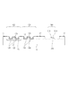
(第一の実施形態)
第一の実施形態に係る半導体装置について、図1を用いて説明する。図1は本実施形態の半導体装置の一部である集積構造を示す断面図である。図1に示した集積構造のトランジスタやショットキーバリアダイオードなどに、標準的なCMOSプロセスの後工程によって金属配線を接続すれば、本実施形態の半導体装置を得ることができる。半導体装置の構成、及び、詳細な製造方法については、後述する。
(First embodiment)
The semiconductor device according to the first embodiment will be described with reference to FIG. FIG. 1 is a cross-sectional view showing an integrated structure which is a part of the semiconductor device of this embodiment. The semiconductor device of this embodiment can be obtained by connecting a metal wiring to the integrated structure transistor, Schottky barrier diode, or the like shown in FIG. The configuration of the semiconductor device and the detailed manufacturing method will be described later.
本実施形態の半導体装置は、検出素子101と、p型MOSトランジスタ(以下、pMOSと呼ぶ)102と、n型MOSトランジスタ(以下、nMOSと呼ぶ)103と、を有する。これらの構成は、シリコン基板11(Si基板、以下、「基板11」と呼ぶ)上の面内方向に並んで配置されている。
The semiconductor device of this embodiment includes a
本実施形態のCMOSは、シリコン基板上(基板11上)のpMOS102とnMOS103などによって構成され、画像形成装置として基板11上に二次元状に多数並んでいるショットキーバリアダイオードアレイの制御及び信号処理に用いられる。
The CMOS according to the present embodiment includes a
ここでpMOS102、nMOS103は、標準的なCMOSプロセスを用いて製造されたものである。標準的なCMOSプロセスにはいくつかバリエーションがあり、本実施形態は、LOCOS(Local Oxidation of Si)法のn−wellプロセスにおける一例となっている。すなわち、図1の12は素子分離のためのフィールド酸化膜(局所熱酸化膜)、13はn型井戸領域(n−well)を示す。
Here, the
pMOS102及びnMOS103は、それぞれ、ソース(Source)及びドレイン(Drain)と、熱酸化膜(ゲート酸化膜)122、132と、ゲート(Gate)としてのポリシリコン123、133と、を有する。ソース及びドレインは、不純物拡散層121、131を含む。pMOS102とnMOS103との間、及びnMOS103と検出素子101との間には、それぞれ局所熱酸化膜12が設けられており、各素子を分離している。
Each of the
検出素子101は、基板11上に構成されテラヘルツ波を検出するためのもので、ショットキーバリアダイオードを有する。検出素子101は、陽極(anode)113と陰極(cathode)114との2つの電極と、エピタキシャル層112と、を有する。エピタキシャル層112の最表面にショットキー金属としての陽極113と陰極114とを付加することで、ショットキー障壁が形成されている。
The
エピタキシャル層112は、pMOS102のソース(Source)又はドレイン(Drain)における不純物拡散層121と組成及び高さが等しい不純物拡散層111の直上に、エピタキシャル成長によって形成される半導体層である。エピタキシャル層112は、単層に限らず、複数のレイヤを積層してもよい。
The
ここで、本明細書において、基板11上の組成及び高さが等しい層は、基板11上の場所及び目的は異なるものの、CMOSプロセスにおいて同一の工程を経て同時に形成される。なお、本明細書の「同時に形成」とは、各層が形成されたタイミングが完全に同じでなくてもよい。すなわち、半導体装置を形成において、同一の工程を行うことによって組成及び高さが等しくなった層については、組成及び高さが等しい層とみなすことができる。すなわち、本実施形態は、pMOS102におけるソース又はドレインの形成を目的として形成された不純物拡散層121又は131、と同時に形成された不純物拡散層111を、ダイオードの集積のためのシード層として用いたものである。その結果として、不純物拡散層の組成は基板11上の面内分布の範囲で等しく、面内方向における高さは同一の熱酸化工程及びエッチング工程で制御可能なスケールの範囲で等しい。この場合、エッチングの方が支配的で、高さが同一といっても典型的には数ナノメートルの表面ラフネスがある。
Here, in this specification, layers having the same composition and height on the
エピタキシャル成長の際、周囲の構造には、基板11及びポリシリコン123、133などのシリコンと、局所熱酸化膜12、熱酸化膜であるゲート酸化膜122、132などのガラスのみが存在する格好となる。これらの融点は、エピタキシャル成長における熱処理の温度と比較しても高いので、エピタキシャル成長の際の周囲の構造は熱処理に対する耐性を持つ。それゆえ、本実施形態の半導体装置は、標準的なCMOSプロセスにおける前工程を用いて形成でき、CMOS−コンパチブルな半導体装置であると言える。
At the time of epitaxial growth, the surrounding structure includes only silicon such as the
このようにして形成されるエピタキシャル層112は、もちろん不純物拡散層111に格子整合するSiでもよいが、別の材料でもよい。例えば、よく知られた技術を用いて、格子定数5.430ÅのSi基板11上に格子定数5.653ÅのGaAsの結晶を成長させることは実施可能である。また、格子不整合系のSiGeやGe、SiGe緩衝層を介したGaAsでもよい。エピタキシャル層112に含まれる材料の格子定数が5.430Å以上5.653Å以下であれば、Si基板11上に良質なエピタキシャル層112を形成できるため、この範囲内であることが好ましい。
The
また、エピタキシャル成長では、シード層である不純物拡散層111とその他の部分の格子定数やその他の性質、構造の違いによって基板11上のどの場所に成長するかを選択できる。非成長領域にはマスク材を用いて選択性を持たせることが可能であり、局所的に不純物拡散層111の直上にエピタキシャル層112を残すことも可能である。この際、成長条件(例えば、基板温度、原料比、圧力など)を調整すると選択性を高められる。
In addition, in epitaxial growth, it is possible to select a location on the
エピタキシャル成長の結晶成長方法は、CVD法(Chemical Vapor Deposition、化学気相成長法)や、MOVPE法(Metal−OrganicVapor Phase Epitaxy、有機金属気相成長法)が選択できる。CVD法、MOVPE法では、エピタキシャル層に微量の不純物が混入する可能性があるため、より不純物の少ないMBE法(Molecular Beam Epitaxy、分子線エピタキシー法)などを用いてもよい。いずれにしても、このエピタキシャル成長により、前工程で形成した素子に熱などによる影響がないような条件を選択できる。 As a crystal growth method for epitaxial growth, a CVD method (Chemical Vapor Deposition) or a MOVPE method (Metal-Organic Vapor Phase Epitaxy, metal organic vapor phase growth method) can be selected. In the CVD method and the MOVPE method, a trace amount of impurities may be mixed into the epitaxial layer, and therefore, an MBE method (Molecular Beam Epitaxy, molecular beam epitaxy method) with less impurities may be used. In any case, it is possible to select conditions under which the element formed in the previous step is not affected by heat or the like due to this epitaxial growth.
エピタキシャル成長の後、エピタキシャル層112の上に、陽極113と陰極114としてショットキー電極やオーミック電極を付加すると、ダイオード構造が完成する。好ましくは、エピタキシャル層112の最表層の上に、電極を配置する。
After the epitaxial growth, when a Schottky electrode or an ohmic electrode is added as the
本実施形態では、エピタキシャル層112は、シード層としての不純物拡散層111よりも小さな面積で残されている。これは、ダイオードにおけるテラヘルツ波の電気遅延を低減するためである。また、ダイオードは表面二電極型である。検出電流は、ダイオードの表面の陽極と陰極の付近を流れることになる。それゆえ、エピタキシャル層112の底部に多い不完全な格子構造の部分を検出電流が流れにくい構造となっているため、雑音が小さく、好ましい。
In this embodiment, the
また、標準的なCMOSプロセスにおける前工程を用いて形成する結果、局所熱酸化膜12は、検出素子101とpMOS102及びnMOS103との間に必ず位置し、面内方向の素子分離構造となる。さらに、本実施形態では、不純物拡散層111はp型半導体であるから、エピタキシャル層112にSiを選択した場合、導電型としてp型の反対のn型を選択すると、pMOS102、nMOS103やSi基板11などとの素子分離が可能になる。
Further, as a result of forming using a pre-process in a standard CMOS process, the local
シード層としての不純物拡散層111は、pMOS102のソース又はドレインにおける不純物拡散層121に限らず、nMOS103のソース又はドレインにおける不純物拡散層131と組成及び高さが等しいn型半導体を使用する変形例も考えられる。その場合は、エピタキシャル層として、p型半導体を成長した後にn型半導体を成長させた構造を用いても、同様の素子分離が可能である。イオン注入を用いて同様の構造を形成してもよい。
The
本実施形態の半導体装置は、CMOS−コンパチブルで、且つ、ショットキー障壁の特性を設計可能である。 The semiconductor device of this embodiment is CMOS-compatible and can be designed with Schottky barrier characteristics.
本実施形態の構成は、シード層111の露出工程が比較的容易でかつ構造も単純である一例である。本実施形態においては、不純物拡散層121形成と同一工程で同時に形成された不純物拡散層111の直上にエピタキシャル層112を成長している。不純物拡散層111、121、131は、いずれも基板11表面にイオン注入と活性化アニールを行うことで形成される。したがって、エピタキシャル成長前の不純物拡散層111は、前工程で用いている基板11の一部であり、基板11表面にエピタキシャル層112は形成される。しかし、エピタキシャル成長した半導体層(エピタキシャル層)112は、基板11の表面と同じ半導体種であった場合でも、その成長方法や条件によって、その不純物濃度、欠陥密度等の膜質が実質的に異なる物性を持つものとなる。
The configuration of this embodiment is an example in which the exposure process of the
すなわち、基板11表面は、CZ法(Czochralski法)、FZ法(Float Zone technology法)等の基板形成方法による物性を踏襲するものとなる。それに対し、エピタキシャル層112は、CVD法、MOVPE法であれば原料ガスに含まれるカーボン等の不純物が、MBE法においてはチャンバーの真空中に残留する不純物等が混入するものとなる。
That is, the surface of the
したがって、不純物拡散層121と組成及び高さが等しい層、すなわち不純物拡散層111上に成長した半導体層(エピタキシャル層)112と基板11の半導体層とは、分析及び電気的特性により区別できるものとなる。また、多くの場合、局所的にエピタキシャル成長をした場合には、エピタキシャル層112とシード層(不純物拡散層)111との界面に酸素等の不純物やアモルファス層が存在する場合がある。このように、本発明の製造方法で作製した素子は、その製造方法特有の構造を有するものとなる。
Therefore, a layer having the same composition and height as the
(第二の実施形態)
第二の実施形態に係る半導体装置について、図2を用いて説明する。図2は、本実施形態の半導体装置の一部である集積構造を示す断面図を表す。図2に示した半導体装置の集積構造に含まれるトランジスタやダイオードなどに、標準的なCMOSプロセスの後工程によって金属配線を接続すれば、本実施形態の半導体装置を得ることができる。なお、半導体装置の構成及び製造方法については、後述する。第一の実施形態と同一の部分については、説明を省略する。
(Second embodiment)
A semiconductor device according to the second embodiment will be described with reference to FIG. FIG. 2 is a cross-sectional view showing an integrated structure which is a part of the semiconductor device of this embodiment. The semiconductor device of this embodiment can be obtained by connecting a metal wiring to a transistor, a diode, or the like included in the integrated structure of the semiconductor device shown in FIG. 2 by a post process of a standard CMOS process. Note that the configuration and manufacturing method of the semiconductor device will be described later. Description of the same parts as those of the first embodiment is omitted.
本実施形態の半導体装置は、検出素子201と、pMOS102と、nMOS103と、を有する。本実施形態において、検出素子201は、第一の実施形態と同様に、Si基板11上に構成され、ミリ波帯からテラヘルツ帯までの電磁波を検出するための検出素子である。検出素子201は、陽極(anode)213と陰極(cathode)214との2つの電極と、エピタキシャル層212と、を有する。エピタキシャル層212の最表面にショットキー金属としての陽極213と陰極214とを付加することで、ショットキー障壁が形成されている。
The semiconductor device of this embodiment includes a
エピタキシャル層212は、本実施形態の場合、nMOS103のゲート酸化膜132の直下におけるシリコン基板中(基板11中)のチャネル領域と組成及び高さが等しい基板11中の領域の表面に、エピタキシャル成長によって設けられる。エピタキシャル層212を形成する領域は、pMOS102のゲート酸化膜122の直下における基板11中のチャネル領域と組成及び高さが等しい基板11中の領域の直上でもよい。なお、エピタキシャル層212は、単層に限らず、複数のレイヤを積層してもよい。
In this embodiment, the
本実施形態の組成及び高さが等しい領域とは、基板11上の場所及び目的は異なるものの、CMOSプロセスにおいて同一の工程を経て同時に形成されることを指す。その結果として、ゲート酸化膜132の直下における基板11中のチャネル領域の組成と図2においてはすでに除去されているゲート酸化膜の直下における基板11中のチャネル領域の組成とは、基板11上の面内分布の範囲で等しく、面内方向における高さは、同一の熱酸化工程で制御可能なスケールの範囲で等しい。なお、ゲートに関する熱酸化工程は非常に精密であり、典型的には1ナノメートル以下に制御可能である。
The region having the same composition and height in the present embodiment means that it is formed simultaneously through the same process in the CMOS process, although the location and purpose on the
本実施形態のSi基板11表面は、nMOSにおけるチャネル領域の形成を目的として形成された領域を、検出素子201の集積のためのシード層として用いたものである。したがって、ゲート熱酸化膜122、132と同一のプロセスを経た状態の基板11表面が成長のシード層になる。
The surface of the
第一の実施形態と同様に、成長の際、周囲の構造には、シリコンとガラスのみが存在する格好となる。これらの融点は非常に高いので、エピタキシャル成長における熱処理に対して耐性を持つ。そのため、図2に示す集積構造を用いた半導体装置も、標準的なCMOSプロセスを用いて形成できる、すなわち標準的なCMOSプロセスと親和性をもつCMOS−コンパチブルな半導体装置であると言える。 As in the first embodiment, during the growth, only the silicon and glass are present in the surrounding structure. Since these melting points are very high, they are resistant to heat treatment in epitaxial growth. Therefore, it can be said that the semiconductor device using the integrated structure shown in FIG. 2 can also be formed using a standard CMOS process, that is, a CMOS-compatible semiconductor device having an affinity with the standard CMOS process.
その結果、局所熱酸化膜12は検出素子201とpMOS102及びnMOS103の間に位置し、面内方向の素子分離構造となる。さらに、図2ではSi基板11はp型半導体であるから、エピタキシャル層212にSiを選択した場合、導電型としてp型と反対のn型を選択すると、pMOS102及びnMOS103、Si基板11などとの素子分離が可能になる。シード層としてのSi基板11としてpMOSにおけるn−wellを使用する変形例も考えられ、その場合は、エピタキシャル層にp型半導体を成長した後にn型半導体を成長してエピタキシャル層212を形成しても、同様の素子分離が可能である。
As a result, the local
本実施形態の構成は、エピタキシャル成長におけるシード層として、nMOS又はpMOSのゲート酸化膜の直下における基板中のチャネル領域と組成及び高さが等しい基板中の領域を用いている。このシード層は、欠陥などの少ない最良の表面状態が得られる構成であるが、ポリシリコンゲートとゲート熱酸化膜を除去する必要があることから、露出工程が比較的難しい構造の一例でいる。 In the configuration of this embodiment, a region in the substrate having the same composition and height as the channel region in the substrate immediately below the gate oxide film of nMOS or pMOS is used as the seed layer in the epitaxial growth. This seed layer is configured to obtain the best surface state with few defects and the like, but is an example of a structure in which the exposure process is relatively difficult because it is necessary to remove the polysilicon gate and the gate thermal oxide film.
露出工程では、リソグラフィによるパターニングなどによって、例えば、対象とするnMOSにおけるポリシリコンゲート(不図示)を除く部分をマスキングした後、ウェットエッチングを用いてポリシリコン(不図示)及び直下の熱酸化膜を除去する。エッチャントとしては、低濃度不純物ドープ単結晶シリコンによってエッチングが制止するフッ化水素酸と硝酸を含む混合溶液を用いることもできる。その際、ゲート側壁絶縁膜215をサイドエッチングの制止構造として用いてもよい。ただし、ゲート側壁絶縁膜215は、本構成にとって不要であるため、その後、除去してもよい。
In the exposure process, for example, after masking a portion of the target nMOS except for the polysilicon gate (not shown) by patterning by lithography, the polysilicon (not shown) and the thermal oxide film immediately below are removed by wet etching. Remove. As the etchant, a mixed solution containing hydrofluoric acid and nitric acid whose etching is stopped by low-concentration impurity-doped single crystal silicon can also be used. At that time, the gate sidewall insulating
なお、これを用いた画像形成装置については、CMOSプロセスの後工程を経た図5の構成と同様であり、詳細な説明は後述する。本実施形態においては、ゲート酸化膜132の直下の基板11中のチャネル領域と同一工程を経て同時に形成されたSi基板11中の領域の直上にエピタキシャル層212を成長している。したがって、エピタキシャル成長を行った領域は、チャネル領域で、前工程で用いている基板11の一部で表面である。
The image forming apparatus using this is the same as the configuration of FIG. 5 after the CMOS process, and will be described in detail later. In the present embodiment, the
第一の実施形態と同様に、エピタキシャル成長によって形成した半導体層(エピタキシャル層)122は、基板11表面と同じ半導体種を用いた場合でも、その成長方法や条件によって、不純物濃度、欠陥密度等の膜質は、実質的に異なる物性を持つものとなる。
Similar to the first embodiment, the semiconductor layer (epitaxial layer) 122 formed by epitaxial growth has a film quality such as impurity concentration and defect density depending on the growth method and conditions even when the same semiconductor species as the surface of the
本実施形態の半導体装置は、CMOS−コンパチブルで、且つ、ショットキー障壁の特性を設計可能である。 The semiconductor device of this embodiment is CMOS-compatible and can be designed with Schottky barrier characteristics.
(第三の実施形態)
第三の実施形態に係る半導体装置について、図3を用いて説明する。図3は、本実施形態の半導体装置の集積構造の一部を示す断面図である。図3に示した半導体装置の集積構造に含まれるトランジスタやダイオードなどに、標準的なCMOSプロセスの後工程によって金属配線を接続すれば、本実施形態の半導体装置を得ることができる。なお、半導体装置の構成及び製造方法については、後述する。上述の実施形態と同一の部分については、説明を省略する。
(Third embodiment)
A semiconductor device according to the third embodiment will be described with reference to FIG. FIG. 3 is a cross-sectional view showing a part of the integrated structure of the semiconductor device of this embodiment. The semiconductor device of this embodiment can be obtained by connecting the metal wiring to the transistors and diodes included in the integrated structure of the semiconductor device shown in FIG. Note that the configuration and manufacturing method of the semiconductor device will be described later. The description of the same parts as those in the above embodiment is omitted.
本実施形態の半導体装置は、検出素子301と、pMOS102と、nMOS103と、を有する。本実施形態において、検出素子301は、第一の実施形態と同様に、Si基板11上に構成され、ミリ波帯からテラヘルツ帯までの電磁波を検出するための検出素子である。検出素子301は、陽極(anode)313と陰極(cathode)314との2つの電極と、エピタキシャル層312と、を有する。エピタキシャル層312の最表面にショットキー金属としての陽極313と陰極314とを付加することで、ショットキー障壁が形成されている。 本実施形態において、検出素子301は、第一の実施形態と同様に基板11上に構成され、ミリ波帯からテラヘルツ帯までの電磁波を検出する検出素子である。エピタキシャル層312は、本実施形態の場合、pMOS102とnMOS103との間に形成された素子分離用の酸化膜12の直下の基板11の領域と組成及び高さが等しい基板11中の領域の直上にエピタキシャル成長によって形成される。なお、エピタキシャル層312は、単層に限らず、複数のレイヤを積層してもよい。
The semiconductor device of this embodiment includes a
本実施形態でも、組成及び高さが等しい領域とは、基板上の場所及び目的は異なるもののCMOSプロセスにおいて同一の工程を経て同時に形成されることを指す。その結果として、素子分離用の酸化膜12の直下の基板11の領域の組成は基板11上の面内分布の範囲で等しく、面内方向における高さは、熱酸化工程(LOCOS法)又はエッチング工程(溝型分離法)で制御可能なスケールの範囲で等しい。いずれにせよ、この場合、数ナノメートルの表面ラフネスは避けられない。こうした工程を経た結果、不純物が基板11に混ざるので最表層の組成は基板11の中の部分とはわずかに異なる。
Also in this embodiment, the region having the same composition and height means that the same process is performed through the same process in the CMOS process, although the location and purpose on the substrate are different. As a result, the composition of the region of the
本実施形態の基板11表面は、素子分離を行うための局所熱酸化膜12の直下の領域を、検出素子301の集積のためのシード層として用いたものである。したがって、局所熱酸化膜12を取り除いて露出した基板11表面がエピタキシャル成長のシード層になる。
The surface of the
第一の実施形態と同様に、成長の際、周囲の構造には、シリコンと、ガラスのみが存在する格好となる。これらの融点は非常に高いので、エピタキシャル成長における熱処理に耐性を持つ。それゆえ、図3に示す集積構造を用いた半導体装置も、標準的なCMOSプロセスにおける前工程を用いて形成可能で、標準的なCMOSプロセスと親和性をもつCMOS−コンパチブルな半導体装置であると言える。 As in the first embodiment, during the growth, only the silicon and glass are present in the surrounding structure. Since these melting points are very high, they are resistant to heat treatment in epitaxial growth. Therefore, the semiconductor device using the integrated structure shown in FIG. 3 can also be formed using the previous process in the standard CMOS process, and is a CMOS-compatible semiconductor device having an affinity with the standard CMOS process. I can say that.
その結果、局所熱酸化膜12は、検出素子301とpMOS102及びnMOS103の間に位置し、面内方向の素子分離構造となる。さらに、本実施形態でも、基板11はp型半導体であるから、エピタキシャル層312にSiを選択した場合、導電型としてp型と反対のn型を選択すると、pMOS102及びnMOS103、基板11などとの素子分離が可能になる。シード層としての基板11としてpMOS102におけるn−wellを使用する変形例も考えられ、その場合は、エピタキシャル層312として、p型半導体を成長した後にn型半導体を成長した構成を用いても同様の素子分離が可能である。
As a result, the local
本実施形態の構成は、エピタキシャル成長におけるシード層として、pMOS102とnMOS103との間に形成された素子分離用の酸化膜12の直下の基板11の領域と組成及び高さが等しい基板11中の領域を用いる。この場合、欠陥などの少ない表面状態の良いものが得られるが、第二の実施形態ほどではない。酸化膜12を取り除いてシード層としてのSi基板11表面を露出させる露出工程が比較的容易でかつ構造も単純であるが、第一の実施形態ほどではない。
In the configuration of this embodiment, a region in the
しかし、上述の実施形態と比較すると、基板11上の検出素子301の面積を節約できる。これは、比較的面積が大きくなりやすいLOCOS法による局所熱酸化膜12の一部を、検出素子301の形成領域として兼ねて使用することによる。ゆえに、本実施形態は、画素の精細化にとって都合が良い。
However, compared with the above-described embodiment, the area of the
なお、これを用いた半導体装置については、CMOSプロセスの後工程を経た後述する図5と同様の構成であるので、説明は省略する。 Note that a semiconductor device using the same has the same configuration as that of FIG.
本実施形態においては、pMOS102とnMOS103との間に設けられた素子分離用の酸化膜12の直下の基板11表面の形成と同時に形成されたSi基板11上の検出素子301を配置すべき領域の表面の直上にエピタキシャル層312を成長させる。したがって、エピタキシャル成長前の当該表面は前工程で用いている基板表面である。また、エピタキシャル成長した半導体層はその成長方法や条件によって、不純物濃度、欠陥密度等の膜質は前記基板表面とは同じ半導体種であっても実質的に異なる物性をもつものとなる。
In this embodiment, the region where the
本実施形態の半導体装置は、CMOS−コンパチブルで、且つ、ショットキー障壁の特性を設計可能である。 The semiconductor device of this embodiment is CMOS-compatible and can be designed with Schottky barrier characteristics.
(第四の実施形態)
第四の実施形態に係る半導体装置について、図4を用いて説明する。図4は、本実施形態の半導体装置の集積構造の一部を示す断面図である。図4に示した半導体装置の集積構造に含まれるトランジスタやMESFETなどに、標準的なCMOSプロセスの後工程によって金属配線を接続すれば、本実施形態の半導体装置を得ることができる。本実施形態の半導体装置の構成及び製造方法については、後述する。上述の実施形態と同一の構成については、説明を省略する。
(Fourth embodiment)
A semiconductor device according to the fourth embodiment will be described with reference to FIG. FIG. 4 is a cross-sectional view showing a part of the integrated structure of the semiconductor device of this embodiment. The semiconductor device of this embodiment can be obtained by connecting the metal wiring to the transistors, MESFETs, and the like included in the integrated structure of the semiconductor device shown in FIG. The configuration and manufacturing method of the semiconductor device of this embodiment will be described later. The description of the same configuration as that of the above-described embodiment is omitted.
本実施形態の半導体装置は、検出素子401と、pMOS402と、nMOS403と、を有する。本実施形態において、検出素子401は、テラヘルツ波を検出するMESFETである。検出素子401は、ソース(Source)413、ゲート(Gate)416及びドレイン(Drain)414の3つの電極と、エピタキシャル層412と、を有し、ショットキー障壁を形成している。エピタキシャル層412は半導体層で、単層に限らず、複数のレイヤを積層してもよい。ショットキーバリアダイオードの場合、ショットキー障壁は、n型半導体を伴った陽極直下又はp型半導体を伴った陰極直下に設けるのが典型的であるが、MESFETの場合、ゲート直下にショットキー障壁を設ける。
The semiconductor device of the present embodiment includes a
CMOSは、シリコン基板41(以下、「基板41」と呼ぶ)上のpMOS402とnMOS403などを含み構成され、画像形成装置としてSi基板41上の面内方向に多数並んでいるMESFETアレイの制御及び信号処理に用いられる。
The CMOS includes a
ここで、pMOS402及びnMOS403は標準的なCMOSプロセスを用いて製造されたものである。本実施形態は、溝型分離法のtwin−wellプロセスにおける一例となっている。すなわち、半導体装置は、素子分離のためのフィールド酸化膜(CVD酸化膜)42、n型井戸領域(n−well)43、及び、p型井戸領域(p−well)44を有する。基板41の導電型は、p型、n型不問となる。
Here, the
pMOS402とnMOS403はそれぞれ、ソース(Source)及びドレイン(Drain)としての不純物拡散層421、431と、熱酸化膜(ゲート酸化膜)422、432と、ゲート(Gate)としてのポリシリコン423、433と、を有する。pMOS402とnMOS403と検出素子401との間には、CVD法で形成した酸化膜42が設けられており、各素子を分離している。
The
溝型分離法を用いた本実施形態でも、第一の実施形態と同様にエピタキシャル層412は、pMOS402のソース又はドレインにおける不純物拡散層421と組成及び高さが等しい不純物拡散層411の直上にエピタキシャル成長によって形成されている。あるいは、nMOS403のソース又はドレインにおける不純物拡散層431と組成及び高さが等しい不純物拡散層411の直上にエピタキシャル層412を成長してもよい。
Also in this embodiment using the trench type isolation method, the
第一の実施形態でも説明したように、エピタキシャル層412がSiの場合、エピタキシャル層412が不純物拡散層411の導電型とは異なる導電型のレイヤを含むと、素子分離が行える。エピタキシャル層412としてSiGeを用いた場合でも同様である。
As described in the first embodiment, when the
エピタキシャル層412がGaAsやInPの場合は、これらよりバンドギャップが大きな材料、たとえばAlGaAs(アルミニウムガリウムヒ素)やInGaAs(インジウムガリウムヒ素)などを採用すれば素子分離が容易である。III−V化合物半導体では、深い不純物の導入などによってキヤリアを補償して抵抗率を高抵抗化する技術が進んでおり、バンドギャップが大きな材料を用いなくても素子分離は可能である。
In the case where the
溝型分離法において第二の実施形態のような構成も考えられる。すなわち、エピタキシャル層412は、pMOS402又はnMOS403のゲート熱酸化膜422又は432の直下における基板41中のチャネル領域と組成及び高さが等しい基板41中の領域の表面にエピタキシャル成長してもよい。第二の実施形態と同様に、エピタキシャル成長におけるシード層41として、欠陥などの少ない良い表面状態が得られる構成である。
In the groove type separation method, a configuration as in the second embodiment is also conceivable. That is, the
また、第三の実施形態のように、酸化膜42の直下における基板41中の領域と組成及び高さが等しい基板41中の領域の表面にエピタキシャル層412を成長してもよい。Si基板41表面としては、p−well43上を選んでもよいし、n−well44上を選んでもよい。この場合、第三の実施形態と同様に、酸化膜42をMESFET401の形成領域として兼ねて使用できるため、画素の精細化にとって都合が良い。
Further, as in the third embodiment, the
溝型分離法を用いた標準的なCMOSプロセスにおいても、LOCOS法と同じように、エピタキシャル成長の際、周囲の構造には、シリコンと、CVD酸化膜42、熱酸化膜422、432などのガラスが存在する格好となる。
In the standard CMOS process using the trench type separation method, as in the LOCOS method, silicon and a glass such as the
さらに、本実施形態のCMOSプロセスで形成されたpMOS402及びnMOS403それぞれのソース及びゲート、ドレインに、後工程に用いる金属との接触における接触抵抗低減のためのシリサイド424、434を伴っている。これは、Siと金属の混晶の化合物であって、例えば、WSi(タングステンシリサイド)、TiSi(チタニウムシリサイド)、CoSi(コバルトシリサイド)、NiSi(ニッケルシリサイド)などが典型的である。これらの融点は、エピタキシャル成長における熱処理と比較しても非常に高い。
Furthermore,
すなわち、本実施形態の標準的なCMOSプロセスの前工程を用いて形成された各構造は、エピタキシャル成長のための熱処理対する耐性及び物理的安定性を持つ。それゆえ、本実施形態の半導体装置は、CMOS−コンパチブルで、且つ、ショットキー障壁の特性を設計可能である。 That is, each structure formed using the pre-process of the standard CMOS process of the present embodiment has resistance and physical stability against heat treatment for epitaxial growth. Therefore, the semiconductor device of this embodiment is CMOS-compatible and can be designed with Schottky barrier characteristics.
本実施形態では、エピタキシャル成長の後に、当該エピタキシャル層の上にゲート電極416及びソース電極413、ドレイン電極414を付加すると、MESFET401構造は完成する。好ましくはエピタキシャル層412の最表層の上に、ゲート電極を配置する。
In this embodiment, the
なお、これを用いた画像形成装置については、標準的なCMOSプロセスの後工程を経た次の図5と同様の構成であるので、説明は省略する。 The image forming apparatus using this has the same configuration as that shown in FIG. 5 after the standard CMOS process and will not be described.
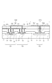
(第五の実施形態)
第五の実施形態に係る半導体装置について、図5を用いて説明する。図5は、本実施形態の半導体装置の一部を示す断面図である。具体的には、第一の実施形態に係る半導体装置の一部である集積構造に標準的なCMOSプロセスにおける後工程を実施し、検出素子と検出信号の制御、信号処理を行う回路を少なくとも含む一画素を説明するものである。上述の実施形態と同一の構成については、説明を省略する。
(Fifth embodiment)
A semiconductor device according to a fifth embodiment will be described with reference to FIG. FIG. 5 is a cross-sectional view showing a part of the semiconductor device of this embodiment. Specifically, the integrated structure that is a part of the semiconductor device according to the first embodiment includes at least a circuit that performs a post-process in a standard CMOS process, controls a detection element, a detection signal, and performs signal processing. One pixel will be described. The description of the same configuration as that of the above-described embodiment is omitted.
本実施形態の半導体装置は、検出回路1001(以下、「回路1001」と呼ぶ)と、制御・信号処理回路1002(以下、「回路1002」と呼ぶ)と、を有する。
The semiconductor device of this embodiment includes a detection circuit 1001 (hereinafter referred to as “
回路1001は、テラヘルツ波の検出を行う部分で、検出素子101と、金属要素1621、1622で形成されたアンテナと、を有する。検出素子101とアンテナ1621、1622とは、ビア151、161及び電極113、114を介して電気的に接続されている。
The
ここでアンテナ1621、1622は、自由空間を伝搬するテラヘルツ波を捕え、検出素子101のショットキーバリアダイオードのインピーダンスに近い電流と電圧に変換する働きを持つ。本実施形態のアンテナ1621、1622は、平面アンテナのパターンを、第二の金属配線162によって形成している。もちろん第一の金属配線152と第二の金属配線162を用いた金属二層を用いたアンテナでもよい。
Here, the
ビア151、161は金属で、アンテナ1621、1622からの高周波電気信号を低損失で検出素子101へ伝える働きを持つ。検出素子101は、高周波電気信号を整流するなどしてアンテナ1621、1622が受信したテラヘルツ波の強度に比例した検出信号を生成する働きを持つ。検出信号は、第一の層間絶縁膜15上の第一の金属配線152、もしくは第二の層間絶縁膜16上の第二の金属配線162を通じて、回路1002へ取り出される。
The vias 151 and 161 are made of metal and have a function of transmitting high-frequency electric signals from the
回路1002は、増幅回路で、pMOS102とnMOS103とを、ビア151、161及び第一の金属配線152、第二の金属配線162を介して電気的に接続して構成される。さらに、第三、第四の金属配線を用いてもよい。本実施形態では、pMOS102とnMOS103とを接続した回路1002のCMOS部分のみの断面構造を示しているが、基板11上の抵抗素子、容量素子などを伴って増幅回路を構成することが出来る。こうした回路構成は、回路1001からの電気信号を増幅するために使用してもよい。
The
また、回路1002は、外部回路からの命令で信号出力を停止することもできるため、画素スイッチとしての役割を持たせることも可能である。ゆえに、一ライン100画素のような大規模な画素数を有する撮像素子において、任意の画素へのアクセス・アドレスのための制御に使用してもよい。こうした理由により、回路1002は本実施形態に係る半導体装置に欠かせない。
In addition, since the
図5に示したように、本実施形態の半導体装置は、同一基板11上の隣接した場所に回路1001と回路1002とが集積されている。通常、回路1001からの検出信号に外来の雑音が重複しやすく、回路1001と回路1002との接続配線が長い程顕著である。したがって、回路1001と回路1002とを最短で接続することが出来る本実施形態の構成は、検出信号のS/N比が優れるため好ましい。
As shown in FIG. 5, in the semiconductor device of this embodiment, a
例えば、サンプリング定理によれば画素の一辺の大きさは半波長が妥当であり、1THzでは画素の大きさは空気中で150μmとなる。隣接して集積された回路1001と回路1002とを半波長以下の長さで接続するのは容易であり、優れたS/Nのために好ましい。
For example, according to the sampling theorem, a half wavelength is appropriate for the size of one side of the pixel, and at 1 THz, the size of the pixel is 150 μm in the air. It is easy to connect adjacently integrated
さらに、外来の雑音を低減する様な構成も容易である。例えば、接続配線として第一の金属配線152の様な低階の配線を用いた場合、遮蔽板として第二の金属配線162の様な高階の配線を用いてもよい。遮蔽板としての第二の金属配線162と基板11との間を、ビア151、161を介して接続し、遮蔽効果を高めると効果的である。いずれにせよ、外来の雑音を遮蔽し低減できる構成は、同一基板11上に集積しなければ難しい。
Furthermore, a configuration that reduces external noise is easy. For example, when a lower floor wiring such as the
トランジスタや各種素子間に金属配線を接続する加工の際、周囲の構造には、熱処理が完了している検出素子101と、基板11及びポリシリコン123、133などのシリコンと、が存在する。また、CMOSプロセスの前工程で形成された局所熱酸化膜12及び熱酸化膜122、132などのガラスが存在する。標準的なCMOSプロセスにおける後工程では、こうした構造が経験した温度よりも低い温度の熱処理を伴う材料が採用される。
At the time of processing for connecting a metal wiring between a transistor and various elements, the surrounding structure includes a
例えば、層間絶縁膜15、16としてはプラズマCVD酸化窒化膜やTEOS(Tetra Ethyl Ortho Silicate)膜などが選択される。これらは熱酸化膜よりも十分に低温で成膜することが出来る。ビア151、161としては、CVD金属やメッキ金属が選択される。CVD−W法は、400℃前後の熱処理をもってビアをW(タングステン)で充填することが出来る。最近では、Cuダマシン法も選択することが可能で特別な熱処理を伴わずにビアをCuで充填することが出来る。
For example, a plasma CVD oxynitride film, a TEOS (Tetra Ethyl Ortho Silicate) film, or the like is selected as the
金属配線152、162としては、比較的安価でかつ導電率の高いAlや、デュアルダマシン法に対応したCuなどが選択される。それゆえ、本実施形態の半導体装置は、標準的なCMOSプロセスにおける後工程を適用できると言える。
As the
なお、用語の定義のため、標準的なCMOSプロセスにおける前工程の一例を、図6、図7を参照して説明する。図6は、LOCOS法における工程順の一例であり、図7は、溝型分離法における工程順の一例である。 For the definition of terms, an example of a pre-process in a standard CMOS process will be described with reference to FIGS. FIG. 6 shows an example of the process order in the LOCOS method, and FIG. 7 shows an example of the process order in the groove type separation method.
LOCOS法における工程は、図6における(a)から(k)までのプロセスを経る。まず、Si基板を用意し、基板表面上に分布する不純物の洗浄(図6(a))、ゲート熱酸化膜形成のための表面熱酸化(図6(b))、n−well形成のためのイオン注入と活性化アニール(図6(c))から始まる。その後、窒化膜(SiN)成膜(図6(d))、バーズビークのパターン形成を行うための窒化膜エッチング(図6(e))、LOCOS法の最大の特徴であるフィールド酸化膜(局所熱酸化膜、SiO)の形成(図6(f))を実施する。 The steps in the LOCOS method go through processes (a) to (k) in FIG. First, a Si substrate is prepared, and impurities distributed on the substrate surface are cleaned (FIG. 6A), surface thermal oxidation for forming a gate thermal oxide film (FIG. 6B), and n-well formation. First, ion implantation and activation annealing (FIG. 6C) are started. Thereafter, a nitride film (SiN) is formed (FIG. 6D), a nitride film etching for forming a bird's beak pattern (FIG. 6E), and a field oxide film (local heat) which is the greatest feature of the LOCOS method. An oxide film (SiO) is formed (FIG. 6F).
その後、必要に応じてpMOS、nMOSのしきい値電圧Vthを決めるためのイオン注入と活性化アニール(図6(g))を実施し、次にゲートとなる予定のポリシリコン成膜及びエッチングを行って図6(h)の工程が完了する。続いて、pMOS、nMOSのソース又はドレインとなる不純物拡散層を形成するためのイオン注入及び活性化アニールを行い、図6(i))に示した構成を形成する。さらに、ゲート側壁絶縁膜のCVD酸化膜(SiO)成膜(図6(j))、及び、ゲート側壁絶縁膜形成を兼ねたコンタクトの露出工程(図6(k))を経て、前工程は終了する。 Thereafter, ion implantation and activation annealing (FIG. 6 (g)) for determining the threshold voltage Vth of the pMOS and nMOS are performed if necessary, and then polysilicon film formation and etching to be the gate are performed. Then, the process of FIG. 6H is completed. Subsequently, ion implantation and activation annealing are performed to form an impurity diffusion layer serving as the source or drain of the pMOS and nMOS, thereby forming the configuration shown in FIG. Further, after the CVD oxide film (SiO) film formation (FIG. 6 (j)) of the gate sidewall insulating film and the contact exposure process (FIG. 6 (k)) also serving as the gate sidewall insulating film formation, finish.
溝型分離法における前工程は、図7における(a)から(l)までのプロセスを経る。まず、Si基板を用意し、基板表面上に分布する不純物の洗浄(図7(a))、基板表面保護の酸化膜成膜と窒化膜成膜(図7(b))、窒化膜をマスクとした溝パターンの形成を行うためのエッチング(図7(c))から始まる。その後、CVD酸化膜(SiO)等を成膜し、表面の平滑化のためのCMP(化学機械研磨)によって図7(d)の工程を行う。続いて、窒化膜(SiN)と酸化膜(SiO)エッチング(図7(e))によって、溝型分離法の最大の特徴である溝型の分離構造を、このトレンチにCVD酸化膜を充填する方法STI(Shallow Trench Isolation)で形成する。その後、n−well形成のためのイオン注入と活性化アニール(図7(f))を実施する。 The pre-process in the groove type separation method goes through processes (a) to (l) in FIG. First, an Si substrate is prepared, and impurities distributed on the substrate surface are cleaned (FIG. 7A), oxide film formation and nitride film formation for protecting the substrate surface (FIG. 7B), and the nitride film as a mask. It starts from etching (FIG. 7C) for forming the groove pattern. Thereafter, a CVD oxide film (SiO) or the like is formed, and the process of FIG. 7D is performed by CMP (chemical mechanical polishing) for smoothing the surface. Subsequently, the trench type isolation structure, which is the greatest feature of the trench type isolation method, is filled with a CVD oxide film in the trench by the nitride film (SiN) and the oxide film (SiO) etching (FIG. 7E). It forms with method STI (Shallow Trench Isolation). Thereafter, ion implantation for forming n-well and activation annealing (FIG. 7F) are performed.
必要に応じてさらに基板表面上の洗浄を行った後、表面熱酸化を行ってゲート熱酸化膜の形成(図7(g))、ゲートとなるポリシリコン成膜とエッチング(図7(h))を行う。続いて、pMOSのソース及びドレインとnMOSのソース及びドレインにおけるLDD(Lightly Doped Drain)構造を形成するためのイオン注入と活性化アニール(図7(i))を行う。さらに、ゲート側壁絶縁膜の形成(図7(j))、pMOSのソース及びドレインとnMOSのソース及びドレインとしての不純物拡散層を形成するためのイオン注入と活性化アニール(図7(k))を行う。続いて、コンタクトの改良のためにTi、Co、Niなどを接触させて熱処理を行うシリサイド化(図7(l))を経て、前工程は終了する。 After further cleaning on the substrate surface as necessary, surface thermal oxidation is performed to form a gate thermal oxide film (FIG. 7 (g)), polysilicon film formation and etching to be a gate (FIG. 7 (h)) )I do. Subsequently, ion implantation and activation annealing (FIG. 7 (i)) are performed to form an LDD (Lightly Doped Drain) structure in the source and drain of the pMOS and the source and drain of the nMOS. Further, formation of gate sidewall insulating films (FIG. 7 (j)), ion implantation and activation annealing for forming impurity diffusion layers as pMOS sources and drains and nMOS sources and drains (FIG. 7 (k)). I do. Subsequently, the silicidation (FIG. 7 (l)) in which Ti, Co, Ni, etc. are brought into contact with each other for heat treatment to improve the contact is completed.
なお、図7(l)は、しきい値電圧Vthを決めるためのイオン注入と活性化アニールや、LDD構造の形成工程やシリサイド化工程はCMOSのデザインルールの微細化に伴った機能性の向上のための工程であって必ずしも必須ではない。LOCOS法、溝型分離法、どちらの方法にもこうした工程を組み入れてもよい。例えば、図7(d)のCMP工程も同様に必須ではなく、旧来からよく知られるエッチバック法による表面の平滑化工程に置き換えてもよい。 In FIG. 7L, the ion implantation and activation annealing for determining the threshold voltage Vth, the LDD structure forming process, and the silicidation process are improved in functionality with the miniaturization of CMOS design rules. It is a process for, and is not necessarily essential. Such a process may be incorporated into either the LOCOS method or the groove type separation method. For example, the CMP process of FIG. 7D is not essential, and may be replaced with a surface smoothing process by an etch-back method that is well known from the past.
CMOSプロセスにおいて、この次に実施するPMD(Pre Metal Dielectric)形成工程は、本明細書における前工程に含んでも含まなくてもよい。これは、PMDの材料としては、典型的には、SiOやPGS(リンガラス)などが選択されるため、結果的にエピタキシャル成長の熱処理に対する耐性及び物理的安定性を持つからである。 In the CMOS process, a PMD (Pre Metal Dielectric) forming step to be performed next may or may not be included in the previous step in this specification. This is because, as a material for PMD, typically, SiO, PGS (phosphorus glass), or the like is selected, and as a result, it has resistance to heat treatment of epitaxial growth and physical stability.
また、CMOSプロセスの前工程における素子分離の手段のバリエーションを図8に示す。図8(a)は、p型のSi基板81(以下、「基板81」と呼ぶ)上にイオン注入法、拡散法などでn型井戸領域83を形成するn−wellプロセスを示している。図8(b)は、n型の基板81上にp型井戸領域84を形成するp−wellプロセスを示している。図8(c)は、基板81上に両導電型の井戸領域83、84を形成するtwin−wellプロセス、図8(d)は、p型の基板81上に基板と反対の導電型の井戸領域85と両導電型の井戸領域83、84とを形成するtriple−wellプロセスである。
FIG. 8 shows a variation of element isolation means in the previous process of the CMOS process. FIG. 8A shows an n-well process in which an n-
これらの組み合わせだけでも、標準的なCMOSプロセスであるLOCOS法及び溝型分離法の各々に8つのバリエーションがある。しかしながら、本明細書における標準的なCMOSプロセスはこれだけには限られない。 Even with these combinations alone, there are eight variations in each of the LOCOS method and the trench isolation method, which are standard CMOS processes. However, the standard CMOS process in this specification is not limited to this.
例えば、
・同一の構造を形成するための工程順に任意性がある場合、こうした工程順の組み換えを伴うCMOSプロセス
・同一の構造を形成するための工程に代替手段がある場合、こうした工程の置き換えを伴うCMOSプロセス
・機能性は向上するが必ずしも必須ではない構造を形成するための工程を追加あるいは省略するCMOSプロセス
・pMOS、nMOSとの同一基板上に不純物拡散層やポリシリコンを用いた抵抗素子、MOS型容量素子を形成するための工程が追加されているCMOSプロセス
・基板洗浄、表面処理など構造を伴わない工程を追加あるいは省略するCMOSプロセス
For example,
-CMOS process with recombination of these process orders if there is any order in the process order to form the same structure-CMOS with replacement of such processes if there are alternative means to the process to form the same structure Process-CMOS process that adds or omits steps to form a structure that improves functionality but is not necessarily required-Resistive element using impurity diffusion layer or polysilicon on the same substrate as pMOS and nMOS, MOS type CMOS process with additional steps for forming capacitive elements ・ CMOS process with additional or omitted steps without structure such as substrate cleaning and surface treatment
以上のCMOSプロセス及びそれらの組み合わせはすべて、本明細書おける標準的なCMOSプロセスとして考える。また、以上のCMOSプロセスを採用したバイポーラトランジスタとCMOSを集積するBiCMOSプロセスについても同様に考える。 All of the above CMOS processes and combinations thereof are considered as standard CMOS processes in this specification. The same applies to a BiCMOS process that integrates a bipolar transistor and a CMOS employing the above CMOS process.
このように、本実施形態の半導体装置は、CMOS−コンパチブルで、且つ、ショットキー障壁の特性を設計可能である。 Thus, the semiconductor device of this embodiment is CMOS-compatible and can be designed with Schottky barrier characteristics.
本実施例では、上述の実施形態の半導体装置を用いた撮像素子について、図9を用いて具体的に説明する。図9(a)は、本実施例に係る撮像素子の一部である半導体装置の断面図、図9(b)は、こうした構造を二次元アレイ状に配列して、任意の画素にアクセス可能な撮像素子の回路図を表すものである。半導体装置は、検出回路9001(以下、「回路9001」と呼ぶ)と、制御・信号処理回路9002(以下、「回路9002」と呼ぶ)と、を有する。
In this example, an image sensor using the semiconductor device of the above-described embodiment will be specifically described with reference to FIG. FIG. 9A is a cross-sectional view of a semiconductor device that is a part of the image sensor according to the present embodiment, and FIG. 9B is a two-dimensional array of such structures, which can access any pixel. 2 is a circuit diagram of a simple image sensor. The semiconductor device includes a detection circuit 9001 (hereinafter referred to as “
回路9001は、検出素子901と、金属要素9621、9622で形成されたアンテナと、を有する。検出素子901とアンテナ9621、9622とは、ビア951、961及び2つの電極913、914を介して電気的に接続されている。回路9002は、増幅回路で、pMOS902とnMOS903とを、ビア951、961及び第一の金属配線952、第二の金属配線962を介して電気的に接続して構成される。さらに、第三、第四の金属配線を用いてもよい。これらの構成は、第5の実施形態の半導体装置を同様のため、詳細な説明を省略する。
The
本実施例において、基板91は、200mm直径の8インチSi基板を用いる。8インチSi基板の採用によって、例えば、一画素0.6mm角、150×200画素数のダイ(半導体装置)を得ることができる。基板91は、抵抗率が20Ωcm以上のMCZ法の高抵抗率品を用いており、テラヘルツ波の基板91による吸収を低減している。
In this embodiment, the
検出素子901は、エピタキシャル層912と、ショットキー電極913と、オーミック電極914と、を有するショットキーバリアダイオード(以下、ダイオードと呼ぶ)である。エピタキシャル層912の最表面は、n型SiGe混晶半導体を用いる。エピタキシャル層912は、基板91側から順に高濃度ドープSi層(第一の層)9121と、高濃度ドープSi0.86Ge0.14層(第二の層)9122と、低濃度ドープSi0.86Ge0.14層(第三の層)9123と、を含み構成される。第一の層9121は、n型キャリア濃度が2×1019cm−3、厚さは500nmであり、第二の層9122は、n型キャリア濃度が2×1019cm−3、厚さは15nmである。第三の層9123は、n型キャリア濃度が5×1017cm−3、厚さは60nmである。
The
第一の層9121は、緩衝層を兼ねているため比較的厚めのレイヤを用いる。シード層の表面が完全ではない場合、エピタキシャル層912最下部が完全結晶になりにくいからである。なお、本実施例では、シード層として、pMOS902又はnMOS903のゲート酸化膜の直下の基板91中のチャネル領域と組成及び高さが等しい基板91中の領域を用いる。
Since the
第二の層9122及び第三の層9123は、基板91とは格子不整合系である。これらの層には低温エピタキシャル成長技術を用いると、転移、ミスフィットなどが低減できることが良く知られている。なお、第三の層9123におけるキャリア濃度に1×1017cm−3以上1×1019cm−3以下を選択するとショットキーバリア構造を形成するために好都合である。第三の層9123は、ショットキー電極913と接触して、エピタキシャル層912に含まれる半導体9123側にショットキーバリアを形成する。
The
オーミック電極914は、高濃度イオン注入領域9124を介して高濃度ドープ層9121、9122と電気的に接する。本実施例では、ショットキー電極913及びオーミック電極914の材料としてTi金属(厚さは200nm)を用いる。こうして、検出素子901を構成する。
The
図10は、SiGeエピタキシャル層912の低濃度ドープ層9123におけるGe混晶比、ショットキー電極913の材料を変化させたときのバリアポテンシャルの大きさについて示している。ショットキー電極913としてのTi、Al、Ni、Pdの成膜にはSiGeエピタキシャル層912の表面損傷を低減するために蒸着法を用いた。
FIG. 10 shows the magnitude of the barrier potential when the Ge mixed crystal ratio in the lightly doped
まず、ショットキー電極913の材料を変化させたときのバリアポテンシャルの大きさについて述べる。図10(a)及び図10(b)は、ショットキー障壁の高さ(Schottky Barrier Height)φbと電極に用いる金属の仕事関数(Metal Workfunction)との関係を示す図である。
First, the magnitude of the barrier potential when the material of the
ショットキー障壁の高さφbは、SiGeを含むエピタキシャル層912がp型半導体の場合、図10(a)の如く金属の仕事関数の増加とともに右下がりの特性となる。n型半導体の場合、図10(b)の如く金属の仕事関数の増加とともに右上がりの特性となった。これらのプロットにおいて、ショットキー障壁の高さφbの抽出にはI−V(電流−電圧)法を用いた。金属仕事関数の値は、WALTER H. KOHL著、“Materials and Techniques for ELECTRON TUBES”、p.526の表より抽出したものである。
When the
図10(c)は、SiGeを含むエピタキシャル層912におけるGeの混晶の程度と、ショットキー障壁の高さφb、間接的バンドギャップEgとの関係を表す図である。図10(c)は、Geの混晶の程度によって、ショットキー障壁の高さφbを調整できることも示している。同図は、とくにp型半導体の例を示しているが、SiGeはGe混晶比を増加させるとともに間接的バンドギャップEgが狭くなるため、その傾向に沿ってショットキー障壁の高さφbも減少する。
FIG. 10C is a diagram showing the relationship between the degree of mixed crystal of Ge in the
低雑音で高感度な検出が求められるテラヘルツ波の検出には、検出素子901のゼロバイアス動作(動作点が0V、0A)を実現することが一つの方法である。そのために、ショットキー障壁の高さφbは0.4eV以下、望ましくは0.1eV以上0.3eV以下が好ましい。それゆえ、p型半導体Si、SiGeにおいては、仕事関数が4.6eVのNiから仕事関数が5.0eVのPdまでのショットキー金属との組み合わせが好ましい。n型半導体Si、SiGeにおいては、仕事関数が3.9eVのTiから仕事関数が4.2eVのAlまでのショットキー金属との組み合わせが好ましい。
One method for detecting a terahertz wave that requires low-noise and high-sensitivity detection is to realize a zero bias operation (operating point is 0 V, 0 A) of the
本実施例では回路9001は、検出素子901とアンテナ9621、9622を接続して構成される。アンテナ9621、9622には、よく知られた周波数無依存の対数周期アンテナを用いる。
In this embodiment, the
本構成においては、検出素子901は島状に形成される。島の大きさは、0.5THz以上3THz以下の周波数帯の電磁波の検出のために50μm2程度かそれ以下とし、エピタキシャル層912の一辺を約7μmに設計した。エピタキシャル層912のシード層となるチャネルは一辺を約500μmと、ほぼ一画素と同じだけの大きさに設計した。
In this configuration, the
ダイオード構造における時定数、すなわち接合容量と直列抵抗の積を低減するため、ショットキー電極913の直径は0.6μm、ショットキー電極913とオーミック電極914との間の距離を1μmに設計した。ショットキー電極913及びオーミック電極914は、Tiを用いて形成したTi電極である。
In order to reduce the time constant in the diode structure, that is, the product of junction capacitance and series resistance, the diameter of the
Ti/Al/TiN配線952、962(厚さ800nm)は、それぞれ、BPSG膜95(最も厚い場所で厚さ2μm)、TEOS膜96(厚さ1.6μm)上に配置され、アンテナ9621、9622を形成する。直径0.4μmのCVD−Wで充填されるビア951、961は、それぞれ、Ti電極913、914と第一の配線952とを、第一の配線952と第二の配線962とを接続する。また、検出素子901とアンテナ9621、9622との間を直列抵抗4Ωで接続する。
Ti / Al / TiN wirings 952 and 962 (thickness 800 nm) are disposed on the BPSG film 95 (thickness 2 μm at the thickest location) and TEOS film 96 (thickness 1.6 μm), respectively, and
本実施例ではpMOS902、nMOS903は、LOCOS法のn−wellプロセスによって作製する。ソース、ドレイン、ゲートそれぞれの極においては、シリサイド924、934を採用している。本構成において、pMOS902、nMOS903はゲート面積が比較的大きくなるように形成される。CMOSにおける1/f雑音の低減のためである。
In this embodiment, the
そこで、pMOS902のゲート長は0.6μm、ゲート幅は240μm、nMOS903のゲート長は4.8μm、ゲート幅は8μmと設計した。このような長いゲート幅における寄生容量を低減するため、MOSを分割して、例えば、コモンセントロイド配置としてもよい。これらは周知の技術としてよく知られている。
Therefore, the gate length of the
Ti/Al/TiN配線952、962(厚さ800nm)は、それぞれ、BPSG膜95(最も厚い場所で厚さ2μm)、TEOS膜96(1.6μm)上に配置される。直径0.4μmのビア951、961は、それぞれ、pMOS902、nMOS903におけるソース及びドレイン及びゲートと第一の配線952とを、第一の配線952と第二の配線962とを比較的低抵抗で接続する。それにより、次に説明する回路9002を形成する。
Ti / Al / TiN wirings 952 and 962 (thickness 800 nm) are respectively disposed on the BPSG film 95 (thickness 2 μm in thickness) and TEOS film 96 (1.6 μm).
本実施形態の回路9002は、単純なソース接地回路を用いて設計したLNA回路である。例えば、pMOS902のソースとnMOS903のゲートへ1V、nMOS903のソースへ−1Vのバイアスを行えば、増幅度が20dB、帯域が10MHzのLNAとして動作する。帯域は比較的広いため、例えば、後段にフィルター回路などを設けて帯域制限すると低雑音となり好ましい。これらは周知の技術としてよく知られている。
The
本実施例では、検出素子901をゼロバイアス動作させるため、回路9001を回路9002の入力段に直接接続しているが、容量結合等を用いて非ゼロバイアス動作させる構成としても良い。入力段に保護用の抵抗などを挿入してももちろん良い。こうした回路構成は同一基板91上に容易に集積することが出来る。
In this embodiment, the
本実施例の撮像素子は、一画素に回路9001、回路9002を備えた構成で、これを二次元状にアレイ化している。そのため、指定する画素の読み出しの機構が必要である。画素へのアクセスのためのトランジスタ904は、各画素に接続された同一基板91上のトランジスタであり、各画素における信号電圧・電荷を読みだすための選択スイッチとなる。
The image pickup device of this embodiment has a configuration in which a
撮像素子は、yアドレス回路9004と、y読み出し線スイッチ9005と、を有する。yアドレス回路9004は、アドレスしたい読み出し線9006におけるy読み出し線スイッチ9005を操作する。同じようにxアドレス回路9007は、アドレスしたい読み出し線9009におけるy読み出し線スイッチ9008を操作する。xアドレス回路9007、yアドレス回路9004には、各画素から逐次送られてくる検出信号の読み出し回路(不図示)を内蔵しておいてもよい。
The imaging element includes
本実施例の撮像素子の作製は次のように行うことができる。まず、8インチSi基板91を準備し、標準的なCMOSプロセスにおけるLOCOS法を用いた前工程を経る。具体的には、その本実施例の前工程は、図6(a)から図6(k)までと、図7(l)とを実施する。その結果、基板91上に半導体装置の集積構造が形成される。
The imaging device of this example can be manufactured as follows. First, an 8-
その後の工程の一部であるショットキー障壁形成工程を図11に示した。まず、PMDとしてのBPSG膜95を2.5μm程度成膜し、基板91全面を被覆する(図11(a))。つづいて、BPSG膜95のうち図11(b)の点線953の部分を取り除き、基板91表面の一部の領域をと露出する露出工程を行う。その方法はBPSG膜とシリサイドについてはドライエッチングを、ポリシリコン913及びゲート酸化膜912については上述したとおりウェットエッチングを用いる。
A Schottky barrier forming process which is a part of the subsequent processes is shown in FIG. First, a
その後、SiGeを含むエピタキシャル層912の結晶成長を行う(図11(c))。エピタキシャル成長の手法としてはCVD法を採用し、比較的低温の550℃で実施する。低温CVD法では、原料ガスの不純物として酸素が混入するが、1×1017cm−3以下とわずかである。このようにすると、露出した基板91表面のみに単結晶成長することができるが、BPSG膜95上に多結晶が残る。しかしながら、この多結晶は後のCMPによって除去可能である。BGSG膜95の側の側面もアモルファス層であるか、または空洞となっている場合があるが、こちらも後の島形成において除去可能である。
Thereafter, crystal growth of the
つづいて、高濃度イオン注入領域9124を形成する。リンなどのドナーを図11(d)に示した領域9124に打ち込み、イオン注入後の活性化アニールには、例えば、800℃の熱処理を実施する。800℃では、pMOS902、nMOS903におけるホウ素、リン、ヒ素などの不純物は数nm程度しか拡散せず、この長さはゲート長と比較して1/10以下であり、実質、拡散していないとみなせる。BPSG膜95の残留ストレスがある場合、残留ストレスをキャンセルする様に、別途、酸化膜又は窒化膜などを成膜してから、高濃度イオン注入領域9124を形成してもよい。
Subsequently, a high concentration
さらに、エピタキシャル層912の最表面にフッ化水素酸洗浄を実施し、表面ダングリングボンドに水素終端修飾を行う。つづいて、Ti金属を用いて電極913、914の形成を行い、図11(d)に示したようなショットキー障壁が形成される。その後、エピタキシャル層912の一部を取り除き、エピタキシャル層の島形成を行う。電極形成及び島形成にはドライエッチングを用いればよい。さらに、BPSG膜95を3μm程度成膜して検出素子901としてのダイオードを埋め込んだ後、CMPによって、BPSG膜95を平坦化する。点線953は、このようにして出来た回路9001領域におけるBPSG膜と増幅回路である回路9002におけるBPSG膜の境界であるが、CMPを用いればこれらは継ぎ目なく繋げることが出来る。以上が、本実施例におけるショットキー障壁形成工程である。
Further, hydrofluoric acid cleaning is performed on the outermost surface of the
最後に、標準的なCMOSプロセスにおける後工程を実施する。工程順は、ビア951加工、第一の金属配線952の形成の後、TEOS膜96成膜、ビア961加工、第二の金属配線962の形成を順に実施する。
Finally, a post-process in a standard CMOS process is performed. In the order of processes, after processing the via 951 and forming the
すなわち、BPSG膜95に直径0.4μmの細長いコンタクトホールをボッシュプロセスなど用いて穴あけし、その後、コンタクトホールの内壁を保護する目的のTi/TiNライナー膜をそれぞれ10nmずつ成膜する。つづいて、395℃のCVD−Wをコンタクトホールへ充填して、ビア951が形成される。ここで、もう一度CMPを行い、BPSG膜95上のWを除去しつつBPSG膜の膜厚が2μmになるまで平坦化する。つづいて、Ti/Al/TiNを成膜し、ドライエッチングを用いて配線パターンを形成すれば、第一の金属配線952が形成できる。
That is, an elongated contact hole having a diameter of 0.4 μm is formed in the
つづいて、TEOS膜96の成膜を最終的な膜厚1.6μmより少し厚めに成膜する。さらに、ビア951加工と同様の方法でビア961加工を行う。さらに、TEOS膜96の膜厚が1.6μmになるまで平坦化した後、上述の第一の金属配線952の形成と同様の方法でTi/Al/TiN配線パターンの形成を実施して、第二の金属配線962を形成して、本実施例の撮像素子は完成する。
Subsequently, the
このようにして形成した本実施形態の撮像素子は、CMOS−コンパチブルで、且つ、ショットキー障壁の特性を設計可能な半導体装置を有する。 The imaging element of the present embodiment formed in this manner has a semiconductor device that is CMOS-compatible and can be designed with Schottky barrier characteristics.
本実施例の撮像素子とミリ波又はテラヘルツ波によるアクティブ照明を行う照射手段とを含む画像形成装置を構成してもよい。ミリ波帯からテラヘルツ帯までの周波数領域では、赤外領域とは異なり、背景黒体輻射のエネルギーが小さいので、通常、アクティブ照明を使用する。電磁波の照射手段としては、共鳴トンネルダイオードやエサキダイオード、ガンダイオードなどの負性抵抗素子を含んだ電子デバイス、量子カスケードレーザ、p−Geレーザ、鉛塩レーザなどの光デバイスの他、自由電子レーザなどの連続光源でもよい。あるいは、パラメトリック発振器、光伝導素子、チェレンコフ放射型LiNbO3発生器、UTC(Uni−travelling−carrier)フォトダイオードのような光−テラヘルツ波変換素子のようなパルス光源でもよい。 You may comprise the image forming apparatus containing the image pick-up element of a present Example, and the irradiation means to perform the active illumination by a millimeter wave or a terahertz wave. In the frequency region from the millimeter wave band to the terahertz band, unlike the infrared region, the energy of the background black body radiation is small, so that active illumination is usually used. As electromagnetic wave irradiation means, electronic devices including negative resistance elements such as resonant tunneling diodes, Esaki diodes, Gunn diodes, optical devices such as quantum cascade lasers, p-Ge lasers, lead salt lasers, and free electron lasers A continuous light source such as Alternatively, it may be a pulse light source such as a parametric oscillator, a photoconductive element, a Cherenkov radiation type LiNbO 3 generator, or an optical-terahertz wave conversion element such as a UTC (Uni-travelling-carrier) photodiode.
照射手段によって被写体を照射し、被写体を透過あるいは被写体で反射したテラヘルツ波は、被写体の情報を含んでおり、このようなテラヘルツ波は撮像素子で取得される。その際、撮像素子と被検体との間に対物レンズを備えれば焦点面アレイ型となり、画像形成装置は1ショットでの撮像を実施することが出来る。別の画像形成装置の例としては、接触型も考えられる。この場合、被検体と撮像素子とが接することで、被検体の二次元情報を得る構成としてもよい。この場合、対物レンズは不要である。 The terahertz wave that irradiates the subject by the irradiating means and is transmitted through or reflected by the subject includes information on the subject, and such a terahertz wave is acquired by the imaging device. At this time, if an objective lens is provided between the imaging element and the subject, a focal plane array type is obtained, and the image forming apparatus can perform imaging in one shot. Another example of the image forming apparatus is a contact type. In this case, the subject and the image sensor may be in contact with each other to obtain two-dimensional information about the subject. In this case, an objective lens is unnecessary.
また、本発明に係る半導体装置は、製造管理、医療画像診断、安全管理などに用いることができるセンサとして応用が期待できる。 Further, the semiconductor device according to the present invention can be expected to be applied as a sensor that can be used for manufacturing management, medical image diagnosis, safety management, and the like.
11 基板
12 酸化膜
101 検出素子
102 p型MOSトランジスタ
103 n型MOSトランジスタ
112 半導体層
121、131 不純物拡散層
122、132 ゲート酸化膜
DESCRIPTION OF
Claims (23)
前記シリコン基板上の面内方向に並んで配置されている検出素子、p型MOSトランジスタ及びn型MOSトランジスタと、を有し、
前記検出素子は、半導体層と電極とを有し、前記半導体層と前記電極との間にショットキー障壁が形成されており、
前記半導体層は、前記p型MOSトランジスタのソース又はドレインにおける不純物拡散層と組成及び高さが等しい層の直上、又は、前記n型MOSトランジスタのソース又はドレインにおける不純物拡散層と組成及び高さが等しい層の直上に配置されている
ことを特徴とする半導体装置。 A silicon substrate;
A detection element arranged in an in-plane direction on the silicon substrate, a p-type MOS transistor and an n-type MOS transistor;
The detection element includes a semiconductor layer and an electrode, and a Schottky barrier is formed between the semiconductor layer and the electrode.
The semiconductor layer has a composition and height directly above a layer having the same composition and height as the impurity diffusion layer in the source or drain of the p-type MOS transistor, or the source and drain of the n-type MOS transistor. A semiconductor device, which is disposed immediately above an equal layer.
前記シリコン基板上の面内方向に並んで配置されている検出素子、p型MOSトランジスタ及びn型MOSトランジスタと、を備え、
前記検出素子は、半導体層と電極とを有し、前記半導体層と前記電極との間にショットキー障壁が形成されており、
前記半導体層は、前記p型MOSトランジスタ又は前記n型MOSトランジスタのゲート酸化膜の直下の前記シリコン基板中のチャネル領域と組成及び高さが等しい前記シリコン基板中の領域の直上に配置されている
ことを特徴とする半導体装置。 A silicon substrate;
A detection element, a p-type MOS transistor and an n-type MOS transistor arranged side by side in the in-plane direction on the silicon substrate,
The detection element includes a semiconductor layer and an electrode, and a Schottky barrier is formed between the semiconductor layer and the electrode.
The semiconductor layer is disposed immediately above a region in the silicon substrate having the same composition and height as the channel region in the silicon substrate immediately below the gate oxide film of the p-type MOS transistor or the n-type MOS transistor. A semiconductor device.
前記シリコン基板上の面内方向に並んで配置されている検出素子、p型MOSトランジスタ及びn型MOSトランジスタと、を備え、
前記検出素子は、半導体層と電極とを有し、前記半導体層と前記電極との間にショットキー障壁が形成されており、
前記半導体層は、前記p型MOSトランジスタと前記n型MOSトランジスタとの間に設けられた酸化膜の直下の前記シリコン基板中の領域と組成及び高さが等しい前記シリコン基板中の領域の直上に配置されている
ことを特徴とする半導体装置。 A silicon substrate;
A detection element, a p-type MOS transistor and an n-type MOS transistor arranged side by side in the in-plane direction on the silicon substrate,
The detection element includes a semiconductor layer and an electrode, and a Schottky barrier is formed between the semiconductor layer and the electrode.
The semiconductor layer is directly above the region in the silicon substrate having the same composition and height as the region in the silicon substrate immediately below the oxide film provided between the p-type MOS transistor and the n-type MOS transistor. A semiconductor device which is arranged.
ことを特徴とする請求項1乃至3のいずれか一項に記載の半導体装置。 The semiconductor device according to claim 1, wherein the semiconductor layer is an epitaxial layer.
ことを特徴とする請求項1乃至4のいずれか一項に記載の半導体装置。 The semiconductor device according to claim 1, wherein a field oxide film is disposed between the detection element and the p-type MOS transistor or the n-type MOS transistor.
ことを特徴とする請求項1に記載の半導体装置。 The layer in which the semiconductor layer is disposed includes a step for forming the impurity diffusion layer in the source or drain of the p-type MOS transistor or the impurity diffusion layer in the source or drain of the n-type MOS transistor. 2. The semiconductor device according to claim 1, wherein the semiconductor device is a layer formed simultaneously through the same process.
ことを特徴とする請求項2に記載の半導体装置。 The semiconductor device according to claim 2, wherein the region where the semiconductor layer is disposed is a region formed simultaneously through the same step as the step of forming the channel region.
ことを特徴とする請求項3に記載の半導体装置。 4. The region according to claim 3, wherein the region where the semiconductor layer is disposed is a region obtained by removing an oxide film formed simultaneously through the same step as the step for forming the oxide film. Semiconductor device.
ことを特徴とする請求項1乃至8のいずれか一項に記載の半導体装置。 The semiconductor device according to claim 1, wherein a height of the Schottky barrier is 0.4 eV or less.
ことを特徴とする請求項1乃至9のいずれか一項に記載の半導体装置。 The semiconductor device according to claim 1, wherein a height of the Schottky barrier is 0.1 eV or more and 0.3 eV or less.
ことを特徴とする請求項1乃至10のいずれか一項に記載の半導体装置。 11. The semiconductor device according to claim 1, wherein the semiconductor layer has a lattice constant of 5.430 to 5.653.
ことを特徴とする請求項1乃至11のいずれか一項に記載の半導体装置。 The semiconductor device according to claim 1, wherein the detection element includes a Schottky barrier diode or a MESFET.
ことを特徴とする請求項1に記載の半導体装置。 The semiconductor device according to claim 1, wherein the semiconductor layer includes a semiconductor having a conductivity type opposite to that of the impurity diffusion layer.
ことを特徴とする請求項1乃至13のいずれか一項に記載の半導体装置。 The semiconductor device according to claim 1, wherein the semiconductor layer includes a semiconductor having a conductivity type opposite to that of the silicon substrate.
標準的なCMOSプロセスの前工程と、
標準的なCMOSプロセスの後工程と、
前記前工程と前記後工程との間に、前記検出素子を形成する素子形成工程と、を有し、
前記素子形成工程は、前記前工程で形成した不純物拡散層を露出させる露出工程と、前記露出工程で露出した前記不純物拡散層の直上に半導体層をエピタキシャル成長させる成長工程と、前記半導体層の表面に電極を形成する電極形成工程と、を有する、
ことを特徴とする製造方法。 A method for manufacturing a semiconductor device comprising a detection element, a p-type MOS transistor, and an n-type MOS transistor on a silicon substrate,
Standard CMOS process pre-process,
After the standard CMOS process,
An element forming step of forming the detection element between the pre-process and the post-process,
The element formation step includes an exposure step of exposing the impurity diffusion layer formed in the previous step, a growth step of epitaxially growing a semiconductor layer directly on the impurity diffusion layer exposed in the exposure step, and a surface of the semiconductor layer. An electrode forming step of forming an electrode,
The manufacturing method characterized by the above-mentioned.
標準的なCMOSプロセスの前工程と、
標準的なCMOSプロセスの後工程と、
前記前工程と前記後工程との間に、前記検出素子を形成する素子形成工程と、を有し、
前記素子形成工程は、前記前工程で形成したゲート酸化膜の直下の領域を露出させる露出工程と、前記領域の直上に半導体層をエピタキシャル成長させる成長工程と、前記半導体層の表面に電極を形成する電極形成工程と、を有する、
ことを特徴とする製造方法。 A method for manufacturing a semiconductor device comprising a detection element, a p-type MOS transistor, and an n-type MOS transistor on a silicon substrate,
Standard CMOS process pre-process,
After the standard CMOS process,
An element forming step of forming the detection element between the pre-process and the post-process,
The element forming step includes an exposing step of exposing a region immediately below the gate oxide film formed in the previous step, a growth step of epitaxially growing a semiconductor layer directly on the region, and forming an electrode on the surface of the semiconductor layer. An electrode forming step,
The manufacturing method characterized by the above-mentioned.
標準的なCMOSプロセスの前工程と、
標準的なCMOSプロセスの後工程と、
前記前工程と前記後工程との間に、前記検出素子を形成する素子形成工程と、を有し、
前記素子形成工程は、前記前工程で形成したフィールド酸化膜の直下の領域を露出させる露出工程と、前記領域の直上に半導体層をエピタキシャル成長させる成長工程と、前記半導体層の表面に電極を形成する電極形成工程と、を有する、
ことを特徴とする製造方法。 A method for manufacturing a semiconductor device comprising a detection element, a p-type MOS transistor, and an n-type MOS transistor on a silicon substrate,
Standard CMOS process pre-process,
After the standard CMOS process,
An element forming step of forming the detection element between the pre-process and the post-process,
The element forming step includes an exposing step of exposing a region immediately below the field oxide film formed in the previous step, a growth step of epitaxially growing a semiconductor layer directly on the region, and forming an electrode on the surface of the semiconductor layer. An electrode forming step,
The manufacturing method characterized by the above-mentioned.
ことを特徴とする請求項15に記載の製造方法。 The impurity diffusion layer in which the semiconductor layer is formed is formed simultaneously with the impurity diffusion layer in the source or drain of the p-type MOS transistor or the impurity diffusion layer in the source or drain of the n-type MOS transistor. The manufacturing method according to claim 15, characterized in that:
ことを特徴とする請求項16に記載の製造方法。 The region where the semiconductor layer is formed is formed in the same step as a channel region in the substrate immediately below a gate oxide film of the p-type MOS transistor or the n-type MOS transistor. 16. The production method according to 16.
ことを特徴とする請求項17に記載の製造方法。 The region where the semiconductor layer is formed is a region obtained by removing an oxide film formed at the same time as an oxide film formed between the p-type MOS transistor and the n-type MOS transistor. The manufacturing method according to claim 17.
ことを特徴とする請求項15乃至20のいずれか一項に記載の製造方法。 The manufacturing method according to claim 15, wherein in the growth step, the semiconductor layer is epitaxially grown using chemical vapor deposition, metal organic chemical vapor deposition, or molecular beam epitaxy. Method.
ことを特徴とする撮像素子。 An image pickup device, wherein the semiconductor devices according to claim 1 are arranged in a two-dimensional array.
前記被検体に電磁波の照明を行う照射手段と、
前記被検体からの電磁波を検出する請求項22に記載の撮像素子と、を有する
ことを特徴とする画像形成装置。 An image forming apparatus for forming an image of a subject,
Irradiation means for illuminating the subject with electromagnetic waves;
An image forming apparatus comprising: the imaging device according to claim 22 that detects electromagnetic waves from the subject.
Priority Applications (5)
| Application Number | Priority Date | Filing Date | Title |
|---|---|---|---|
| JP2014245236A JP2015144248A (en) | 2013-12-25 | 2014-12-03 | Semiconductor device, and method for manufacturing the same |
| US15/106,996 US9786806B2 (en) | 2013-12-25 | 2014-12-22 | Semiconductor device and method for manufacturing the same |
| EP14833293.5A EP3087606A1 (en) | 2013-12-25 | 2014-12-22 | Semiconductor device and method for manufacturing the same |
| CN201480070810.2A CN105900235A (en) | 2013-12-25 | 2014-12-22 | Semiconductor device and method for manufacturing the same |
| PCT/JP2014/006359 WO2015098073A1 (en) | 2013-12-25 | 2014-12-22 | Semiconductor device and method for manufacturing the same |
Applications Claiming Priority (3)
| Application Number | Priority Date | Filing Date | Title |
|---|---|---|---|
| JP2013267156 | 2013-12-25 | ||
| JP2013267156 | 2013-12-25 | ||
| JP2014245236A JP2015144248A (en) | 2013-12-25 | 2014-12-03 | Semiconductor device, and method for manufacturing the same |
Publications (2)
| Publication Number | Publication Date |
|---|---|
| JP2015144248A true JP2015144248A (en) | 2015-08-06 |
| JP2015144248A5 JP2015144248A5 (en) | 2017-12-28 |
Family
ID=52434918
Family Applications (1)
| Application Number | Title | Priority Date | Filing Date |
|---|---|---|---|
| JP2014245236A Pending JP2015144248A (en) | 2013-12-25 | 2014-12-03 | Semiconductor device, and method for manufacturing the same |
Country Status (5)
| Country | Link |
|---|---|
| US (1) | US9786806B2 (en) |
| EP (1) | EP3087606A1 (en) |
| JP (1) | JP2015144248A (en) |
| CN (1) | CN105900235A (en) |
| WO (1) | WO2015098073A1 (en) |
Cited By (4)
| Publication number | Priority date | Publication date | Assignee | Title |
|---|---|---|---|---|
| JP2018509004A (en) * | 2015-12-31 | 2018-03-29 | ユニスト(ウルサン ナショナル インスティテュート オブ サイエンス アンド テクノロジー) | Ring-shaped field-effect transistor for detecting terahertz waves using gate metal as an antenna |
| JP2020510323A (en) * | 2017-02-23 | 2020-04-02 | フォルシュングスフェアブント ベルリン エー ファウForschungsverbund Berlin e.V. | Radiation detector and manufacturing method thereof |
| JP2020136910A (en) * | 2019-02-20 | 2020-08-31 | キヤノン株式会社 | Oscillator and imaging apparatus |
| JP2021034905A (en) * | 2019-08-26 | 2021-03-01 | キヤノン株式会社 | Oscillator, lighting device, and imaging apparatus |
Families Citing this family (2)
| Publication number | Priority date | Publication date | Assignee | Title |
|---|---|---|---|---|
| TWI715311B (en) * | 2019-11-26 | 2021-01-01 | 國立交通大學 | Si-mosfet with wide bandgap iii-v drain and method of manufacturing the same |
| CN114242720A (en) * | 2021-12-13 | 2022-03-25 | 厦门市三安集成电路有限公司 | Nitride device and CMOS device integrated structure and preparation method thereof |
Citations (6)
| Publication number | Priority date | Publication date | Assignee | Title |
|---|---|---|---|---|
| US5926705A (en) * | 1995-10-19 | 1999-07-20 | Nec Corporation | Method for manufacturing a semiconductor device with stabilization of a bipolar transistor and a schottky barrier diode |
| US20050167709A1 (en) * | 2002-09-19 | 2005-08-04 | Augusto Carlos J. | Light-sensing device |
| JP2006210685A (en) * | 2005-01-28 | 2006-08-10 | Canon Inc | Manufacturing method for solid-state image sensing device |
| JP2007242894A (en) * | 2006-03-08 | 2007-09-20 | Toshiba Corp | Semiconductor device and its manufacturing method |
| US20090057770A1 (en) * | 2007-09-04 | 2009-03-05 | Sung-Man Pang | Semiconductor device and method of fabricating the same |
| JP2013038390A (en) * | 2011-07-13 | 2013-02-21 | Canon Inc | Diode element and detection element |
Family Cites Families (4)
| Publication number | Priority date | Publication date | Assignee | Title |
|---|---|---|---|---|
| DE4219523A1 (en) | 1992-06-15 | 1993-12-16 | Daimler Benz Ag | Monolithically integrated millimeter wave circuit and method for its production |
| JP2870470B2 (en) | 1996-03-04 | 1999-03-17 | ソニー株式会社 | Manufacturing method of light receiving device |
| JP2008306080A (en) | 2007-06-11 | 2008-12-18 | Hitachi Ltd | Optical sensor element, and optical sensor apparatus and image display apparatus using the same |
| JP5506258B2 (en) | 2008-08-06 | 2014-05-28 | キヤノン株式会社 | Rectifier element |
-
2014
- 2014-12-03 JP JP2014245236A patent/JP2015144248A/en active Pending
- 2014-12-22 CN CN201480070810.2A patent/CN105900235A/en not_active Withdrawn
- 2014-12-22 EP EP14833293.5A patent/EP3087606A1/en not_active Withdrawn
- 2014-12-22 US US15/106,996 patent/US9786806B2/en active Active
- 2014-12-22 WO PCT/JP2014/006359 patent/WO2015098073A1/en active Application Filing
Patent Citations (6)
| Publication number | Priority date | Publication date | Assignee | Title |
|---|---|---|---|---|
| US5926705A (en) * | 1995-10-19 | 1999-07-20 | Nec Corporation | Method for manufacturing a semiconductor device with stabilization of a bipolar transistor and a schottky barrier diode |
| US20050167709A1 (en) * | 2002-09-19 | 2005-08-04 | Augusto Carlos J. | Light-sensing device |
| JP2006210685A (en) * | 2005-01-28 | 2006-08-10 | Canon Inc | Manufacturing method for solid-state image sensing device |
| JP2007242894A (en) * | 2006-03-08 | 2007-09-20 | Toshiba Corp | Semiconductor device and its manufacturing method |
| US20090057770A1 (en) * | 2007-09-04 | 2009-03-05 | Sung-Man Pang | Semiconductor device and method of fabricating the same |
| JP2013038390A (en) * | 2011-07-13 | 2013-02-21 | Canon Inc | Diode element and detection element |
Cited By (4)
| Publication number | Priority date | Publication date | Assignee | Title |
|---|---|---|---|---|
| JP2018509004A (en) * | 2015-12-31 | 2018-03-29 | ユニスト(ウルサン ナショナル インスティテュート オブ サイエンス アンド テクノロジー) | Ring-shaped field-effect transistor for detecting terahertz waves using gate metal as an antenna |
| JP2020510323A (en) * | 2017-02-23 | 2020-04-02 | フォルシュングスフェアブント ベルリン エー ファウForschungsverbund Berlin e.V. | Radiation detector and manufacturing method thereof |
| JP2020136910A (en) * | 2019-02-20 | 2020-08-31 | キヤノン株式会社 | Oscillator and imaging apparatus |
| JP2021034905A (en) * | 2019-08-26 | 2021-03-01 | キヤノン株式会社 | Oscillator, lighting device, and imaging apparatus |
Also Published As
| Publication number | Publication date |
|---|---|
| CN105900235A (en) | 2016-08-24 |
| WO2015098073A1 (en) | 2015-07-02 |
| US9786806B2 (en) | 2017-10-10 |
| EP3087606A1 (en) | 2016-11-02 |
| US20160351744A1 (en) | 2016-12-01 |
Similar Documents
| Publication | Publication Date | Title |
|---|---|---|
| US10734533B2 (en) | Monolithic integration techniques for fabricating photodetectors with transistors on same substrate | |
| US10192886B2 (en) | Creation of wide band gap material for integration to SOI thereof | |
| US9786806B2 (en) | Semiconductor device and method for manufacturing the same | |
| US9450381B1 (en) | Monolithic integrated photonics with lateral bipolar and BiCMOS | |
| JP4812281B2 (en) | Method for manufacturing high mobility heterojunction complementary field effect transistor | |
| US7351995B2 (en) | Floating body germanium phototransistor having a photo absorption threshold bias region | |
| KR100781905B1 (en) | Image sensor with hetero junction bipolar transistor and fabricatin method of it | |
| TWI727190B (en) | Integrated chip and methods of forming same | |
| US9391153B2 (en) | III-V compound semiconductor device having metal contacts and method of making the same | |
| US11482556B2 (en) | Low-noise image sensor having stacked semiconductor substrates | |
| US20070295953A1 (en) | Germanium phototransistor with floating body | |
| US20220359604A1 (en) | Capping structure along image sensor element to mitigate damage to active layer | |
| US20070254398A1 (en) | Method of manufacturing semiconductor device | |
| US20220384503A1 (en) | Infrared image sensor component manufacturing method | |
| US11476288B2 (en) | Infrared image sensor component manufacturing method | |
| US20240145519A1 (en) | Photo detection device | |
| JP7097137B1 (en) | Photodetector | |
| US11843034B2 (en) | Lateral bipolar transistor | |
| EP3806152B1 (en) | A method of forming a semiconductor device structure | |
| US20230343885A1 (en) | Image sensor structure | |
| US20180269105A1 (en) | Bonding of iii-v-and-si substrates with interconnect metal layers |
Legal Events
| Date | Code | Title | Description |
|---|---|---|---|
| A521 | Request for written amendment filed |
Free format text: JAPANESE INTERMEDIATE CODE: A523 Effective date: 20171117 |
|
| A621 | Written request for application examination |
Free format text: JAPANESE INTERMEDIATE CODE: A621 Effective date: 20171117 |
|
| A131 | Notification of reasons for refusal |
Free format text: JAPANESE INTERMEDIATE CODE: A131 Effective date: 20181016 |
|
| A02 | Decision of refusal |
Free format text: JAPANESE INTERMEDIATE CODE: A02 Effective date: 20190416 |