JP2019102724A - Semiconductor element - Google Patents
Semiconductor element Download PDFInfo
- Publication number
- JP2019102724A JP2019102724A JP2017234277A JP2017234277A JP2019102724A JP 2019102724 A JP2019102724 A JP 2019102724A JP 2017234277 A JP2017234277 A JP 2017234277A JP 2017234277 A JP2017234277 A JP 2017234277A JP 2019102724 A JP2019102724 A JP 2019102724A
- Authority
- JP
- Japan
- Prior art keywords
- layer
- electrode
- emitter
- semiconductor device
- wiring
- Prior art date
- Legal status (The legal status is an assumption and is not a legal conclusion. Google has not performed a legal analysis and makes no representation as to the accuracy of the status listed.)
- Pending
Links
- 239000004065 semiconductor Substances 0.000 title claims abstract description 123
- 239000004020 conductor Substances 0.000 claims abstract description 44
- 239000003870 refractory metal Substances 0.000 claims abstract description 10
- 238000000926 separation method Methods 0.000 claims abstract description 7
- 239000007769 metal material Substances 0.000 claims abstract description 3
- 239000002184 metal Substances 0.000 claims description 50
- 229910052751 metal Inorganic materials 0.000 claims description 50
- 239000000758 substrate Substances 0.000 claims description 20
- 238000002844 melting Methods 0.000 claims description 15
- 230000008018 melting Effects 0.000 claims description 15
- 229910052750 molybdenum Inorganic materials 0.000 claims description 10
- 229910052715 tantalum Inorganic materials 0.000 claims description 10
- 229910052721 tungsten Inorganic materials 0.000 claims description 10
- 229910052804 chromium Inorganic materials 0.000 claims description 8
- 230000005669 field effect Effects 0.000 claims description 6
- 230000035882 stress Effects 0.000 abstract description 78
- 230000008646 thermal stress Effects 0.000 abstract description 43
- 230000003247 decreasing effect Effects 0.000 abstract description 3
- 239000010410 layer Substances 0.000 description 305
- 230000004048 modification Effects 0.000 description 16
- 238000012986 modification Methods 0.000 description 16
- 230000008859 change Effects 0.000 description 15
- 229910001218 Gallium arsenide Inorganic materials 0.000 description 12
- 239000011347 resin Substances 0.000 description 8
- 229920005989 resin Polymers 0.000 description 8
- 238000004088 simulation Methods 0.000 description 8
- 150000002739 metals Chemical class 0.000 description 7
- 229910000679 solder Inorganic materials 0.000 description 7
- 229910052719 titanium Inorganic materials 0.000 description 7
- 229910045601 alloy Inorganic materials 0.000 description 6
- 239000000956 alloy Substances 0.000 description 6
- 150000001875 compounds Chemical class 0.000 description 6
- 230000000694 effects Effects 0.000 description 6
- 229910000530 Gallium indium arsenide Inorganic materials 0.000 description 5
- 230000000052 comparative effect Effects 0.000 description 5
- 238000002955 isolation Methods 0.000 description 5
- 238000004519 manufacturing process Methods 0.000 description 5
- 230000007423 decrease Effects 0.000 description 4
- 239000000463 material Substances 0.000 description 4
- 244000126211 Hericium coralloides Species 0.000 description 3
- 239000003990 capacitor Substances 0.000 description 3
- 229920001721 polyimide Polymers 0.000 description 3
- 230000009467 reduction Effects 0.000 description 3
- 239000002356 single layer Substances 0.000 description 3
- 230000003321 amplification Effects 0.000 description 2
- 230000006866 deterioration Effects 0.000 description 2
- 230000017525 heat dissipation Effects 0.000 description 2
- 238000005468 ion implantation Methods 0.000 description 2
- 238000010030 laminating Methods 0.000 description 2
- 238000000034 method Methods 0.000 description 2
- 238000003199 nucleic acid amplification method Methods 0.000 description 2
- 229910052718 tin Inorganic materials 0.000 description 2
- 229910016006 MoSi Inorganic materials 0.000 description 1
- 239000004642 Polyimide Substances 0.000 description 1
- 229910004166 TaN Inorganic materials 0.000 description 1
- -1 TaN and TiN Chemical class 0.000 description 1
- 229910010038 TiAl Inorganic materials 0.000 description 1
- ATJFFYVFTNAWJD-UHFFFAOYSA-N Tin Chemical compound [Sn] ATJFFYVFTNAWJD-UHFFFAOYSA-N 0.000 description 1
- PNEYBMLMFCGWSK-UHFFFAOYSA-N aluminium oxide Inorganic materials [O-2].[O-2].[O-2].[Al+3].[Al+3] PNEYBMLMFCGWSK-UHFFFAOYSA-N 0.000 description 1
- 230000004888 barrier function Effects 0.000 description 1
- 239000000919 ceramic Substances 0.000 description 1
- 229910052802 copper Inorganic materials 0.000 description 1
- 230000002950 deficient Effects 0.000 description 1
- 238000009792 diffusion process Methods 0.000 description 1
- 239000006185 dispersion Substances 0.000 description 1
- 230000009429 distress Effects 0.000 description 1
- 238000011156 evaluation Methods 0.000 description 1
- 238000002474 experimental method Methods 0.000 description 1
- 150000004767 nitrides Chemical class 0.000 description 1
- 229910021332 silicide Inorganic materials 0.000 description 1
- 238000005476 soldering Methods 0.000 description 1
- 238000012360 testing method Methods 0.000 description 1
- 238000012546 transfer Methods 0.000 description 1
Images


Classifications
-
- H—ELECTRICITY
- H01—ELECTRIC ELEMENTS
- H01L—SEMICONDUCTOR DEVICES NOT COVERED BY CLASS H10
- H01L21/00—Processes or apparatus adapted for the manufacture or treatment of semiconductor or solid state devices or of parts thereof
- H01L21/70—Manufacture or treatment of devices consisting of a plurality of solid state components formed in or on a common substrate or of parts thereof; Manufacture of integrated circuit devices or of parts thereof
- H01L21/77—Manufacture or treatment of devices consisting of a plurality of solid state components or integrated circuits formed in, or on, a common substrate
- H01L21/78—Manufacture or treatment of devices consisting of a plurality of solid state components or integrated circuits formed in, or on, a common substrate with subsequent division of the substrate into plural individual devices
- H01L21/82—Manufacture or treatment of devices consisting of a plurality of solid state components or integrated circuits formed in, or on, a common substrate with subsequent division of the substrate into plural individual devices to produce devices, e.g. integrated circuits, each consisting of a plurality of components
- H01L21/822—Manufacture or treatment of devices consisting of a plurality of solid state components or integrated circuits formed in, or on, a common substrate with subsequent division of the substrate into plural individual devices to produce devices, e.g. integrated circuits, each consisting of a plurality of components the substrate being a semiconductor, using silicon technology
- H01L21/8222—Bipolar technology
-
- H—ELECTRICITY
- H01—ELECTRIC ELEMENTS
- H01L—SEMICONDUCTOR DEVICES NOT COVERED BY CLASS H10
- H01L21/00—Processes or apparatus adapted for the manufacture or treatment of semiconductor or solid state devices or of parts thereof
- H01L21/70—Manufacture or treatment of devices consisting of a plurality of solid state components formed in or on a common substrate or of parts thereof; Manufacture of integrated circuit devices or of parts thereof
- H01L21/77—Manufacture or treatment of devices consisting of a plurality of solid state components or integrated circuits formed in, or on, a common substrate
- H01L21/78—Manufacture or treatment of devices consisting of a plurality of solid state components or integrated circuits formed in, or on, a common substrate with subsequent division of the substrate into plural individual devices
- H01L21/82—Manufacture or treatment of devices consisting of a plurality of solid state components or integrated circuits formed in, or on, a common substrate with subsequent division of the substrate into plural individual devices to produce devices, e.g. integrated circuits, each consisting of a plurality of components
- H01L21/8252—Manufacture or treatment of devices consisting of a plurality of solid state components or integrated circuits formed in, or on, a common substrate with subsequent division of the substrate into plural individual devices to produce devices, e.g. integrated circuits, each consisting of a plurality of components the substrate being a semiconductor, using III-V technology
-
- H—ELECTRICITY
- H01—ELECTRIC ELEMENTS
- H01L—SEMICONDUCTOR DEVICES NOT COVERED BY CLASS H10
- H01L23/00—Details of semiconductor or other solid state devices
- H01L23/34—Arrangements for cooling, heating, ventilating or temperature compensation ; Temperature sensing arrangements
- H01L23/36—Selection of materials, or shaping, to facilitate cooling or heating, e.g. heatsinks
- H01L23/367—Cooling facilitated by shape of device
- H01L23/3677—Wire-like or pin-like cooling fins or heat sinks
-
- H—ELECTRICITY
- H01—ELECTRIC ELEMENTS
- H01L—SEMICONDUCTOR DEVICES NOT COVERED BY CLASS H10
- H01L23/00—Details of semiconductor or other solid state devices
- H01L23/562—Protection against mechanical damage
-
- H—ELECTRICITY
- H01—ELECTRIC ELEMENTS
- H01L—SEMICONDUCTOR DEVICES NOT COVERED BY CLASS H10
- H01L24/00—Arrangements for connecting or disconnecting semiconductor or solid-state bodies; Methods or apparatus related thereto
- H01L24/01—Means for bonding being attached to, or being formed on, the surface to be connected, e.g. chip-to-package, die-attach, "first-level" interconnects; Manufacturing methods related thereto
- H01L24/02—Bonding areas ; Manufacturing methods related thereto
- H01L24/04—Structure, shape, material or disposition of the bonding areas prior to the connecting process
- H01L24/05—Structure, shape, material or disposition of the bonding areas prior to the connecting process of an individual bonding area
-
- H—ELECTRICITY
- H01—ELECTRIC ELEMENTS
- H01L—SEMICONDUCTOR DEVICES NOT COVERED BY CLASS H10
- H01L24/00—Arrangements for connecting or disconnecting semiconductor or solid-state bodies; Methods or apparatus related thereto
- H01L24/01—Means for bonding being attached to, or being formed on, the surface to be connected, e.g. chip-to-package, die-attach, "first-level" interconnects; Manufacturing methods related thereto
- H01L24/10—Bump connectors ; Manufacturing methods related thereto
- H01L24/12—Structure, shape, material or disposition of the bump connectors prior to the connecting process
- H01L24/13—Structure, shape, material or disposition of the bump connectors prior to the connecting process of an individual bump connector
-
- H—ELECTRICITY
- H01—ELECTRIC ELEMENTS
- H01L—SEMICONDUCTOR DEVICES NOT COVERED BY CLASS H10
- H01L27/00—Devices consisting of a plurality of semiconductor or other solid-state components formed in or on a common substrate
- H01L27/02—Devices consisting of a plurality of semiconductor or other solid-state components formed in or on a common substrate including semiconductor components specially adapted for rectifying, oscillating, amplifying or switching and having at least one potential-jump barrier or surface barrier; including integrated passive circuit elements with at least one potential-jump barrier or surface barrier
- H01L27/04—Devices consisting of a plurality of semiconductor or other solid-state components formed in or on a common substrate including semiconductor components specially adapted for rectifying, oscillating, amplifying or switching and having at least one potential-jump barrier or surface barrier; including integrated passive circuit elements with at least one potential-jump barrier or surface barrier the substrate being a semiconductor body
- H01L27/08—Devices consisting of a plurality of semiconductor or other solid-state components formed in or on a common substrate including semiconductor components specially adapted for rectifying, oscillating, amplifying or switching and having at least one potential-jump barrier or surface barrier; including integrated passive circuit elements with at least one potential-jump barrier or surface barrier the substrate being a semiconductor body including only semiconductor components of a single kind
- H01L27/082—Devices consisting of a plurality of semiconductor or other solid-state components formed in or on a common substrate including semiconductor components specially adapted for rectifying, oscillating, amplifying or switching and having at least one potential-jump barrier or surface barrier; including integrated passive circuit elements with at least one potential-jump barrier or surface barrier the substrate being a semiconductor body including only semiconductor components of a single kind including bipolar components only
- H01L27/0823—Devices consisting of a plurality of semiconductor or other solid-state components formed in or on a common substrate including semiconductor components specially adapted for rectifying, oscillating, amplifying or switching and having at least one potential-jump barrier or surface barrier; including integrated passive circuit elements with at least one potential-jump barrier or surface barrier the substrate being a semiconductor body including only semiconductor components of a single kind including bipolar components only including vertical bipolar transistors only
-
- H—ELECTRICITY
- H01—ELECTRIC ELEMENTS
- H01L—SEMICONDUCTOR DEVICES NOT COVERED BY CLASS H10
- H01L27/00—Devices consisting of a plurality of semiconductor or other solid-state components formed in or on a common substrate
- H01L27/02—Devices consisting of a plurality of semiconductor or other solid-state components formed in or on a common substrate including semiconductor components specially adapted for rectifying, oscillating, amplifying or switching and having at least one potential-jump barrier or surface barrier; including integrated passive circuit elements with at least one potential-jump barrier or surface barrier
- H01L27/04—Devices consisting of a plurality of semiconductor or other solid-state components formed in or on a common substrate including semiconductor components specially adapted for rectifying, oscillating, amplifying or switching and having at least one potential-jump barrier or surface barrier; including integrated passive circuit elements with at least one potential-jump barrier or surface barrier the substrate being a semiconductor body
- H01L27/08—Devices consisting of a plurality of semiconductor or other solid-state components formed in or on a common substrate including semiconductor components specially adapted for rectifying, oscillating, amplifying or switching and having at least one potential-jump barrier or surface barrier; including integrated passive circuit elements with at least one potential-jump barrier or surface barrier the substrate being a semiconductor body including only semiconductor components of a single kind
- H01L27/085—Devices consisting of a plurality of semiconductor or other solid-state components formed in or on a common substrate including semiconductor components specially adapted for rectifying, oscillating, amplifying or switching and having at least one potential-jump barrier or surface barrier; including integrated passive circuit elements with at least one potential-jump barrier or surface barrier the substrate being a semiconductor body including only semiconductor components of a single kind including field-effect components only
- H01L27/098—Devices consisting of a plurality of semiconductor or other solid-state components formed in or on a common substrate including semiconductor components specially adapted for rectifying, oscillating, amplifying or switching and having at least one potential-jump barrier or surface barrier; including integrated passive circuit elements with at least one potential-jump barrier or surface barrier the substrate being a semiconductor body including only semiconductor components of a single kind including field-effect components only the components being PN junction gate field-effect transistors
-
- H—ELECTRICITY
- H01—ELECTRIC ELEMENTS
- H01L—SEMICONDUCTOR DEVICES NOT COVERED BY CLASS H10
- H01L29/00—Semiconductor devices adapted for rectifying, amplifying, oscillating or switching, or capacitors or resistors with at least one potential-jump barrier or surface barrier, e.g. PN junction depletion layer or carrier concentration layer; Details of semiconductor bodies or of electrodes thereof ; Multistep manufacturing processes therefor
- H01L29/02—Semiconductor bodies ; Multistep manufacturing processes therefor
- H01L29/06—Semiconductor bodies ; Multistep manufacturing processes therefor characterised by their shape; characterised by the shapes, relative sizes, or dispositions of the semiconductor regions ; characterised by the concentration or distribution of impurities within semiconductor regions
- H01L29/0603—Semiconductor bodies ; Multistep manufacturing processes therefor characterised by their shape; characterised by the shapes, relative sizes, or dispositions of the semiconductor regions ; characterised by the concentration or distribution of impurities within semiconductor regions characterised by particular constructional design considerations, e.g. for preventing surface leakage, for controlling electric field concentration or for internal isolations regions
- H01L29/0642—Isolation within the component, i.e. internal isolation
- H01L29/0649—Dielectric regions, e.g. SiO2 regions, air gaps
-
- H—ELECTRICITY
- H01—ELECTRIC ELEMENTS
- H01L—SEMICONDUCTOR DEVICES NOT COVERED BY CLASS H10
- H01L29/00—Semiconductor devices adapted for rectifying, amplifying, oscillating or switching, or capacitors or resistors with at least one potential-jump barrier or surface barrier, e.g. PN junction depletion layer or carrier concentration layer; Details of semiconductor bodies or of electrodes thereof ; Multistep manufacturing processes therefor
- H01L29/02—Semiconductor bodies ; Multistep manufacturing processes therefor
- H01L29/06—Semiconductor bodies ; Multistep manufacturing processes therefor characterised by their shape; characterised by the shapes, relative sizes, or dispositions of the semiconductor regions ; characterised by the concentration or distribution of impurities within semiconductor regions
- H01L29/0684—Semiconductor bodies ; Multistep manufacturing processes therefor characterised by their shape; characterised by the shapes, relative sizes, or dispositions of the semiconductor regions ; characterised by the concentration or distribution of impurities within semiconductor regions characterised by the shape, relative sizes or dispositions of the semiconductor regions or junctions between the regions
- H01L29/0692—Surface layout
-
- H—ELECTRICITY
- H01—ELECTRIC ELEMENTS
- H01L—SEMICONDUCTOR DEVICES NOT COVERED BY CLASS H10
- H01L29/00—Semiconductor devices adapted for rectifying, amplifying, oscillating or switching, or capacitors or resistors with at least one potential-jump barrier or surface barrier, e.g. PN junction depletion layer or carrier concentration layer; Details of semiconductor bodies or of electrodes thereof ; Multistep manufacturing processes therefor
- H01L29/02—Semiconductor bodies ; Multistep manufacturing processes therefor
- H01L29/06—Semiconductor bodies ; Multistep manufacturing processes therefor characterised by their shape; characterised by the shapes, relative sizes, or dispositions of the semiconductor regions ; characterised by the concentration or distribution of impurities within semiconductor regions
- H01L29/08—Semiconductor bodies ; Multistep manufacturing processes therefor characterised by their shape; characterised by the shapes, relative sizes, or dispositions of the semiconductor regions ; characterised by the concentration or distribution of impurities within semiconductor regions with semiconductor regions connected to an electrode carrying current to be rectified, amplified or switched and such electrode being part of a semiconductor device which comprises three or more electrodes
- H01L29/0804—Emitter regions of bipolar transistors
- H01L29/0817—Emitter regions of bipolar transistors of heterojunction bipolar transistors
-
- H—ELECTRICITY
- H01—ELECTRIC ELEMENTS
- H01L—SEMICONDUCTOR DEVICES NOT COVERED BY CLASS H10
- H01L29/00—Semiconductor devices adapted for rectifying, amplifying, oscillating or switching, or capacitors or resistors with at least one potential-jump barrier or surface barrier, e.g. PN junction depletion layer or carrier concentration layer; Details of semiconductor bodies or of electrodes thereof ; Multistep manufacturing processes therefor
- H01L29/02—Semiconductor bodies ; Multistep manufacturing processes therefor
- H01L29/06—Semiconductor bodies ; Multistep manufacturing processes therefor characterised by their shape; characterised by the shapes, relative sizes, or dispositions of the semiconductor regions ; characterised by the concentration or distribution of impurities within semiconductor regions
- H01L29/10—Semiconductor bodies ; Multistep manufacturing processes therefor characterised by their shape; characterised by the shapes, relative sizes, or dispositions of the semiconductor regions ; characterised by the concentration or distribution of impurities within semiconductor regions with semiconductor regions connected to an electrode not carrying current to be rectified, amplified or switched and such electrode being part of a semiconductor device which comprises three or more electrodes
- H01L29/1004—Base region of bipolar transistors
-
- H—ELECTRICITY
- H01—ELECTRIC ELEMENTS
- H01L—SEMICONDUCTOR DEVICES NOT COVERED BY CLASS H10
- H01L29/00—Semiconductor devices adapted for rectifying, amplifying, oscillating or switching, or capacitors or resistors with at least one potential-jump barrier or surface barrier, e.g. PN junction depletion layer or carrier concentration layer; Details of semiconductor bodies or of electrodes thereof ; Multistep manufacturing processes therefor
- H01L29/02—Semiconductor bodies ; Multistep manufacturing processes therefor
- H01L29/12—Semiconductor bodies ; Multistep manufacturing processes therefor characterised by the materials of which they are formed
- H01L29/20—Semiconductor bodies ; Multistep manufacturing processes therefor characterised by the materials of which they are formed including, apart from doping materials or other impurities, only AIIIBV compounds
- H01L29/201—Semiconductor bodies ; Multistep manufacturing processes therefor characterised by the materials of which they are formed including, apart from doping materials or other impurities, only AIIIBV compounds including two or more compounds, e.g. alloys
- H01L29/205—Semiconductor bodies ; Multistep manufacturing processes therefor characterised by the materials of which they are formed including, apart from doping materials or other impurities, only AIIIBV compounds including two or more compounds, e.g. alloys in different semiconductor regions, e.g. heterojunctions
-
- H—ELECTRICITY
- H01—ELECTRIC ELEMENTS
- H01L—SEMICONDUCTOR DEVICES NOT COVERED BY CLASS H10
- H01L29/00—Semiconductor devices adapted for rectifying, amplifying, oscillating or switching, or capacitors or resistors with at least one potential-jump barrier or surface barrier, e.g. PN junction depletion layer or carrier concentration layer; Details of semiconductor bodies or of electrodes thereof ; Multistep manufacturing processes therefor
- H01L29/40—Electrodes ; Multistep manufacturing processes therefor
- H01L29/41—Electrodes ; Multistep manufacturing processes therefor characterised by their shape, relative sizes or dispositions
- H01L29/417—Electrodes ; Multistep manufacturing processes therefor characterised by their shape, relative sizes or dispositions carrying the current to be rectified, amplified or switched
- H01L29/41708—Emitter or collector electrodes for bipolar transistors
-
- H—ELECTRICITY
- H01—ELECTRIC ELEMENTS
- H01L—SEMICONDUCTOR DEVICES NOT COVERED BY CLASS H10
- H01L29/00—Semiconductor devices adapted for rectifying, amplifying, oscillating or switching, or capacitors or resistors with at least one potential-jump barrier or surface barrier, e.g. PN junction depletion layer or carrier concentration layer; Details of semiconductor bodies or of electrodes thereof ; Multistep manufacturing processes therefor
- H01L29/40—Electrodes ; Multistep manufacturing processes therefor
- H01L29/41—Electrodes ; Multistep manufacturing processes therefor characterised by their shape, relative sizes or dispositions
- H01L29/417—Electrodes ; Multistep manufacturing processes therefor characterised by their shape, relative sizes or dispositions carrying the current to be rectified, amplified or switched
- H01L29/41725—Source or drain electrodes for field effect devices
- H01L29/41758—Source or drain electrodes for field effect devices for lateral devices with structured layout for source or drain region, i.e. the source or drain region having cellular, interdigitated or ring structure or being curved or angular
-
- H—ELECTRICITY
- H01—ELECTRIC ELEMENTS
- H01L—SEMICONDUCTOR DEVICES NOT COVERED BY CLASS H10
- H01L29/00—Semiconductor devices adapted for rectifying, amplifying, oscillating or switching, or capacitors or resistors with at least one potential-jump barrier or surface barrier, e.g. PN junction depletion layer or carrier concentration layer; Details of semiconductor bodies or of electrodes thereof ; Multistep manufacturing processes therefor
- H01L29/40—Electrodes ; Multistep manufacturing processes therefor
- H01L29/41—Electrodes ; Multistep manufacturing processes therefor characterised by their shape, relative sizes or dispositions
- H01L29/423—Electrodes ; Multistep manufacturing processes therefor characterised by their shape, relative sizes or dispositions not carrying the current to be rectified, amplified or switched
- H01L29/42304—Base electrodes for bipolar transistors
-
- H—ELECTRICITY
- H01—ELECTRIC ELEMENTS
- H01L—SEMICONDUCTOR DEVICES NOT COVERED BY CLASS H10
- H01L29/00—Semiconductor devices adapted for rectifying, amplifying, oscillating or switching, or capacitors or resistors with at least one potential-jump barrier or surface barrier, e.g. PN junction depletion layer or carrier concentration layer; Details of semiconductor bodies or of electrodes thereof ; Multistep manufacturing processes therefor
- H01L29/40—Electrodes ; Multistep manufacturing processes therefor
- H01L29/41—Electrodes ; Multistep manufacturing processes therefor characterised by their shape, relative sizes or dispositions
- H01L29/423—Electrodes ; Multistep manufacturing processes therefor characterised by their shape, relative sizes or dispositions not carrying the current to be rectified, amplified or switched
- H01L29/42312—Gate electrodes for field effect devices
- H01L29/42316—Gate electrodes for field effect devices for field-effect transistors
-
- H—ELECTRICITY
- H01—ELECTRIC ELEMENTS
- H01L—SEMICONDUCTOR DEVICES NOT COVERED BY CLASS H10
- H01L29/00—Semiconductor devices adapted for rectifying, amplifying, oscillating or switching, or capacitors or resistors with at least one potential-jump barrier or surface barrier, e.g. PN junction depletion layer or carrier concentration layer; Details of semiconductor bodies or of electrodes thereof ; Multistep manufacturing processes therefor
- H01L29/40—Electrodes ; Multistep manufacturing processes therefor
- H01L29/43—Electrodes ; Multistep manufacturing processes therefor characterised by the materials of which they are formed
- H01L29/45—Ohmic electrodes
- H01L29/452—Ohmic electrodes on AIII-BV compounds
-
- H—ELECTRICITY
- H01—ELECTRIC ELEMENTS
- H01L—SEMICONDUCTOR DEVICES NOT COVERED BY CLASS H10
- H01L29/00—Semiconductor devices adapted for rectifying, amplifying, oscillating or switching, or capacitors or resistors with at least one potential-jump barrier or surface barrier, e.g. PN junction depletion layer or carrier concentration layer; Details of semiconductor bodies or of electrodes thereof ; Multistep manufacturing processes therefor
- H01L29/66—Types of semiconductor device ; Multistep manufacturing processes therefor
- H01L29/68—Types of semiconductor device ; Multistep manufacturing processes therefor controllable by only the electric current supplied, or only the electric potential applied, to an electrode which does not carry the current to be rectified, amplified or switched
- H01L29/70—Bipolar devices
- H01L29/72—Transistor-type devices, i.e. able to continuously respond to applied control signals
- H01L29/73—Bipolar junction transistors
- H01L29/737—Hetero-junction transistors
- H01L29/7371—Vertical transistors
-
- H—ELECTRICITY
- H01—ELECTRIC ELEMENTS
- H01L—SEMICONDUCTOR DEVICES NOT COVERED BY CLASS H10
- H01L2224/00—Indexing scheme for arrangements for connecting or disconnecting semiconductor or solid-state bodies and methods related thereto as covered by H01L24/00
- H01L2224/01—Means for bonding being attached to, or being formed on, the surface to be connected, e.g. chip-to-package, die-attach, "first-level" interconnects; Manufacturing methods related thereto
- H01L2224/02—Bonding areas; Manufacturing methods related thereto
- H01L2224/04—Structure, shape, material or disposition of the bonding areas prior to the connecting process
- H01L2224/0401—Bonding areas specifically adapted for bump connectors, e.g. under bump metallisation [UBM]
-
- H—ELECTRICITY
- H01—ELECTRIC ELEMENTS
- H01L—SEMICONDUCTOR DEVICES NOT COVERED BY CLASS H10
- H01L2224/00—Indexing scheme for arrangements for connecting or disconnecting semiconductor or solid-state bodies and methods related thereto as covered by H01L24/00
- H01L2224/01—Means for bonding being attached to, or being formed on, the surface to be connected, e.g. chip-to-package, die-attach, "first-level" interconnects; Manufacturing methods related thereto
- H01L2224/02—Bonding areas; Manufacturing methods related thereto
- H01L2224/04—Structure, shape, material or disposition of the bonding areas prior to the connecting process
- H01L2224/05—Structure, shape, material or disposition of the bonding areas prior to the connecting process of an individual bonding area
- H01L2224/05001—Internal layers
- H01L2224/05099—Material
- H01L2224/051—Material with a principal constituent of the material being a metal or a metalloid, e.g. boron [B], silicon [Si], germanium [Ge], arsenic [As], antimony [Sb], tellurium [Te] and polonium [Po], and alloys thereof
- H01L2224/05117—Material with a principal constituent of the material being a metal or a metalloid, e.g. boron [B], silicon [Si], germanium [Ge], arsenic [As], antimony [Sb], tellurium [Te] and polonium [Po], and alloys thereof the principal constituent melting at a temperature of greater than or equal to 400°C and less than 950°C
- H01L2224/05124—Aluminium [Al] as principal constituent
-
- H—ELECTRICITY
- H01—ELECTRIC ELEMENTS
- H01L—SEMICONDUCTOR DEVICES NOT COVERED BY CLASS H10
- H01L2224/00—Indexing scheme for arrangements for connecting or disconnecting semiconductor or solid-state bodies and methods related thereto as covered by H01L24/00
- H01L2224/01—Means for bonding being attached to, or being formed on, the surface to be connected, e.g. chip-to-package, die-attach, "first-level" interconnects; Manufacturing methods related thereto
- H01L2224/02—Bonding areas; Manufacturing methods related thereto
- H01L2224/04—Structure, shape, material or disposition of the bonding areas prior to the connecting process
- H01L2224/05—Structure, shape, material or disposition of the bonding areas prior to the connecting process of an individual bonding area
- H01L2224/05001—Internal layers
- H01L2224/05099—Material
- H01L2224/051—Material with a principal constituent of the material being a metal or a metalloid, e.g. boron [B], silicon [Si], germanium [Ge], arsenic [As], antimony [Sb], tellurium [Te] and polonium [Po], and alloys thereof
- H01L2224/05138—Material with a principal constituent of the material being a metal or a metalloid, e.g. boron [B], silicon [Si], germanium [Ge], arsenic [As], antimony [Sb], tellurium [Te] and polonium [Po], and alloys thereof the principal constituent melting at a temperature of greater than or equal to 950°C and less than 1550°C
- H01L2224/05144—Gold [Au] as principal constituent
-
- H—ELECTRICITY
- H01—ELECTRIC ELEMENTS
- H01L—SEMICONDUCTOR DEVICES NOT COVERED BY CLASS H10
- H01L2224/00—Indexing scheme for arrangements for connecting or disconnecting semiconductor or solid-state bodies and methods related thereto as covered by H01L24/00
- H01L2224/01—Means for bonding being attached to, or being formed on, the surface to be connected, e.g. chip-to-package, die-attach, "first-level" interconnects; Manufacturing methods related thereto
- H01L2224/02—Bonding areas; Manufacturing methods related thereto
- H01L2224/04—Structure, shape, material or disposition of the bonding areas prior to the connecting process
- H01L2224/05—Structure, shape, material or disposition of the bonding areas prior to the connecting process of an individual bonding area
- H01L2224/05001—Internal layers
- H01L2224/05099—Material
- H01L2224/051—Material with a principal constituent of the material being a metal or a metalloid, e.g. boron [B], silicon [Si], germanium [Ge], arsenic [As], antimony [Sb], tellurium [Te] and polonium [Po], and alloys thereof
- H01L2224/05163—Material with a principal constituent of the material being a metal or a metalloid, e.g. boron [B], silicon [Si], germanium [Ge], arsenic [As], antimony [Sb], tellurium [Te] and polonium [Po], and alloys thereof the principal constituent melting at a temperature of greater than 1550°C
- H01L2224/05166—Titanium [Ti] as principal constituent
-
- H—ELECTRICITY
- H01—ELECTRIC ELEMENTS
- H01L—SEMICONDUCTOR DEVICES NOT COVERED BY CLASS H10
- H01L2224/00—Indexing scheme for arrangements for connecting or disconnecting semiconductor or solid-state bodies and methods related thereto as covered by H01L24/00
- H01L2224/01—Means for bonding being attached to, or being formed on, the surface to be connected, e.g. chip-to-package, die-attach, "first-level" interconnects; Manufacturing methods related thereto
- H01L2224/02—Bonding areas; Manufacturing methods related thereto
- H01L2224/04—Structure, shape, material or disposition of the bonding areas prior to the connecting process
- H01L2224/05—Structure, shape, material or disposition of the bonding areas prior to the connecting process of an individual bonding area
- H01L2224/05001—Internal layers
- H01L2224/05099—Material
- H01L2224/051—Material with a principal constituent of the material being a metal or a metalloid, e.g. boron [B], silicon [Si], germanium [Ge], arsenic [As], antimony [Sb], tellurium [Te] and polonium [Po], and alloys thereof
- H01L2224/05163—Material with a principal constituent of the material being a metal or a metalloid, e.g. boron [B], silicon [Si], germanium [Ge], arsenic [As], antimony [Sb], tellurium [Te] and polonium [Po], and alloys thereof the principal constituent melting at a temperature of greater than 1550°C
- H01L2224/05171—Chromium [Cr] as principal constituent
-
- H—ELECTRICITY
- H01—ELECTRIC ELEMENTS
- H01L—SEMICONDUCTOR DEVICES NOT COVERED BY CLASS H10
- H01L2224/00—Indexing scheme for arrangements for connecting or disconnecting semiconductor or solid-state bodies and methods related thereto as covered by H01L24/00
- H01L2224/01—Means for bonding being attached to, or being formed on, the surface to be connected, e.g. chip-to-package, die-attach, "first-level" interconnects; Manufacturing methods related thereto
- H01L2224/02—Bonding areas; Manufacturing methods related thereto
- H01L2224/04—Structure, shape, material or disposition of the bonding areas prior to the connecting process
- H01L2224/05—Structure, shape, material or disposition of the bonding areas prior to the connecting process of an individual bonding area
- H01L2224/05001—Internal layers
- H01L2224/05099—Material
- H01L2224/051—Material with a principal constituent of the material being a metal or a metalloid, e.g. boron [B], silicon [Si], germanium [Ge], arsenic [As], antimony [Sb], tellurium [Te] and polonium [Po], and alloys thereof
- H01L2224/05163—Material with a principal constituent of the material being a metal or a metalloid, e.g. boron [B], silicon [Si], germanium [Ge], arsenic [As], antimony [Sb], tellurium [Te] and polonium [Po], and alloys thereof the principal constituent melting at a temperature of greater than 1550°C
- H01L2224/0518—Molybdenum [Mo] as principal constituent
-
- H—ELECTRICITY
- H01—ELECTRIC ELEMENTS
- H01L—SEMICONDUCTOR DEVICES NOT COVERED BY CLASS H10
- H01L2224/00—Indexing scheme for arrangements for connecting or disconnecting semiconductor or solid-state bodies and methods related thereto as covered by H01L24/00
- H01L2224/01—Means for bonding being attached to, or being formed on, the surface to be connected, e.g. chip-to-package, die-attach, "first-level" interconnects; Manufacturing methods related thereto
- H01L2224/02—Bonding areas; Manufacturing methods related thereto
- H01L2224/04—Structure, shape, material or disposition of the bonding areas prior to the connecting process
- H01L2224/05—Structure, shape, material or disposition of the bonding areas prior to the connecting process of an individual bonding area
- H01L2224/05001—Internal layers
- H01L2224/05099—Material
- H01L2224/051—Material with a principal constituent of the material being a metal or a metalloid, e.g. boron [B], silicon [Si], germanium [Ge], arsenic [As], antimony [Sb], tellurium [Te] and polonium [Po], and alloys thereof
- H01L2224/05163—Material with a principal constituent of the material being a metal or a metalloid, e.g. boron [B], silicon [Si], germanium [Ge], arsenic [As], antimony [Sb], tellurium [Te] and polonium [Po], and alloys thereof the principal constituent melting at a temperature of greater than 1550°C
- H01L2224/05181—Tantalum [Ta] as principal constituent
-
- H—ELECTRICITY
- H01—ELECTRIC ELEMENTS
- H01L—SEMICONDUCTOR DEVICES NOT COVERED BY CLASS H10
- H01L2224/00—Indexing scheme for arrangements for connecting or disconnecting semiconductor or solid-state bodies and methods related thereto as covered by H01L24/00
- H01L2224/01—Means for bonding being attached to, or being formed on, the surface to be connected, e.g. chip-to-package, die-attach, "first-level" interconnects; Manufacturing methods related thereto
- H01L2224/02—Bonding areas; Manufacturing methods related thereto
- H01L2224/04—Structure, shape, material or disposition of the bonding areas prior to the connecting process
- H01L2224/05—Structure, shape, material or disposition of the bonding areas prior to the connecting process of an individual bonding area
- H01L2224/05001—Internal layers
- H01L2224/05099—Material
- H01L2224/051—Material with a principal constituent of the material being a metal or a metalloid, e.g. boron [B], silicon [Si], germanium [Ge], arsenic [As], antimony [Sb], tellurium [Te] and polonium [Po], and alloys thereof
- H01L2224/05163—Material with a principal constituent of the material being a metal or a metalloid, e.g. boron [B], silicon [Si], germanium [Ge], arsenic [As], antimony [Sb], tellurium [Te] and polonium [Po], and alloys thereof the principal constituent melting at a temperature of greater than 1550°C
- H01L2224/05184—Tungsten [W] as principal constituent
-
- H—ELECTRICITY
- H01—ELECTRIC ELEMENTS
- H01L—SEMICONDUCTOR DEVICES NOT COVERED BY CLASS H10
- H01L2224/00—Indexing scheme for arrangements for connecting or disconnecting semiconductor or solid-state bodies and methods related thereto as covered by H01L24/00
- H01L2224/01—Means for bonding being attached to, or being formed on, the surface to be connected, e.g. chip-to-package, die-attach, "first-level" interconnects; Manufacturing methods related thereto
- H01L2224/02—Bonding areas; Manufacturing methods related thereto
- H01L2224/04—Structure, shape, material or disposition of the bonding areas prior to the connecting process
- H01L2224/05—Structure, shape, material or disposition of the bonding areas prior to the connecting process of an individual bonding area
- H01L2224/0554—External layer
- H01L2224/0556—Disposition
- H01L2224/05571—Disposition the external layer being disposed in a recess of the surface
- H01L2224/05572—Disposition the external layer being disposed in a recess of the surface the external layer extending out of an opening
-
- H—ELECTRICITY
- H01—ELECTRIC ELEMENTS
- H01L—SEMICONDUCTOR DEVICES NOT COVERED BY CLASS H10
- H01L2224/00—Indexing scheme for arrangements for connecting or disconnecting semiconductor or solid-state bodies and methods related thereto as covered by H01L24/00
- H01L2224/01—Means for bonding being attached to, or being formed on, the surface to be connected, e.g. chip-to-package, die-attach, "first-level" interconnects; Manufacturing methods related thereto
- H01L2224/02—Bonding areas; Manufacturing methods related thereto
- H01L2224/04—Structure, shape, material or disposition of the bonding areas prior to the connecting process
- H01L2224/05—Structure, shape, material or disposition of the bonding areas prior to the connecting process of an individual bonding area
- H01L2224/0554—External layer
- H01L2224/05599—Material
- H01L2224/056—Material with a principal constituent of the material being a metal or a metalloid, e.g. boron [B], silicon [Si], germanium [Ge], arsenic [As], antimony [Sb], tellurium [Te] and polonium [Po], and alloys thereof
- H01L2224/05663—Material with a principal constituent of the material being a metal or a metalloid, e.g. boron [B], silicon [Si], germanium [Ge], arsenic [As], antimony [Sb], tellurium [Te] and polonium [Po], and alloys thereof the principal constituent melting at a temperature of greater than 1550°C
- H01L2224/05666—Titanium [Ti] as principal constituent
-
- H—ELECTRICITY
- H01—ELECTRIC ELEMENTS
- H01L—SEMICONDUCTOR DEVICES NOT COVERED BY CLASS H10
- H01L2224/00—Indexing scheme for arrangements for connecting or disconnecting semiconductor or solid-state bodies and methods related thereto as covered by H01L24/00
- H01L2224/01—Means for bonding being attached to, or being formed on, the surface to be connected, e.g. chip-to-package, die-attach, "first-level" interconnects; Manufacturing methods related thereto
- H01L2224/02—Bonding areas; Manufacturing methods related thereto
- H01L2224/04—Structure, shape, material or disposition of the bonding areas prior to the connecting process
- H01L2224/05—Structure, shape, material or disposition of the bonding areas prior to the connecting process of an individual bonding area
- H01L2224/0554—External layer
- H01L2224/05599—Material
- H01L2224/056—Material with a principal constituent of the material being a metal or a metalloid, e.g. boron [B], silicon [Si], germanium [Ge], arsenic [As], antimony [Sb], tellurium [Te] and polonium [Po], and alloys thereof
- H01L2224/05663—Material with a principal constituent of the material being a metal or a metalloid, e.g. boron [B], silicon [Si], germanium [Ge], arsenic [As], antimony [Sb], tellurium [Te] and polonium [Po], and alloys thereof the principal constituent melting at a temperature of greater than 1550°C
- H01L2224/05671—Chromium [Cr] as principal constituent
-
- H—ELECTRICITY
- H01—ELECTRIC ELEMENTS
- H01L—SEMICONDUCTOR DEVICES NOT COVERED BY CLASS H10
- H01L2224/00—Indexing scheme for arrangements for connecting or disconnecting semiconductor or solid-state bodies and methods related thereto as covered by H01L24/00
- H01L2224/01—Means for bonding being attached to, or being formed on, the surface to be connected, e.g. chip-to-package, die-attach, "first-level" interconnects; Manufacturing methods related thereto
- H01L2224/02—Bonding areas; Manufacturing methods related thereto
- H01L2224/04—Structure, shape, material or disposition of the bonding areas prior to the connecting process
- H01L2224/05—Structure, shape, material or disposition of the bonding areas prior to the connecting process of an individual bonding area
- H01L2224/0554—External layer
- H01L2224/05599—Material
- H01L2224/056—Material with a principal constituent of the material being a metal or a metalloid, e.g. boron [B], silicon [Si], germanium [Ge], arsenic [As], antimony [Sb], tellurium [Te] and polonium [Po], and alloys thereof
- H01L2224/05663—Material with a principal constituent of the material being a metal or a metalloid, e.g. boron [B], silicon [Si], germanium [Ge], arsenic [As], antimony [Sb], tellurium [Te] and polonium [Po], and alloys thereof the principal constituent melting at a temperature of greater than 1550°C
- H01L2224/0568—Molybdenum [Mo] as principal constituent
-
- H—ELECTRICITY
- H01—ELECTRIC ELEMENTS
- H01L—SEMICONDUCTOR DEVICES NOT COVERED BY CLASS H10
- H01L2224/00—Indexing scheme for arrangements for connecting or disconnecting semiconductor or solid-state bodies and methods related thereto as covered by H01L24/00
- H01L2224/01—Means for bonding being attached to, or being formed on, the surface to be connected, e.g. chip-to-package, die-attach, "first-level" interconnects; Manufacturing methods related thereto
- H01L2224/02—Bonding areas; Manufacturing methods related thereto
- H01L2224/04—Structure, shape, material or disposition of the bonding areas prior to the connecting process
- H01L2224/05—Structure, shape, material or disposition of the bonding areas prior to the connecting process of an individual bonding area
- H01L2224/0554—External layer
- H01L2224/05599—Material
- H01L2224/056—Material with a principal constituent of the material being a metal or a metalloid, e.g. boron [B], silicon [Si], germanium [Ge], arsenic [As], antimony [Sb], tellurium [Te] and polonium [Po], and alloys thereof
- H01L2224/05663—Material with a principal constituent of the material being a metal or a metalloid, e.g. boron [B], silicon [Si], germanium [Ge], arsenic [As], antimony [Sb], tellurium [Te] and polonium [Po], and alloys thereof the principal constituent melting at a temperature of greater than 1550°C
- H01L2224/05681—Tantalum [Ta] as principal constituent
-
- H—ELECTRICITY
- H01—ELECTRIC ELEMENTS
- H01L—SEMICONDUCTOR DEVICES NOT COVERED BY CLASS H10
- H01L2224/00—Indexing scheme for arrangements for connecting or disconnecting semiconductor or solid-state bodies and methods related thereto as covered by H01L24/00
- H01L2224/01—Means for bonding being attached to, or being formed on, the surface to be connected, e.g. chip-to-package, die-attach, "first-level" interconnects; Manufacturing methods related thereto
- H01L2224/02—Bonding areas; Manufacturing methods related thereto
- H01L2224/04—Structure, shape, material or disposition of the bonding areas prior to the connecting process
- H01L2224/05—Structure, shape, material or disposition of the bonding areas prior to the connecting process of an individual bonding area
- H01L2224/0554—External layer
- H01L2224/05599—Material
- H01L2224/056—Material with a principal constituent of the material being a metal or a metalloid, e.g. boron [B], silicon [Si], germanium [Ge], arsenic [As], antimony [Sb], tellurium [Te] and polonium [Po], and alloys thereof
- H01L2224/05663—Material with a principal constituent of the material being a metal or a metalloid, e.g. boron [B], silicon [Si], germanium [Ge], arsenic [As], antimony [Sb], tellurium [Te] and polonium [Po], and alloys thereof the principal constituent melting at a temperature of greater than 1550°C
- H01L2224/05684—Tungsten [W] as principal constituent
-
- H—ELECTRICITY
- H01—ELECTRIC ELEMENTS
- H01L—SEMICONDUCTOR DEVICES NOT COVERED BY CLASS H10
- H01L2224/00—Indexing scheme for arrangements for connecting or disconnecting semiconductor or solid-state bodies and methods related thereto as covered by H01L24/00
- H01L2224/01—Means for bonding being attached to, or being formed on, the surface to be connected, e.g. chip-to-package, die-attach, "first-level" interconnects; Manufacturing methods related thereto
- H01L2224/02—Bonding areas; Manufacturing methods related thereto
- H01L2224/04—Structure, shape, material or disposition of the bonding areas prior to the connecting process
- H01L2224/05—Structure, shape, material or disposition of the bonding areas prior to the connecting process of an individual bonding area
- H01L2224/0554—External layer
- H01L2224/05599—Material
- H01L2224/05686—Material with a principal constituent of the material being a non metallic, non metalloid inorganic material
-
- H—ELECTRICITY
- H01—ELECTRIC ELEMENTS
- H01L—SEMICONDUCTOR DEVICES NOT COVERED BY CLASS H10
- H01L2224/00—Indexing scheme for arrangements for connecting or disconnecting semiconductor or solid-state bodies and methods related thereto as covered by H01L24/00
- H01L2224/01—Means for bonding being attached to, or being formed on, the surface to be connected, e.g. chip-to-package, die-attach, "first-level" interconnects; Manufacturing methods related thereto
- H01L2224/10—Bump connectors; Manufacturing methods related thereto
- H01L2224/12—Structure, shape, material or disposition of the bump connectors prior to the connecting process
- H01L2224/13—Structure, shape, material or disposition of the bump connectors prior to the connecting process of an individual bump connector
- H01L2224/13001—Core members of the bump connector
- H01L2224/1301—Shape
- H01L2224/13012—Shape in top view
- H01L2224/13014—Shape in top view being circular or elliptic
-
- H—ELECTRICITY
- H01—ELECTRIC ELEMENTS
- H01L—SEMICONDUCTOR DEVICES NOT COVERED BY CLASS H10
- H01L2224/00—Indexing scheme for arrangements for connecting or disconnecting semiconductor or solid-state bodies and methods related thereto as covered by H01L24/00
- H01L2224/01—Means for bonding being attached to, or being formed on, the surface to be connected, e.g. chip-to-package, die-attach, "first-level" interconnects; Manufacturing methods related thereto
- H01L2224/10—Bump connectors; Manufacturing methods related thereto
- H01L2224/12—Structure, shape, material or disposition of the bump connectors prior to the connecting process
- H01L2224/13—Structure, shape, material or disposition of the bump connectors prior to the connecting process of an individual bump connector
- H01L2224/13001—Core members of the bump connector
- H01L2224/1302—Disposition
- H01L2224/13024—Disposition the bump connector being disposed on a redistribution layer on the semiconductor or solid-state body
-
- H—ELECTRICITY
- H01—ELECTRIC ELEMENTS
- H01L—SEMICONDUCTOR DEVICES NOT COVERED BY CLASS H10
- H01L2224/00—Indexing scheme for arrangements for connecting or disconnecting semiconductor or solid-state bodies and methods related thereto as covered by H01L24/00
- H01L2224/01—Means for bonding being attached to, or being formed on, the surface to be connected, e.g. chip-to-package, die-attach, "first-level" interconnects; Manufacturing methods related thereto
- H01L2224/10—Bump connectors; Manufacturing methods related thereto
- H01L2224/12—Structure, shape, material or disposition of the bump connectors prior to the connecting process
- H01L2224/13—Structure, shape, material or disposition of the bump connectors prior to the connecting process of an individual bump connector
- H01L2224/13001—Core members of the bump connector
- H01L2224/1302—Disposition
- H01L2224/13026—Disposition relative to the bonding area, e.g. bond pad, of the semiconductor or solid-state body
- H01L2224/13028—Disposition relative to the bonding area, e.g. bond pad, of the semiconductor or solid-state body the bump connector being disposed on at least two separate bonding areas, e.g. bond pads
-
- H—ELECTRICITY
- H01—ELECTRIC ELEMENTS
- H01L—SEMICONDUCTOR DEVICES NOT COVERED BY CLASS H10
- H01L2224/00—Indexing scheme for arrangements for connecting or disconnecting semiconductor or solid-state bodies and methods related thereto as covered by H01L24/00
- H01L2224/01—Means for bonding being attached to, or being formed on, the surface to be connected, e.g. chip-to-package, die-attach, "first-level" interconnects; Manufacturing methods related thereto
- H01L2224/10—Bump connectors; Manufacturing methods related thereto
- H01L2224/12—Structure, shape, material or disposition of the bump connectors prior to the connecting process
- H01L2224/13—Structure, shape, material or disposition of the bump connectors prior to the connecting process of an individual bump connector
- H01L2224/13001—Core members of the bump connector
- H01L2224/13075—Plural core members
- H01L2224/1308—Plural core members being stacked
- H01L2224/13082—Two-layer arrangements
-
- H—ELECTRICITY
- H01—ELECTRIC ELEMENTS
- H01L—SEMICONDUCTOR DEVICES NOT COVERED BY CLASS H10
- H01L2224/00—Indexing scheme for arrangements for connecting or disconnecting semiconductor or solid-state bodies and methods related thereto as covered by H01L24/00
- H01L2224/01—Means for bonding being attached to, or being formed on, the surface to be connected, e.g. chip-to-package, die-attach, "first-level" interconnects; Manufacturing methods related thereto
- H01L2224/10—Bump connectors; Manufacturing methods related thereto
- H01L2224/12—Structure, shape, material or disposition of the bump connectors prior to the connecting process
- H01L2224/13—Structure, shape, material or disposition of the bump connectors prior to the connecting process of an individual bump connector
- H01L2224/13001—Core members of the bump connector
- H01L2224/13075—Plural core members
- H01L2224/1308—Plural core members being stacked
- H01L2224/13083—Three-layer arrangements
-
- H—ELECTRICITY
- H01—ELECTRIC ELEMENTS
- H01L—SEMICONDUCTOR DEVICES NOT COVERED BY CLASS H10
- H01L2224/00—Indexing scheme for arrangements for connecting or disconnecting semiconductor or solid-state bodies and methods related thereto as covered by H01L24/00
- H01L2224/01—Means for bonding being attached to, or being formed on, the surface to be connected, e.g. chip-to-package, die-attach, "first-level" interconnects; Manufacturing methods related thereto
- H01L2224/10—Bump connectors; Manufacturing methods related thereto
- H01L2224/12—Structure, shape, material or disposition of the bump connectors prior to the connecting process
- H01L2224/13—Structure, shape, material or disposition of the bump connectors prior to the connecting process of an individual bump connector
- H01L2224/13001—Core members of the bump connector
- H01L2224/13099—Material
- H01L2224/131—Material with a principal constituent of the material being a metal or a metalloid, e.g. boron [B], silicon [Si], germanium [Ge], arsenic [As], antimony [Sb], tellurium [Te] and polonium [Po], and alloys thereof
- H01L2224/13101—Material with a principal constituent of the material being a metal or a metalloid, e.g. boron [B], silicon [Si], germanium [Ge], arsenic [As], antimony [Sb], tellurium [Te] and polonium [Po], and alloys thereof the principal constituent melting at a temperature of less than 400°C
- H01L2224/13111—Tin [Sn] as principal constituent
-
- H—ELECTRICITY
- H01—ELECTRIC ELEMENTS
- H01L—SEMICONDUCTOR DEVICES NOT COVERED BY CLASS H10
- H01L2224/00—Indexing scheme for arrangements for connecting or disconnecting semiconductor or solid-state bodies and methods related thereto as covered by H01L24/00
- H01L2224/01—Means for bonding being attached to, or being formed on, the surface to be connected, e.g. chip-to-package, die-attach, "first-level" interconnects; Manufacturing methods related thereto
- H01L2224/10—Bump connectors; Manufacturing methods related thereto
- H01L2224/12—Structure, shape, material or disposition of the bump connectors prior to the connecting process
- H01L2224/13—Structure, shape, material or disposition of the bump connectors prior to the connecting process of an individual bump connector
- H01L2224/13001—Core members of the bump connector
- H01L2224/13099—Material
- H01L2224/131—Material with a principal constituent of the material being a metal or a metalloid, e.g. boron [B], silicon [Si], germanium [Ge], arsenic [As], antimony [Sb], tellurium [Te] and polonium [Po], and alloys thereof
- H01L2224/13138—Material with a principal constituent of the material being a metal or a metalloid, e.g. boron [B], silicon [Si], germanium [Ge], arsenic [As], antimony [Sb], tellurium [Te] and polonium [Po], and alloys thereof the principal constituent melting at a temperature of greater than or equal to 950°C and less than 1550°C
- H01L2224/13147—Copper [Cu] as principal constituent
-
- H—ELECTRICITY
- H01—ELECTRIC ELEMENTS
- H01L—SEMICONDUCTOR DEVICES NOT COVERED BY CLASS H10
- H01L2224/00—Indexing scheme for arrangements for connecting or disconnecting semiconductor or solid-state bodies and methods related thereto as covered by H01L24/00
- H01L2224/01—Means for bonding being attached to, or being formed on, the surface to be connected, e.g. chip-to-package, die-attach, "first-level" interconnects; Manufacturing methods related thereto
- H01L2224/10—Bump connectors; Manufacturing methods related thereto
- H01L2224/12—Structure, shape, material or disposition of the bump connectors prior to the connecting process
- H01L2224/13—Structure, shape, material or disposition of the bump connectors prior to the connecting process of an individual bump connector
- H01L2224/13001—Core members of the bump connector
- H01L2224/13099—Material
- H01L2224/131—Material with a principal constituent of the material being a metal or a metalloid, e.g. boron [B], silicon [Si], germanium [Ge], arsenic [As], antimony [Sb], tellurium [Te] and polonium [Po], and alloys thereof
- H01L2224/13138—Material with a principal constituent of the material being a metal or a metalloid, e.g. boron [B], silicon [Si], germanium [Ge], arsenic [As], antimony [Sb], tellurium [Te] and polonium [Po], and alloys thereof the principal constituent melting at a temperature of greater than or equal to 950°C and less than 1550°C
- H01L2224/13155—Nickel [Ni] as principal constituent
-
- H—ELECTRICITY
- H01—ELECTRIC ELEMENTS
- H01L—SEMICONDUCTOR DEVICES NOT COVERED BY CLASS H10
- H01L2224/00—Indexing scheme for arrangements for connecting or disconnecting semiconductor or solid-state bodies and methods related thereto as covered by H01L24/00
- H01L2224/01—Means for bonding being attached to, or being formed on, the surface to be connected, e.g. chip-to-package, die-attach, "first-level" interconnects; Manufacturing methods related thereto
- H01L2224/10—Bump connectors; Manufacturing methods related thereto
- H01L2224/15—Structure, shape, material or disposition of the bump connectors after the connecting process
- H01L2224/16—Structure, shape, material or disposition of the bump connectors after the connecting process of an individual bump connector
- H01L2224/161—Disposition
- H01L2224/1613—Disposition the bump connector connecting within a semiconductor or solid-state body, i.e. connecting two bonding areas on the same semiconductor or solid-state body
-
- H—ELECTRICITY
- H01—ELECTRIC ELEMENTS
- H01L—SEMICONDUCTOR DEVICES NOT COVERED BY CLASS H10
- H01L2224/00—Indexing scheme for arrangements for connecting or disconnecting semiconductor or solid-state bodies and methods related thereto as covered by H01L24/00
- H01L2224/80—Methods for connecting semiconductor or other solid state bodies using means for bonding being attached to, or being formed on, the surface to be connected
- H01L2224/81—Methods for connecting semiconductor or other solid state bodies using means for bonding being attached to, or being formed on, the surface to be connected using a bump connector
- H01L2224/8138—Bonding interfaces outside the semiconductor or solid-state body
- H01L2224/81399—Material
- H01L2224/81486—Material with a principal constituent of the material being a non metallic, non metalloid inorganic material
- H01L2224/81487—Ceramics, e.g. crystalline carbides, nitrides or oxides
-
- H—ELECTRICITY
- H01—ELECTRIC ELEMENTS
- H01L—SEMICONDUCTOR DEVICES NOT COVERED BY CLASS H10
- H01L2224/00—Indexing scheme for arrangements for connecting or disconnecting semiconductor or solid-state bodies and methods related thereto as covered by H01L24/00
- H01L2224/80—Methods for connecting semiconductor or other solid state bodies using means for bonding being attached to, or being formed on, the surface to be connected
- H01L2224/81—Methods for connecting semiconductor or other solid state bodies using means for bonding being attached to, or being formed on, the surface to be connected using a bump connector
- H01L2224/8138—Bonding interfaces outside the semiconductor or solid-state body
- H01L2224/81399—Material
- H01L2224/8149—Material with a principal constituent of the material being a polymer, e.g. polyester, phenolic based polymer, epoxy
-
- H—ELECTRICITY
- H01—ELECTRIC ELEMENTS
- H01L—SEMICONDUCTOR DEVICES NOT COVERED BY CLASS H10
- H01L2924/00—Indexing scheme for arrangements or methods for connecting or disconnecting semiconductor or solid-state bodies as covered by H01L24/00
- H01L2924/10—Details of semiconductor or other solid state devices to be connected
- H01L2924/11—Device type
- H01L2924/13—Discrete devices, e.g. 3 terminal devices
- H01L2924/1304—Transistor
- H01L2924/1305—Bipolar Junction Transistor [BJT]
- H01L2924/13051—Heterojunction bipolar transistor [HBT]
-
- H—ELECTRICITY
- H01—ELECTRIC ELEMENTS
- H01L—SEMICONDUCTOR DEVICES NOT COVERED BY CLASS H10
- H01L2924/00—Indexing scheme for arrangements or methods for connecting or disconnecting semiconductor or solid-state bodies as covered by H01L24/00
- H01L2924/10—Details of semiconductor or other solid state devices to be connected
- H01L2924/11—Device type
- H01L2924/13—Discrete devices, e.g. 3 terminal devices
- H01L2924/1304—Transistor
- H01L2924/1306—Field-effect transistor [FET]
- H01L2924/13063—Metal-Semiconductor Field-Effect Transistor [MESFET]
-
- H—ELECTRICITY
- H01—ELECTRIC ELEMENTS
- H01L—SEMICONDUCTOR DEVICES NOT COVERED BY CLASS H10
- H01L2924/00—Indexing scheme for arrangements or methods for connecting or disconnecting semiconductor or solid-state bodies as covered by H01L24/00
- H01L2924/30—Technical effects
- H01L2924/35—Mechanical effects
- H01L2924/351—Thermal stress
Abstract
Description
本発明は、半導体素子に関する。 The present invention relates to a semiconductor device.
バンプを介して半導体素子を実装基板に実装し、バンプを放熱経路として利用する技術が公知である(特許文献1、2)。
There is known a technique in which a semiconductor element is mounted on a mounting substrate via a bump and the bump is used as a heat dissipation path (
特許文献1に開示された半導体装置においては、化合物半導体基板に形成された複数の単位トランジスタを並列接続することによりヘテロ接合バイポーラトランジスタ(HBT)が構成されている。複数の単位トランジスタのエミッタにバンプが電気的に接続されている。複数の単位トランジスタは第1の方向に配列され、バンプは第1の方向に延伸して配置されている。
In the semiconductor device disclosed in
特許文献2に開示された半導体装置においては、配線層に含まれる電流経路が導電性ピラーに接続されている。導電性ピラーは、HBTのエミッタに接続されている。
In the semiconductor device disclosed in
特許文献1に開示された複数の単位トランジスタの各々は、コレクタ、ベース、及びエミッタの三端子を有する。複数の単位トランジスタのコレクタ同士、ベース同士、及びエミッタ同士が、それぞれまとめ配線で接続される。三端子をそれぞれまとめ配線に接続するために配線を交差させる必要があるため、少なくとも2層の配線層が必要である。
Each of the plurality of unit transistors disclosed in
特許文献2に開示された半導体装置においては、導電性ピラー(バンプ)と半導体層との熱膨張係数の相違により半導体層に熱応力が発生する。この熱応力により、半導体装置の信頼性の低下、電気的特性のばらつき、電気的特性の不良等が発生しやすくなる。
In the semiconductor device disclosed in
本発明の目的は、バンプと半導体層との熱膨張係数の相違に起因して発生する熱応力を低減させるとともに、配線層の層数を少なくすることが可能な半導体素子を提供することである。 An object of the present invention is to provide a semiconductor element capable of reducing the number of wiring layers while reducing the thermal stress generated due to the difference in thermal expansion coefficient between the bump and the semiconductor layer. .
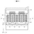
本発明の第1の観点による半導体素子は、
基板に設けられた半導体領域、及び3種類の端子電極を含み、少なくとも1つの前記端子電極は複数の導体パターンで構成された分離電極構造を持つトランジスタと、
前記分離電極構造を持つ前記端子電極の上に配置され、複数の前記導体パターンを相互に電気的に接続するバンプと、
前記トランジスタの半導体領域と前記バンプとの間に配置され、高融点金属を含む金属材料からなる応力緩和層と
を有し、
前記導体パターンと前記バンプとの間には、複数の前記導体パターンを相互に接続する電流経路が配置されていない。
The semiconductor device according to the first aspect of the present invention is
A transistor having a separation electrode structure including a semiconductor region provided on a substrate and three types of terminal electrodes, at least one of the terminal electrodes being configured of a plurality of conductor patterns;
A bump disposed on the terminal electrode having the separated electrode structure and electrically connecting a plurality of the conductor patterns to each other;
And a stress relieving layer formed between the semiconductor region of the transistor and the bump and made of a metal material containing a refractory metal.
A current path connecting the plurality of conductor patterns to each other is not disposed between the conductor pattern and the bump.
応力緩和層を配置することにより、トランジスタの半導体領域に発生する熱応力を低減させることができる。分離電極構造を持つ端子電極の複数の導体パターンがバンプによって相互に電気的に接続されているため、複数の導体パターンを相互に接続する配線層を配置する必要がない。このため、配線層の層数を少なくすることが可能になる。 By arranging the stress relieving layer, thermal stress generated in the semiconductor region of the transistor can be reduced. Since the plurality of conductor patterns of the terminal electrode having the separation electrode structure are electrically connected to each other by the bumps, it is not necessary to arrange a wiring layer which connects the plurality of conductor patterns to each other. Therefore, the number of wiring layers can be reduced.
本発明の第2の観点による半導体素子は、第1の観点による半導体素子の構成に加えて、
前記応力緩和層は、W、Mo、Ta、及びCrからなる群より選択された少なくとも1つの高融点金属を含み、その厚さが100nm以上であるという特徴を有する。
The semiconductor device according to the second aspect of the present invention is characterized in that, in addition to the configuration of the semiconductor device according to the first aspect,
The stress relieving layer includes at least one refractory metal selected from the group consisting of W, Mo, Ta, and Cr, and has a thickness of 100 nm or more.
応力緩和層をこのような構成にすることにより、熱応力を低減させる十分な効果が得られる。 Such a configuration of the stress relieving layer provides a sufficient effect of reducing thermal stress.
本発明の第3の観点による半導体素子は、第1の観点による半導体素子の構成に加えて、
前記応力緩和層は、高融点金属としてTiを含み、その厚さが300nm以上であるという特徴を有する。
The semiconductor device according to the third aspect of the present invention is, in addition to the configuration of the semiconductor device according to the first aspect,
The stress relaxation layer contains Ti as a high melting point metal and has a feature that the thickness is 300 nm or more.
応力緩和層をこのような構成にすることにより、熱応力を低減させる十分な効果が得られる。 Such a configuration of the stress relieving layer provides a sufficient effect of reducing thermal stress.
本発明の第4の観点による半導体素子は、第1から第3のまでの観点による半導体素子の構成に加えて、
前記応力緩和層は、前記バンプの下地層として形成され、前記バンプの平面形状と同一の平面形状を有するという特徴を有する。
The semiconductor device according to the fourth aspect of the present invention is characterized in that, in addition to the configuration of the semiconductor device according to the first to third aspects,
The stress relieving layer is formed as a base layer of the bump and has a feature that it has the same planar shape as the planar shape of the bump.
バンプの下地層となる応力緩和層が、バンプと半導体領域との間に配置されることにより、バンプの熱膨張率と半導体領域の熱膨張率との差に起因して半導体領域に発生する熱応力を低減させる。 The stress relieving layer serving as the base layer of the bump is disposed between the bump and the semiconductor region, whereby the heat generated in the semiconductor region due to the difference between the coefficient of thermal expansion of the bump and the coefficient of thermal expansion of the semiconductor region Reduce stress.
本発明の第5の観点による半導体素子は、第1から第3のまでの観点による半導体素子の構成に加えて、
前記応力緩和層は、前記分離電極構造を持つ前記端子電極の一部を構成するという特徴を有する。
The semiconductor device according to the fifth aspect of the present invention is characterized in that, in addition to the configuration of the semiconductor device according to the first to third aspects,
The stress relieving layer has a feature of constituting a part of the terminal electrode having the separated electrode structure.
端子電極が応力緩和層として機能することにより、半導体領域に発生する熱応力を低減させることができる。 By the terminal electrode functioning as a stress relieving layer, thermal stress generated in the semiconductor region can be reduced.
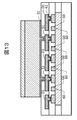
本発明の第6の観点による半導体素子は、第1から第5のまでの観点による半導体素子の構成に加えて、
さらに、前記端子電極と前記バンプとの間に配置された1つの配線層を有し、
前記バンプ及び前記導体パターンは、前記配線層に含まれる配線に、他の配線層を介することなく接続されているという特徴を有する。
The semiconductor device according to the sixth aspect of the present invention is the semiconductor device according to any one of the first to fifth aspects,
And a wiring layer disposed between the terminal electrode and the bump.
The bump and the conductor pattern are characterized in that they are connected to the wiring included in the wiring layer without interposing another wiring layer.
1層の配線層を介してバンプと複数の導体パターンとが接続され、複数の導体パターンがバンプによって相互に接続されるため、2層以上の配線層を配置する必要がない。これにより、製造コストの低減を図ることができる。 Since the bumps and the plurality of conductor patterns are connected via one wiring layer, and the plurality of conductor patterns are mutually connected by the bumps, it is not necessary to arrange two or more wiring layers. Thereby, the manufacturing cost can be reduced.
本発明の第7の観点による半導体素子は、第1から第6のまでの観点による半導体素子の構成に加えて、
前記トランジスタは、コレクタ層、ベース層、エミッタ層を含むバイポーラトランジスタであり、
3つの前記端子電極は、それぞれ前記コレクタ層、前記ベース層、及び前記エミッタ層に接続されたコレクタ電極、ベース電極、及びエミッタ電極を含むという特徴を有する。
The semiconductor device according to the seventh aspect of the present invention is the semiconductor device according to any of the first to sixth aspects,
The transistor is a bipolar transistor including a collector layer, a base layer, and an emitter layer,
Each of the three terminal electrodes includes a collector electrode connected to the collector layer, the base layer, and the emitter layer, a base electrode, and an emitter electrode.
バイポーラトランジスタの半導体領域に発生する熱応力を低減させることにより、バイポーラトランジスタの信頼性の低下、電気的特性のばらつき等を抑制することができる。 By reducing the thermal stress generated in the semiconductor region of the bipolar transistor, it is possible to suppress the reduction in the reliability of the bipolar transistor, the variation in the electrical characteristics, and the like.
本発明の第8の観点による半導体素子は、第7の観点による半導体素子の構成に加えて、
平面視において、前記バンプの内側に前記エミッタ層が配置されているという特徴を有する。
The semiconductor device according to the eighth aspect of the present invention is characterized in that, in addition to the configuration of the semiconductor device according to the seventh aspect,
In a plan view, it has a feature that the emitter layer is disposed inside the bump.
エミッタ層で発生する熱を、バンプを通して効率的に外部に放熱することができる。バンプと半導体領域との間に応力緩和層が配置されているため、平面視においてバンプの内側にエミッタ層が配置されている場合であっても、エミッタ層に発生する熱応力が低減されるため、信頼性の低下、特性のばらつき等を抑制することができる。 The heat generated in the emitter layer can be efficiently dissipated to the outside through the bumps. Since the stress relaxation layer is disposed between the bump and the semiconductor region, the thermal stress generated in the emitter layer is reduced even when the emitter layer is disposed inside the bump in plan view. It is possible to suppress the decrease in reliability, the variation in characteristics, and the like.
本発明の第9の観点による半導体素子は、第1から第6までの観点による半導体素子の構成に加えて、
前記トランジスタは、前記基板の表層部に画定された活性領域を含む電界効果トランジスタであり、
3つの前記端子電極は、それぞれ前記活性領域の上に配置されたソース電極、ドレイン電極、及びゲート電極を含むという特徴を有する。
The semiconductor device according to the ninth aspect of the present invention is the semiconductor device according to any one of the first to sixth aspects,
The transistor is a field effect transistor including an active region defined in a surface portion of the substrate,
Each of the three terminal electrodes has a feature of including a source electrode, a drain electrode, and a gate electrode disposed on the active region.
電界効果トランジスタの半導体領域に発生する熱応力を低減させることにより、電界効果トランジスタの信頼性の低下、電気的特性のばらつき等を抑制することができる。 By reducing the thermal stress generated in the semiconductor region of the field effect transistor, it is possible to suppress the decrease in the reliability of the field effect transistor, the variation in the electrical characteristics, and the like.
本発明の第10の観点による半導体素子は、第9の観点による半導体素子の構成に加えて、
平面視において、前記ゲート電極と前記活性領域とが重なる領域が前記バンプの内側に配置されているという特徴を有する。
The semiconductor device according to the tenth aspect of the present invention is characterized in that, in addition to the configuration of the semiconductor device according to the ninth aspect,
In plan view, a region in which the gate electrode and the active region overlap is disposed inside the bump.
ゲート電極と活性領域とが重なる動作領域で発生する熱を、バンプを通して効率的に外部に放熱することができる。バンプと半導体領域との間に応力緩和層が配置されているため、平面視においてバンプの内側に動作領域が配置されている場合であっても、動作領域に発生する熱応力が低減されるため、信頼性の低下、特性のばらつき等を抑制することができる。 Heat generated in an operating region where the gate electrode and the active region overlap can be dissipated efficiently to the outside through the bumps. Since the stress relieving layer is disposed between the bump and the semiconductor region, even when the operation region is disposed inside the bump in plan view, the thermal stress generated in the operation region is reduced. It is possible to suppress the decrease in reliability, the variation in characteristics, and the like.
応力緩和層を配置することにより、トランジスタの半導体領域に発生する熱応力を低減させることができる。分離電極構造を持つ端子電極の複数の導体パターンがバンプによって相互に電気的に接続されているため、複数の導体パターンを相互に接続する配線層を配置する必要がない。このため、配線層の層数を少なくすることが可能になる。 By arranging the stress relieving layer, thermal stress generated in the semiconductor region of the transistor can be reduced. Since the plurality of conductor patterns of the terminal electrode having the separation electrode structure are electrically connected to each other by the bumps, it is not necessary to arrange a wiring layer which connects the plurality of conductor patterns to each other. Therefore, the number of wiring layers can be reduced.
[第1実施例]
図1、図2、及び図3を参照して、第1実施例による半導体素子について説明する。
図1は、第1実施例による半導体素子の平面図である。半導体素子の基板の上面をxy面とし、上面の法線方向をx軸の正方向とするxyz直交座標系を定義する。第1実施例による半導体素子は、トランジスタ及びトランジスタに接続された配線、及びバンプを含む。このトランジスタは、相互に並列に接続された2つの単位トランジスタ21を含む。
[First embodiment]
The semiconductor device according to the first embodiment will be described with reference to FIGS. 1, 2 and 3. FIG.
FIG. 1 is a plan view of a semiconductor device according to the first embodiment. An xyz Cartesian coordinate system is defined in which the upper surface of the substrate of the semiconductor element is an xy plane and the normal direction of the upper surface is a positive direction of the x axis. The semiconductor device according to the first embodiment includes a transistor and a wire connected to the transistor, and a bump. This transistor includes two
2つの単位トランジスタ21は、x軸方向に並んで配置されている。単位トランジスタ21の各々は、エミッタ層、ベース層、及びコレクタ層、及びこれらにそれぞれ接続されたエミッタ電極E0、ベース電極B0、及びコレクタ電極C0を含む。図1において、エミッタ電極E0、ベース電極B0、及びコレクタ電極C0にハッチングを付している。
The two
エミッタ電極E0の各々は、y軸方向に長い長方形の平面形状を有する。ベース電極B0が、x軸方向に関して正及び負の側、及びy軸に関して正の側の三方向からエミッタ電極E0の各々を取り囲むように配置されている。x軸方向に関してベース電極B0の両側にそれぞれコレクタ電極C0が配置されている。2つの単位トランジスタ21のベース電極B0の間に配置されたコレクタ電極C0は、2つの単位トランジスタ21で共用される。
Each of emitter electrodes E0 has a rectangular planar shape elongated in the y-axis direction. The base electrode B0 is arranged to surround each of the emitter electrodes E0 from positive and negative sides with respect to the x-axis direction and three directions with respect to the y-axis and from the positive side. Collector electrodes C0 are disposed on both sides of the base electrode B0 in the x-axis direction. The collector electrode C0 disposed between the base electrodes B0 of the two
実施例による半導体素子は、1層目の配線層に配置されたエミッタ配線E1、コレクタ配線C1、及びベース配線B1を含む。1層目のエミッタ配線E1は、2つのエミッタ電極E0にそれぞれ重なるように配置された2つの孤立した導体パターンで構成され、導体パターンの各々は、その下のエミッタ電極E0に電気的に接続されている。 The semiconductor device according to the example includes an emitter wire E1, a collector wire C1, and a base wire B1 disposed in the first wiring layer. Emitter wiring E1 of the first layer is composed of two isolated conductor patterns arranged to overlap two emitter electrodes E0 respectively, and each of the conductor patterns is electrically connected to emitter electrode E0 below it ing.
1層目のコレクタ配線C1は櫛歯型の平面形状を有する。1層目のコレクタ配線C1の櫛歯部分が、それぞれコレクタ電極C0と重なるように配置されている。コレクタ電極C0を構成する複数の導体パターンは、1層目のコレクタ配線C1によって相互に接続されている。 The first-layer collector wiring C1 has a comb-like planar shape. The comb-tooth portions of the first-layer collector wiring C1 are arranged to overlap the collector electrode C0, respectively. The plurality of conductor patterns constituting the collector electrode C0 are mutually connected by the first-layer collector wiring C1.
1層目のベース配線B1は、2つの単位トランジスタ21の各々のベース電極B0を相互に接続する。
The base wiring B1 of the first layer connects the base electrodes B0 of the two
バンプ30が、1層目のエミッタ配線E1の2つの導体パターンと重なるように配置されている。バンプ30は、1層目のエミッタ配線E1の2つの導体パターンに電気的に接続されている。2つの単位トランジスタ21のエミッタ電極E0を構成する2つの導体パターンは、バンプ30により相互に電気的に接続されている。
The
図2は、図1の一点鎖線2−2における断面図である。半絶縁性のGaAsからなる基板20の上にサブコレクタ層23が配置されている。サブコレクタ層23は、高濃度のn型GaAsで形成され、その厚さは例えば0.5μmである。サブコレクタ層23の一部は、イオン注入により絶縁化されたアイソレーション領域23aとされている。サブコレクタ層23は、2つの単位トランジスタ21で共用される。
FIG. 2 is a cross-sectional view taken along dashed-dotted line 2-2 in FIG. A
サブコレクタ層23の上に、単位トランジスタ21ごとにコレクタ層24、ベース層25、及びエミッタ層26が順番に積層されている。コレクタ層24は、n型GaAsで形成され、その厚さは例えば1μmである。ベース層25はp型GaAsで形成され、その厚さは例えば100nmである。ベース層25とコレクタ層24とは、同一の平面形状を有し、コレクタメサを構成する。
A
エミッタ層26は、ベース層25の一部の領域の上に配置されている。エミッタ層26は、例えば、ベース層25側から順番に配置された厚さ30nm〜40nmのn型InGaP層、厚さ100nmの高濃度のn型GaAs層、及び厚さ100nmの高濃度のn型InGaAs層を含む。高濃度のn型InGaAs層は、その上に配置されるエミッタ電極E0とオーミックコンタクトを取るためのものである。
サブコレクタ層23の上に、コレクタ電極C0が配置されており、サブコレクタ層23にオーミックに接続されている。コレクタ電極C0は、3個の導体パターンで構成されており、3個の導体パターンは、x軸方向に関してコレクタメサの間、及び2つのコレクタメサの外側に配置されている。コレクタ電極C0は、例えば厚さ60nmのAuGe膜、厚さ10nmのNi膜、及び厚さ200nmのAu膜を積層することにより形成される。
A collector electrode C0 is disposed on the
ベース電極B0がベース層25の上に配置されており、ベース層25にオーミックに接続されている。図2に示した断面において、ベース電極B0はエミッタ層26の両側に配置されている。ベース電極B0は、例えば厚さ50nmのTi膜、厚さ50nmのPt膜、厚さ200nmのAu膜を積層することにより形成される。
The base electrode B0 is disposed on the
エミッタ層26の上にエミッタ電極E0が配置されている。エミッタ電極E0として、例えば厚さ50nmのTi膜が用いられる。
単位トランジスタ21を覆うように、絶縁膜27が配置されている。絶縁膜27として、例えばSiN膜とポリイミド等の樹脂膜との積層膜が用いられる。絶縁膜27の上面は平坦化されている。なお、絶縁膜27をSiN膜の単層で構成してもよい。
An insulating
絶縁膜27の上に、1層目のエミッタ配線E1及びコレクタ配線C1が配置されている。エミッタ配線E1は、絶縁膜27に設けられた開口を経由してエミッタ電極E0に電気的に接続されている。1層目のコレクタ配線C1は、絶縁膜27に設けられた開口を経由してコレクタ電極C0に電気的に接続されている。図2に示した断面には表れていないが、絶縁膜27の上に、1層目のベース配線B1(図1)も配置されている。ベース配線B1は、絶縁膜27に設けられた開口を経由してベース電極B0に電気的に接続されている。
On the insulating
1層目のエミッタ配線E1、コレクタ配線C1、及びベース配線B1は、例えば厚さ50nmのTi膜と、その上に配置された厚さ1μmのAu膜との2層構造を有する。 The first layer emitter wiring E1, the collector wiring C1, and the base wiring B1 have a two-layer structure of, for example, a 50 nm-thick Ti film and an 1 μm-thick Au film disposed thereon.
1層目のエミッタ配線E1、コレクタ配線C1、及びベース配線B1を覆うように、絶縁膜27の上に、上層の絶縁膜28が配置されている。絶縁膜28として、例えばSiN膜、またはSiN膜と樹脂膜との積層膜が用いられる。
An upper insulating
絶縁膜28の上に、バンプ30が配置されている。バンプ30は、絶縁膜28に1層目のエミッタ配線E1ごとに設けられた開口を経由してエミッタ配線E1に電気的に接続されている。バンプ30は、メタルポスト32、及びその上のハンダ層33を含む。バンプ30の下に、下地層としてアンダーバンプメタル層31が配置されている。
アンダーバンプメタル層31は、例えばTiで形成される。メタルポスト32として、例えば厚さ50μmのCu膜が用いられる。ハンダ層33として、例えば厚さ30μmのSn膜が用いられる。メタルポスト32とハンダ層33との間に、Ni等からなる相互拡散防止用のバリアメタル層を配置してもよい。
The under
次に、第1実施例による半導体素子の構造を採用することにより得られる優れた効果について、図3に示した比較例による半導体素子と比較しながら説明する。 Next, excellent effects obtained by adopting the structure of the semiconductor device according to the first embodiment will be described in comparison with the semiconductor device according to the comparative example shown in FIG.
図3は、比較例による半導体素子の概略平面図である。複数の単位トランジスタを並列に接続するために、コレクタまとめ配線CC、エミッタまとめ配線EC、及びベースまとめ配線BCが配置されている。コレクタまとめ配線CCは複数のコレクタ電極C0を相互に接続する。エミッタまとめ配線ECは複数のエミッタ電極E0を相互に接続する。ベースまとめ配線BCは複数のベース電極B0を相互に接続する。3種類の電極を、それぞれ対応するまとめ配線に接続するためには、通常、少なくとも2つの配線を交差させなければならない。例えば、図3に示した比較例では、エミッタ電極E0をエミッタまとめ配線ECに接続するための配線が、コレクタまとめ配線CCと交差している。このため、複数の単位トランジスタ21を並列に接続するために、少なくとも2層の配線層が必要である。
FIG. 3 is a schematic plan view of a semiconductor device according to a comparative example. In order to connect a plurality of unit transistors in parallel, collector collective wiring CC, emitter collective wiring EC, and base collective wiring BC are arranged. Collector collective wiring CC mutually connects a plurality of collector electrodes C0. Emitter collective wiring EC mutually connects a plurality of emitter electrodes E0. The base collecting wiring BC mutually connects a plurality of base electrodes B0. In order to connect the three types of electrodes to the corresponding collective wires, it is usually necessary to cross at least two wires. For example, in the comparative example shown in FIG. 3, the wiring for connecting the emitter electrode E0 to the emitter collective wiring EC intersects with the collector collective wiring CC. Therefore, at least two wiring layers are required to connect the plurality of
第1実施例では、図1に示したように、1層目のコレクタ配線C1及びベース配線B1が、それぞれコレクタまとめ配線及びベースまとめ配線としての役割を担う。1層目のエミッタ配線E1は、エミッタ電極E0の2つの導体パターンごとに配置されており、エミッタまとめ配線としての役割を持たない。第1実施例では、バンプ30がエミッタ電極E0の2つの導体パターンを相互に接続しており、エミッタまとめ配線としての役割を担う。このように、バンプ30が、本来の外部接続用の端子としての機能の他に、エミッタ電極E0の2つの導体パターンを相互に接続するまとめ配線としての機能を持つ。このため、図3に示したコレクタまとめ配線CCと交差する配線を設ける必要がない。
In the first embodiment, as shown in FIG. 1, the collector wiring C1 and the base wiring B1 of the first layer play roles as a collector collective wiring and a base collective wiring, respectively. The first layer emitter wiring E1 is disposed for each of two conductor patterns of the emitter electrode E0, and has no role as emitter collective wiring. In the first embodiment, the
上述のように、第1実施例では、必ずしも2層の配線層を設ける必要がないため、比較例(図3)に比べて配線層の層数を減らすことが可能になる。配線層の層数を減らすことにより、製造コストの低減を図ることができる。 As described above, in the first embodiment, since it is not necessary to provide two wiring layers, the number of wiring layers can be reduced as compared with the comparative example (FIG. 3). By reducing the number of wiring layers, the manufacturing cost can be reduced.
次に、アンダーバンプメタル層31(図2)を配置することにより得られる優れた効果について説明する。GaAs、InGaAs等の半導体からなるエミッタ層26、ベース層25、及びコレクタ層24の熱膨張率と、CuやSn等からなるメタルポスト32及びハンダ層33の熱膨張率との差に起因して、エミッタ層26等の半導体層に熱応力が発生する。例えば、GaAsの熱膨張率が約6ppm/℃、InGaPの熱膨張率が5ppm/℃以上6ppm/℃以下の範囲内であるのに対し、Cuの熱膨張率は17ppm/℃、Snの熱膨張率は22ppm/℃である。また、半導体素子を実装するプリント回路板の熱膨張率も、一般的に15ppm/℃以上20ppm/℃以下の範囲内である。
Next, excellent effects obtained by arranging the under bump metal layer 31 (FIG. 2) will be described. Due to the difference between the thermal expansion coefficient of
アンダーバンプメタル層31に用いられているTiの熱膨張率は8.6ppm/℃であり、半導体層の熱膨張率に近い。このため、アンダーバンプメタル層31が、半導体層に発生する熱応力を緩和する応力緩和層として機能する。
The thermal expansion coefficient of Ti used for the under
半導体層に、熱応力による歪みが発生すると、高温での通電動作時にバイポーラトランジスタの電流増幅率が低下してしまう。第1実施例では、半導体層に発生する熱応力が低減されるため、電流増幅率の低下を抑制することができる。 When strain due to thermal stress occurs in the semiconductor layer, the current amplification factor of the bipolar transistor is lowered at the time of energization operation at high temperature. In the first embodiment, since the thermal stress generated in the semiconductor layer is reduced, the reduction of the current amplification factor can be suppressed.
さらに、第1実施例では、発熱源となるエミッタ層26等がバンプ30の真下に配置されている。発熱源からバンプ30までの熱伝達経路が短くなるため、バンプ30を介した良好な放熱特性を確保することができる。この結果、バイポーラトランジスタの温度上昇による高周波特性の低下を抑制することができる。
Furthermore, in the first embodiment, the
次に、第1実施例の第1変形例について説明する。第1実施例ではアンダーバンプメタル層31(図2)にTiを用いたが、その他の高融点金属、高融点金属を含む化合物、または高融点金属を含む合金を用いてもよい。高融点金属として、Tiの他にTa、Mo、Cr、Wが挙げられる。高融点金属を含む化合物として、TaN、TiN等の高融点金属の窒化物、MoSi、WSi等の高融点金属のシリサイドが挙げられる。高融点金属を含む合金として、TiW等が挙げられる。 Next, a first modification of the first embodiment will be described. Although Ti is used for the under bump metal layer 31 (FIG. 2) in the first embodiment, other high melting point metals, compounds containing high melting point metals, or alloys containing high melting point metals may be used. In addition to Ti, Ta, Mo, Cr and W can be mentioned as the refractory metal. Examples of the compound containing a high melting point metal include nitrides of high melting point metals such as TaN and TiN, and silicides of high melting point metals such as MoSi and WSi. TiW etc. are mentioned as an alloy containing a high melting point metal.
アンダーバンプメタル層31として、SiN等の下地の絶縁膜28(図1)に対して接着性のよいTi膜と、その上に配置されたW等の応力緩和作用の高い膜とを含む多層構造を採用してもよい。このように、アンダーバンプメタル層31を、複数の金属膜からなる積層構造としてもよい。
A multi-layer structure including a Ti film having good adhesion to the underlying insulating film 28 (FIG. 1) such as SiN and a film having a high stress relaxation function such as W disposed thereon as the under
次に、図4A及び図4Bを参照して、さらに第1実施例の第2変形例及び第3変形例について説明する。
図4Aは、第1実施例の第2変形例による半導体素子の断面図である。第1実施例では、エミッタ電極E0とバンプ30とが1層目のエミッタ配線E1(図2)を介して接続されていた。第2変形例では、1層目の配線層が省略され、エミッタ電極E0とバンプ30とが配線層を介することなく電気的に接続されている。さらに、ベース用のバンプ及びコレクタ用のバンプも、それぞれベース電極B0及びコレクタ電極C0に、配線層を介することなく電気的に接続されている。
Next, with reference to FIGS. 4A and 4B, the second and third modifications of the first embodiment will be further described.
FIG. 4A is a cross-sectional view of a semiconductor device according to a second modification of the first embodiment. In the first embodiment, the emitter electrode E0 and the
第1変形例では、エミッタ電極E0、ベース電極B0、及びコレクタ電極C0と、バンプ30との間に配線層を配置する必要がないため、製造コストをより低減させることができる。
In the first modification, since it is not necessary to arrange a wiring layer between the emitter electrode E0, the base electrode B0, the collector electrode C0, and the
図4Bは、第1実施例の第3変形例による半導体素子の断面図である。第1実施例では、1層目のエミッタ配線E1がエミッタ電極E0(図2)を介してエミッタ層26に接続されていた。第3変形例では、エミッタ電極E0が省略され、1層目のエミッタ配線E1がエミッタ層26に直接接触している。すなわち、1層目のエミッタ配線E1が、第1実施例のエミッタ電極E0(図2)を兼ねている。
FIG. 4B is a cross-sectional view of a semiconductor device according to a third modification of the first embodiment. In the first embodiment, the emitter wiring E1 of the first layer is connected to the
また、コレクタ電極C0を省略し、1層目のコレクタ配線C1をサブコレクタ層23に直接オーミック接触させてもよい。さらに、ベース電極B0を省略し、1層目のベース配線B1(図1)をベース層25に直接オーミック接触させてもよい。
Also, the collector electrode C0 may be omitted, and the first-layer collector wiring C1 may be in ohmic contact with the
次に、第1実施例の第4変形例について説明する。
第1実施例による半導体素子に含まれるHBTは、3種類の端子電極、すなわちエミッタ電極E0、ベース電極B0、及びコレクタ電極C0を含む。第1実施例による半導体素子では、複数のコレクタ電極C0が1層目のコレクタ配線C1により相互に電気的に接続され、複数のベース電極B0が1層目のベース配線B1により相互に電気的に接続されている。これに対し、エミッタ電極E0を構成する複数の導体パターンは、バンプ30により相互に電気的に接続されており、エミッタ電極E0とバンプ30との間の配線層には、エミッタ電極E0の複数の導体パターンを相互に接続する電流経路は配置されていない。
Next, a fourth modification of the first embodiment will be described.
The HBT included in the semiconductor device according to the first embodiment includes three types of terminal electrodes: an emitter electrode E0, a base electrode B0, and a collector electrode C0. In the semiconductor device according to the first embodiment, the plurality of collector electrodes C0 are electrically connected to each other by the first-layer collector wiring C1, and the plurality of base electrodes B0 are electrically connected to each other by the first-layer base wiring B1. It is connected. On the other hand, the plurality of conductor patterns constituting the emitter electrode E0 are electrically connected to each other by the
第4変形例では、コレクタ電極C0を構成する複数の導体パターンがバンプによって相互に接続されており、コレクタ電極C0とバンプとの間には、コレクタ電極C0を構成する複数の導体パターンを相互に接続する電流経路が配置されていない。エミッタ電極E0を構成する複数の導体パターンは、1層目のエミッタ配線E1により相互に電気的に接続されている。 In the fourth modification, a plurality of conductor patterns constituting collector electrode C0 are mutually connected by bumps, and a plurality of conductor patterns constituting collector electrode C0 are mutually connected between collector electrode C0 and a bump. There is no current path to connect. The plurality of conductor patterns constituting the emitter electrode E0 are electrically connected to each other by the first layer emitter wiring E1.
ベース電極B0を構成する複数の導体パターンをバンプによって相互に接続し、ベース電極B0とバンプとの間に、ベース電極B0を構成する複数の導体パターンを相互に接続する電流経路を配置しない構成としてもよい。 As a configuration in which a plurality of conductor patterns forming base electrode B0 are connected to one another by bumps, and a current path connecting a plurality of conductor patterns forming base electrode B0 is not disposed between base electrode B0 and bumps. It is also good.
また、第1実施例では、エミッタ電極E0の平面形状を長方形にしたが、その他の形状、例えば八角形等の多角形にしてもよい。エミッタ電極E0の形状に合わせて、その下のエミッタ層26の平面形状も、八角形等の多角形にしてもよい。
In the first embodiment, the planar shape of the emitter electrode E0 is a rectangle, but it may be another shape, for example, a polygon such as an octagon. According to the shape of the emitter electrode E0, the planar shape of the
[第2実施例]
次に、図5、図6、及び図7を参照して、第2実施例による半導体素子について説明する。以下、第1実施例による半導体素子と共通の構成については説明を省略する。
Second Embodiment
Next, a semiconductor device according to a second embodiment will be described with reference to FIGS. 5, 6, and 7. FIG. Hereinafter, the description of the same configuration as the semiconductor device according to the first embodiment will be omitted.
図5は、第2実施例による半導体素子の平面図である。第1実施例では2個の単位トランジスタ21(図1)を並列接続したが、第2実施例では、3個以上の複数、例えば10個の単位トランジスタ21を並列接続することによりHBTが構成される。10個の単位トランジスタ21は、x軸方向に並んで配置されている。単位トランジスタ21の各々は、エミッタ電極E0、ベース電極B0、及びコレクタ電極C0を含む。図5において、エミッタ電極E0、ベース電極B0、及びコレクタ電極C0にハッチングを付している。
FIG. 5 is a plan view of the semiconductor device according to the second embodiment. In the first embodiment, two unit transistors 21 (FIG. 1) are connected in parallel, but in the second embodiment, an HBT is configured by connecting three or more, for example, ten
1層目のエミッタ配線E1が、10個のエミッタ電極E0に対応して10個の導電パターンにより構成される。1層目のコレクタ配線C1が、コレクタ電極C0を構成する複数の導体パターンを相互に接続する。複数の1層目のベース配線B1が、それぞれベース電極B0を構成する複数の導体パターンに接続されている。 Emitter wiring E1 of the first layer is formed of ten conductive patterns corresponding to ten emitter electrodes E0. The first-layer collector wiring C1 mutually connects a plurality of conductor patterns constituting the collector electrode C0. The plurality of first layer base wirings B1 are connected to the plurality of conductor patterns constituting the base electrode B0, respectively.
第1実施例では、x軸方向に関してベース電極B0がエミッタ電極E0の両側に配置されていたが、第2実施例では、エミッタ電極E0の片側(x軸の負の側)にのみベース電極B0が配置されている。 In the first embodiment, the base electrode B0 is disposed on both sides of the emitter electrode E0 in the x-axis direction, but in the second embodiment, the base electrode B0 is disposed on only one side (negative side of the x axis) of the emitter electrode E0. Is arranged.
バンプ30は、x軸方向に長い長方形の両端に半円を接続したレーストラック形状を有する。平面視において1層目のコレクタ配線C1の内側に、複数のコレクタ用のバンプ35が配置されており、1層目のコレクタ配線C1は、コレクタ用のバンプ35に電気的に接続されている。
The
図6は、図5の一点鎖線6−6における断面図である。基板20、コレクタ層24、及びベース層25の構成は、第1実施例によるこれらの構成と同一である。エミッタ層26は、第1実施例による半導体素子のエミッタ層26(図2)と同様に、n型InGaP層、高濃度のn型GaAs層、及び高濃度のn型InGaAs層を含む。
6 is a cross-sectional view taken along an alternate long and short dash line 6-6 in FIG. The structures of the
第2実施例では、最も下のn型InGaP層がベース層25の上面の全域の上に配置されている。n型InGaP層の一部の領域の上に、n型GaAs層とn型InGaAs層とからなるエミッタメサ層26Bが配置されている。n型InGaP層のうちエミッタメサ層26Bが配置されていない領域は空乏化している。空乏化している領域をレッジ層26Cという。n型InGaP層のうちエミッタメサ層26Bと重なる領域を、真性エミッタ層26Aという。真性エミッタ層26Aとエミッタメサ層26Bとが、第1実施例による半導体素子のエミッタ層26(図2)に相当する。
In the second embodiment, the lowermost n-type InGaP layer is disposed on the entire top surface of the
レッジ層26Cに設けられた開口内にベース電極B0が配置されている。エミッタ電極E0及びコレクタ電極C0の構成は、第1実施例による半導体素子のエミッタ電極E0及びコレクタ電極C0(図2)の構成と同一である。
The base electrode B0 is disposed in the opening provided in the
単位トランジスタ21を覆うようにSiNからなる絶縁膜27が配置されている。第1実施例では、絶縁膜27(図2)の上面が平坦化されていたが、第2実施例では、絶縁膜27の上面は平坦化されていない。
An insulating
絶縁膜27の上に配置された1層目のエミッタ配線E1及びコレクタ配線C1が、それぞれ絶縁膜27に設けられた開口を経由してエミッタ電極E0及びコレクタ電極C0に電気的に接続されている。1層目のエミッタ配線E1及びコレクタ配線C1として、例えば厚さ1μmのAu膜が用いられる。
The first layer emitter wiring E1 and collector wiring C1 disposed on the insulating
1層目のエミッタ配線E1及びコレクタ配線C1を絶縁膜28が覆う。絶縁膜28は、樹脂膜28A、SiN膜28B、及び樹脂膜28Cがこの順番に積層された3層構造を有する。絶縁膜28の上面は平坦化されている。絶縁膜28の上のアンダーバンプメタル層31及びバンプ30の構造は、第1実施例による半導体素子(図2)のこれらの構造と同一である。
The insulating
複数の単位トランジスタ21の真性エミッタ層26Aは、エミッタメサ層26B、エミッタ電極E0、及び1層目のエミッタ配線E1を介して、バンプ30により相互に接続されている。複数の単位トランジスタ21のコレクタ層24は、サブコレクタ層23、コレクタ電極C0を介して、1層目のコレクタ配線C1により相互に接続されている。
The intrinsic emitter layers 26A of the plurality of
複数の単位トランジスタ21のベース層25は、ベース電極B0を介して1層目のベース配線B1(図1)に接続されている。図1では、複数のベース電極B0が1層目のベース配線B1により相互い接続されている例を示したが、単位トランジスタ21の各々のベース層25には、バラスト抵抗、高周波入力用のキャパシタ等を接続することが好ましい。ベース層25は、バラスト抵抗を介してバイアス回路に接続され、キャパシタを介して高周波入力用のバンプに接続される。なお、ベース層25は、キャパシタ、及び同一基板上のマッチング回路を介して高周波入力用のバンプに接続してもよい。
The base layers 25 of the plurality of
第2実施例による半導体素子は、エミッタ用のバンプ30、コレクタ用のバンプ35(図5)、高周波入力用のバンプ等を実装基板のランド等にハンダ付けすることにより、実装基板に実装される。実装基板として、例えばアルミナ等のセラミック基板、樹脂基板等が用いられる。
The semiconductor device according to the second embodiment is mounted on the mounting substrate by soldering the
次に、図7を参照して、エミッタ層26に発生する熱応力をシミュレーションにより求めた結果について説明する。シミュレーションにおいて、真性エミッタ層26A(図6)のy軸方向の寸法(長さ)を30μmとし、x軸方向の寸法(幅)を4μmとした。10本の真性エミッタ層26A(図5)のうち1本を取り出して熱応力を計算した。バンプ30(図5)は、長さ240μm、幅75μmの長方形の短辺に直径75μmの半円を接続したレーストラック形状とした。樹脂膜28A、28Cの各々の厚さを1.5μmとし、SiN膜28Bの厚さを0.5μmとした。半導体素子の温度を、ハンダの接合温度付近の230℃から150℃まで下降させたときに真性エミッタ層26Aに発生する熱応力を計算した。
Next, the thermal stress generated in the
図7は、応力緩和層として機能するアンダーバンプメタル層31が配置されていない場合を基準としたときの、真性エミッタ層26Aに発生する熱応力の最大値の変化率を示すグラフである。横軸は応力緩和層として機能するアンダーバンプメタル層31の厚さを単位「μm」で表し、縦軸は応力変化率を単位「%」で表す。負の応力変化率は、熱応力が低減されていることを意味する。応力変化率の絶対値が大きいことは、熱応力が小さいことを意味する。アンダーバンプメタル層31にTi、Ta、Mo、Cr、Wの5種類の高融点金属を用いた場合についてシミュレーションを行った。Ti、Ta、Mo、Cr、Wの熱膨張率は、それぞれ8.6ppm/℃、6.3ppm/℃、5.1ppm/℃、4.9ppm/℃、4.5ppm/℃である。
FIG. 7 is a graph showing the change rate of the maximum value of the thermal stress generated in the
アンダーバンプメタル層31が厚くなるに従って熱応力が低下することがわかる。これは、アンダーバンプメタル層31の材料の熱膨張率が、半導体素子を構成する半導体材料の熱膨張率に近いためである。このシミュレーションにより、アンダーバンプメタル層31が、熱応力を緩和させる機能を有していることが確認された。
It can be seen that the thermal stress decreases as the under
[第3実施例]
次に、図8及び図9を参照して、第3実施例による半導体素子について説明する。以下、図5、図6、図7に示した第2実施例による半導体素子と共通の構成については説明を省略する。
Third Embodiment
A semiconductor device according to a third embodiment will now be described with reference to FIGS. 8 and 9. The description of the same configuration as that of the semiconductor device according to the second embodiment shown in FIGS. 5, 6 and 7 will be omitted.
図8は、第3実施例による半導体素子の断面図である。第2実施例では、バンプ30の下地層として用いられるアンダーバンプメタル層31(図6)が応力緩和層として機能した。第3実施例では、アンダーバンプメタル層31が配置されておらず、その代わりに1層目のエミッタ配線E1の下に、応力緩和層41が配置されている。1層目のエミッタ配線E1は、応力緩和層41を介してエミッタ電極E0に接続される。
FIG. 8 is a cross-sectional view of the semiconductor device according to the third embodiment. In the second embodiment, the under bump metal layer 31 (FIG. 6) used as the underlayer of the
図9は、応力緩和層41が配置されていない場合を基準としたときの、真性エミッタ層26A(図8)に発生する熱応力の最大値の変化率を示すグラフである。横軸は応力緩和層41の厚さを単位「μm」で表し、縦軸は応力変化率を単位「%」で表す。応力緩和層にTi、Ta、Mo、Wの4種類の高融点金属を用いた場合についてシミュレーションを行った。
FIG. 9 is a graph showing the rate of change of the maximum value of the thermal stress generated in the
応力緩和層41が厚くなるに従って熱応力が低下しており、応力緩和層41が、熱応力を緩和させる機能を有していることが確認された。図8に示した例では、応力緩和層41を1層目のエミッタ配線E1の下に配置したが、応力緩和層41は、1層目のエミッタ配線E1の上または内部に配置してもよい。 The thermal stress decreased as the stress relieving layer 41 became thicker, and it was confirmed that the stress relieving layer 41 has a function of relieving the thermal stress. In the example shown in FIG. 8, the stress relieving layer 41 is disposed under the first layer emitter wire E1, but the stress relieving layer 41 may be disposed on or in the first layer emitter wire E1. .
[第4実施例]
次に、図10を参照して、第4実施例による半導体素子について説明する。以下、図5、図6、図7に示した第2実施例による半導体素子と共通の構成については説明を省略する。
Fourth Embodiment
A semiconductor device according to the fourth embodiment will now be described with reference to FIG. The description of the same configuration as that of the semiconductor device according to the second embodiment shown in FIGS. 5, 6 and 7 will be omitted.
第2実施例では、エミッタ電極E0として厚さ50nmのTi膜を用いたが、第4実施例では、エミッタ電極E0を構成するTi膜をより厚くするか、エミッタ電極E0にTi以外の高融点金属を用いる。また、応力緩和層として機能するアンダーバンプメタル層31(図6)は配置しない。 In the second embodiment, a Ti film of 50 nm in thickness is used as the emitter electrode E0, but in the fourth embodiment, the Ti film constituting the emitter electrode E0 is made thicker or a high melting point other than Ti is used for the emitter electrode E0. Use metal. Also, the under bump metal layer 31 (FIG. 6) which functions as a stress relieving layer is not disposed.
図10は、応力緩和層として機能するエミッタ電極E0が配置されていない場合を基準としたときの、真性エミッタ層26Aに発生する熱応力の最大値の変化率を示すグラフである。横軸はエミッタ電極E0の厚さを単位「μm」で表し、縦軸は応力変化率を単位「%」で表す。エミッタ電極E0にTi、Ta、Mo、Wの4種類の高融点金属を用いた場合についてシミュレーションを行った。
FIG. 10 is a graph showing the rate of change of the maximum value of thermal stress generated in the
エミッタ電極E0が厚くなるに従って熱応力が低下しており、エミッタ電極E0が、熱応力を緩和させる機能を有していることが確認された。 The thermal stress decreased as the emitter electrode E0 became thicker, and it was confirmed that the emitter electrode E0 has a function of relieving the thermal stress.
[応力緩和層の厚さ]
次に、第2実施例、第3実施例、及び第4実施例による半導体素子における応力変化率のシミュレーション結果から導き出される応力緩和層の好ましい厚さについて説明する。アンダーバンプメタル層31(図6)、応力緩和層41(図8)、及びエミッタ電極E0(図10)等の応力緩和層のいずれも極めて薄くしてHBTの寿命試験を行った。その結果、短時間でHBTが劣化し、このHBTを実使用に適用することが困難であることが判明した。これは、熱応力によって真性エミッタ層26A等の半導体層がダメージを受けるためである。応力緩和層を配置することによって真性エミッタ層26Aに発生する熱応力を2%低減させると、HBTの寿命が約35倍に延びた。この寿命は、実使用に耐える範囲である。
[Thickness of stress relaxation layer]
Next, the preferable thickness of the stress relaxation layer derived from the simulation results of the stress change rate in the semiconductor device according to the second embodiment, the third embodiment, and the fourth embodiment will be described. Each of the stress relieving layers such as the under bump metal layer 31 (FIG. 6), the stress relieving layer 41 (FIG. 8), and the emitter electrode E0 (FIG. 10) was made extremely thin to conduct the life test of the HBT. As a result, it turned out that HBT deteriorates in a short time, and it is difficult to apply this HBT to real use. This is because the semiconductor layer such as the
応力緩和層を配置しない場合の熱応力を基準としたときの応力変化率の絶対値が2%以上になると、HBTの寿命はさらに延びる。ただし、応力変化率の絶対値が2%以上の範囲では、寿命の延び方は緩やかである。例えば、応力変化率が−28%の場合、HBTの寿命の延びは高々41倍であった。これらの評価実験から、HBTの長寿命化を図るために、応力緩和層を配置しない場合に比べて、真性エミッタ層26Aに発生する熱応力を2%以上低減させることが好ましいと考えられる。
When the absolute value of the stress change rate is 2% or more based on the thermal stress when the stress relaxation layer is not disposed, the life of the HBT is further extended. However, in the range where the absolute value of the stress change rate is 2% or more, how to extend the life is slow. For example, when the stress change rate is -28%, the extension of the life of the HBT was at most 41 times. From these evaluation experiments, it is considered preferable to reduce the thermal stress generated in the
図7、図9、及び図10に示したシミュレーション結果から、HBTの長寿命化を図るために、高融点金属としてTa、Mo、Cr、またはWを用いた応力緩和層の厚さを100nm以上にすることにより、十分な寿命を確保することができると考えられる。また、これらの高融点金属を含む合金または化合物からなる応力緩和層を用いる場合にも、応力緩和層の厚さを100nm以上にすることにより、十分な寿命を確保することができると考えられる。 From the simulation results shown in FIG. 7, FIG. 9 and FIG. 10, the thickness of the stress relaxation layer using Ta, Mo, Cr or W as the refractory metal is 100 nm or more in order to prolong the life of the HBT. It can be considered that a sufficient life can be secured by In addition, even in the case of using a stress relaxation layer made of an alloy or compound containing such high melting point metals, it is considered that a sufficient life can be secured by setting the thickness of the stress relaxation layer to 100 nm or more.
高融点金属としてTiを用いた応力緩和層の厚さを300nm以上にすることにより、十分な寿命を確保することができると考えられる。また、Tiを含む合金または化合物からなる応力緩和層を用いる場合にも、応力緩和層の厚さを300nm以上にすることにより、十分な寿命を確保することができると考えられる。 By setting the thickness of the stress relaxation layer using Ti as a high melting point metal to 300 nm or more, it is considered that a sufficient life can be secured. Further, also in the case of using a stress relaxation layer made of an alloy or a compound containing Ti, it is considered that a sufficient life can be secured by setting the thickness of the stress relaxation layer to 300 nm or more.
応力緩和層が、Ta、Mo、Cr、及びWから選択された1つの高融点金属と、Tiとを含む場合には、応力緩和層の厚さを100nm以上にすればよい。例えば、応力緩和層にTiW合金を用いる場合には、その厚さを100nm以上にすればよく、TiAl合金を用いる場合には、その厚さを300nm以上にすればよい。 When the stress relieving layer contains one refractory metal selected from Ta, Mo, Cr, and W, and Ti, the thickness of the stress relieving layer may be 100 nm or more. For example, when using a TiW alloy for the stress relaxation layer, its thickness may be 100 nm or more, and when using a TiAl alloy, its thickness may be 300 nm or more.
応力緩和層を厚くしすぎることは、電気抵抗の観点から好ましくない。HBTの性能を決めるエミッタ抵抗の実用上の値は、エミッタ面積100μm2当たり0.1Ω程度である。応力緩和層の抵抗値は、このエミッタ抵抗の実用上の値より1桁以上小さくすることが好ましい。すなわち、0.01Ω以下にすることが好ましい。応力緩和層に用いられるTi、Ta、Mo、Cr、W等の電気抵抗率は、概ね10−7Ωmのオーダである。応力緩和層がエミッタ面積と同程度の開口でエミッタ電極に接していると仮定すると、応力緩和層の抵抗を0.01Ω以下にするために、応力緩和層の厚さを、例えば10μm以下にすることが好ましい。 Making the stress relaxation layer too thick is not preferable from the viewpoint of electrical resistance. The practical value of the emitter resistance which determines the performance of the HBT is about 0.1 Ω per 100 μm 2 of emitter area. The resistance value of the stress relieving layer is preferably one digit or more smaller than the practical value of the emitter resistance. That is, it is preferable to make it 0.01 Ω or less. The electrical resistivity of Ti, Ta, Mo, Cr, W or the like used for the stress relaxation layer is on the order of 10 -7 Ωm. Assuming that the stress relieving layer is in contact with the emitter electrode at the same opening as the emitter area, the thickness of the stress relieving layer is, for example, 10 μm or less in order to make the resistance of the stress relieving layer 0.01 Ω or less. Is preferred.
[第5実施例]
次に、図11及び図12を参照して、第5実施例による半導体素子について説明する。以下、第1実施例による半導体素子と共通の構成については説明を省略する。第1実施例による半導体素子はバイポーラトランジスタを含んでいたが、第5実施例による半導体素子は、バイポーラトランジスタの代わりに電界効果トランジスタ(FET)を含む。
Fifth Embodiment
A semiconductor device according to a fifth embodiment will now be described with reference to FIGS. 11 and 12. Hereinafter, the description of the same configuration as the semiconductor device according to the first embodiment will be omitted. The semiconductor device according to the first embodiment includes a bipolar transistor, but the semiconductor device according to the fifth embodiment includes a field effect transistor (FET) instead of the bipolar transistor.
図11は、第5実施例による半導体素子の平面図である。基板の上面をxy面とし、上面の法線方向をz軸の正方向とするxyz直交座標系を定義する。x軸方向に複数の単位トランジスタ21が並んでいる。複数の単位トランジスタ21が並列に接続されることにより、1つの電界効果トランジスタを構成している。図11では、4個の単位トランジスタ21が配置されている例を示している。単位トランジスタ21の各々は、MESFETである。
FIG. 11 is a plan view of the semiconductor device according to the fifth embodiment. An xyz Cartesian coordinate system is defined in which the upper surface of the substrate is the xy plane and the normal direction of the upper surface is the positive direction of the z axis. A plurality of
単位トランジスタ21の各々は、ゲート電極G0、ソース電極S0、及びドレイン電極D0を含む。図11において、ゲート電極G0、ソース電極S0、及びドレイン電極D0にハッチングを付している。x軸方向に長い長方形の活性領域50と、y軸方向に長い4本のゲート電極G0の各々とが交差している。複数のゲート電極G0は、活性領域50の外側で相互に連結されている。例えば、図11において、左側の2本のゲート電極G0が相互に連結されており、右側の2本のゲート電極G0が相互に連結されている。全てのゲート電極G0は、1層目のゲート配線G1に電気的に接続されている。
Each
ゲート電極G0の各々の一方の側にドレイン電極D0が配置され、他方の側にソース電極S0が配置されている。相互に隣り合う単位トランジスタ21は、1つのソース電極S0または1つのドレイン電極D0を共用している。図11では、2本のソース電極S0及び3本のドレイン電極D0が配置されている例を示している。
The drain electrode D0 is disposed on one side of each of the gate electrodes G0, and the source electrode S0 is disposed on the other side. The
櫛歯型の1層目のドレイン配線D1の櫛歯部分が、それぞれ3本のドレイン電極D0に重なって配置されており、ドレイン電極D0に電気的に接続されている。1層目のドレイン配線D1の複数の櫛歯部分は、活性領域50の外側において相互に連結されている。
The comb-tooth portions of the first-layer drain wiring D1 of the comb-tooth shape are disposed so as to overlap the three drain electrodes D0, respectively, and are electrically connected to the drain electrode D0. The plurality of comb teeth portions of the first layer drain wiring D1 are mutually connected outside the
ソース電極S0に重なるように1層目のソース配線S1が配置されている。ソース配線S1は、ソース電極S0のそれぞれに対応して配置された複数の導体パターンで構成される。1層目のソース配線S1を構成する複数の導体パターンは、バンプ30により相互に電気的に接続されている。
Source wiring S1 of the first layer is arranged to overlap source electrode S0. Source interconnection S1 is formed of a plurality of conductor patterns arranged corresponding to each of source electrodes S0. The plurality of conductor patterns constituting the first layer source wiring S1 are electrically connected to each other by the
活性領域50とゲート電極G0とが重なっている部分が、FETの動作においてドレイン電流が制御される部分である。本明細書において、活性領域50とゲート電極G0とが重なっている部分を動作領域60ということとする。複数の動作領域60は、平面視においてバンプ30の内側に配置されている。
The portion where the
図12は、図11の一点鎖線12−12における断面図である。半絶縁性のGaAsからなる基板51の上にn型GaAsからなるチャネル層52がエピタキシャル成長されている。チャネル層52の一部の領域は、イオン注入技術によって絶縁化されてアイソレーション領域52aとされている。アイソレーション領域52aにより、活性領域50が画定される。
FIG. 12 is a cross-sectional view taken along dashed-dotted line 12-12 in FIG. A
チャネル層52に接するように、2本のソース電極S0、4本のゲート電極G0、及び3本のドレイン電極D0が配置されている。これらの電極を覆うように、絶縁膜55が配置されている。絶縁膜55は、例えばSiN膜からなる単層構造、またはSiN膜とポリイミド膜からなる2層構造を有する。
Two
絶縁膜55の上に1層目のドレイン配線D1及びソース配線S1が配置されている。1層目のドレイン配線D1は、絶縁膜55に設けられた開口を経由してドレイン電極D0に電気的に接続されている。1層目のソース配線S1は、絶縁膜55に設けられた開口を経由してソース電極S0に電気的に接続されている。絶縁膜55の上には、1層目のゲート配線G1(図11)も配置されている。1層目のドレイン配線D1、ソース配線S1、及びゲート配線G1は、例えば厚さ50nmのTi膜と、その上に配置された厚さ1μmのAu膜との2層構造を有する。
The drain wiring D1 and the source wiring S1 of the first layer are disposed on the insulating
これらの1層目の配線を覆うように、絶縁膜55の上に上層の絶縁膜56が配置されている。絶縁膜56は、例えばSiN膜からなる単層構造、またはSiN膜とポリイミド膜からなる2層構造を有する。
An upper insulating
絶縁膜56の上にバンプ30が配置されている。バンプ30は、第1実施例による半導体素子のバンプ30(図2)と同様に、メタルポスト32、及びハンダ層33からなる2層構造を有する。バンプ30の下地層として、アンダーバンプメタル層31が配置されている。アンダーバンプメタル層31は、第1実施例による半導体素子の場合と同様に、応力緩和層として機能する。
次に、第5実施例による半導体素子の構成を採用することにより得られる優れた効果について説明する。 Next, excellent effects obtained by adopting the configuration of the semiconductor device according to the fifth embodiment will be described.
FETの真上にバンプが配置されていると、バンプ材料と半導体材料との熱膨張率の相違により、FETの半導体領域に熱応力が発生しやすくなる。半導体領域、特に動作領域60に熱応力が発生すると、FETの信頼度の低下、電気的特性のばらつき、特性不良等が起きやすくなる。特に、GaAs等の化合物半導体からなるチャネル層52では、ゲート電極G0の近傍に発生する熱応力によりピエゾ電荷が発生する。このピエゾ電荷によって、閾値電圧の変動等が発生し、特性のばらつきが大きくなる。
When the bumps are disposed directly above the FET, thermal stress is easily generated in the semiconductor region of the FET due to the difference in thermal expansion coefficient between the bump material and the semiconductor material. When thermal stress is generated in the semiconductor region, particularly in the
第5実施例では、アンダーバンプメタル層31が応力緩和層として機能するため、熱応力に起因する特性のばらつき、特性の不良、信頼性の低下等を抑制することができる。
In the fifth embodiment, since the under
さらに、1層目のソース配線S1を構成する複数の導体パターンをバンプ30によって相互に電気的に接続しているため、これらの導体パターンを接続するための他の配線層を配置する必要がない。このため、配線層の層数を少なくすることが可能になり、その結果、製造コストの低減を図ることができる。
Furthermore, since the plurality of conductor patterns constituting the first layer source wiring S1 are electrically connected to each other by the
次に、図13を参照して、第5実施例の変形例による半導体素子について説明する。第5実施例では、アンダーバンプメタル層31を応力緩和層として用いたが、本変形例では、第3実施例による半導体素子の応力緩和層41(図8)と同様に、1層目のソース配線S1及びドレイン配線D1の下に、応力緩和層42を配置する。応力緩和層42が動作領域60の真上に配置されるように、ソース配線S1及びドレイン配線D1をゲート電極G0の真上まで延伸させている。これにより、動作領域60に発生し得る応力を低減させることができる。応力緩和層42を配置する場合には、アンダーバンプメタル層31に応力を緩和させる機能を持たせなくてもよい。このため、第5実施例の場合と比べて、アンダーバンプメタル層31を薄くしてもよい。
Next, a semiconductor device according to a modification of the fifth embodiment will be described with reference to FIG. In the fifth embodiment, the under
その他に、第4実施例による半導体素子の応力緩和層として機能するエミッタ電極E0(図6)と同様に、ゲート電極G0を高融点金属で形成し、応力緩和層として機能させてもよい。また、ゲート電極G0の一部を高融点金属からなる層にしてもよい。 In addition, as with the emitter electrode E0 (FIG. 6) functioning as a stress relaxation layer of the semiconductor device according to the fourth embodiment, the gate electrode G0 may be formed of a high melting point metal and function as a stress relaxation layer. Further, part of the gate electrode G0 may be made of a layer made of high melting point metal.
このように、1層目の配線層またはゲート電極G0の一部に応力緩和層を配置しても、第5実施例と同様に、動作領域60に発生する熱応力を低減させることができる。
As described above, even if the stress relaxation layer is disposed in the first wiring layer or in part of the gate electrode G0, the thermal stress generated in the
上述の各実施例は例示であり、異なる実施例で示した構成の部分的な置換または組み合わせが可能であることは言うまでもない。複数の実施例の同様の構成による同様の作用効果については実施例ごとには逐次言及しない。さらに、本発明は上述の実施例に制限されるものではない。例えば、種々の変更、改良、組み合わせ等が可能なことは当業者に自明であろう。 It goes without saying that the above-described embodiments are exemplification, and partial replacement or combination of the configurations shown in the different embodiments is possible. Similar advantages and effects resulting from similar configurations of the multiple embodiments will not be sequentially described in each embodiment. Furthermore, the invention is not limited to the embodiments described above. For example, it will be apparent to those skilled in the art that various modifications, improvements, combinations, and the like can be made.
20 基板
21 単位トランジスタ
23 サブコレクタ層
23a アイソレーション領域
24 コレクタ層
25 ベース層
26 エミッタ層
26A 真性エミッタ層
26B エミッタメサ層
26C レッジ層
27、28 絶縁膜
28A 樹脂膜
28B SiN膜
28C 樹脂膜
30 エミッタ用のバンプ
31 アンダーバンプメタル層
32 メタルポスト
33 ハンダ層
35 コレクタ用のバンプ
41 応力緩和層
50 活性領域
51 基板
52 チャネル層
52a アイソレーション領域
55、56 絶縁膜
60 動作領域
B0 ベース電極
B1 1層目のベース配線
BC ベースまとめ配線
C0 コレクタ電極
C1 1層目のコレクタ配線
CC コレクタまとめ配線
D0 ドレイン電極
D1 1層目のドレイン配線
E0 エミッタ電極
E1 1層目のエミッタ配線
EC エミッタまとめ配線
G0 ゲート電極
G1 1層目のゲート配線
S0 ソース電極
S1 1層目のソース配線
図1、図2、及び図3を参照して、第1実施例による半導体素子について説明する。
図1は、第1実施例による半導体素子の平面図である。半導体素子の基板の上面をxy面とし、上面の法線方向をz軸の正方向とするxyz直交座標系を定義する。第1実施例による半導体素子は、トランジスタ及びトランジスタに接続された配線、及びバンプを含む。このトランジスタは、相互に並列に接続された2つの単位トランジスタ21を含む。
The semiconductor device according to the first embodiment will be described with reference to FIGS. 1, 2 and 3. FIG.
FIG. 1 is a plan view of a semiconductor device according to the first embodiment. An xyz Cartesian coordinate system is defined in which the upper surface of the substrate of the semiconductor element is an xy plane and the normal direction of the upper surface is a positive direction of the z axis . The semiconductor device according to the first embodiment includes a transistor and a wire connected to the transistor, and a bump. This transistor includes two
第2変形例では、エミッタ電極E0、ベース電極B0、及びコレクタ電極C0と、バンプ30との間に配線層を配置する必要がないため、製造コストをより低減させることができる。
In the second modification, since it is not necessary to arrange a wiring layer between the emitter electrode E0, the base electrode B0, the collector electrode C0, and the
Claims (10)
前記分離電極構造を持つ前記端子電極の上に配置され、複数の前記導体パターンを相互に電気的に接続するバンプと、
前記トランジスタの半導体領域と前記バンプとの間に配置され、高融点金属を含む金属材料からなる応力緩和層と
を有し、
前記導体パターンと前記バンプとの間には、複数の前記導体パターンを相互に接続する電流経路が配置されていない半導体素子。 A transistor having a separation electrode structure including a semiconductor region provided on a substrate and three types of terminal electrodes, at least one of the terminal electrodes being configured of a plurality of conductor patterns;
A bump disposed on the terminal electrode having the separated electrode structure and electrically connecting a plurality of the conductor patterns to each other;
And a stress relieving layer formed between the semiconductor region of the transistor and the bump and made of a metal material containing a refractory metal.
A semiconductor element in which a current path connecting the plurality of conductor patterns to each other is not disposed between the conductor pattern and the bump.
前記バンプ及び前記導体パターンは、前記配線層に含まれる配線に、他の配線層を介することなく接続されている請求項1乃至5のいずれか1項に記載の半導体素子。 And a wiring layer disposed between the terminal electrode and the bump.
The semiconductor element according to any one of claims 1 to 5, wherein the bump and the conductor pattern are connected to the wiring included in the wiring layer without interposing another wiring layer.
3つの前記端子電極は、それぞれ前記コレクタ層、前記ベース層、及び前記エミッタ層に接続されたコレクタ電極、ベース電極、及びエミッタ電極を含む請求項1乃至6のいずれか1項に記載の半導体素子。 The transistor is a bipolar transistor including a collector layer, a base layer, and an emitter layer,
The semiconductor device according to any one of claims 1 to 6, wherein the three terminal electrodes respectively include the collector layer, the base layer, and a collector electrode connected to the emitter layer, a base electrode, and an emitter electrode. .
3つの前記端子電極は、それぞれ前記活性領域の上に配置されたソース電極、ドレイン電極、及びゲート電極を含む請求項1乃至6のいずれか1項に記載の半導体素子。 The transistor is a field effect transistor including an active region defined in a surface portion of the substrate,
The semiconductor device according to any one of claims 1 to 6, wherein the three terminal electrodes each include a source electrode, a drain electrode, and a gate electrode disposed on the active region.
Priority Applications (3)
| Application Number | Priority Date | Filing Date | Title |
|---|---|---|---|
| JP2017234277A JP2019102724A (en) | 2017-12-06 | 2017-12-06 | Semiconductor element |
| US16/209,391 US10566303B2 (en) | 2017-12-06 | 2018-12-04 | Semiconductor element |
| CN201811476472.9A CN109994430A (en) | 2017-12-06 | 2018-12-04 | Semiconductor element |
Applications Claiming Priority (1)
| Application Number | Priority Date | Filing Date | Title |
|---|---|---|---|
| JP2017234277A JP2019102724A (en) | 2017-12-06 | 2017-12-06 | Semiconductor element |
Publications (1)
| Publication Number | Publication Date |
|---|---|
| JP2019102724A true JP2019102724A (en) | 2019-06-24 |
Family
ID=66658521
Family Applications (1)
| Application Number | Title | Priority Date | Filing Date |
|---|---|---|---|
| JP2017234277A Pending JP2019102724A (en) | 2017-12-06 | 2017-12-06 | Semiconductor element |
Country Status (3)
| Country | Link |
|---|---|
| US (1) | US10566303B2 (en) |
| JP (1) | JP2019102724A (en) |
| CN (1) | CN109994430A (en) |
Families Citing this family (5)
| Publication number | Priority date | Publication date | Assignee | Title |
|---|---|---|---|---|
| US10672877B2 (en) * | 2018-02-06 | 2020-06-02 | Integrated Device Technology, Inc. | Method of boosting RON*COFF performance |
| JP2021002644A (en) | 2019-06-21 | 2021-01-07 | 株式会社村田製作所 | Semiconductor device and method for producing the same |
| CN113225034A (en) * | 2020-02-05 | 2021-08-06 | 株式会社村田制作所 | Power amplifying circuit and semiconductor device |
| JP2022094742A (en) * | 2020-12-15 | 2022-06-27 | 株式会社村田製作所 | Power amplifier |
| US11621209B2 (en) | 2021-08-17 | 2023-04-04 | Qualcomm Incorporated | Semiconductor device thermal bump |
Family Cites Families (7)
| Publication number | Priority date | Publication date | Assignee | Title |
|---|---|---|---|---|
| JP4176961B2 (en) * | 1998-06-12 | 2008-11-05 | 株式会社ルネサステクノロジ | Semiconductor device |
| US6703707B1 (en) * | 1999-11-24 | 2004-03-09 | Denso Corporation | Semiconductor device having radiation structure |
| US7741714B2 (en) * | 2004-11-02 | 2010-06-22 | Taiwan Semiconductor Manufacturing Co., Ltd. | Bond pad structure with stress-buffering layer capping interconnection metal layer |
| US8314472B2 (en) | 2010-07-29 | 2012-11-20 | Avago Technologies Wireless Ip (Singapore) Pte. Ltd. | Semiconductor structure comprising pillar |
| US20140021603A1 (en) * | 2012-07-23 | 2014-01-23 | Rf Micro Devices, Inc. | Using an interconnect bump to traverse through a passivation layer of a semiconductor die |
| DE112014006136B4 (en) * | 2014-01-10 | 2020-10-08 | Murata Manufacturing Co., Ltd. | Semiconductor component |
| JP6071009B2 (en) | 2014-11-27 | 2017-02-01 | 株式会社村田製作所 | Compound semiconductor device |
-
2017
- 2017-12-06 JP JP2017234277A patent/JP2019102724A/en active Pending
-
2018
- 2018-12-04 CN CN201811476472.9A patent/CN109994430A/en active Pending
- 2018-12-04 US US16/209,391 patent/US10566303B2/en active Active
Also Published As
| Publication number | Publication date |
|---|---|
| US20190172806A1 (en) | 2019-06-06 |
| CN109994430A (en) | 2019-07-09 |
| US10566303B2 (en) | 2020-02-18 |
Similar Documents
| Publication | Publication Date | Title |
|---|---|---|
| JP2019102724A (en) | Semiconductor element | |
| US11532736B2 (en) | Semiconductor device | |
| JP2021192461A (en) | Semiconductor device | |
| US10777667B2 (en) | Semiconductor device | |
| JP2019220668A (en) | Semiconductor device | |
| JP2019029588A (en) | Semiconductor device | |
| CN109923630B (en) | Capacitor with a capacitor body | |
| US11411102B2 (en) | Semiconductor device | |
| JP5601072B2 (en) | Semiconductor device | |
| JP6191804B2 (en) | Thin film device | |
| JP2019220669A (en) | Semiconductor device | |
| JP6239137B2 (en) | Semiconductor device and manufacturing method of semiconductor device | |
| TWI820831B (en) | Semiconductor device | |
| JP2000340580A (en) | Semiconductor device | |
| US11626221B2 (en) | Resistance element and its manufacturing method | |
| US20230369278A1 (en) | Semiconductor device | |
| JP5579013B2 (en) | Semiconductor device | |
| WO2020161958A1 (en) | Capacitor element | |
| JP2606170B2 (en) | High power bipolar transistor | |
| JP2017199811A (en) | Semiconductor module | |
| TWM596973U (en) | Semiconductor device having heterojunction bipolar transistor with high heat-dissipation | |
| KR20010028245A (en) | semiconductor device |
Legal Events
| Date | Code | Title | Description |
|---|---|---|---|
| A521 | Written amendment |
Free format text: JAPANESE INTERMEDIATE CODE: A523 Effective date: 20181121 |