JP7469852B2 - タッチセンサパネル及び光学積層体 - Google Patents
タッチセンサパネル及び光学積層体 Download PDFInfo
- Publication number
- JP7469852B2 JP7469852B2 JP2019081086A JP2019081086A JP7469852B2 JP 7469852 B2 JP7469852 B2 JP 7469852B2 JP 2019081086 A JP2019081086 A JP 2019081086A JP 2019081086 A JP2019081086 A JP 2019081086A JP 7469852 B2 JP7469852 B2 JP 7469852B2
- Authority
- JP
- Japan
- Prior art keywords
- layer
- touch sensor
- conductive layer
- panel
- insulating layer
- Prior art date
- Legal status (The legal status is an assumption and is not a legal conclusion. Google has not performed a legal analysis and makes no representation as to the accuracy of the status listed.)
- Active
Links
- 230000003287 optical effect Effects 0.000 title claims description 46
- 239000010410 layer Substances 0.000 claims description 772
- 230000035699 permeability Effects 0.000 claims description 44
- 239000011241 protective layer Substances 0.000 claims description 36
- 238000000926 separation method Methods 0.000 claims description 32
- 239000000758 substrate Substances 0.000 claims description 32
- 239000010954 inorganic particle Substances 0.000 claims description 4
- 229920005989 resin Polymers 0.000 description 96
- 239000011347 resin Substances 0.000 description 96
- 239000000203 mixture Substances 0.000 description 50
- 239000000463 material Substances 0.000 description 46
- 239000012790 adhesive layer Substances 0.000 description 35
- -1 polyethylene Polymers 0.000 description 35
- 239000000975 dye Substances 0.000 description 28
- 238000000034 method Methods 0.000 description 28
- 239000000853 adhesive Substances 0.000 description 27
- 230000001070 adhesive effect Effects 0.000 description 27
- 239000004973 liquid crystal related substance Substances 0.000 description 27
- 150000001875 compounds Chemical class 0.000 description 24
- 238000005452 bending Methods 0.000 description 22
- 239000004372 Polyvinyl alcohol Substances 0.000 description 18
- 229920002451 polyvinyl alcohol Polymers 0.000 description 18
- 238000005259 measurement Methods 0.000 description 14
- 229920002284 Cellulose triacetate Polymers 0.000 description 12
- NNLVGZFZQQXQNW-ADJNRHBOSA-N [(2r,3r,4s,5r,6s)-4,5-diacetyloxy-3-[(2s,3r,4s,5r,6r)-3,4,5-triacetyloxy-6-(acetyloxymethyl)oxan-2-yl]oxy-6-[(2r,3r,4s,5r,6s)-4,5,6-triacetyloxy-2-(acetyloxymethyl)oxan-3-yl]oxyoxan-2-yl]methyl acetate Chemical compound O([C@@H]1O[C@@H]([C@H]([C@H](OC(C)=O)[C@H]1OC(C)=O)O[C@H]1[C@@H]([C@@H](OC(C)=O)[C@H](OC(C)=O)[C@@H](COC(C)=O)O1)OC(C)=O)COC(=O)C)[C@@H]1[C@@H](COC(C)=O)O[C@@H](OC(C)=O)[C@H](OC(C)=O)[C@H]1OC(C)=O NNLVGZFZQQXQNW-ADJNRHBOSA-N 0.000 description 12
- 230000000052 comparative effect Effects 0.000 description 12
- 229920000178 Acrylic resin Polymers 0.000 description 11
- 239000004925 Acrylic resin Substances 0.000 description 11
- 239000004820 Pressure-sensitive adhesive Substances 0.000 description 11
- 239000000178 monomer Substances 0.000 description 11
- 229920001721 polyimide Polymers 0.000 description 10
- 229920000642 polymer Polymers 0.000 description 10
- NIXOWILDQLNWCW-UHFFFAOYSA-M Acrylate Chemical compound [O-]C(=O)C=C NIXOWILDQLNWCW-UHFFFAOYSA-M 0.000 description 9
- 238000004544 sputter deposition Methods 0.000 description 9
- 239000003999 initiator Substances 0.000 description 8
- 239000011810 insulating material Substances 0.000 description 8
- 239000011248 coating agent Substances 0.000 description 7
- 238000000576 coating method Methods 0.000 description 7
- 239000011521 glass Substances 0.000 description 7
- 229910052751 metal Inorganic materials 0.000 description 7
- 239000002184 metal Substances 0.000 description 7
- 239000009719 polyimide resin Substances 0.000 description 7
- VYPSYNLAJGMNEJ-UHFFFAOYSA-N Silicium dioxide Chemical compound O=[Si]=O VYPSYNLAJGMNEJ-UHFFFAOYSA-N 0.000 description 6
- 239000000654 additive Substances 0.000 description 6
- 238000005401 electroluminescence Methods 0.000 description 6
- 238000006116 polymerization reaction Methods 0.000 description 6
- XLYOFNOQVPJJNP-UHFFFAOYSA-N water Substances O XLYOFNOQVPJJNP-UHFFFAOYSA-N 0.000 description 6
- CERQOIWHTDAKMF-UHFFFAOYSA-N Methacrylic acid Chemical compound CC(=C)C(O)=O CERQOIWHTDAKMF-UHFFFAOYSA-N 0.000 description 5
- NIXOWILDQLNWCW-UHFFFAOYSA-N acrylic acid group Chemical group C(C=C)(=O)O NIXOWILDQLNWCW-UHFFFAOYSA-N 0.000 description 5
- 125000004122 cyclic group Chemical group 0.000 description 5
- AMGQUBHHOARCQH-UHFFFAOYSA-N indium;oxotin Chemical compound [In].[Sn]=O AMGQUBHHOARCQH-UHFFFAOYSA-N 0.000 description 5
- 238000000206 photolithography Methods 0.000 description 5
- 239000000049 pigment Substances 0.000 description 5
- 229920005672 polyolefin resin Polymers 0.000 description 5
- 238000002360 preparation method Methods 0.000 description 5
- 239000002356 single layer Substances 0.000 description 5
- 238000007740 vapor deposition Methods 0.000 description 5
- 239000004952 Polyamide Substances 0.000 description 4
- XLOMVQKBTHCTTD-UHFFFAOYSA-N Zinc monoxide Chemical compound [Zn]=O XLOMVQKBTHCTTD-UHFFFAOYSA-N 0.000 description 4
- 238000010521 absorption reaction Methods 0.000 description 4
- 239000000987 azo dye Substances 0.000 description 4
- 229920002678 cellulose Polymers 0.000 description 4
- 239000003431 cross linking reagent Substances 0.000 description 4
- 239000003822 epoxy resin Substances 0.000 description 4
- 229920002647 polyamide Polymers 0.000 description 4
- 229920002312 polyamide-imide Polymers 0.000 description 4
- 229920000647 polyepoxide Polymers 0.000 description 4
- 229920001225 polyester resin Polymers 0.000 description 4
- 239000004645 polyester resin Substances 0.000 description 4
- 239000011118 polyvinyl acetate Substances 0.000 description 4
- 229920002689 polyvinyl acetate Polymers 0.000 description 4
- 230000008569 process Effects 0.000 description 4
- 150000003254 radicals Chemical class 0.000 description 4
- 229910052814 silicon oxide Inorganic materials 0.000 description 4
- OKTJSMMVPCPJKN-UHFFFAOYSA-N Carbon Chemical compound [C] OKTJSMMVPCPJKN-UHFFFAOYSA-N 0.000 description 3
- JOYRKODLDBILNP-UHFFFAOYSA-N Ethyl urethane Chemical compound CCOC(N)=O JOYRKODLDBILNP-UHFFFAOYSA-N 0.000 description 3
- 229920000877 Melamine resin Polymers 0.000 description 3
- 239000004962 Polyamide-imide Substances 0.000 description 3
- 239000004695 Polyether sulfone Substances 0.000 description 3
- 239000004642 Polyimide Substances 0.000 description 3
- 239000004743 Polypropylene Substances 0.000 description 3
- XTXRWKRVRITETP-UHFFFAOYSA-N Vinyl acetate Chemical compound CC(=O)OC=C XTXRWKRVRITETP-UHFFFAOYSA-N 0.000 description 3
- 239000003963 antioxidant agent Substances 0.000 description 3
- 235000006708 antioxidants Nutrition 0.000 description 3
- KGBXLFKZBHKPEV-UHFFFAOYSA-N boric acid Chemical compound OB(O)O KGBXLFKZBHKPEV-UHFFFAOYSA-N 0.000 description 3
- 239000004327 boric acid Substances 0.000 description 3
- 239000001913 cellulose Substances 0.000 description 3
- 239000010949 copper Substances 0.000 description 3
- 230000007547 defect Effects 0.000 description 3
- 238000001514 detection method Methods 0.000 description 3
- JAONJTDQXUSBGG-UHFFFAOYSA-N dialuminum;dizinc;oxygen(2-) Chemical compound [O-2].[O-2].[O-2].[O-2].[O-2].[Al+3].[Al+3].[Zn+2].[Zn+2] JAONJTDQXUSBGG-UHFFFAOYSA-N 0.000 description 3
- 238000001035 drying Methods 0.000 description 3
- 238000004043 dyeing Methods 0.000 description 3
- 150000002334 glycols Chemical class 0.000 description 3
- 239000010931 gold Substances 0.000 description 3
- LNEPOXFFQSENCJ-UHFFFAOYSA-N haloperidol Chemical compound C1CC(O)(C=2C=CC(Cl)=CC=2)CCN1CCCC(=O)C1=CC=C(F)C=C1 LNEPOXFFQSENCJ-UHFFFAOYSA-N 0.000 description 3
- 238000003475 lamination Methods 0.000 description 3
- 239000007788 liquid Substances 0.000 description 3
- 238000004519 manufacturing process Methods 0.000 description 3
- 229910044991 metal oxide Inorganic materials 0.000 description 3
- 150000004706 metal oxides Chemical class 0.000 description 3
- 150000002739 metals Chemical class 0.000 description 3
- 229920003207 poly(ethylene-2,6-naphthalate) Polymers 0.000 description 3
- 229920003229 poly(methyl methacrylate) Polymers 0.000 description 3
- 229920000728 polyester Polymers 0.000 description 3
- 229920006393 polyether sulfone Polymers 0.000 description 3
- 239000011112 polyethylene naphthalate Substances 0.000 description 3
- 229920000139 polyethylene terephthalate Polymers 0.000 description 3
- 239000005020 polyethylene terephthalate Substances 0.000 description 3
- 239000003505 polymerization initiator Substances 0.000 description 3
- 229920001155 polypropylene Polymers 0.000 description 3
- 239000000843 powder Substances 0.000 description 3
- 239000011342 resin composition Substances 0.000 description 3
- 239000002904 solvent Substances 0.000 description 3
- 239000000126 substance Substances 0.000 description 3
- XOLBLPGZBRYERU-UHFFFAOYSA-N tin dioxide Chemical compound O=[Sn]=O XOLBLPGZBRYERU-UHFFFAOYSA-N 0.000 description 3
- 229910001887 tin oxide Inorganic materials 0.000 description 3
- 229920002554 vinyl polymer Polymers 0.000 description 3
- RYGMFSIKBFXOCR-UHFFFAOYSA-N Copper Chemical compound [Cu] RYGMFSIKBFXOCR-UHFFFAOYSA-N 0.000 description 2
- UFWIBTONFRDIAS-UHFFFAOYSA-N Naphthalene Chemical compound C1=CC=CC2=CC=CC=C21 UFWIBTONFRDIAS-UHFFFAOYSA-N 0.000 description 2
- KDLHZDBZIXYQEI-UHFFFAOYSA-N Palladium Chemical compound [Pd] KDLHZDBZIXYQEI-UHFFFAOYSA-N 0.000 description 2
- 229920001609 Poly(3,4-ethylenedioxythiophene) Polymers 0.000 description 2
- 239000004698 Polyethylene Substances 0.000 description 2
- BQCADISMDOOEFD-UHFFFAOYSA-N Silver Chemical compound [Ag] BQCADISMDOOEFD-UHFFFAOYSA-N 0.000 description 2
- GWEVSGVZZGPLCZ-UHFFFAOYSA-N Titan oxide Chemical compound O=[Ti]=O GWEVSGVZZGPLCZ-UHFFFAOYSA-N 0.000 description 2
- DHKHKXVYLBGOIT-UHFFFAOYSA-N acetaldehyde Diethyl Acetal Natural products CCOC(C)OCC DHKHKXVYLBGOIT-UHFFFAOYSA-N 0.000 description 2
- 150000001241 acetals Chemical class 0.000 description 2
- 229940081735 acetylcellulose Drugs 0.000 description 2
- 239000002253 acid Substances 0.000 description 2
- 230000009471 action Effects 0.000 description 2
- 230000003078 antioxidant effect Effects 0.000 description 2
- 229920005601 base polymer Polymers 0.000 description 2
- 230000005540 biological transmission Effects 0.000 description 2
- 239000002041 carbon nanotube Substances 0.000 description 2
- 229910021393 carbon nanotube Inorganic materials 0.000 description 2
- 229920002301 cellulose acetate Polymers 0.000 description 2
- 230000008859 change Effects 0.000 description 2
- 239000003795 chemical substances by application Substances 0.000 description 2
- 239000003086 colorant Substances 0.000 description 2
- 229920001577 copolymer Polymers 0.000 description 2
- 229910052802 copper Inorganic materials 0.000 description 2
- ZYGHJZDHTFUPRJ-UHFFFAOYSA-N coumarin Chemical compound C1=CC=C2OC(=O)C=CC2=C1 ZYGHJZDHTFUPRJ-UHFFFAOYSA-N 0.000 description 2
- 239000000412 dendrimer Substances 0.000 description 2
- 229920000736 dendritic polymer Polymers 0.000 description 2
- 229920005994 diacetyl cellulose Polymers 0.000 description 2
- 125000000664 diazo group Chemical group [N-]=[N+]=[*] 0.000 description 2
- 239000004205 dimethyl polysiloxane Substances 0.000 description 2
- 238000005530 etching Methods 0.000 description 2
- 239000010419 fine particle Substances 0.000 description 2
- PCHJSUWPFVWCPO-UHFFFAOYSA-N gold Chemical compound [Au] PCHJSUWPFVWCPO-UHFFFAOYSA-N 0.000 description 2
- 229910052737 gold Inorganic materials 0.000 description 2
- 239000003112 inhibitor Substances 0.000 description 2
- 238000007689 inspection Methods 0.000 description 2
- 238000010030 laminating Methods 0.000 description 2
- JDSHMPZPIAZGSV-UHFFFAOYSA-N melamine Chemical compound NC1=NC(N)=NC(N)=N1 JDSHMPZPIAZGSV-UHFFFAOYSA-N 0.000 description 2
- 150000002736 metal compounds Chemical class 0.000 description 2
- 239000007769 metal material Substances 0.000 description 2
- 239000012044 organic layer Substances 0.000 description 2
- 125000003566 oxetanyl group Chemical group 0.000 description 2
- 125000000466 oxiranyl group Chemical group 0.000 description 2
- BPUBBGLMJRNUCC-UHFFFAOYSA-N oxygen(2-);tantalum(5+) Chemical compound [O-2].[O-2].[O-2].[O-2].[O-2].[Ta+5].[Ta+5] BPUBBGLMJRNUCC-UHFFFAOYSA-N 0.000 description 2
- RVTZCBVAJQQJTK-UHFFFAOYSA-N oxygen(2-);zirconium(4+) Chemical compound [O-2].[O-2].[Zr+4] RVTZCBVAJQQJTK-UHFFFAOYSA-N 0.000 description 2
- 238000000059 patterning Methods 0.000 description 2
- TZMFJUDUGYTVRY-UHFFFAOYSA-N pentane-2,3-dione Chemical group CCC(=O)C(C)=O TZMFJUDUGYTVRY-UHFFFAOYSA-N 0.000 description 2
- 239000004014 plasticizer Substances 0.000 description 2
- 229920000435 poly(dimethylsiloxane) Polymers 0.000 description 2
- 229920001643 poly(ether ketone) Polymers 0.000 description 2
- 229920002492 poly(sulfone) Polymers 0.000 description 2
- 229920000058 polyacrylate Polymers 0.000 description 2
- 229920006122 polyamide resin Polymers 0.000 description 2
- 229920000767 polyaniline Polymers 0.000 description 2
- 229920001707 polybutylene terephthalate Polymers 0.000 description 2
- 229920005668 polycarbonate resin Polymers 0.000 description 2
- 239000004431 polycarbonate resin Substances 0.000 description 2
- 229920000573 polyethylene Polymers 0.000 description 2
- 239000004848 polyfunctional curative Substances 0.000 description 2
- 229920005862 polyol Polymers 0.000 description 2
- 150000003077 polyols Chemical class 0.000 description 2
- 229920005990 polystyrene resin Polymers 0.000 description 2
- 229920005749 polyurethane resin Polymers 0.000 description 2
- 229920002050 silicone resin Polymers 0.000 description 2
- 229910052709 silver Inorganic materials 0.000 description 2
- 239000004332 silver Substances 0.000 description 2
- 238000007764 slot die coating Methods 0.000 description 2
- 229910001936 tantalum oxide Inorganic materials 0.000 description 2
- 238000010998 test method Methods 0.000 description 2
- 229920001187 thermosetting polymer Polymers 0.000 description 2
- OGIDPMRJRNCKJF-UHFFFAOYSA-N titanium oxide Inorganic materials [Ti]=O OGIDPMRJRNCKJF-UHFFFAOYSA-N 0.000 description 2
- 239000011787 zinc oxide Substances 0.000 description 2
- 229910001928 zirconium oxide Inorganic materials 0.000 description 2
- SUMXBOIZNXAYBM-UHFFFAOYSA-N 2-n-(2-methylpropoxy)-1,3,5-triazine-2,4,6-triamine Chemical class CC(C)CONC1=NC(N)=NC(N)=N1 SUMXBOIZNXAYBM-UHFFFAOYSA-N 0.000 description 1
- KFVIYKFKUYBKTP-UHFFFAOYSA-N 2-n-(methoxymethyl)-1,3,5-triazine-2,4,6-triamine Chemical class COCNC1=NC(N)=NC(N)=N1 KFVIYKFKUYBKTP-UHFFFAOYSA-N 0.000 description 1
- SLLUHROOFRDQLU-UHFFFAOYSA-N 2-n-butoxy-1,3,5-triazine-2,4,6-triamine Chemical class CCCCONC1=NC(N)=NC(N)=N1 SLLUHROOFRDQLU-UHFFFAOYSA-N 0.000 description 1
- CVKGSDYWCFQOKU-UHFFFAOYSA-N 2-n-butyl-1,3,5-triazine-2,4,6-triamine Chemical class CCCCNC1=NC(N)=NC(N)=N1 CVKGSDYWCFQOKU-UHFFFAOYSA-N 0.000 description 1
- CTRPRMNBTVRDFH-UHFFFAOYSA-N 2-n-methyl-1,3,5-triazine-2,4,6-triamine Chemical class CNC1=NC(N)=NC(N)=N1 CTRPRMNBTVRDFH-UHFFFAOYSA-N 0.000 description 1
- BCHZICNRHXRCHY-UHFFFAOYSA-N 2h-oxazine Chemical compound N1OC=CC=C1 BCHZICNRHXRCHY-UHFFFAOYSA-N 0.000 description 1
- IYMZEPRSPLASMS-UHFFFAOYSA-N 3-phenylpyrrole-2,5-dione Chemical compound O=C1NC(=O)C(C=2C=CC=CC=2)=C1 IYMZEPRSPLASMS-UHFFFAOYSA-N 0.000 description 1
- ZCYVEMRRCGMTRW-UHFFFAOYSA-N 7553-56-2 Chemical compound [I] ZCYVEMRRCGMTRW-UHFFFAOYSA-N 0.000 description 1
- HRPVXLWXLXDGHG-UHFFFAOYSA-N Acrylamide Chemical compound NC(=O)C=C HRPVXLWXLXDGHG-UHFFFAOYSA-N 0.000 description 1
- FERIUCNNQQJTOY-UHFFFAOYSA-M Butyrate Chemical compound CCCC([O-])=O FERIUCNNQQJTOY-UHFFFAOYSA-M 0.000 description 1
- FERIUCNNQQJTOY-UHFFFAOYSA-N Butyric acid Natural products CCCC(O)=O FERIUCNNQQJTOY-UHFFFAOYSA-N 0.000 description 1
- GAWIXWVDTYZWAW-UHFFFAOYSA-N C[CH]O Chemical group C[CH]O GAWIXWVDTYZWAW-UHFFFAOYSA-N 0.000 description 1
- 229920008347 Cellulose acetate propionate Polymers 0.000 description 1
- DQFBYFPFKXHELB-UHFFFAOYSA-N Chalcone Natural products C=1C=CC=CC=1C(=O)C=CC1=CC=CC=C1 DQFBYFPFKXHELB-UHFFFAOYSA-N 0.000 description 1
- 229910000881 Cu alloy Inorganic materials 0.000 description 1
- 239000004985 Discotic Liquid Crystal Substance Substances 0.000 description 1
- 239000004593 Epoxy Substances 0.000 description 1
- IMROMDMJAWUWLK-UHFFFAOYSA-N Ethenol Chemical compound OC=C IMROMDMJAWUWLK-UHFFFAOYSA-N 0.000 description 1
- GYHNNYVSQQEPJS-UHFFFAOYSA-N Gallium Chemical compound [Ga] GYHNNYVSQQEPJS-UHFFFAOYSA-N 0.000 description 1
- 239000004976 Lyotropic liquid crystal Substances 0.000 description 1
- ZOKXTWBITQBERF-UHFFFAOYSA-N Molybdenum Chemical compound [Mo] ZOKXTWBITQBERF-UHFFFAOYSA-N 0.000 description 1
- 239000004988 Nematic liquid crystal Substances 0.000 description 1
- 239000004696 Poly ether ether ketone Substances 0.000 description 1
- 239000004697 Polyetherimide Substances 0.000 description 1
- 239000002202 Polyethylene glycol Substances 0.000 description 1
- 239000004721 Polyphenylene oxide Substances 0.000 description 1
- 239000004734 Polyphenylene sulfide Substances 0.000 description 1
- 239000004793 Polystyrene Substances 0.000 description 1
- 229920001328 Polyvinylidene chloride Polymers 0.000 description 1
- 229910052581 Si3N4 Inorganic materials 0.000 description 1
- XUIMIQQOPSSXEZ-UHFFFAOYSA-N Silicon Chemical compound [Si] XUIMIQQOPSSXEZ-UHFFFAOYSA-N 0.000 description 1
- 239000004990 Smectic liquid crystal Substances 0.000 description 1
- PJANXHGTPQOBST-VAWYXSNFSA-N Stilbene Natural products C=1C=CC=CC=1/C=C/C1=CC=CC=C1 PJANXHGTPQOBST-VAWYXSNFSA-N 0.000 description 1
- 239000004974 Thermotropic liquid crystal Substances 0.000 description 1
- RTAQQCXQSZGOHL-UHFFFAOYSA-N Titanium Chemical compound [Ti] RTAQQCXQSZGOHL-UHFFFAOYSA-N 0.000 description 1
- NRTOMJZYCJJWKI-UHFFFAOYSA-N Titanium nitride Chemical compound [Ti]#N NRTOMJZYCJJWKI-UHFFFAOYSA-N 0.000 description 1
- QYKIQEUNHZKYBP-UHFFFAOYSA-N Vinyl ether Chemical class C=COC=C QYKIQEUNHZKYBP-UHFFFAOYSA-N 0.000 description 1
- SMEGJBVQLJJKKX-HOTMZDKISA-N [(2R,3S,4S,5R,6R)-5-acetyloxy-3,4,6-trihydroxyoxan-2-yl]methyl acetate Chemical compound CC(=O)OC[C@@H]1[C@H]([C@@H]([C@H]([C@@H](O1)O)OC(=O)C)O)O SMEGJBVQLJJKKX-HOTMZDKISA-N 0.000 description 1
- COPZXWZYRQFRFQ-UHFFFAOYSA-N [Al+3].[Ag+].[O-2].[Zn+2].[O-2].[O-2] Chemical compound [Al+3].[Ag+].[O-2].[Zn+2].[O-2].[O-2] COPZXWZYRQFRFQ-UHFFFAOYSA-N 0.000 description 1
- VQQONBUSTPHTDO-UHFFFAOYSA-N [Sn]=O.[In].[Ag].[Sn]=O.[In] Chemical compound [Sn]=O.[In].[Ag].[Sn]=O.[In] VQQONBUSTPHTDO-UHFFFAOYSA-N 0.000 description 1
- LCVIJCNDMKURGL-UHFFFAOYSA-N [Sn]=O.[Zn].[In].[Ag].[Sn]=O.[Zn].[In] Chemical compound [Sn]=O.[Zn].[In].[Ag].[Sn]=O.[Zn].[In] LCVIJCNDMKURGL-UHFFFAOYSA-N 0.000 description 1
- 238000002835 absorbance Methods 0.000 description 1
- 239000006096 absorbing agent Substances 0.000 description 1
- 238000010306 acid treatment Methods 0.000 description 1
- 150000007513 acids Chemical class 0.000 description 1
- 239000000999 acridine dye Substances 0.000 description 1
- 150000003926 acrylamides Chemical class 0.000 description 1
- 230000000996 additive effect Effects 0.000 description 1
- 150000001299 aldehydes Chemical group 0.000 description 1
- 150000001336 alkenes Chemical class 0.000 description 1
- HSFWRNGVRCDJHI-UHFFFAOYSA-N alpha-acetylene Natural products C#C HSFWRNGVRCDJHI-UHFFFAOYSA-N 0.000 description 1
- 125000003368 amide group Chemical group 0.000 description 1
- 150000001408 amides Chemical class 0.000 description 1
- 125000003277 amino group Chemical group 0.000 description 1
- QGZKDVFQNNGYKY-UHFFFAOYSA-O ammonium group Chemical group [NH4+] QGZKDVFQNNGYKY-UHFFFAOYSA-O 0.000 description 1
- 239000001000 anthraquinone dye Substances 0.000 description 1
- 239000002518 antifoaming agent Substances 0.000 description 1
- 229910000410 antimony oxide Inorganic materials 0.000 description 1
- 239000002216 antistatic agent Substances 0.000 description 1
- 239000012298 atmosphere Substances 0.000 description 1
- 239000011230 binding agent Substances 0.000 description 1
- 125000000484 butyl group Chemical group [H]C([*])([H])C([H])([H])C([H])([H])C([H])([H])[H] 0.000 description 1
- 125000004063 butyryl group Chemical group O=C([*])C([H])([H])C([H])([H])C([H])([H])[H] 0.000 description 1
- 239000003575 carbonaceous material Substances 0.000 description 1
- 125000003178 carboxy group Chemical group [H]OC(*)=O 0.000 description 1
- 150000001735 carboxylic acids Chemical class 0.000 description 1
- 235000005513 chalcones Nutrition 0.000 description 1
- 238000006243 chemical reaction Methods 0.000 description 1
- 229940114081 cinnamate Drugs 0.000 description 1
- 229920006026 co-polymeric resin Polymers 0.000 description 1
- 238000004040 coloring Methods 0.000 description 1
- 229920001940 conductive polymer Polymers 0.000 description 1
- 239000004020 conductor Substances 0.000 description 1
- 238000003851 corona treatment Methods 0.000 description 1
- 230000007797 corrosion Effects 0.000 description 1
- 238000005260 corrosion Methods 0.000 description 1
- 229960000956 coumarin Drugs 0.000 description 1
- 235000001671 coumarin Nutrition 0.000 description 1
- 230000008878 coupling Effects 0.000 description 1
- 238000010168 coupling process Methods 0.000 description 1
- 238000005859 coupling reaction Methods 0.000 description 1
- 238000010227 cup method (microbiological evaluation) Methods 0.000 description 1
- 238000000151 deposition Methods 0.000 description 1
- 230000008021 deposition Effects 0.000 description 1
- 230000006866 deterioration Effects 0.000 description 1
- 239000006185 dispersion Substances 0.000 description 1
- 229920001971 elastomer Polymers 0.000 description 1
- 238000010894 electron beam technology Methods 0.000 description 1
- 239000000839 emulsion Substances 0.000 description 1
- 125000003700 epoxy group Chemical group 0.000 description 1
- 125000001495 ethyl group Chemical group [H]C([H])([H])C([H])([H])* 0.000 description 1
- 239000005038 ethylene vinyl acetate Substances 0.000 description 1
- 230000001747 exhibiting effect Effects 0.000 description 1
- 239000000945 filler Substances 0.000 description 1
- 239000003063 flame retardant Substances 0.000 description 1
- 125000000524 functional group Chemical group 0.000 description 1
- 229910052733 gallium Inorganic materials 0.000 description 1
- 125000003055 glycidyl group Chemical group C(C1CO1)* 0.000 description 1
- 229910021389 graphene Inorganic materials 0.000 description 1
- 229920001519 homopolymer Polymers 0.000 description 1
- 125000002887 hydroxy group Chemical group [H]O* 0.000 description 1
- 229910003437 indium oxide Inorganic materials 0.000 description 1
- PJXISJQVUVHSOJ-UHFFFAOYSA-N indium(iii) oxide Chemical compound [O-2].[O-2].[O-2].[In+3].[In+3] PJXISJQVUVHSOJ-UHFFFAOYSA-N 0.000 description 1
- HRHKULZDDYWVBE-UHFFFAOYSA-N indium;oxozinc;tin Chemical compound [In].[Sn].[Zn]=O HRHKULZDDYWVBE-UHFFFAOYSA-N 0.000 description 1
- 230000000977 initiatory effect Effects 0.000 description 1
- 239000011630 iodine Substances 0.000 description 1
- 229910052740 iodine Inorganic materials 0.000 description 1
- PXZQEOJJUGGUIB-UHFFFAOYSA-N isoindolin-1-one Chemical compound C1=CC=C2C(=O)NCC2=C1 PXZQEOJJUGGUIB-UHFFFAOYSA-N 0.000 description 1
- 125000000555 isopropenyl group Chemical group [H]\C([H])=C(\*)C([H])([H])[H] 0.000 description 1
- 239000011133 lead Substances 0.000 description 1
- 239000000314 lubricant Substances 0.000 description 1
- 229910001092 metal group alloy Inorganic materials 0.000 description 1
- NYGZLYXAPMMJTE-UHFFFAOYSA-M metanil yellow Chemical group [Na+].[O-]S(=O)(=O)C1=CC=CC(N=NC=2C=CC(NC=3C=CC=CC=3)=CC=2)=C1 NYGZLYXAPMMJTE-UHFFFAOYSA-M 0.000 description 1
- 125000005395 methacrylic acid group Chemical group 0.000 description 1
- 238000002156 mixing Methods 0.000 description 1
- 230000004048 modification Effects 0.000 description 1
- 238000012986 modification Methods 0.000 description 1
- 229910052750 molybdenum Inorganic materials 0.000 description 1
- 239000011733 molybdenum Substances 0.000 description 1
- 239000005543 nano-size silicon particle Substances 0.000 description 1
- 239000002121 nanofiber Substances 0.000 description 1
- 239000002105 nanoparticle Substances 0.000 description 1
- 239000002070 nanowire Substances 0.000 description 1
- 230000007935 neutral effect Effects 0.000 description 1
- 229910000484 niobium oxide Inorganic materials 0.000 description 1
- URLJKFSTXLNXLG-UHFFFAOYSA-N niobium(5+);oxygen(2-) Chemical compound [O-2].[O-2].[O-2].[O-2].[O-2].[Nb+5].[Nb+5] URLJKFSTXLNXLG-UHFFFAOYSA-N 0.000 description 1
- 150000004767 nitrides Chemical class 0.000 description 1
- JFNLZVQOOSMTJK-KNVOCYPGSA-N norbornene Chemical compound C1[C@@H]2CC[C@H]1C=C2 JFNLZVQOOSMTJK-KNVOCYPGSA-N 0.000 description 1
- 239000002667 nucleating agent Substances 0.000 description 1
- JRZJOMJEPLMPRA-UHFFFAOYSA-N olefin Natural products CCCCCCCC=C JRZJOMJEPLMPRA-UHFFFAOYSA-N 0.000 description 1
- 239000003960 organic solvent Substances 0.000 description 1
- TWNQGVIAIRXVLR-UHFFFAOYSA-N oxo(oxoalumanyloxy)alumane Chemical compound O=[Al]O[Al]=O TWNQGVIAIRXVLR-UHFFFAOYSA-N 0.000 description 1
- VTRUBDSFZJNXHI-UHFFFAOYSA-N oxoantimony Chemical compound [Sb]=O VTRUBDSFZJNXHI-UHFFFAOYSA-N 0.000 description 1
- 229910052763 palladium Inorganic materials 0.000 description 1
- 239000002245 particle Substances 0.000 description 1
- 230000002093 peripheral effect Effects 0.000 description 1
- 239000003504 photosensitizing agent Substances 0.000 description 1
- 229920005575 poly(amic acid) Polymers 0.000 description 1
- 229920001200 poly(ethylene-vinyl acetate) Polymers 0.000 description 1
- 229920000636 poly(norbornene) polymer Polymers 0.000 description 1
- 229920001230 polyarylate Polymers 0.000 description 1
- 229920001610 polycaprolactone Polymers 0.000 description 1
- 239000004632 polycaprolactone Substances 0.000 description 1
- 239000004417 polycarbonate Substances 0.000 description 1
- 229920000515 polycarbonate Polymers 0.000 description 1
- 229920002530 polyetherether ketone Polymers 0.000 description 1
- 229920001601 polyetherimide Polymers 0.000 description 1
- 229920001223 polyethylene glycol Polymers 0.000 description 1
- 229920013716 polyethylene resin Polymers 0.000 description 1
- 239000002861 polymer material Substances 0.000 description 1
- 230000000379 polymerizing effect Effects 0.000 description 1
- 229920000306 polymethylpentene Polymers 0.000 description 1
- 239000011116 polymethylpentene Substances 0.000 description 1
- 229920000098 polyolefin Polymers 0.000 description 1
- 229920006380 polyphenylene oxide Polymers 0.000 description 1
- 229920000069 polyphenylene sulfide Polymers 0.000 description 1
- 229920002223 polystyrene Polymers 0.000 description 1
- 229920000915 polyvinyl chloride Polymers 0.000 description 1
- 239000004800 polyvinyl chloride Substances 0.000 description 1
- 229920001289 polyvinyl ether Polymers 0.000 description 1
- 239000005033 polyvinylidene chloride Substances 0.000 description 1
- 125000001501 propionyl group Chemical group O=C([*])C([H])([H])C([H])([H])[H] 0.000 description 1
- 238000007127 saponification reaction Methods 0.000 description 1
- 229910052710 silicon Inorganic materials 0.000 description 1
- 239000010703 silicon Substances 0.000 description 1
- 239000000377 silicon dioxide Substances 0.000 description 1
- HQVNEWCFYHHQES-UHFFFAOYSA-N silicon nitride Chemical compound N12[Si]34N5[Si]62N3[Si]51N64 HQVNEWCFYHHQES-UHFFFAOYSA-N 0.000 description 1
- 229920005573 silicon-containing polymer Polymers 0.000 description 1
- UEHUAEMPRCIIOZ-UHFFFAOYSA-N silver dizinc indium(3+) oxygen(2-) Chemical compound [O-2].[Zn+2].[In+3].[Ag+].[O-2].[Zn+2].[In+3] UEHUAEMPRCIIOZ-UHFFFAOYSA-N 0.000 description 1
- 239000007787 solid Substances 0.000 description 1
- 238000004528 spin coating Methods 0.000 description 1
- PJANXHGTPQOBST-UHFFFAOYSA-N stilbene Chemical compound C=1C=CC=CC=1C=CC1=CC=CC=C1 PJANXHGTPQOBST-UHFFFAOYSA-N 0.000 description 1
- 235000021286 stilbenes Nutrition 0.000 description 1
- 150000003460 sulfonic acids Chemical class 0.000 description 1
- 229920002803 thermoplastic polyurethane Polymers 0.000 description 1
- ANRHNWWPFJCPAZ-UHFFFAOYSA-M thionine Chemical compound [Cl-].C1=CC(N)=CC2=[S+]C3=CC(N)=CC=C3N=C21 ANRHNWWPFJCPAZ-UHFFFAOYSA-M 0.000 description 1
- 239000010936 titanium Substances 0.000 description 1
- 229910052719 titanium Inorganic materials 0.000 description 1
- DQFBYFPFKXHELB-VAWYXSNFSA-N trans-chalcone Chemical compound C=1C=CC=CC=1C(=O)\C=C\C1=CC=CC=C1 DQFBYFPFKXHELB-VAWYXSNFSA-N 0.000 description 1
- WBYWAXJHAXSJNI-VOTSOKGWSA-M trans-cinnamate Chemical compound [O-]C(=O)\C=C\C1=CC=CC=C1 WBYWAXJHAXSJNI-VOTSOKGWSA-M 0.000 description 1
- 239000006097 ultraviolet radiation absorber Substances 0.000 description 1
- 125000000391 vinyl group Chemical group [H]C([*])=C([H])[H] 0.000 description 1
- 238000005406 washing Methods 0.000 description 1
- 229920003169 water-soluble polymer Polymers 0.000 description 1
- YVTHLONGBIQYBO-UHFFFAOYSA-N zinc indium(3+) oxygen(2-) Chemical compound [O--].[Zn++].[In+3] YVTHLONGBIQYBO-UHFFFAOYSA-N 0.000 description 1
Images


Classifications
-
- G—PHYSICS
- G06—COMPUTING; CALCULATING OR COUNTING
- G06F—ELECTRIC DIGITAL DATA PROCESSING
- G06F3/00—Input arrangements for transferring data to be processed into a form capable of being handled by the computer; Output arrangements for transferring data from processing unit to output unit, e.g. interface arrangements
- G06F3/01—Input arrangements or combined input and output arrangements for interaction between user and computer
- G06F3/03—Arrangements for converting the position or the displacement of a member into a coded form
- G06F3/041—Digitisers, e.g. for touch screens or touch pads, characterised by the transducing means
- G06F3/0412—Digitisers structurally integrated in a display
-
- G—PHYSICS
- G02—OPTICS
- G02F—OPTICAL DEVICES OR ARRANGEMENTS FOR THE CONTROL OF LIGHT BY MODIFICATION OF THE OPTICAL PROPERTIES OF THE MEDIA OF THE ELEMENTS INVOLVED THEREIN; NON-LINEAR OPTICS; FREQUENCY-CHANGING OF LIGHT; OPTICAL LOGIC ELEMENTS; OPTICAL ANALOGUE/DIGITAL CONVERTERS
- G02F1/00—Devices or arrangements for the control of the intensity, colour, phase, polarisation or direction of light arriving from an independent light source, e.g. switching, gating or modulating; Non-linear optics
- G02F1/01—Devices or arrangements for the control of the intensity, colour, phase, polarisation or direction of light arriving from an independent light source, e.g. switching, gating or modulating; Non-linear optics for the control of the intensity, phase, polarisation or colour
- G02F1/13—Devices or arrangements for the control of the intensity, colour, phase, polarisation or direction of light arriving from an independent light source, e.g. switching, gating or modulating; Non-linear optics for the control of the intensity, phase, polarisation or colour based on liquid crystals, e.g. single liquid crystal display cells
- G02F1/133—Constructional arrangements; Operation of liquid crystal cells; Circuit arrangements
- G02F1/1333—Constructional arrangements; Manufacturing methods
- G02F1/1335—Structural association of cells with optical devices, e.g. polarisers or reflectors
- G02F1/133528—Polarisers
-
- G—PHYSICS
- G06—COMPUTING; CALCULATING OR COUNTING
- G06F—ELECTRIC DIGITAL DATA PROCESSING
- G06F3/00—Input arrangements for transferring data to be processed into a form capable of being handled by the computer; Output arrangements for transferring data from processing unit to output unit, e.g. interface arrangements
- G06F3/01—Input arrangements or combined input and output arrangements for interaction between user and computer
- G06F3/03—Arrangements for converting the position or the displacement of a member into a coded form
- G06F3/041—Digitisers, e.g. for touch screens or touch pads, characterised by the transducing means
-
- G—PHYSICS
- G02—OPTICS
- G02B—OPTICAL ELEMENTS, SYSTEMS OR APPARATUS
- G02B5/00—Optical elements other than lenses
- G02B5/30—Polarising elements
- G02B5/3025—Polarisers, i.e. arrangements capable of producing a definite output polarisation state from an unpolarised input state
- G02B5/3033—Polarisers, i.e. arrangements capable of producing a definite output polarisation state from an unpolarised input state in the form of a thin sheet or foil, e.g. Polaroid
-
- B—PERFORMING OPERATIONS; TRANSPORTING
- B32—LAYERED PRODUCTS
- B32B—LAYERED PRODUCTS, i.e. PRODUCTS BUILT-UP OF STRATA OF FLAT OR NON-FLAT, e.g. CELLULAR OR HONEYCOMB, FORM
- B32B7/00—Layered products characterised by the relation between layers; Layered products characterised by the relative orientation of features between layers, or by the relative values of a measurable parameter between layers, i.e. products comprising layers having different physical, chemical or physicochemical properties; Layered products characterised by the interconnection of layers
- B32B7/02—Physical, chemical or physicochemical properties
- B32B7/023—Optical properties
-
- B—PERFORMING OPERATIONS; TRANSPORTING
- B32—LAYERED PRODUCTS
- B32B—LAYERED PRODUCTS, i.e. PRODUCTS BUILT-UP OF STRATA OF FLAT OR NON-FLAT, e.g. CELLULAR OR HONEYCOMB, FORM
- B32B7/00—Layered products characterised by the relation between layers; Layered products characterised by the relative orientation of features between layers, or by the relative values of a measurable parameter between layers, i.e. products comprising layers having different physical, chemical or physicochemical properties; Layered products characterised by the interconnection of layers
- B32B7/04—Interconnection of layers
- B32B7/06—Interconnection of layers permitting easy separation
-
- G—PHYSICS
- G02—OPTICS
- G02B—OPTICAL ELEMENTS, SYSTEMS OR APPARATUS
- G02B5/00—Optical elements other than lenses
- G02B5/30—Polarising elements
- G02B5/3016—Polarising elements involving passive liquid crystal elements
-
- G—PHYSICS
- G02—OPTICS
- G02B—OPTICAL ELEMENTS, SYSTEMS OR APPARATUS
- G02B5/00—Optical elements other than lenses
- G02B5/30—Polarising elements
- G02B5/3025—Polarisers, i.e. arrangements capable of producing a definite output polarisation state from an unpolarised input state
-
- G—PHYSICS
- G02—OPTICS
- G02B—OPTICAL ELEMENTS, SYSTEMS OR APPARATUS
- G02B5/00—Optical elements other than lenses
- G02B5/30—Polarising elements
- G02B5/3083—Birefringent or phase retarding elements
-
- G—PHYSICS
- G02—OPTICS
- G02F—OPTICAL DEVICES OR ARRANGEMENTS FOR THE CONTROL OF LIGHT BY MODIFICATION OF THE OPTICAL PROPERTIES OF THE MEDIA OF THE ELEMENTS INVOLVED THEREIN; NON-LINEAR OPTICS; FREQUENCY-CHANGING OF LIGHT; OPTICAL LOGIC ELEMENTS; OPTICAL ANALOGUE/DIGITAL CONVERTERS
- G02F1/00—Devices or arrangements for the control of the intensity, colour, phase, polarisation or direction of light arriving from an independent light source, e.g. switching, gating or modulating; Non-linear optics
- G02F1/01—Devices or arrangements for the control of the intensity, colour, phase, polarisation or direction of light arriving from an independent light source, e.g. switching, gating or modulating; Non-linear optics for the control of the intensity, phase, polarisation or colour
- G02F1/13—Devices or arrangements for the control of the intensity, colour, phase, polarisation or direction of light arriving from an independent light source, e.g. switching, gating or modulating; Non-linear optics for the control of the intensity, phase, polarisation or colour based on liquid crystals, e.g. single liquid crystal display cells
- G02F1/133—Constructional arrangements; Operation of liquid crystal cells; Circuit arrangements
- G02F1/1333—Constructional arrangements; Manufacturing methods
- G02F1/133308—Support structures for LCD panels, e.g. frames or bezels
-
- G—PHYSICS
- G02—OPTICS
- G02F—OPTICAL DEVICES OR ARRANGEMENTS FOR THE CONTROL OF LIGHT BY MODIFICATION OF THE OPTICAL PROPERTIES OF THE MEDIA OF THE ELEMENTS INVOLVED THEREIN; NON-LINEAR OPTICS; FREQUENCY-CHANGING OF LIGHT; OPTICAL LOGIC ELEMENTS; OPTICAL ANALOGUE/DIGITAL CONVERTERS
- G02F1/00—Devices or arrangements for the control of the intensity, colour, phase, polarisation or direction of light arriving from an independent light source, e.g. switching, gating or modulating; Non-linear optics
- G02F1/01—Devices or arrangements for the control of the intensity, colour, phase, polarisation or direction of light arriving from an independent light source, e.g. switching, gating or modulating; Non-linear optics for the control of the intensity, phase, polarisation or colour
- G02F1/13—Devices or arrangements for the control of the intensity, colour, phase, polarisation or direction of light arriving from an independent light source, e.g. switching, gating or modulating; Non-linear optics for the control of the intensity, phase, polarisation or colour based on liquid crystals, e.g. single liquid crystal display cells
- G02F1/133—Constructional arrangements; Operation of liquid crystal cells; Circuit arrangements
- G02F1/1333—Constructional arrangements; Manufacturing methods
- G02F1/13338—Input devices, e.g. touch panels
-
- G—PHYSICS
- G06—COMPUTING; CALCULATING OR COUNTING
- G06F—ELECTRIC DIGITAL DATA PROCESSING
- G06F3/00—Input arrangements for transferring data to be processed into a form capable of being handled by the computer; Output arrangements for transferring data from processing unit to output unit, e.g. interface arrangements
- G06F3/01—Input arrangements or combined input and output arrangements for interaction between user and computer
- G06F3/03—Arrangements for converting the position or the displacement of a member into a coded form
- G06F3/041—Digitisers, e.g. for touch screens or touch pads, characterised by the transducing means
- G06F3/0416—Control or interface arrangements specially adapted for digitisers
-
- G—PHYSICS
- G06—COMPUTING; CALCULATING OR COUNTING
- G06F—ELECTRIC DIGITAL DATA PROCESSING
- G06F3/00—Input arrangements for transferring data to be processed into a form capable of being handled by the computer; Output arrangements for transferring data from processing unit to output unit, e.g. interface arrangements
- G06F3/01—Input arrangements or combined input and output arrangements for interaction between user and computer
- G06F3/03—Arrangements for converting the position or the displacement of a member into a coded form
- G06F3/041—Digitisers, e.g. for touch screens or touch pads, characterised by the transducing means
- G06F3/044—Digitisers, e.g. for touch screens or touch pads, characterised by the transducing means by capacitive means
-
- G—PHYSICS
- G06—COMPUTING; CALCULATING OR COUNTING
- G06F—ELECTRIC DIGITAL DATA PROCESSING
- G06F3/00—Input arrangements for transferring data to be processed into a form capable of being handled by the computer; Output arrangements for transferring data from processing unit to output unit, e.g. interface arrangements
- G06F3/01—Input arrangements or combined input and output arrangements for interaction between user and computer
- G06F3/03—Arrangements for converting the position or the displacement of a member into a coded form
- G06F3/041—Digitisers, e.g. for touch screens or touch pads, characterised by the transducing means
- G06F3/045—Digitisers, e.g. for touch screens or touch pads, characterised by the transducing means using resistive elements, e.g. a single continuous surface or two parallel surfaces put in contact
-
- H—ELECTRICITY
- H01—ELECTRIC ELEMENTS
- H01B—CABLES; CONDUCTORS; INSULATORS; SELECTION OF MATERIALS FOR THEIR CONDUCTIVE, INSULATING OR DIELECTRIC PROPERTIES
- H01B5/00—Non-insulated conductors or conductive bodies characterised by their form
- H01B5/14—Non-insulated conductors or conductive bodies characterised by their form comprising conductive layers or films on insulating-supports
-
- B—PERFORMING OPERATIONS; TRANSPORTING
- B32—LAYERED PRODUCTS
- B32B—LAYERED PRODUCTS, i.e. PRODUCTS BUILT-UP OF STRATA OF FLAT OR NON-FLAT, e.g. CELLULAR OR HONEYCOMB, FORM
- B32B2307/00—Properties of the layers or laminate
- B32B2307/20—Properties of the layers or laminate having particular electrical or magnetic properties, e.g. piezoelectric
- B32B2307/202—Conductive
-
- B—PERFORMING OPERATIONS; TRANSPORTING
- B32—LAYERED PRODUCTS
- B32B—LAYERED PRODUCTS, i.e. PRODUCTS BUILT-UP OF STRATA OF FLAT OR NON-FLAT, e.g. CELLULAR OR HONEYCOMB, FORM
- B32B2307/00—Properties of the layers or laminate
- B32B2307/20—Properties of the layers or laminate having particular electrical or magnetic properties, e.g. piezoelectric
- B32B2307/206—Insulating
-
- B—PERFORMING OPERATIONS; TRANSPORTING
- B32—LAYERED PRODUCTS
- B32B—LAYERED PRODUCTS, i.e. PRODUCTS BUILT-UP OF STRATA OF FLAT OR NON-FLAT, e.g. CELLULAR OR HONEYCOMB, FORM
- B32B2307/00—Properties of the layers or laminate
- B32B2307/70—Other properties
- B32B2307/724—Permeability to gases, adsorption
- B32B2307/7242—Non-permeable
- B32B2307/7246—Water vapor barrier
-
- B—PERFORMING OPERATIONS; TRANSPORTING
- B32—LAYERED PRODUCTS
- B32B—LAYERED PRODUCTS, i.e. PRODUCTS BUILT-UP OF STRATA OF FLAT OR NON-FLAT, e.g. CELLULAR OR HONEYCOMB, FORM
- B32B2457/00—Electrical equipment
- B32B2457/04—Insulators
-
- B—PERFORMING OPERATIONS; TRANSPORTING
- B32—LAYERED PRODUCTS
- B32B—LAYERED PRODUCTS, i.e. PRODUCTS BUILT-UP OF STRATA OF FLAT OR NON-FLAT, e.g. CELLULAR OR HONEYCOMB, FORM
- B32B2457/00—Electrical equipment
- B32B2457/20—Displays, e.g. liquid crystal displays, plasma displays
-
- B—PERFORMING OPERATIONS; TRANSPORTING
- B32—LAYERED PRODUCTS
- B32B—LAYERED PRODUCTS, i.e. PRODUCTS BUILT-UP OF STRATA OF FLAT OR NON-FLAT, e.g. CELLULAR OR HONEYCOMB, FORM
- B32B2457/00—Electrical equipment
- B32B2457/20—Displays, e.g. liquid crystal displays, plasma displays
- B32B2457/202—LCD, i.e. liquid crystal displays
-
- B—PERFORMING OPERATIONS; TRANSPORTING
- B32—LAYERED PRODUCTS
- B32B—LAYERED PRODUCTS, i.e. PRODUCTS BUILT-UP OF STRATA OF FLAT OR NON-FLAT, e.g. CELLULAR OR HONEYCOMB, FORM
- B32B2457/00—Electrical equipment
- B32B2457/20—Displays, e.g. liquid crystal displays, plasma displays
- B32B2457/206—Organic displays, e.g. OLED
-
- B—PERFORMING OPERATIONS; TRANSPORTING
- B32—LAYERED PRODUCTS
- B32B—LAYERED PRODUCTS, i.e. PRODUCTS BUILT-UP OF STRATA OF FLAT OR NON-FLAT, e.g. CELLULAR OR HONEYCOMB, FORM
- B32B2457/00—Electrical equipment
- B32B2457/20—Displays, e.g. liquid crystal displays, plasma displays
- B32B2457/208—Touch screens
-
- B—PERFORMING OPERATIONS; TRANSPORTING
- B32—LAYERED PRODUCTS
- B32B—LAYERED PRODUCTS, i.e. PRODUCTS BUILT-UP OF STRATA OF FLAT OR NON-FLAT, e.g. CELLULAR OR HONEYCOMB, FORM
- B32B7/00—Layered products characterised by the relation between layers; Layered products characterised by the relative orientation of features between layers, or by the relative values of a measurable parameter between layers, i.e. products comprising layers having different physical, chemical or physicochemical properties; Layered products characterised by the interconnection of layers
- B32B7/04—Interconnection of layers
- B32B7/12—Interconnection of layers using interposed adhesives or interposed materials with bonding properties
-
- C—CHEMISTRY; METALLURGY
- C09—DYES; PAINTS; POLISHES; NATURAL RESINS; ADHESIVES; COMPOSITIONS NOT OTHERWISE PROVIDED FOR; APPLICATIONS OF MATERIALS NOT OTHERWISE PROVIDED FOR
- C09K—MATERIALS FOR MISCELLANEOUS APPLICATIONS, NOT PROVIDED FOR ELSEWHERE
- C09K2323/00—Functional layers of liquid crystal optical display excluding electroactive liquid crystal layer characterised by chemical composition
- C09K2323/03—Viewing layer characterised by chemical composition
- C09K2323/031—Polarizer or dye
-
- C—CHEMISTRY; METALLURGY
- C09—DYES; PAINTS; POLISHES; NATURAL RESINS; ADHESIVES; COMPOSITIONS NOT OTHERWISE PROVIDED FOR; APPLICATIONS OF MATERIALS NOT OTHERWISE PROVIDED FOR
- C09K—MATERIALS FOR MISCELLANEOUS APPLICATIONS, NOT PROVIDED FOR ELSEWHERE
- C09K2323/00—Functional layers of liquid crystal optical display excluding electroactive liquid crystal layer characterised by chemical composition
- C09K2323/04—Charge transferring layer characterised by chemical composition, i.e. conductive
-
- C—CHEMISTRY; METALLURGY
- C09—DYES; PAINTS; POLISHES; NATURAL RESINS; ADHESIVES; COMPOSITIONS NOT OTHERWISE PROVIDED FOR; APPLICATIONS OF MATERIALS NOT OTHERWISE PROVIDED FOR
- C09K—MATERIALS FOR MISCELLANEOUS APPLICATIONS, NOT PROVIDED FOR ELSEWHERE
- C09K2323/00—Functional layers of liquid crystal optical display excluding electroactive liquid crystal layer characterised by chemical composition
- C09K2323/05—Bonding or intermediate layer characterised by chemical composition, e.g. sealant or spacer
-
- C—CHEMISTRY; METALLURGY
- C09—DYES; PAINTS; POLISHES; NATURAL RESINS; ADHESIVES; COMPOSITIONS NOT OTHERWISE PROVIDED FOR; APPLICATIONS OF MATERIALS NOT OTHERWISE PROVIDED FOR
- C09K—MATERIALS FOR MISCELLANEOUS APPLICATIONS, NOT PROVIDED FOR ELSEWHERE
- C09K2323/00—Functional layers of liquid crystal optical display excluding electroactive liquid crystal layer characterised by chemical composition
- C09K2323/06—Substrate layer characterised by chemical composition
-
- G—PHYSICS
- G02—OPTICS
- G02F—OPTICAL DEVICES OR ARRANGEMENTS FOR THE CONTROL OF LIGHT BY MODIFICATION OF THE OPTICAL PROPERTIES OF THE MEDIA OF THE ELEMENTS INVOLVED THEREIN; NON-LINEAR OPTICS; FREQUENCY-CHANGING OF LIGHT; OPTICAL LOGIC ELEMENTS; OPTICAL ANALOGUE/DIGITAL CONVERTERS
- G02F1/00—Devices or arrangements for the control of the intensity, colour, phase, polarisation or direction of light arriving from an independent light source, e.g. switching, gating or modulating; Non-linear optics
- G02F1/01—Devices or arrangements for the control of the intensity, colour, phase, polarisation or direction of light arriving from an independent light source, e.g. switching, gating or modulating; Non-linear optics for the control of the intensity, phase, polarisation or colour
- G02F1/13—Devices or arrangements for the control of the intensity, colour, phase, polarisation or direction of light arriving from an independent light source, e.g. switching, gating or modulating; Non-linear optics for the control of the intensity, phase, polarisation or colour based on liquid crystals, e.g. single liquid crystal display cells
- G02F1/133—Constructional arrangements; Operation of liquid crystal cells; Circuit arrangements
- G02F1/1333—Constructional arrangements; Manufacturing methods
- G02F1/133308—Support structures for LCD panels, e.g. frames or bezels
- G02F1/133311—Environmental protection, e.g. against dust or humidity
-
- G—PHYSICS
- G06—COMPUTING; CALCULATING OR COUNTING
- G06F—ELECTRIC DIGITAL DATA PROCESSING
- G06F2203/00—Indexing scheme relating to G06F3/00 - G06F3/048
- G06F2203/041—Indexing scheme relating to G06F3/041 - G06F3/045
- G06F2203/04103—Manufacturing, i.e. details related to manufacturing processes specially suited for touch sensitive devices
Description
〔1〕 ベース層、タッチセンサ層、及び第1絶縁層をこの順に有するタッチセンサパネルであって、
前記タッチセンサ層は、パターン導電層を有し、
前記ベース層の温度40℃、湿度90%RHにおける透湿度Pcは、900g/(m2・24hr)以下であり、
前記第1絶縁層の温度40℃、湿度90%RHにおける透湿度Paは、900g/(m2・24hr)以下である、タッチセンサパネル。
〔2〕 前記ベース層の厚みをDc[μm]とし、前記ベース層のタフネスをTc[mJ/mm3]とし、前記第1絶縁層の厚みをDa[μm]とするとき、下記式(1):
Tc/(Dc+Da)>0.03 (1)
の関係を満たす、〔1〕に記載のタッチセンサパネル。
〔3〕 前記パターン導電層は、前記支持層側から順に第1導電層及び第2導電層を有し、
前記タッチセンサ層は、さらに、前記第1導電層と前記第2導電層との間に第2絶縁層を有する、〔1〕又は〔2〕に記載のタッチセンサパネル。
〔4〕 前記ベース層は、前記タッチセンサ層側から順に、第1貼合層及び基材層を有する、〔1〕~〔3〕のいずれかに記載のタッチセンサパネル。
〔5〕 前記支持層は、分離層を有する、〔4〕に記載のタッチセンサパネル。
〔6〕 前記支持層は、さらに、前記分離層の前記タッチセンサ層側に保護層を有する、〔5〕に記載のタッチセンサパネル。
〔7〕 前記支持層は、さらに、屈折率調整層を有する、〔5〕又は〔6〕に記載のタッチセンサパネル。
〔8〕 前面板、円偏光板、及び、〔1〕~〔7〕のいずれかに記載のタッチセンサパネルを有する、光学積層体。
〔9〕 前記前面板、第2貼合層、前記円偏光板、第3貼合層、及び前記タッチセンサパネルをこの順に有する、〔8〕に記載の光学積層体。
図1は、本実施形態のタッチセンサパネル(以下、「TSパネル」ということがある。)1の一例を模式的に示す概略断面図である。TSパネル1は、タッチされた位置を検出可能なセンサであれば、検出方式は限定されることはなく、抵抗膜方式、静電容量結合方式等のTSパネルが例示される。
Tc/(Dc+Da)>0.03 (1)
の関係を満たすことが好ましい。
TSパネル1は、液晶表示装置や有機EL表示装置等の画像表示装置に組み込まれて、TSパネル付き画像表示装置として用いることができる。TSパネル1が屈曲性に優れる場合、折曲げや巻回し等が可能なフレキシブルディスプレイに適用することができる。TSパネル1が有機EL表示装置に組み込まれる場合、後述する光学積層体のように、前面板や円偏光板と積層して用いることができる。
本実施形態のTSパネルは、図2~図5に示す構造を有していてもよい。図2及び図4~図5は、本実施形態のTSパネルの他の一例を模式的に示す概略断面図であり、図3は、本実施形態のTSパネルの他の一例を模式的に示す概略の部分平面図である。
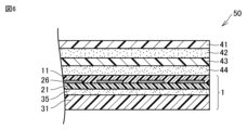
図6は、本実施形態の光学積層体50の一例を模式的に示す概略断面図である。図7は、本実施形態の光学積層体51の他の一例を模式的に示す概略断面図である。光学積層体50,51は、前面板41、円偏光板43、上記したTSパネルを有することができる。図6及び図7に示す光学積層体50,51は、図1に示すTSパネル1を備える場合を例に挙げているが、図2、図4又は図5に示すTSパネル2~4のうちのいずれかを備えていてもよい。
(ベース層)
ベース層30は、TS層20を支持するために用いられ、上記したように、例えば基材層31、第1貼合層35、及び支持層21を含むことができる。ベース層30の厚みDcやタフネスTcは、上記で説明したとおりであり、強度や取扱い性等の作業性、TSパネルの屈曲性等を考慮して設定すればよい。
基材層31は、支持層21に第1貼合層35を介して設けられ、TS層20に強度等を付与するために設けられる。基材層31は、温度40℃、湿度90%RHにおける透湿度が900g/(m2・24hr)以下であることが好ましく、500g/(m2・24hr)以下であることがより好ましく、300g/(m2・24hr)以下であることがさらに好ましく、200g/(m2・24hr)以下であることがよりさらに好ましく、100g/(m2・24hr)以下であってもよく、50g/(m2・24hr)以下であってもよい。基材層31の上記透湿度は、0g/(m2・24hr)超であってもよい。基材層31を形成する材料は、上記の透湿度を満たす材料であることが好ましく、TSパネルをフレキシブルディスプレイに適用する場合には特に、樹脂材料から形成されるフィルムであることが好ましい。
支持層21は、TS層20(パターン導電層(第1導電層及び第2導電層)、第2絶縁層)や第1絶縁層11を支持するための層である。支持層21は、分離層22、保護層23、屈折率調整層24、層間の密着性を向上するためのアンダーコート層、樹脂フィルム等を含むことができる。支持層21は、少なくとも分離層22を含むことが好ましい。支持層21は、通常、貼合層を有していない。
分離層22は、TS層20及び第1絶縁層11を製造する工程で用いる層であり、ガラス等のキャリア基板からの剥離のために用いられる層である。TS層20及び第1絶縁層11を製造する工程では、キャリア基板上に分離層22を形成し、この分離層22上にパターン導電層(第1導電層及び第2導電層)や第1絶縁層11を形成する。分離層22は、キャリア基板から、分離層22、パターン導電層(第1導電層及び第2導電層)、及び第1絶縁層11を剥離して分離するために用いられる。分離層22は、TS層20においてパターン導電層26や第1導電層27を被覆して保護する層として用いることができ、パターン導電層26や第1導電層27を電気的に絶縁させる機能を有していてもよい。
保護層23は、分離層22の第1絶縁層11側に設けることができ、分離層22に直接接するように設けることが好ましい。保護層23はパターニングされていてもよい。保護層23は、分離層22とともにパターン導電層26や第1導電層27を被覆して保護する層として用いることができる。保護層23は、パターン導電層26や第1導電層27を電気的に絶縁させる機能を有することができる。
屈折率調整層24は、TSパネルの屈折率を調整するための層であり、TSパネルに所定の屈折率を付与することができる。
支持層に用いることができる樹脂フィルムとしては、直線偏光層の片面又は両面に設けられる保護層の材料や、前面板をなす樹脂フィルムの材料と同じ材料を使用することができる。具体的には、ポリイミド、ポリアミド、ポリアミドイミド、環状ポリオレフィン系樹脂が好ましい。樹脂フィルムの厚みは、薄いことが好ましく、15μm以下であることができる。
第1貼合層35は、基材層31と支持層21とを貼合するための層である。第1貼合層35は、通常、基材層31及び支持層21に直接接するように設けられる。第1貼合層35は、接着剤組成物を用いて形成された接着剤層、又は、粘着剤組成物を用いて形成された粘着剤層である。第1貼合層35は接着剤層であることが好ましい。第1貼合層35は、低透湿性の材料から形成することが好ましい。
第1絶縁層11は、TS層20のパターン導電層26側や第2導電層28側に設けられて、パターン導電層26や第2導電層28を電気的に絶縁させる機能を有する。第1絶縁層11は、上記したように、温度40℃、湿度90%RHにおける透湿度Paが900g/(m2・24hr)以下であるものである。
TS層20は、上記したように、パターン導電層を有し、パターン導電層が積層方向に2層以上の導電層を有する場合、この導電層の間に存在する層(例えば、第2絶縁層29)を含む。
パターン導電層(第1導電層及び第2導電層である場合を含む)は、TSパネルにタッチされた位置を検出するための電極や配線であり、通常、パターン状に形成されている。パターン導電層は、図1に示すように単層構造や複数の層が互いに直接接する多層構造であってもよいが、図2に示すように2以上の導電層が積層方向に互いに離間して配置される積層構造を有していてもよい。
接続配線25(図2)は、外部回路や駆動回路と接続するための配線であり、通常表示領域の周囲に位置する第1導電層27上に設けられる。接続配線25は、単層構造であってもよく複数の層が互いに直接接する多層構造であってもよい。接続配線25の厚みは、0.01μm以上とすることができ、0.05μm以上であってもよく、0.1μm以上であってもよく、通常、5μm以下であり、1μm以下であることが好ましく、0.5μm以下であることがより好ましい。
第2絶縁層29は、パターン導電層をなす第1導電層27と第2導電層28との間に設けられ、第1導電層27と第2導電層28とを電気的に絶縁させる機能を有する。第2絶縁層29は、支持層21上に設けられた第1導電層27の支持層21とは反対側の表面を被覆し、面方向に離間する導電層の間の空間を埋めるように設けてもよい。第2絶縁層29の支持層21とは反対側には、第2導電層28が設けられる。第2絶縁層29には開口が設けられ、この開口にビア部を設けることにより、第1導電層27と第2導電層28とを電気的に接続することができる。
前面板41は、画像表示装置の表示素子等を保護するための層として機能することができ、光を透過可能な板状体であり、板状体は通常、樹脂製であることが好ましい。前面板41は、画像表示装置の最表面に配置されるものであることができる。前面板41は、樹脂フィルム、又は、樹脂フィルムの少なくとも一方の面にハードコート層を設けて硬度をより向上させたハードコート層付き樹脂フィルムであることが好ましい。また、前面板41は、ブルーライトカット機能、視野角調整機能等を有するものであってもよい。
円偏光板43は、直線偏光層及び位相差層を備えることができる。円偏光板43は、図6に示される光学積層体50において、直線偏光層が第2貼合層42側となり、位相差層が第3貼合層44側となるように配置される。すなわち、視認側から順に、直線偏光層と位相差層とが配置される。円偏光板43は、光学積層体50を有する画像表示装置の表示素子側から光学積層体50を通って出射される光を円偏光に変換することができる。また、円偏光板43は、外光の反射光の出射を抑制することができるため、光学積層体50に反射防止フィルムとしての機能を付与することができる。
直線偏光層は、自然光等の非偏光な光線からある一方向の直線偏光を選択的に透過させる機能を有するものである。直線偏光層は、吸収異方性を有する二色性色素を吸着させた延伸フィルムや、重合性液晶化合物の硬化物及び二色性色素を含み、二色性色素が、重合性液晶化合物の硬化物中に分散し、配向している液晶層等が挙げられる。二色性色素は、分子の長軸方向における吸光度と短軸方向における吸光度とが異なる性質を有する色素をいう。
吸収異方性を有する色素を吸着させた延伸フィルムは、通常、ポリビニルアルコール系樹脂フィルムを一軸延伸する工程、ポリビニルアルコール系樹脂フィルムを、ヨウ素等の二色性色素で染色することにより、その二色性色素を吸着させる工程、及び二色性色素が吸着されたポリビニルアルコール系樹脂フィルムをホウ酸水溶液で処理する工程を有する、及びホウ酸水溶液による処理後に水洗する工程を経て製造される。得られたフィルムをそのまま直線偏光層として用いてもよく、その片面又は両面に保護層を形成した直線偏光板として用いてもよい。こうして得られる直線偏光層の厚みは、好ましくは2μm~40μmである。
液晶層を形成するために用いる重合性液晶化合物は、重合性反応基を有し、かつ、液晶性を示す化合物である。重合性反応基は、重合反応に関与する基であり、光重合性反応基であることが好ましい。光重合性反応基は、光重合開始剤から発生した活性ラジカルや酸等によって重合反応に関与し得る基をいう。光重合性官能基としては、ビニル基、ビニルオキシ基、1-クロロビニル基、イソプロペニル基、4-ビニルフェニル基、アクリロイルオキシ基、メタクリロイルオキシ基、オキシラニル基、オキセタニル基等が挙げられる。中でも、アクリロイルオキシ基、メタクリロイルオキシ基、ビニルオキシ基、オキシラニル基及びオキセタニル基が好ましく、アクリロイルオキシ基がより好ましい。重合性液晶化合物の種類は特に限定されず、棒状液晶化合物、円盤状液晶化合物、及びこれらの混合物を用いることができる。重合性液晶化合物の液晶性は、サーモトロピック性液晶でもリオトロピック性液晶でもよく、相秩序構造としてはネマチック液晶でもスメクチック液晶でもよい。
位相差層は、1層であってもよく2層以上であってもよく、少なくともλ/4層を含む。λ/4層は、逆波長分散性であってもよい。位相差層表面を保護するオーバーコート層や、位相差層を支持する基材フィルムを有していてもよい。位相差層は、λ/4層を含み、さらに、λ/2層やポジティブC層を含んでいてもよい。位相差層がλ/2層を含む場合、直線偏光層側から順にλ/2層及びλ/4層を積層する。位相差層がポジティブC層を含む場合、直線偏光層側から順にλ/4層及びポジティブC層を積層してもよく、直線偏光板側から順にポジティブC層及びλ/4層を積層してもよい。
図6及び図7に示す光学積層体50,51で説明したように、第2貼合層42及び第3貼合層44は、前面板41と円偏光板43、前面板41とTSパネル、円偏光板43とTSパネルのいずれかを貼合するための層として用いることができる。第2貼合層42及び第3貼合層44は、それぞれ独立して、接着剤組成物を用いて形成された接着剤層、又は、粘着剤組成物を用いて形成された粘着剤層である。第2貼合層42及び第3貼合層44は、いずれも粘着剤層であることが好ましい。
(1) ベース層の透湿度Pcの測定
実施例及び比較例で用いたベース層の透湿度Pcの測定は、次の手順で行った。まず、実施例1に記載した手順で、ガラス基板上に分離層及び保護層を形成した後、ガラス基板を剥離し、この剥離によって露出した露出面と、各実施例及び各比較例で用いた基材層とを、各実施例及び各比較例で用いた紫外線硬化型の接着剤組成物を用いて貼合して第1貼合層を形成して、ベース層を作製した。作製したベース層を用いて、JIS Z 0208(カップ法)に準じた透湿度試験法により、測定温度40℃、測定湿度90%RH、測定時間24時間で、透湿度(水蒸気透過率)を測定した。
実施例及び比較例で用いた第1絶縁層の透湿度Paの測定は、次の手順で行った。第1絶縁層を形成するための組成物を、厚みが25μmのトリアセチルセルロース(TAC)フィルム上にコーティングし、乾燥後の厚みが表1に示すDaの厚みとなるようにフィルム状に形成し、測定用フィルムを得た。得られた測定用フィルムを用いて、上記(1)のベース層の透湿度Pcの測定で説明した透湿度試験法の手順にしたがい、透湿度を測定した。なお、TACフィルムの透湿度は、第1絶縁層の透湿度に比べて十分に大きいため、測定用サンプルを用いて測定された透湿度は、第1絶縁層の透湿度とみなすことができる。その結果を表1に示す。
ベース層の厚みDc及び第1絶縁層の厚みDaの測定は、カットした積層体の断面を透過型電子顕微鏡(SU8010、株式会社堀場製作所)を用いて観察し、得られた観察像から各層の厚みを測定した。実施例及び比較例において、第1絶縁層の厚みDa(第1絶縁層の最大厚み)は、図2にDaとして示す部分の厚みであった。測定された厚みの値を表1に示す。
ベース層のタフネスTcを測定するために、上記[透湿度の測定]の(1)ベース層の透湿度Pcの測定で説明した手順でベース層を作製した。作製したベース層のタフネスTcは、JIS K7161に準拠して、次のように測定した。ベース層から長辺110mm×短辺10mmの長方形の小片をスーパーカッターを用いて切り出した。次いで、引張試験機〔(株)島津製作所製 オートグラフ AG-Xplus試験機〕の上下つかみ具で、つかみ具の間隔が5cmとなるように上記小片の長辺方向両端を挟み、温度23℃、相対湿度55%の環境下、引張速度4mm/分で小片の長辺方向に引張った。タフネスは、初期から破断までの間における、応力-ひずみ曲線の積分値として算出した。その結果を表1に示す。
実施例及び比較例で得た光学積層体を、温度85℃、湿度85%RHの高温高湿環境下に24時間保管した。その後、温度25℃、湿度45%RHの常温環境下に30分間載置してから、TSパネルの駆動試験を行った。駆動試験は、TSパネルとタッチセンサ検査機とを接続し、タッチセンサ検査機でタッチセンサ機能を検査した。TS層中の各ノードにおいて静電容量を測定し、それらを平均して平均値を算出した。各ノードでの検出値が、すべてタッチセンサ機能が正常と判定される値の平均値の±15%以内であればAと評価した。各ノードにおける検出値が、一か所でも平均値+15%を超えたときは短絡(ショート)とみなし、一か所でも平均値-15%を下回ったときは開放(オープン)とみなしてBと評価した。
各実施例及び比較例で得たTSパネルの第1絶縁層側と、円偏光板のポジティブC層側とを、粘着剤層(8146-1、3M社製、厚み25μm)を介して貼合した視認性試験用積層体を、温度60℃、湿度90%RHの環境下に24時間保管した。その後、視認性試験用積層体を温度25℃、湿度45%RHの常温環境下に2時間載置してから、視認性試験を行った。視認性試験は、暗室で、LEDバックライト(DSN-1200、UP社製、照度3000Lux)の上に、LEDバックライト側にTSパネルが配置されるように視認性試験用積層体を置き、円偏光板側から肉眼で視認性試験用積層体を観察した。パターン導電層が視認されなかった場合をAと評価し、パターン導電層が視認された場合をBと評価した。その結果を表1に示す。
各実施例及び比較例で得た光学積層体のTSパネル側に、粘着剤層(8146-1、3M社製、厚み25μm)を介して、有機ELパネルを想定したパネル模写積層体を貼合して、屈曲性試験用積層体を得た。パネル模写積層体は、厚み38μmのポリイミド系樹脂フィルムPI1と、厚み50μmのポリイミド系樹脂フィルムPI2とを、粘着剤層(8146-1、3M社製、厚み25μm)を介して積層したものであり、ポリイミド系樹脂フィルムPI1側に光学積層体のTSパネルを貼合した。
屈曲回数が20万回に達してもみられない場合をA、
屈曲回数が10万回以上20万回未満でみられた場合をB、
屈曲回数が5万回以上10万回未満でみられた場合をC、
として屈曲性試験の評価を行った。
(1) TSパネルの作製
図5に示す構造を有するTSパネルを次の手順で準備した。キャリア基板としてのガラス基板に分離層、及び保護層をこの順に形成して支持層とし、保護層上に、図3に示すようなパターン状の単位パターン27a,27b(第1導電層)を形成した。分離層は、アクリル系樹脂組成物を用いてスロットダイコート法により形成した層であり、厚みは0.5μmであった。保護層は、アクリル系樹脂組成物を用いてスロットダイコート法により形成した層であり、厚みは3μmであった。第1導電層は、インジウムスズ酸化物(ITO)を用いてスパッタリングにより全面に膜を形成した後、フォトリソグラフィ法によりエッチングを行ってパターン状に形成した。第1導電層の厚みは0.1μmであった。第1導電層の単位セルの大きさは、図3に示すように、図3中の横方向の長さLwを4.2mmとし、縦方向の長さLlを4.3mmとした。また、単位パターン27a,27bとの間の距離d(図3)は10μmとした。第1導電層上の配線領域となる領域に、APC(Ag Palladium Copper合金)を用いてスパッタリングにより全面に膜を形成した後、フ
ォトリソグラフィ法によりエッチングを行ってパターン状に形成した。接続配線の厚み0.2μmの接続配線を形成した。
(前面板の準備)
前面板として、樹脂フィルムの両面にハードコート層が形成された厚み50μmのハードコート層付き樹脂フィルムを用意した。樹脂フィルムは、厚み30μmのポリアミドイミド(PAI)系樹脂フィルムであり、ハードコート層はそれぞれ、厚みが10μmであり、末端に多官能アクリル基を有するデンドリマー化合物を含む組成物から形成された層であった。
トリアセチルセルロース(TAC)フィルム(KC2UA、コニカミノルタ(株)社製、厚み25μm)に光配向膜を形成した後、二色性色素と重合性液晶化合物とを含む組成物を光配向膜上に塗布し、配向、硬化させて厚み2.5μmの直線偏光層を得た。この直線偏光層上に、オーバーコート層形成用組成物(水100部、ポリビニルアルコール樹脂粉末(KL318、(株)クラレ製、平均重合度18000)3部、架橋剤としてのポリアミドエポキシ樹脂(SR650(30)、住化ケムテックス(株)製)1.5部を混合したもの)を、乾燥後の厚みが1.0μmになるようにバーコート法により塗布してオーバーコート層を形成した。これにより、TACフィルム/光配向膜/直線偏光層/オーバーコート層の層構造を有する直線偏光板を得た。
上記で準備した前面板の一方の面に、第2貼合層としての粘着剤層(8146-1、3M社製、厚み25μm)を介して、円偏光板のTACフィルム側を貼合した。得られた積層体の円偏光板のポジティブC層側に、第3貼合層としての粘着剤層(8146-1、3M社製、厚み25μm)を介して、上記で作製したTSパネルの第1絶縁層を貼合して、図6に示す層構造の光学積層体を得た。前面板、第2貼合層、円偏光板、第3貼合層、及びTSパネルの貼合面には、貼合前にそれぞれコロナ処理を行った。得られた光学積層体は、縦165mm×横105mmであった。得られた光学積層体について、駆動試験及び屈曲性試験を行った。その結果を表1に示す。
基材層として、表1に示すものを用い、第1絶縁層の厚みを表1に示す厚みとしたこと以外は、実施例1と同様にしてTSパネルを作製した。作製したTSパネルを用いて、実施例1と同様の手順で光学積層体を得た。得られた光学積層体について、駆動試験及び屈曲性試験を行った。その結果を表1に示す。

Claims (9)
- ベース層、タッチセンサ層、及び第1絶縁層をこの順に有するタッチセンサパネルであって、
前記タッチセンサ層は、パターン導電層を有し、
前記第1絶縁層は、無機粒子を含まず、かつ、前記パターン導電層の前記ベース層側とは反対側の表面に直接接するように設けられ、
前記ベース層の温度40℃、湿度90%RHにおける透湿度Pcは、900g/(m2・24hr)以下であり、
前記第1絶縁層の温度40℃、湿度90%RHにおける透湿度Paは、900g/(m2・24hr)以下であり、
前記ベース層の厚みをDc[μm]とし、前記ベース層のタフネスをTc[mJ/mm3]とし、前記第1絶縁層の厚みをDa[μm]とするとき、下記式(1):
Tc/(Dc+Da)>0.03 (1)
[ここで、前記タフネスTcは、前記ベース層の長辺110mm×短辺10mmの長方形の小片を、引張試験機の上下つかみ具で、つかみ具の間隔が5cmとなるように長辺方向両端を挟み、温度23℃、相対湿度55%の環境下、引張速度4mm/分で前記小片を長辺方向に引張ったときの、初期から破断までの間における応力-ひずみ曲線の積分値として算出する。]
の関係を満たし、
前記タフネスTcは、200mJ/mm 3 以下である、タッチセンサパネル。 - 前記第1絶縁層は、前記タッチセンサ層の前記ベース層側とは反対側の表面を被覆し、かつ、前記パターン導電層の面方向に離間する導電部分の間の空間内にも設けられている、請求項1に記載のタッチセンサパネル。
- 前記パターン導電層は、前記ベース層側から順に第1導電層及び第2導電層を有し、
前記タッチセンサ層は、さらに、前記第1導電層と前記第2導電層との間に第2絶縁層を有する、請求項1又は2に記載のタッチセンサパネル。 - 前記ベース層は、前記タッチセンサ層側から順に、支持層、第1貼合層及び基材層を有する、請求項1~3のいずれか1項に記載のタッチセンサパネル。
- 前記支持層は、分離層を有する、請求項4に記載のタッチセンサパネル。
- 前記支持層は、さらに、前記分離層の前記タッチセンサ層側に保護層を有する、請求項5に記載のタッチセンサパネル。
- 前記支持層は、さらに、屈折率調整層を有する、請求項5又は6に記載のタッチセンサパネル。
- 前面板、円偏光板、及び、請求項1~7のいずれか1項に記載のタッチセンサパネルを有する、光学積層体。
- 前記前面板、第2貼合層、前記円偏光板、第3貼合層、及び前記タッチセンサパネルをこの順に有する、請求項8に記載の光学積層体。
Priority Applications (4)
| Application Number | Priority Date | Filing Date | Title |
|---|---|---|---|
| JP2019081086A JP7469852B2 (ja) | 2019-04-22 | 2019-04-22 | タッチセンサパネル及び光学積層体 |
| US16/853,037 US11822179B2 (en) | 2019-04-22 | 2020-04-20 | Touch sensor panel and optical laminate |
| CN202010311442.3A CN111831150A (zh) | 2019-04-22 | 2020-04-20 | 触摸传感器面板和光学层叠体 |
| KR1020200048773A KR20200123752A (ko) | 2019-04-22 | 2020-04-22 | 터치 센서 패널 및 광학 적층체 |
Applications Claiming Priority (1)
| Application Number | Priority Date | Filing Date | Title |
|---|---|---|---|
| JP2019081086A JP7469852B2 (ja) | 2019-04-22 | 2019-04-22 | タッチセンサパネル及び光学積層体 |
Publications (3)
| Publication Number | Publication Date |
|---|---|
| JP2020177570A JP2020177570A (ja) | 2020-10-29 |
| JP2020177570A5 JP2020177570A5 (ja) | 2022-03-25 |
| JP7469852B2 true JP7469852B2 (ja) | 2024-04-17 |
Family
ID=72832332
Family Applications (1)
| Application Number | Title | Priority Date | Filing Date |
|---|---|---|---|
| JP2019081086A Active JP7469852B2 (ja) | 2019-04-22 | 2019-04-22 | タッチセンサパネル及び光学積層体 |
Country Status (4)
| Country | Link |
|---|---|
| US (1) | US11822179B2 (ja) |
| JP (1) | JP7469852B2 (ja) |
| KR (1) | KR20200123752A (ja) |
| CN (1) | CN111831150A (ja) |
Families Citing this family (1)
| Publication number | Priority date | Publication date | Assignee | Title |
|---|---|---|---|---|
| US11789576B2 (en) * | 2021-11-16 | 2023-10-17 | Electronics And Telecommunications Research Institute | Flexible touch panel and method of manufacturing thereof |
Citations (7)
| Publication number | Priority date | Publication date | Assignee | Title |
|---|---|---|---|---|
| WO2015072321A1 (ja) | 2013-11-14 | 2015-05-21 | 旭硝子株式会社 | 透明導電性積層体およびタッチパネル |
| JP2017111567A (ja) | 2015-12-15 | 2017-06-22 | コニカミノルタ株式会社 | タッチパネル装置 |
| WO2017138611A1 (ja) | 2016-02-09 | 2017-08-17 | 大日本印刷株式会社 | 光学積層体及びその製造方法、前面板、並びに画像表示装置 |
| JP2018097869A (ja) | 2016-12-09 | 2018-06-21 | エルジー ディスプレイ カンパニー リミテッド | 電子機器 |
| JP2018116543A (ja) | 2017-01-19 | 2018-07-26 | 日東電工株式会社 | タッチパネル用フィルム積層体 |
| JP2018185811A (ja) | 2017-04-25 | 2018-11-22 | 東友ファインケム株式会社Dongwoo Fine−Chem Co., Ltd. | タッチセンサパネル |
| JP2019035801A (ja) | 2017-08-10 | 2019-03-07 | 日立化成株式会社 | 転写型感光性フィルム、硬化膜パターンの形成方法、硬化膜及び電子部品 |
Family Cites Families (14)
| Publication number | Priority date | Publication date | Assignee | Title |
|---|---|---|---|---|
| CN103238127A (zh) * | 2010-11-30 | 2013-08-07 | 日东电工株式会社 | 具有触摸输入功能的显示面板装置 |
| KR101933220B1 (ko) | 2011-07-07 | 2018-12-27 | 스미또모 가가꾸 가부시키가이샤 | 편광 소자, 원편광판 및 이들의 제조 방법 |
| JP6171276B2 (ja) | 2011-07-12 | 2017-08-02 | 住友化学株式会社 | 偏光子及びその製造方法 |
| WO2013084282A1 (ja) | 2011-12-05 | 2013-06-13 | 日立化成株式会社 | 樹脂硬化膜パターンの形成方法、感光性樹脂組成物及び感光性エレメント |
| JP2015069508A (ja) * | 2013-09-30 | 2015-04-13 | 凸版印刷株式会社 | タッチパネル |
| KR20150060536A (ko) | 2013-11-26 | 2015-06-03 | 삼성전기주식회사 | 터치센서 |
| TWI647532B (zh) | 2014-07-01 | 2019-01-11 | 南韓商東友精細化工有限公司 | 光敏樹脂組成物 |
| WO2016114074A1 (ja) * | 2015-01-15 | 2016-07-21 | コニカミノルタ株式会社 | 偏光板一体型タッチセンサー及びその製造方法 |
| TWI713619B (zh) | 2015-10-30 | 2020-12-21 | 日商住友化學股份有限公司 | 偏光板、具備該偏光板的顯示裝置,及其製造方法 |
| KR20170069123A (ko) * | 2015-12-10 | 2017-06-20 | 동우 화인켐 주식회사 | 터치 센서 및 그 제조방법 |
| WO2017187805A1 (ja) * | 2016-04-28 | 2017-11-02 | 富士フイルム株式会社 | タッチセンサー用導電シート、タッチセンサー用積層体、タッチセンサー、タッチパネル |
| JP6849346B2 (ja) | 2016-08-26 | 2021-03-24 | 三洋化成工業株式会社 | 感光性樹脂組成物 |
| JP6321108B2 (ja) * | 2016-10-04 | 2018-05-09 | 日東電工株式会社 | 光学積層体および画像表示装置 |
| KR20180097337A (ko) * | 2017-02-23 | 2018-08-31 | 동우 화인켐 주식회사 | 터치 센서 및 이를 포함하는 화상 표시 장치 |
-
2019
- 2019-04-22 JP JP2019081086A patent/JP7469852B2/ja active Active
-
2020
- 2020-04-20 US US16/853,037 patent/US11822179B2/en active Active
- 2020-04-20 CN CN202010311442.3A patent/CN111831150A/zh active Pending
- 2020-04-22 KR KR1020200048773A patent/KR20200123752A/ko active Search and Examination
Patent Citations (7)
| Publication number | Priority date | Publication date | Assignee | Title |
|---|---|---|---|---|
| WO2015072321A1 (ja) | 2013-11-14 | 2015-05-21 | 旭硝子株式会社 | 透明導電性積層体およびタッチパネル |
| JP2017111567A (ja) | 2015-12-15 | 2017-06-22 | コニカミノルタ株式会社 | タッチパネル装置 |
| WO2017138611A1 (ja) | 2016-02-09 | 2017-08-17 | 大日本印刷株式会社 | 光学積層体及びその製造方法、前面板、並びに画像表示装置 |
| JP2018097869A (ja) | 2016-12-09 | 2018-06-21 | エルジー ディスプレイ カンパニー リミテッド | 電子機器 |
| JP2018116543A (ja) | 2017-01-19 | 2018-07-26 | 日東電工株式会社 | タッチパネル用フィルム積層体 |
| JP2018185811A (ja) | 2017-04-25 | 2018-11-22 | 東友ファインケム株式会社Dongwoo Fine−Chem Co., Ltd. | タッチセンサパネル |
| JP2019035801A (ja) | 2017-08-10 | 2019-03-07 | 日立化成株式会社 | 転写型感光性フィルム、硬化膜パターンの形成方法、硬化膜及び電子部品 |
Also Published As
| Publication number | Publication date |
|---|---|
| CN111831150A (zh) | 2020-10-27 |
| US11822179B2 (en) | 2023-11-21 |
| KR20200123752A (ko) | 2020-10-30 |
| JP2020177570A (ja) | 2020-10-29 |
| US20200333661A1 (en) | 2020-10-22 |
Similar Documents
| Publication | Publication Date | Title |
|---|---|---|
| JP6945586B2 (ja) | 積層体、及び画像表示装置 | |
| TWI708826B (zh) | 撓性積層體及具備其的圖像顯示裝置 | |
| JP7469889B2 (ja) | 光学積層体、及び表示装置の製造方法 | |
| JP7300906B2 (ja) | 光学積層体及びそれを備えた画像表示装置 | |
| JP6735891B2 (ja) | フレキシブル積層体及びそれを備えた画像表示装置 | |
| JP7469852B2 (ja) | タッチセンサパネル及び光学積層体 | |
| WO2021085000A1 (ja) | 光学積層体及び表示装置 | |
| WO2020170726A1 (ja) | フレキシブル積層体、およびそれを備えた画像表示装置 | |
| JP2023003753A (ja) | 光学積層体及び表示装置 | |
| WO2021200365A1 (ja) | 積層体 | |
| JP6739601B1 (ja) | 光学積層体及び表示装置 | |
| WO2021149359A1 (ja) | 光学積層体及び表示装置 | |
| WO2021182056A1 (ja) | 光学積層体 | |
| WO2020162102A1 (ja) | 光学積層体及び表示装置 | |
| WO2021200364A1 (ja) | 積層体 | |
| JP2021162856A (ja) | 積層体 | |
| KR20220044412A (ko) | 플렉서블 적층체 | |
| JP2021152644A (ja) | フレキシブル積層体、およびそれを備えた画像表示装置 | |
| JP2021162855A (ja) | 積層体 | |
| JP2021152645A (ja) | フレキシブル積層体、およびそれを備えた画像表示装置 |
Legal Events
| Date | Code | Title | Description |
|---|---|---|---|
| A521 | Request for written amendment filed |
Free format text: JAPANESE INTERMEDIATE CODE: A523 Effective date: 20220316 |
|
| A621 | Written request for application examination |
Free format text: JAPANESE INTERMEDIATE CODE: A621 Effective date: 20220316 |
|
| A977 | Report on retrieval |
Free format text: JAPANESE INTERMEDIATE CODE: A971007 Effective date: 20221216 |
|
| A131 | Notification of reasons for refusal |
Free format text: JAPANESE INTERMEDIATE CODE: A131 Effective date: 20230110 |
|
| A521 | Request for written amendment filed |
Free format text: JAPANESE INTERMEDIATE CODE: A523 Effective date: 20230313 |
|
| A131 | Notification of reasons for refusal |
Free format text: JAPANESE INTERMEDIATE CODE: A131 Effective date: 20230613 |
|
| A521 | Request for written amendment filed |
Free format text: JAPANESE INTERMEDIATE CODE: A523 Effective date: 20230825 |
|
| A02 | Decision of refusal |
Free format text: JAPANESE INTERMEDIATE CODE: A02 Effective date: 20231003 |
|
| A711 | Notification of change in applicant |
Free format text: JAPANESE INTERMEDIATE CODE: A711 Effective date: 20231218 |
|
| A521 | Request for written amendment filed |
Free format text: JAPANESE INTERMEDIATE CODE: A821 Effective date: 20231218 |
|
| A521 | Request for written amendment filed |
Free format text: JAPANESE INTERMEDIATE CODE: A523 Effective date: 20240125 |
|
| A911 | Transfer to examiner for re-examination before appeal (zenchi) |
Free format text: JAPANESE INTERMEDIATE CODE: A911 Effective date: 20240202 |
|
| TRDD | Decision of grant or rejection written | ||
| A01 | Written decision to grant a patent or to grant a registration (utility model) |
Free format text: JAPANESE INTERMEDIATE CODE: A01 Effective date: 20240319 |
|
| A61 | First payment of annual fees (during grant procedure) |
Free format text: JAPANESE INTERMEDIATE CODE: A61 Effective date: 20240405 |
|
| R150 | Certificate of patent or registration of utility model |
Ref document number: 7469852 Country of ref document: JP Free format text: JAPANESE INTERMEDIATE CODE: R150 |