JP7413432B2 - センサ、測距装置 - Google Patents
センサ、測距装置 Download PDFInfo
- Publication number
- JP7413432B2 JP7413432B2 JP2022065820A JP2022065820A JP7413432B2 JP 7413432 B2 JP7413432 B2 JP 7413432B2 JP 2022065820 A JP2022065820 A JP 2022065820A JP 2022065820 A JP2022065820 A JP 2022065820A JP 7413432 B2 JP7413432 B2 JP 7413432B2
- Authority
- JP
- Japan
- Prior art keywords
- region
- wiring
- apd
- type semiconductor
- semiconductor region
- Prior art date
- Legal status (The legal status is an assumption and is not a legal conclusion. Google has not performed a legal analysis and makes no representation as to the accuracy of the status listed.)
- Active
Links
- 239000004065 semiconductor Substances 0.000 claims description 326
- 238000002955 isolation Methods 0.000 claims description 138
- 238000009825 accumulation Methods 0.000 claims description 129
- 238000000926 separation method Methods 0.000 claims description 90
- 229910052751 metal Inorganic materials 0.000 claims description 51
- 239000002184 metal Substances 0.000 claims description 51
- 239000000758 substrate Substances 0.000 claims description 47
- 239000012528 membrane Substances 0.000 claims description 2
- 239000011800 void material Substances 0.000 claims 2
- 230000002093 peripheral effect Effects 0.000 description 97
- 230000005684 electric field Effects 0.000 description 75
- 238000003384 imaging method Methods 0.000 description 40
- XUIMIQQOPSSXEZ-UHFFFAOYSA-N Silicon Chemical compound [Si] XUIMIQQOPSSXEZ-UHFFFAOYSA-N 0.000 description 37
- 229910052710 silicon Inorganic materials 0.000 description 37
- 239000010703 silicon Substances 0.000 description 37
- 238000010586 diagram Methods 0.000 description 35
- 238000001514 detection method Methods 0.000 description 26
- 230000015556 catabolic process Effects 0.000 description 25
- 230000000694 effects Effects 0.000 description 24
- 239000000463 material Substances 0.000 description 22
- 238000005516 engineering process Methods 0.000 description 21
- 239000002772 conduction electron Substances 0.000 description 19
- 239000000969 carrier Substances 0.000 description 18
- 238000000034 method Methods 0.000 description 18
- 238000003860 storage Methods 0.000 description 18
- 239000012535 impurity Substances 0.000 description 14
- 230000003287 optical effect Effects 0.000 description 14
- 238000005468 ion implantation Methods 0.000 description 12
- VYPSYNLAJGMNEJ-UHFFFAOYSA-N Silicium dioxide Chemical compound O=[Si]=O VYPSYNLAJGMNEJ-UHFFFAOYSA-N 0.000 description 11
- 230000000903 blocking effect Effects 0.000 description 9
- 238000004519 manufacturing process Methods 0.000 description 9
- 230000008569 process Effects 0.000 description 8
- 230000007246 mechanism Effects 0.000 description 7
- 239000010949 copper Substances 0.000 description 6
- 230000000149 penetrating effect Effects 0.000 description 6
- 229910052581 Si3N4 Inorganic materials 0.000 description 5
- 239000004020 conductor Substances 0.000 description 5
- 230000007423 decrease Effects 0.000 description 5
- 238000009792 diffusion process Methods 0.000 description 5
- 238000005036 potential barrier Methods 0.000 description 5
- 235000012239 silicon dioxide Nutrition 0.000 description 5
- 239000000377 silicon dioxide Substances 0.000 description 5
- HQVNEWCFYHHQES-UHFFFAOYSA-N silicon nitride Chemical compound N12[Si]34N5[Si]62N3[Si]51N64 HQVNEWCFYHHQES-UHFFFAOYSA-N 0.000 description 5
- IJGRMHOSHXDMSA-UHFFFAOYSA-N Atomic nitrogen Chemical compound N#N IJGRMHOSHXDMSA-UHFFFAOYSA-N 0.000 description 4
- 229910052782 aluminium Inorganic materials 0.000 description 4
- XAGFODPZIPBFFR-UHFFFAOYSA-N aluminium Chemical compound [Al] XAGFODPZIPBFFR-UHFFFAOYSA-N 0.000 description 4
- 230000015572 biosynthetic process Effects 0.000 description 4
- 230000006698 induction Effects 0.000 description 4
- 238000009413 insulation Methods 0.000 description 4
- RYGMFSIKBFXOCR-UHFFFAOYSA-N Copper Chemical compound [Cu] RYGMFSIKBFXOCR-UHFFFAOYSA-N 0.000 description 3
- 230000005540 biological transmission Effects 0.000 description 3
- 230000008859 change Effects 0.000 description 3
- 238000006243 chemical reaction Methods 0.000 description 3
- 229910052681 coesite Inorganic materials 0.000 description 3
- 229910052802 copper Inorganic materials 0.000 description 3
- 229910052906 cristobalite Inorganic materials 0.000 description 3
- 238000007667 floating Methods 0.000 description 3
- 238000012545 processing Methods 0.000 description 3
- 229910052682 stishovite Inorganic materials 0.000 description 3
- 229910052905 tridymite Inorganic materials 0.000 description 3
- 229910052721 tungsten Inorganic materials 0.000 description 3
- 239000010937 tungsten Substances 0.000 description 3
- NRTOMJZYCJJWKI-UHFFFAOYSA-N Titanium nitride Chemical compound [Ti]#N NRTOMJZYCJJWKI-UHFFFAOYSA-N 0.000 description 2
- 230000001133 acceleration Effects 0.000 description 2
- 238000000231 atomic layer deposition Methods 0.000 description 2
- 229910000420 cerium oxide Inorganic materials 0.000 description 2
- 230000007547 defect Effects 0.000 description 2
- 230000002542 deteriorative effect Effects 0.000 description 2
- 229910003440 dysprosium oxide Inorganic materials 0.000 description 2
- NLQFUUYNQFMIJW-UHFFFAOYSA-N dysprosium(iii) oxide Chemical compound O=[Dy]O[Dy]=O NLQFUUYNQFMIJW-UHFFFAOYSA-N 0.000 description 2
- 229910001940 europium oxide Inorganic materials 0.000 description 2
- AEBZCFFCDTZXHP-UHFFFAOYSA-N europium(3+);oxygen(2-) Chemical compound [O-2].[O-2].[O-2].[Eu+3].[Eu+3] AEBZCFFCDTZXHP-UHFFFAOYSA-N 0.000 description 2
- 229910052735 hafnium Inorganic materials 0.000 description 2
- -1 hafnium nitride Chemical class 0.000 description 2
- 230000001939 inductive effect Effects 0.000 description 2
- 238000009434 installation Methods 0.000 description 2
- 239000011810 insulating material Substances 0.000 description 2
- 229910003443 lutetium oxide Inorganic materials 0.000 description 2
- 150000004767 nitrides Chemical class 0.000 description 2
- 229910052757 nitrogen Inorganic materials 0.000 description 2
- TWNQGVIAIRXVLR-UHFFFAOYSA-N oxo(oxoalumanyloxy)alumane Chemical compound O=[Al]O[Al]=O TWNQGVIAIRXVLR-UHFFFAOYSA-N 0.000 description 2
- BMMGVYCKOGBVEV-UHFFFAOYSA-N oxo(oxoceriooxy)cerium Chemical compound [Ce]=O.O=[Ce]=O BMMGVYCKOGBVEV-UHFFFAOYSA-N 0.000 description 2
- MPARYNQUYZOBJM-UHFFFAOYSA-N oxo(oxolutetiooxy)lutetium Chemical compound O=[Lu]O[Lu]=O MPARYNQUYZOBJM-UHFFFAOYSA-N 0.000 description 2
- SIWVEOZUMHYXCS-UHFFFAOYSA-N oxo(oxoyttriooxy)yttrium Chemical compound O=[Y]O[Y]=O SIWVEOZUMHYXCS-UHFFFAOYSA-N 0.000 description 2
- RVTZCBVAJQQJTK-UHFFFAOYSA-N oxygen(2-);zirconium(4+) Chemical compound [O-2].[O-2].[Zr+4] RVTZCBVAJQQJTK-UHFFFAOYSA-N 0.000 description 2
- 229910021420 polycrystalline silicon Inorganic materials 0.000 description 2
- 229920005591 polysilicon Polymers 0.000 description 2
- MZLGASXMSKOWSE-UHFFFAOYSA-N tantalum nitride Chemical compound [Ta]#N MZLGASXMSKOWSE-UHFFFAOYSA-N 0.000 description 2
- 239000010936 titanium Substances 0.000 description 2
- WFKWXMTUELFFGS-UHFFFAOYSA-N tungsten Chemical compound [W] WFKWXMTUELFFGS-UHFFFAOYSA-N 0.000 description 2
- 229910001928 zirconium oxide Inorganic materials 0.000 description 2
- 101100207343 Antirrhinum majus 1e20 gene Proteins 0.000 description 1
- GWEVSGVZZGPLCZ-UHFFFAOYSA-N Titan oxide Chemical compound O=[Ti]=O GWEVSGVZZGPLCZ-UHFFFAOYSA-N 0.000 description 1
- RTAQQCXQSZGOHL-UHFFFAOYSA-N Titanium Chemical compound [Ti] RTAQQCXQSZGOHL-UHFFFAOYSA-N 0.000 description 1
- UPEMFLOMQVFMCZ-UHFFFAOYSA-N [O--].[O--].[O--].[Pm+3].[Pm+3] Chemical compound [O--].[O--].[O--].[Pm+3].[Pm+3] UPEMFLOMQVFMCZ-UHFFFAOYSA-N 0.000 description 1
- 230000001154 acute effect Effects 0.000 description 1
- 230000003321 amplification Effects 0.000 description 1
- 238000005229 chemical vapour deposition Methods 0.000 description 1
- 239000003086 colorant Substances 0.000 description 1
- 238000002485 combustion reaction Methods 0.000 description 1
- 238000004891 communication Methods 0.000 description 1
- PMHQVHHXPFUNSP-UHFFFAOYSA-M copper(1+);methylsulfanylmethane;bromide Chemical compound Br[Cu].CSC PMHQVHHXPFUNSP-UHFFFAOYSA-M 0.000 description 1
- 230000003247 decreasing effect Effects 0.000 description 1
- 230000006866 deterioration Effects 0.000 description 1
- ZXGIFJXRQHZCGJ-UHFFFAOYSA-N erbium(3+);oxygen(2-) Chemical compound [O-2].[O-2].[O-2].[Er+3].[Er+3] ZXGIFJXRQHZCGJ-UHFFFAOYSA-N 0.000 description 1
- 230000005669 field effect Effects 0.000 description 1
- CMIHHWBVHJVIGI-UHFFFAOYSA-N gadolinium(iii) oxide Chemical compound [O-2].[O-2].[O-2].[Gd+3].[Gd+3] CMIHHWBVHJVIGI-UHFFFAOYSA-N 0.000 description 1
- 230000004313 glare Effects 0.000 description 1
- VBJZVLUMGGDVMO-UHFFFAOYSA-N hafnium atom Chemical compound [Hf] VBJZVLUMGGDVMO-UHFFFAOYSA-N 0.000 description 1
- CJNBYAVZURUTKZ-UHFFFAOYSA-N hafnium(iv) oxide Chemical compound O=[Hf]=O CJNBYAVZURUTKZ-UHFFFAOYSA-N 0.000 description 1
- OWCYYNSBGXMRQN-UHFFFAOYSA-N holmium(3+);oxygen(2-) Chemical compound [O-2].[O-2].[O-2].[Ho+3].[Ho+3] OWCYYNSBGXMRQN-UHFFFAOYSA-N 0.000 description 1
- 230000001771 impaired effect Effects 0.000 description 1
- MRELNEQAGSRDBK-UHFFFAOYSA-N lanthanum(3+);oxygen(2-) Chemical compound [O-2].[O-2].[O-2].[La+3].[La+3] MRELNEQAGSRDBK-UHFFFAOYSA-N 0.000 description 1
- 230000000670 limiting effect Effects 0.000 description 1
- 238000012423 maintenance Methods 0.000 description 1
- 238000005259 measurement Methods 0.000 description 1
- 239000007769 metal material Substances 0.000 description 1
- 150000002739 metals Chemical class 0.000 description 1
- 230000000116 mitigating effect Effects 0.000 description 1
- PLDDOISOJJCEMH-UHFFFAOYSA-N neodymium(3+);oxygen(2-) Chemical compound [O-2].[O-2].[O-2].[Nd+3].[Nd+3] PLDDOISOJJCEMH-UHFFFAOYSA-N 0.000 description 1
- 238000003199 nucleic acid amplification method Methods 0.000 description 1
- 230000001151 other effect Effects 0.000 description 1
- MMKQUGHLEMYQSG-UHFFFAOYSA-N oxygen(2-);praseodymium(3+) Chemical compound [O-2].[O-2].[O-2].[Pr+3].[Pr+3] MMKQUGHLEMYQSG-UHFFFAOYSA-N 0.000 description 1
- BPUBBGLMJRNUCC-UHFFFAOYSA-N oxygen(2-);tantalum(5+) Chemical compound [O-2].[O-2].[O-2].[O-2].[O-2].[Ta+5].[Ta+5] BPUBBGLMJRNUCC-UHFFFAOYSA-N 0.000 description 1
- UZLYXNNZYFBAQO-UHFFFAOYSA-N oxygen(2-);ytterbium(3+) Chemical compound [O-2].[O-2].[O-2].[Yb+3].[Yb+3] UZLYXNNZYFBAQO-UHFFFAOYSA-N 0.000 description 1
- 239000012071 phase Substances 0.000 description 1
- 238000005268 plasma chemical vapour deposition Methods 0.000 description 1
- 238000002294 plasma sputter deposition Methods 0.000 description 1
- 238000005498 polishing Methods 0.000 description 1
- 230000002265 prevention Effects 0.000 description 1
- FKTOIHSPIPYAPE-UHFFFAOYSA-N samarium(iii) oxide Chemical compound [O-2].[O-2].[O-2].[Sm+3].[Sm+3] FKTOIHSPIPYAPE-UHFFFAOYSA-N 0.000 description 1
- 230000035945 sensitivity Effects 0.000 description 1
- 229910052814 silicon oxide Inorganic materials 0.000 description 1
- 238000009751 slip forming Methods 0.000 description 1
- 239000007790 solid phase Substances 0.000 description 1
- 238000004544 sputter deposition Methods 0.000 description 1
- 229910052715 tantalum Inorganic materials 0.000 description 1
- GUVRBAGPIYLISA-UHFFFAOYSA-N tantalum atom Chemical compound [Ta] GUVRBAGPIYLISA-UHFFFAOYSA-N 0.000 description 1
- 230000002123 temporal effect Effects 0.000 description 1
- SCRZPWWVSXWCMC-UHFFFAOYSA-N terbium(iii) oxide Chemical compound [O-2].[O-2].[O-2].[Tb+3].[Tb+3] SCRZPWWVSXWCMC-UHFFFAOYSA-N 0.000 description 1
- ZIKATJAYWZUJPY-UHFFFAOYSA-N thulium(iii) oxide Chemical compound [O-2].[O-2].[O-2].[Tm+3].[Tm+3] ZIKATJAYWZUJPY-UHFFFAOYSA-N 0.000 description 1
- 229910052719 titanium Inorganic materials 0.000 description 1
Images


Classifications
-
- H—ELECTRICITY
- H01—ELECTRIC ELEMENTS
- H01L—SEMICONDUCTOR DEVICES NOT COVERED BY CLASS H10
- H01L27/00—Devices consisting of a plurality of semiconductor or other solid-state components formed in or on a common substrate
- H01L27/14—Devices consisting of a plurality of semiconductor or other solid-state components formed in or on a common substrate including semiconductor components sensitive to infrared radiation, light, electromagnetic radiation of shorter wavelength or corpuscular radiation and specially adapted either for the conversion of the energy of such radiation into electrical energy or for the control of electrical energy by such radiation
- H01L27/144—Devices controlled by radiation
- H01L27/146—Imager structures
- H01L27/14601—Structural or functional details thereof
- H01L27/1463—Pixel isolation structures
-
- H—ELECTRICITY
- H01—ELECTRIC ELEMENTS
- H01L—SEMICONDUCTOR DEVICES NOT COVERED BY CLASS H10
- H01L27/00—Devices consisting of a plurality of semiconductor or other solid-state components formed in or on a common substrate
- H01L27/14—Devices consisting of a plurality of semiconductor or other solid-state components formed in or on a common substrate including semiconductor components sensitive to infrared radiation, light, electromagnetic radiation of shorter wavelength or corpuscular radiation and specially adapted either for the conversion of the energy of such radiation into electrical energy or for the control of electrical energy by such radiation
- H01L27/144—Devices controlled by radiation
- H01L27/146—Imager structures
- H01L27/14601—Structural or functional details thereof
- H01L27/14609—Pixel-elements with integrated switching, control, storage or amplification elements
-
- H—ELECTRICITY
- H01—ELECTRIC ELEMENTS
- H01L—SEMICONDUCTOR DEVICES NOT COVERED BY CLASS H10
- H01L27/00—Devices consisting of a plurality of semiconductor or other solid-state components formed in or on a common substrate
- H01L27/14—Devices consisting of a plurality of semiconductor or other solid-state components formed in or on a common substrate including semiconductor components sensitive to infrared radiation, light, electromagnetic radiation of shorter wavelength or corpuscular radiation and specially adapted either for the conversion of the energy of such radiation into electrical energy or for the control of electrical energy by such radiation
- H01L27/144—Devices controlled by radiation
- H01L27/146—Imager structures
- H01L27/14601—Structural or functional details thereof
- H01L27/14603—Special geometry or disposition of pixel-elements, address-lines or gate-electrodes
- H01L27/14605—Structural or functional details relating to the position of the pixel elements, e.g. smaller pixel elements in the center of the imager compared to pixel elements at the periphery
-
- H—ELECTRICITY
- H01—ELECTRIC ELEMENTS
- H01L—SEMICONDUCTOR DEVICES NOT COVERED BY CLASS H10
- H01L27/00—Devices consisting of a plurality of semiconductor or other solid-state components formed in or on a common substrate
- H01L27/14—Devices consisting of a plurality of semiconductor or other solid-state components formed in or on a common substrate including semiconductor components sensitive to infrared radiation, light, electromagnetic radiation of shorter wavelength or corpuscular radiation and specially adapted either for the conversion of the energy of such radiation into electrical energy or for the control of electrical energy by such radiation
- H01L27/144—Devices controlled by radiation
- H01L27/146—Imager structures
- H01L27/14601—Structural or functional details thereof
- H01L27/14603—Special geometry or disposition of pixel-elements, address-lines or gate-electrodes
- H01L27/14607—Geometry of the photosensitive area
-
- H—ELECTRICITY
- H01—ELECTRIC ELEMENTS
- H01L—SEMICONDUCTOR DEVICES NOT COVERED BY CLASS H10
- H01L27/00—Devices consisting of a plurality of semiconductor or other solid-state components formed in or on a common substrate
- H01L27/14—Devices consisting of a plurality of semiconductor or other solid-state components formed in or on a common substrate including semiconductor components sensitive to infrared radiation, light, electromagnetic radiation of shorter wavelength or corpuscular radiation and specially adapted either for the conversion of the energy of such radiation into electrical energy or for the control of electrical energy by such radiation
- H01L27/144—Devices controlled by radiation
- H01L27/146—Imager structures
- H01L27/14601—Structural or functional details thereof
- H01L27/14609—Pixel-elements with integrated switching, control, storage or amplification elements
- H01L27/1461—Pixel-elements with integrated switching, control, storage or amplification elements characterised by the photosensitive area
-
- H—ELECTRICITY
- H01—ELECTRIC ELEMENTS
- H01L—SEMICONDUCTOR DEVICES NOT COVERED BY CLASS H10
- H01L27/00—Devices consisting of a plurality of semiconductor or other solid-state components formed in or on a common substrate
- H01L27/14—Devices consisting of a plurality of semiconductor or other solid-state components formed in or on a common substrate including semiconductor components sensitive to infrared radiation, light, electromagnetic radiation of shorter wavelength or corpuscular radiation and specially adapted either for the conversion of the energy of such radiation into electrical energy or for the control of electrical energy by such radiation
- H01L27/144—Devices controlled by radiation
- H01L27/146—Imager structures
- H01L27/14601—Structural or functional details thereof
- H01L27/1462—Coatings
- H01L27/14623—Optical shielding
-
- H—ELECTRICITY
- H01—ELECTRIC ELEMENTS
- H01L—SEMICONDUCTOR DEVICES NOT COVERED BY CLASS H10
- H01L27/00—Devices consisting of a plurality of semiconductor or other solid-state components formed in or on a common substrate
- H01L27/14—Devices consisting of a plurality of semiconductor or other solid-state components formed in or on a common substrate including semiconductor components sensitive to infrared radiation, light, electromagnetic radiation of shorter wavelength or corpuscular radiation and specially adapted either for the conversion of the energy of such radiation into electrical energy or for the control of electrical energy by such radiation
- H01L27/144—Devices controlled by radiation
- H01L27/146—Imager structures
- H01L27/14601—Structural or functional details thereof
- H01L27/14625—Optical elements or arrangements associated with the device
- H01L27/14627—Microlenses
-
- H—ELECTRICITY
- H01—ELECTRIC ELEMENTS
- H01L—SEMICONDUCTOR DEVICES NOT COVERED BY CLASS H10
- H01L27/00—Devices consisting of a plurality of semiconductor or other solid-state components formed in or on a common substrate
- H01L27/14—Devices consisting of a plurality of semiconductor or other solid-state components formed in or on a common substrate including semiconductor components sensitive to infrared radiation, light, electromagnetic radiation of shorter wavelength or corpuscular radiation and specially adapted either for the conversion of the energy of such radiation into electrical energy or for the control of electrical energy by such radiation
- H01L27/144—Devices controlled by radiation
- H01L27/146—Imager structures
- H01L27/14601—Structural or functional details thereof
- H01L27/14634—Assemblies, i.e. Hybrid structures
-
- H—ELECTRICITY
- H01—ELECTRIC ELEMENTS
- H01L—SEMICONDUCTOR DEVICES NOT COVERED BY CLASS H10
- H01L27/00—Devices consisting of a plurality of semiconductor or other solid-state components formed in or on a common substrate
- H01L27/14—Devices consisting of a plurality of semiconductor or other solid-state components formed in or on a common substrate including semiconductor components sensitive to infrared radiation, light, electromagnetic radiation of shorter wavelength or corpuscular radiation and specially adapted either for the conversion of the energy of such radiation into electrical energy or for the control of electrical energy by such radiation
- H01L27/144—Devices controlled by radiation
- H01L27/146—Imager structures
- H01L27/14601—Structural or functional details thereof
- H01L27/14636—Interconnect structures
-
- H—ELECTRICITY
- H01—ELECTRIC ELEMENTS
- H01L—SEMICONDUCTOR DEVICES NOT COVERED BY CLASS H10
- H01L27/00—Devices consisting of a plurality of semiconductor or other solid-state components formed in or on a common substrate
- H01L27/14—Devices consisting of a plurality of semiconductor or other solid-state components formed in or on a common substrate including semiconductor components sensitive to infrared radiation, light, electromagnetic radiation of shorter wavelength or corpuscular radiation and specially adapted either for the conversion of the energy of such radiation into electrical energy or for the control of electrical energy by such radiation
- H01L27/144—Devices controlled by radiation
- H01L27/146—Imager structures
- H01L27/14601—Structural or functional details thereof
- H01L27/1464—Back illuminated imager structures
-
- H—ELECTRICITY
- H01—ELECTRIC ELEMENTS
- H01L—SEMICONDUCTOR DEVICES NOT COVERED BY CLASS H10
- H01L27/00—Devices consisting of a plurality of semiconductor or other solid-state components formed in or on a common substrate
- H01L27/14—Devices consisting of a plurality of semiconductor or other solid-state components formed in or on a common substrate including semiconductor components sensitive to infrared radiation, light, electromagnetic radiation of shorter wavelength or corpuscular radiation and specially adapted either for the conversion of the energy of such radiation into electrical energy or for the control of electrical energy by such radiation
- H01L27/144—Devices controlled by radiation
- H01L27/146—Imager structures
- H01L27/14643—Photodiode arrays; MOS imagers
-
- H—ELECTRICITY
- H01—ELECTRIC ELEMENTS
- H01L—SEMICONDUCTOR DEVICES NOT COVERED BY CLASS H10
- H01L27/00—Devices consisting of a plurality of semiconductor or other solid-state components formed in or on a common substrate
- H01L27/14—Devices consisting of a plurality of semiconductor or other solid-state components formed in or on a common substrate including semiconductor components sensitive to infrared radiation, light, electromagnetic radiation of shorter wavelength or corpuscular radiation and specially adapted either for the conversion of the energy of such radiation into electrical energy or for the control of electrical energy by such radiation
- H01L27/144—Devices controlled by radiation
- H01L27/146—Imager structures
- H01L27/14683—Processes or apparatus peculiar to the manufacture or treatment of these devices or parts thereof
- H01L27/1469—Assemblies, i.e. hybrid integration
-
- H—ELECTRICITY
- H01—ELECTRIC ELEMENTS
- H01L—SEMICONDUCTOR DEVICES NOT COVERED BY CLASS H10
- H01L31/00—Semiconductor devices sensitive to infrared radiation, light, electromagnetic radiation of shorter wavelength or corpuscular radiation and specially adapted either for the conversion of the energy of such radiation into electrical energy or for the control of electrical energy by such radiation; Processes or apparatus specially adapted for the manufacture or treatment thereof or of parts thereof; Details thereof
- H01L31/02—Details
- H01L31/0216—Coatings
- H01L31/02161—Coatings for devices characterised by at least one potential jump barrier or surface barrier
- H01L31/02162—Coatings for devices characterised by at least one potential jump barrier or surface barrier for filtering or shielding light, e.g. multicolour filters for photodetectors
-
- H—ELECTRICITY
- H01—ELECTRIC ELEMENTS
- H01L—SEMICONDUCTOR DEVICES NOT COVERED BY CLASS H10
- H01L31/00—Semiconductor devices sensitive to infrared radiation, light, electromagnetic radiation of shorter wavelength or corpuscular radiation and specially adapted either for the conversion of the energy of such radiation into electrical energy or for the control of electrical energy by such radiation; Processes or apparatus specially adapted for the manufacture or treatment thereof or of parts thereof; Details thereof
- H01L31/02—Details
- H01L31/0232—Optical elements or arrangements associated with the device
- H01L31/02327—Optical elements or arrangements associated with the device the optical elements being integrated or being directly associated to the device, e.g. back reflectors
-
- H—ELECTRICITY
- H01—ELECTRIC ELEMENTS
- H01L—SEMICONDUCTOR DEVICES NOT COVERED BY CLASS H10
- H01L31/00—Semiconductor devices sensitive to infrared radiation, light, electromagnetic radiation of shorter wavelength or corpuscular radiation and specially adapted either for the conversion of the energy of such radiation into electrical energy or for the control of electrical energy by such radiation; Processes or apparatus specially adapted for the manufacture or treatment thereof or of parts thereof; Details thereof
- H01L31/08—Semiconductor devices sensitive to infrared radiation, light, electromagnetic radiation of shorter wavelength or corpuscular radiation and specially adapted either for the conversion of the energy of such radiation into electrical energy or for the control of electrical energy by such radiation; Processes or apparatus specially adapted for the manufacture or treatment thereof or of parts thereof; Details thereof in which radiation controls flow of current through the device, e.g. photoresistors
- H01L31/10—Semiconductor devices sensitive to infrared radiation, light, electromagnetic radiation of shorter wavelength or corpuscular radiation and specially adapted either for the conversion of the energy of such radiation into electrical energy or for the control of electrical energy by such radiation; Processes or apparatus specially adapted for the manufacture or treatment thereof or of parts thereof; Details thereof in which radiation controls flow of current through the device, e.g. photoresistors characterised by at least one potential-jump barrier or surface barrier, e.g. phototransistors
- H01L31/101—Devices sensitive to infrared, visible or ultraviolet radiation
- H01L31/102—Devices sensitive to infrared, visible or ultraviolet radiation characterised by only one potential barrier or surface barrier
- H01L31/107—Devices sensitive to infrared, visible or ultraviolet radiation characterised by only one potential barrier or surface barrier the potential barrier working in avalanche mode, e.g. avalanche photodiode
-
- H—ELECTRICITY
- H01—ELECTRIC ELEMENTS
- H01L—SEMICONDUCTOR DEVICES NOT COVERED BY CLASS H10
- H01L27/00—Devices consisting of a plurality of semiconductor or other solid-state components formed in or on a common substrate
- H01L27/14—Devices consisting of a plurality of semiconductor or other solid-state components formed in or on a common substrate including semiconductor components sensitive to infrared radiation, light, electromagnetic radiation of shorter wavelength or corpuscular radiation and specially adapted either for the conversion of the energy of such radiation into electrical energy or for the control of electrical energy by such radiation
- H01L27/144—Devices controlled by radiation
- H01L27/146—Imager structures
- H01L27/14601—Structural or functional details thereof
- H01L27/14609—Pixel-elements with integrated switching, control, storage or amplification elements
- H01L27/14612—Pixel-elements with integrated switching, control, storage or amplification elements involving a transistor
Description
ガイガーモードのアバランシェフォトダイオードは、シングルフォトンアバランシェダイオード(SPAD)とも呼ばれている。
図1は、表面照射型のAPDの構成を示す図である。画素10は、図中下側から参照するに、APD21上に配線層22が積層され、配線層22上にオンチップレンズ23が積層されている。APD21の詳細な構成については後述する。
図2は、裏面照射型の画素の構成を示す図である。画素30は、図中下側から参照するに、オンチップレンズ23上にAPD21が積層され、APD21上にセンサ基板41が積層され、さらにセンサ基板41上に回路基板42が積層された構成とされている。
図3は、APD21の第1の実施の形態における断面構成を示す図である。図3に示すように、APD21aには、導電型がn型(第1導電型)のn型半導体領域101と、n型半導体領域101の下部に導電型がp型(第2導電型)のp型半導体領域102が形成されている。n型半導体領域101とp型半導体領域102は、ウェル層103内に形成されている。
また、ここでは、ホール蓄積領域107aと記載し、ホールを蓄積し、電子をトラップする場合を例に挙げて説明しているが、第10の実施の形態として説明するAPD21j(図23)のように、電子を蓄積し、ホールをトラップさせる構成とすることもでき、ホールをトラップさせるように構成した場合も、DCRを抑制することができる。
図6は、APD21の第2の実施の形態における断面構成を示す図である。図6に示したAPD21bにおいて、図3に示したAPD21aと同様の部分については同一の符号を付し、その説明は省略する。
また、APD21bも、APD21a(図3)と同じく、ホール蓄積領域107bは、アノード105の下部に形成され、アノード105が、分離領域108の内部に連続的にウェル層103を囲むように形成されているのと同じく、ホール蓄積領域107bも、分離領域108の内部に連続的にウェル層103を囲むように形成されている。
図7は、APD21の第3の実施の形態における断面構成を示す図である。図7に示したAPD21cにおいて、図3に示したAPD21aと同様の部分については同一の符号を付し、その説明は省略する。
図9は、APD21の第4の実施の形態における断面構成を示す図である。図9に示したAPD21dにおいて、図3に示したAPD21aと同様の部分については同一の符号を付し、その説明は省略する。
図12は、APD21の第5の実施の形態における断面構成を示す図である。図12に示したAPD21eにおいて、図3に示したAPD21aと同様の部分については同一の符号を付し、その説明は省略する。
図15は、APD21の第6の実施の形態における断面構成を示す図である。図15に示したAPD21fにおいて、図3に示したAPD21aと同様の部分については同一の符号を付し、その説明は省略する。
図17は、APD21の第7の実施の形態における平面構成を示す図である。図17に示したAPD21gにおいて、図4に示したAPD21aと同様の部分については同一の符号を付し、その説明は省略する。
図19は、APD21の第8の実施の形態における断面構成を示す図である。図19に示したAPD21hにおいて、図3に示したAPD21aと同様の部分については同一の符号を付し、その説明は省略する。
図21は、APD21の第9の実施の形態における断面構成を示す図である。図21に示したAPD21iにおいて、図3に示したAPD21aと同様の部分については同一の符号を付し、その説明は省略する。
図23は、APD21の第10の実施の形態における断面構成を示す図である。図23に示したAPD21jは、第1乃至第9の実施の形態におけるAPD21と異なる極性を有している点が異なるが、構成は同一である。
また電子蓄積領域107jは、ウェル層103jと分離領域108との間と、ウェル層103jの下部(APD21jの裏面側)に形成されている。
図25は、APD21の第11の実施の形態における断面構成を示す図である。図25に示したAPD21kは、第1乃至第10の実施の形態におけるAPD21と基本的な構成は同一であるが、PDEの低下や、暗信号の増加を発生させることなく、エッジブレイクダウンを防ぐことができる構成を有している点で異なる。
またブロック層301を、p型半導体領域102の端部の近傍に形成することで、より多くの伝導電子311を増倍領域に導くことが可能となり、PDEを向上させることが可能となる。
図31は、APD21の第12の実施の形態における断面構成を示す図である。図31に示したAPD21mは、第1乃の実施の形態におけるAPD21と構成は基本的に同一であるが、PDEの低下や、暗信号の増加を発生させることなく、エッジブレイクダウンを防ぐことができる構成を有している点で異なる。
なお、図示はしないが、第11の実施の形態におけるAPD21kと同じく、第12の実施の形態におけるAPD21mを、分離領域108を削除した構成とすることもできる。
なお、図示はしないが、第11の実施の形態におけるAPD21kと同じく、第12の実施の形態におけるAPD21mを、ホール蓄積領域107mと分離領域108を削除した構成とすることもできる。
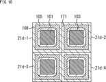
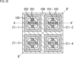
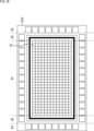
上記した実施の形態においては、APD21について説明した。APD21は、図35、図36に示すように、センサチップ310に設けられている画素領域A1にアレイ状に配置されている。図36では、APD21-1とAPD21-2が画素領域A1に並んで配置されている例を示した。
このトレンチ323については、図51以降を参照して後述する。
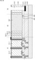
APD21には、APD21間を分離するための分離領域が形成されている。例えば、図3に示したAPD21aでは、分離領域108が形成されている。
分離領域の第2の実施の形態について、図39を参照して説明する。上記した分離領域の第1の実施の形態における分離領域108aは、遮光膜402を、p型半導体領域415とトレンチ412を接続する配線として用いる場合を例に挙げて説明したが、分離領域の第2の実施の形態における分離領域108bは、配線を形成し、p型半導体領域415とトレンチ412を接続する構成とされている点が、分離領域の第1の実施形態における分離領域108aと異なる。
次に、図40を参照し、分離領域の第3の実施の形態について説明する。分離領域の第1、第2の実施の形態においては、トレンチ412内に充填される材料は、例えば、平坦化膜401と同じ材料であり、例えば絶縁材料であるとして説明した。
分離領域の第1乃至第3の実施の形態においては、トレンチ412を形成する例を示した。トレンチ412を形成することで、画素間や画素領域A1と周辺領域A2の分離をより確実に行えるようになり、また、トレンチ412に接続されている遮光膜402に電圧をかけることで、ピニングを取ることができる。
分離領域の第1乃至第4の実施の形態においては、例えば、図37に示した分離領域108aを再度参照するに、光入射面側に設けられた遮光膜402で、p型半導体領域415とトレンチ412が接続されている例を示した。次に、分離領域の第5の実施の形態として、p型半導体領域415とトレンチ412を、配線層311側で接続する構成について説明する。
分離領域の第1乃至第5の実施の形態において、遮光膜402(遮光膜491)に、遮光膜での光の反射(フレア)を防ぐためのフレア防止膜を形成しても良い。ここでは、図40に示した分離領域の第3の実施の形態における遮光膜402上に、フレア防止膜を形成した場合を、分離領域の第6の実施の形態として、図44に示し、説明を続ける。
分離領域の第1乃至第6の実施の形態においては、例えば、図40に示した分離領域108cを参照するに、p型半導体領域411、トレンチ412、p型半導体領域413、n型半導体領域414、およびp型半導体領域415が並んだ構成とされている。これらの領域を、全てp型の半導体領域として形成することも可能である。
分離領域の第1乃至第7の実施の形態においては、p型半導体領域413’(415)を介して、トレンチ412に電圧をかける構成を例に挙げて説明した。トレンチ412に形成された遮光壁471に直接的に電圧を印加する構成とすることもできる。
次に、画素領域A1(図35)とパッド領域A3の間に形成されている周辺領域A2の構成について説明する。
図51は、周辺領域の第1の実施の形態における周辺領域の構成を示す図である。
また、APD21と周辺領域701aの間の分離領域108には、分離領域の第1乃至第8の実施の形態における分離領域108a乃至108hのいずれかを適用することができる。
周辺領域の第2の実施の形態における周辺領域701について、図56を参照して説明する。なお、以下の説明においては、トレンチ323は、2本形成されている場合を例に挙げて説明する。
周辺領域の第3の実施の形態における周辺領域701について、図57を参照して説明する。
周辺領域の第4の実施の形態における周辺領域701について、図58を参照して説明する。
周辺領域の第5の実施の形態における周辺領域701について、図59を参照して説明する。
周辺領域の第6の実施の形態における周辺領域701について、図60を参照して説明する。
トレンチ323を形成するとき、掘り込みが行われる前の時点で、ストッパー851が成膜され、そのストッパー851まで掘り込みが行われる。掘り込み後、形成されたトレンチ内に絶縁膜や遮光壁が形成される。
周辺領域の第7の実施の形態における周辺領域701について、図63を参照して説明する。
上述したAPD21は、距離を測定する装置に適用できる。ここでは、距離を測定する測距装置に、APD21を適用した場合を例に挙げて、APD21の適用例の一例を説明する。
この生成されるゲート信号を、クロック信号などを用いてカウントすることで、TOFを算出(デジタル信号として出力)することができる。
本開示に係る技術(本技術)は、様々な製品へ応用することができる。例えば、本開示に係る技術は、自動車、電気自動車、ハイブリッド電気自動車、自動二輪車、自転車、パーソナルモビリティ、飛行機、ドローン、船舶、ロボット等のいずれかの種類の移動体に搭載される装置として実現されてもよい。
マイクロコンピュータ12051が、撮像部12101ないし12104の撮像画像中に歩行者が存在すると判定し、歩行者を認識すると、音声画像出力部12052は、当該認識された歩行者に強調のための方形輪郭線を重畳表示するように、表示部12062を制御する。また、音声画像出力部12052は、歩行者を示すアイコン等を所望の位置に表示するように表示部12062を制御してもよい。
(1)
高電界領域と、
隣接する画素と分離するための分離領域と、
前記分離領域の側壁に電子をトラップするホール蓄積領域と
を備え、
前記ホール蓄積領域は、アノードと電気的に接続されている
光検出器。
(2)
前記ホール蓄積領域は、裏面側にも形成されている
前記(1)に記載の光検出器。
(3)
前記ホール蓄積領域は、p型半導体領域である
前記(1)または(2)に記載の光検出器。
(4)
前記ホール蓄積領域は、負の固定電荷膜によるホールの誘起により形成される
前記(1)乃至(3)のいずれかに記載の光検出器。
(5)
前記ホール蓄積領域は、前記分離領域内に形成された金属膜への電圧の印加によるホールの誘起により形成される
前記(1)乃至(4)のいずれかに記載の光検出器。
(6)
前記高電界領域を構成するカソードのうち、コンタクトが接続される部分以外は、基板内に埋め込まれて形成され、
前記コンタクトが接続される部分以外の領域であり、前記基板の表面には、ホール蓄積領域が形成され、
前記基板の表面に形成されているホール蓄積領域の電位は、前記アノードとは異なる電位とされている
前記(1)乃至(5)のいずれかに記載の光検出器。
(7)
前記基板の表面に形成されているホール蓄積領域の電位は、グランド電位または前記カソードの電位と同一とされている
前記(6)に記載の光検出器。
(8)
前記コンタクトが接続される部分は、前記高電界領域の略中央部分に形成されている
前記(6)または(7)に記載の光検出器。
(9)
前記コンタクトが接続される部分は、前記高電界領域の端付近に形成され、
前記基板の表面に形成されているホール蓄積領域は、前記高電界領域の中央部分に形成されている
前記(6)または(7)に記載の光検出器。
(10)
前記アノードは、前記分離領域に隣接する一部に形成されている
前記(1)乃至(9)のいずれかに記載の光検出器。
(11)
高電界領域と、
隣接する画素と分離するための分離領域と、
前記分離領域の側壁にホールをトラップする電子蓄積領域と
を備え、
前記電子蓄積領域は、カソードと電気的に接続されている
光検出器。
(12)
前記電子蓄積領域は、裏面側にも形成されている
前記(11)に記載の光検出器。
(13)
前記電子蓄積領域は、n型半導体領域である
前記(11)または(12)に記載の光検出器。
(14)
前記電子蓄積領域は、正の固定電荷膜による電子の誘起により形成される
前記(11)乃至(13)のいずれかに記載の光検出器。
(15)
前記電子蓄積領域は、前記分離領域内に形成された金属膜への電圧の印加による電子の誘起により形成される
前記(11)乃至(14)のいずれかに記載の光検出器。
(16)
前記高電界領域を構成するアノードのうち、コンタクトが接続される部分以外は、基板内に埋め込まれて形成され、
前記コンタクトが接続される部分以外の領域であり、前記基板の表面には、電子蓄積領域が形成され、
前記基板の表面に形成されている電子蓄積領域の電位は、前記カソードとは異なる電位とされている
前記(11)乃至(15)のいずれかに記載の光検出器。
(17)
前記基板の表面に形成されている電子蓄積領域の電位は、グランド電圧または前記アノードの電圧と同一電圧とされている
前記(16)に記載の光検出器。
(18)
前記コンタクトが接続される部分は、前記高電界領域の略中央部分に形成されている
前記(16)または(17)に記載の光検出器。
(19)
前記コンタクトが接続される部分は、前記高電界領域の端付近に形成され、
前記基板の表面に形成されている電子蓄積領域は、前記高電界領域の中央部分に形成されている
前記(16)または(17)に記載の光検出器。
(20)
前記カソードは、前記分離領域に隣接する一部に形成されている
前記(11)乃至(19)のいずれかに記載の光検出器。
Claims (18)
- カソード領域とアノード領域とを有するアバランシェフォトダイオードと、酸化膜で形成された分離領域とを有する第1の半導体層と、
第1の配線と、前記カソード領域と前記第1の配線とを電気的に接続する第1のビアと、第2の配線と、前記アノード領域と前記第2の配線とを電気的に接続する第2のビアとを有する第1の配線層と、を有する第1の基板と、
前記第1の配線に直接接合された第3の配線と、前記第2の配線に直接接合された第4の配線とを有する第2の配線層と、
第2の半導体層と、を有する第2の基板と、
前記分離領域の側壁に電子をトラップするホール蓄積領域と
を備え、
前記アノード領域は前記カソード領域と前記分離領域との間にある
センサ。 - 前記第1の配線と前記第3の配線は、前記アバランシェフォトダイオードと重なっている
請求項1に記載のセンサ。 - 前記第2の配線と前記第4の配線は、前記アバランシェフォトダイオードと少なくとも部分的に重なっている
請求項2に記載のセンサ。 - 前記分離領域は、前記ホール蓄積領域が形成されている側面と逆側の側面に金属膜が形成されている
請求項1に記載のセンサ。 - 前記分離領域は、前記金属膜で囲まれた空隙領域を少なくとも一部含む
請求項4に記載のセンサ。 - 前記第1の半導体層上に配置されたオンチップレンズをさらに備える
請求項1に記載のセンサ。 - 前記オンチップレンズは、前記第1の半導体層の光入射面上に配置されている
請求項6に記載のセンサ。 - 前記オンチップレンズは、前記分離領域に設けられた固定電荷膜上に配置されている
請求項6に記載のセンサ。 - 前記分離領域が、前記第1の半導体層の光入射面を貫通する
請求項7に記載のセンサ。 - 第1のコンタクト領域と第2のコンタクト領域とを有するアバランシェフォトダイオードと、酸化膜で形成された分離領域とを有する第1の半導体層と、
第1の配線と、前記第1のコンタクト領域と前記第1の配線とを電気的に接続する第1のビアと、第2の配線と、前記第2のコンタクト領域と前記第2の配線とを電気的に接続する第2のビアとを有する第1の配線層と、を有する第1の基板と、
前記第1の配線に直接接合された第3の配線と、前記第2の配線に直接接合された第4の配線とを有する第2の配線層と、第2の半導体層と、を有する第2の基板と、
前記分離領域の側壁に電子をトラップするホール蓄積領域と
を備え、
前記第1のコンタクト領域は、前記第2のコンタクト領域と前記分離領域との間にある
センサ。 - 前記第1の配線と前記第3の配線は、前記アバランシェフォトダイオードと重なっている
請求項10に記載のセンサ。 - 前記第2の配線と前記第4の配線は、前記アバランシェフォトダイオードと少なくとも部分的に重なっている
請求項11に記載のセンサ。 - 前記分離領域は、前記ホール蓄積領域が形成されている側面と逆側の側面に金属膜が形成されている
請求項10に記載のセンサ。 - 前記分離領域は、前記金属膜によって少なくとも部分的に囲まれた空隙領域を含む
請求項13に記載のセンサ。 - 前記第1の半導体層上に配置されたオンチップレンズをさらに備える
請求項10に記載のセンサ。 - 前記第1の半導体層の光入射面上に前記オンチップレンズが配置されている
請求項15に記載のセンサ。 - 前記オンチップレンズは、前記分離領域に設けられた固定電荷膜上に配置されている
請求項15に記載のセンサ。 - 物体に光を照射する光源と、
センサと
を備え、
前記センサは、
第1のコンタクト領域と第2のコンタクト領域とを有するアバランシェフォトダイオードと、酸化膜で形成された分離領域とを有する第1の半導体層と、
第1の配線と、前記第1のコンタクト領域と前記第1の配線とを電気的に接続する第1のビアと、第2の配線と、前記第2のコンタクト領域と前記第2の配線とを電気的に接続する第2のビアとを有する第1の配線層と、を有する第1の基板と、
前記第1の配線に直接接合された第3の配線と、前記第2の配線に直接接合された第4の配線とを有する第2の配線層と、
第2の半導体層と、を有する第2の基板と、
前記分離領域の側壁に電子をトラップするホール蓄積領域と
を備え、
前記第1のコンタクト領域は前記第2のコンタクト領域と前記分離領域との間にある、
測距装置。
Applications Claiming Priority (7)
| Application Number | Priority Date | Filing Date | Title |
|---|---|---|---|
| JP2016204475 | 2016-10-18 | ||
| JP2016204475 | 2016-10-18 | ||
| JP2017039336 | 2017-03-02 | ||
| JP2017039336 | 2017-03-02 | ||
| JP2017114380 | 2017-06-09 | ||
| JP2017114380 | 2017-06-09 | ||
| JP2017152060A JP7058479B2 (ja) | 2016-10-18 | 2017-08-04 | 光検出器 |
Related Parent Applications (1)
| Application Number | Title | Priority Date | Filing Date |
|---|---|---|---|
| JP2017152060A Division JP7058479B2 (ja) | 2016-10-18 | 2017-08-04 | 光検出器 |
Publications (2)
| Publication Number | Publication Date |
|---|---|
| JP2022103167A JP2022103167A (ja) | 2022-07-07 |
| JP7413432B2 true JP7413432B2 (ja) | 2024-01-15 |
Family
ID=60202373
Family Applications (1)
| Application Number | Title | Priority Date | Filing Date |
|---|---|---|---|
| JP2022065820A Active JP7413432B2 (ja) | 2016-10-18 | 2022-04-12 | センサ、測距装置 |
Country Status (6)
| Country | Link |
|---|---|
| US (2) | US20220020789A1 (ja) |
| EP (1) | EP3387676A1 (ja) |
| JP (1) | JP7413432B2 (ja) |
| KR (3) | KR102489179B1 (ja) |
| CN (4) | CN108475689B (ja) |
| WO (1) | WO2018074530A1 (ja) |
Families Citing this family (15)
| Publication number | Priority date | Publication date | Assignee | Title |
|---|---|---|---|---|
| CN210325803U (zh) | 2018-07-18 | 2020-04-14 | 索尼半导体解决方案公司 | 受光元件以及测距模块 |
| CN109904260B (zh) * | 2019-01-03 | 2020-12-29 | 深圳市环宇鼎鑫科技有限公司 | 光传感半导体单元、光传感半导体阵列及光感应系统 |
| CN109904271B (zh) * | 2019-01-03 | 2021-06-29 | 深圳市环宇鼎鑫科技有限公司 | 光传感半导体单元和光传感半导体阵列 |
| US20220140156A1 (en) | 2019-02-21 | 2022-05-05 | Sony Semiconductor Solutions Corporation | Avalanche photodiode sensor and distance measuring device |
| JP2020149987A (ja) | 2019-03-11 | 2020-09-17 | ソニーセミコンダクタソリューションズ株式会社 | 光検出器 |
| WO2020203250A1 (ja) * | 2019-03-29 | 2020-10-08 | パナソニックIpマネジメント株式会社 | 光検出器 |
| JP2020170812A (ja) | 2019-04-05 | 2020-10-15 | ソニーセミコンダクタソリューションズ株式会社 | アバランシェフォトダイオードセンサおよびセンサ装置 |
| CN113474895A (zh) | 2019-04-08 | 2021-10-01 | 索尼半导体解决方案公司 | 传感器芯片和电子设备 |
| TW202137523A (zh) | 2020-03-16 | 2021-10-01 | 日商索尼半導體解決方案公司 | 受光元件及測距系統 |
| CN113270508B (zh) * | 2021-04-16 | 2023-01-20 | 中国航天科工集团第二研究院 | 一种雪崩光电二极管和光电倍增管探测器 |
| US20230065063A1 (en) * | 2021-08-24 | 2023-03-02 | Globalfoundries Singapore Pte. Ltd. | Single-photon avalanche diodes with deep trench isolation |
| CN113809115B (zh) * | 2021-09-15 | 2023-08-15 | 业成科技(成都)有限公司 | 阵列基板及其制备方法、显示屏 |
| CN114141886A (zh) * | 2021-11-22 | 2022-03-04 | 江苏尚飞光电科技股份有限公司 | 一种雪崩光电二极管阵列探测器 |
| CN116960133A (zh) * | 2022-04-15 | 2023-10-27 | 浙桂(杭州)半导体科技有限责任公司 | 一种高填充系数雪崩二极管传感器 |
| CN115332384A (zh) * | 2022-08-31 | 2022-11-11 | 武汉新芯集成电路制造有限公司 | 单光子探测器及其制作方法 |
Citations (10)
| Publication number | Priority date | Publication date | Assignee | Title |
|---|---|---|---|---|
| JP2009525619A (ja) | 2006-02-01 | 2009-07-09 | コーニンクレッカ フィリップス エレクトロニクス エヌ ヴィ | ガイガーモード・アバランシェ・フォトダイオード |
| JP2010219339A (ja) | 2009-03-17 | 2010-09-30 | Sony Corp | 固体撮像装置、固体撮像装置の製造方法、固体撮像装置の駆動方法、及び電子機器 |
| US20110272561A1 (en) | 2010-03-23 | 2011-11-10 | Stmicroelectronics S.R.L. | Method of detecting impinging position of photons on a geiger-mode avalanche photodiode, related geiger-mode avalanche photodiode and fabrication process |
| JP2012015274A (ja) | 2010-06-30 | 2012-01-19 | Canon Inc | 固体撮像装置、及び固体撮像装置の製造方法。 |
| JP2013175494A (ja) | 2011-03-02 | 2013-09-05 | Sony Corp | 固体撮像装置、固体撮像装置の製造方法及び電子機器 |
| JP2013118345A5 (ja) | 2011-12-05 | 2014-09-11 | ||
| JP2014225647A (ja) | 2013-04-01 | 2014-12-04 | オムニヴィジョン テクノロジーズ インコーポレイテッド | バイアス深溝分離部を有する高度光子検出装置 |
| JP2015041746A (ja) | 2013-08-23 | 2015-03-02 | 株式会社豊田中央研究所 | シングルフォトンアバランシェダイオード |
| US20150285625A1 (en) | 2014-04-07 | 2015-10-08 | Samsung Electronics Co., Ltd. | High resolution, high frame rate, low power image sensor |
| JP2018201005A (ja) | 2016-10-18 | 2018-12-20 | ソニーセミコンダクタソリューションズ株式会社 | 光検出器 |
Family Cites Families (23)
| Publication number | Priority date | Publication date | Assignee | Title |
|---|---|---|---|---|
| CN101484999B (zh) | 2006-07-03 | 2011-09-14 | 浜松光子学株式会社 | 光电二极管阵列 |
| JP4413940B2 (ja) * | 2007-03-22 | 2010-02-10 | 株式会社東芝 | 固体撮像素子、単板カラー固体撮像素子及び電子機器 |
| EP2150991B1 (en) * | 2007-04-24 | 2017-09-27 | Koninklijke Philips N.V. | Method of forming an avalanche photodiode integrated with cmos circuitry and silicon photomultiplier manufactured by said method |
| US7800192B2 (en) * | 2008-02-08 | 2010-09-21 | Omnivision Technologies, Inc. | Backside illuminated image sensor having deep light reflective trenches |
| IT1392366B1 (it) * | 2008-12-17 | 2012-02-28 | St Microelectronics Rousset | Fotodiodo operante in modalita' geiger con resistore di soppressione integrato e controllabile, schiera di fotodiodi e relativo procedimento di fabbricazione |
| JP4924617B2 (ja) * | 2009-01-05 | 2012-04-25 | ソニー株式会社 | 固体撮像素子、カメラ |
| US8320423B2 (en) * | 2010-08-24 | 2012-11-27 | Alvin Gabriel Stern | Compact, all solid-state, avalanche photodiode emitter-detector pixel with electronically selectable, passive or active detection mode, for large-scale, high resolution, imaging focal plane arrays |
| GB201014843D0 (en) * | 2010-09-08 | 2010-10-20 | Univ Edinburgh | Single photon avalanche diode for CMOS circuits |
| US8471205B2 (en) * | 2011-08-25 | 2013-06-25 | Bae Systems Information And Electronic Systems Integration Inc. | Hybrid photodiode/APD focal plane array for solid state low light level imagers |
| JP6018376B2 (ja) | 2011-12-05 | 2016-11-02 | キヤノン株式会社 | 固体撮像装置およびカメラ |
| TWI540710B (zh) * | 2012-06-22 | 2016-07-01 | Sony Corp | A semiconductor device, a method for manufacturing a semiconductor device, and an electronic device |
| EP2747154B1 (en) * | 2012-12-21 | 2020-04-01 | ams AG | Lateral single-photon avalanche diode and method of producing a lateral single-photon avalanche diode |
| JP2014192348A (ja) * | 2013-03-27 | 2014-10-06 | Sony Corp | 固体撮像装置およびその製造方法、並びに電子機器 |
| KR102088850B1 (ko) * | 2013-05-31 | 2020-03-16 | 에스케이하이닉스 주식회사 | 소자분리구조물을 구비한 이미지 센서 및 그 제조방법 |
| FR3009889B1 (fr) * | 2013-08-23 | 2016-12-23 | Commissariat Energie Atomique | Photodiode a haut rendement quantique |
| US9299732B2 (en) * | 2013-10-28 | 2016-03-29 | Omnivision Technologies, Inc. | Stacked chip SPAD image sensor |
| JP6299406B2 (ja) * | 2013-12-19 | 2018-03-28 | ソニー株式会社 | 半導体装置、半導体装置の製造方法、及び電子機器 |
| US9331116B2 (en) * | 2014-01-15 | 2016-05-03 | Omnivision Technologies, Inc. | Back side illuminated single photon avalanche diode imaging sensor with high short wavelength detection efficiency |
| KR102180102B1 (ko) * | 2014-03-07 | 2020-11-17 | 삼성전자주식회사 | 이미지 센서 및 그 제조방법 |
| US10790407B2 (en) * | 2014-08-06 | 2020-09-29 | The Boeing Company | Fabrication of sensor chip assemblies with microoptics elements |
| US9209320B1 (en) * | 2014-08-07 | 2015-12-08 | Omnivision Technologies, Inc. | Method of fabricating a single photon avalanche diode imaging sensor |
| KR102410019B1 (ko) * | 2015-01-08 | 2022-06-16 | 삼성전자주식회사 | 이미지 센서 |
| US10217889B2 (en) * | 2015-01-27 | 2019-02-26 | Ladarsystems, Inc. | Clamped avalanche photodiode |
-
2017
- 2017-10-18 EP EP17793736.4A patent/EP3387676A1/en active Pending
- 2017-10-18 CN CN201780004411.XA patent/CN108475689B/zh active Active
- 2017-10-18 KR KR1020227004864A patent/KR102489179B1/ko active IP Right Grant
- 2017-10-18 CN CN202310404784.3A patent/CN116525632A/zh active Pending
- 2017-10-18 KR KR1020237000713A patent/KR102650730B1/ko active IP Right Grant
- 2017-10-18 CN CN202310086931.7A patent/CN116314222A/zh active Pending
- 2017-10-18 WO PCT/JP2017/037748 patent/WO2018074530A1/en active Application Filing
- 2017-10-18 KR KR1020247009247A patent/KR20240042189A/ko unknown
- 2017-10-18 CN CN202310423501.XA patent/CN116525633A/zh active Pending
-
2021
- 2021-09-30 US US17/490,829 patent/US20220020789A1/en active Pending
-
2022
- 2022-04-12 JP JP2022065820A patent/JP7413432B2/ja active Active
-
2023
- 2023-10-10 US US18/378,504 patent/US20240038810A1/en active Pending
Patent Citations (10)
| Publication number | Priority date | Publication date | Assignee | Title |
|---|---|---|---|---|
| JP2009525619A (ja) | 2006-02-01 | 2009-07-09 | コーニンクレッカ フィリップス エレクトロニクス エヌ ヴィ | ガイガーモード・アバランシェ・フォトダイオード |
| JP2010219339A (ja) | 2009-03-17 | 2010-09-30 | Sony Corp | 固体撮像装置、固体撮像装置の製造方法、固体撮像装置の駆動方法、及び電子機器 |
| US20110272561A1 (en) | 2010-03-23 | 2011-11-10 | Stmicroelectronics S.R.L. | Method of detecting impinging position of photons on a geiger-mode avalanche photodiode, related geiger-mode avalanche photodiode and fabrication process |
| JP2012015274A (ja) | 2010-06-30 | 2012-01-19 | Canon Inc | 固体撮像装置、及び固体撮像装置の製造方法。 |
| JP2013175494A (ja) | 2011-03-02 | 2013-09-05 | Sony Corp | 固体撮像装置、固体撮像装置の製造方法及び電子機器 |
| JP2013118345A5 (ja) | 2011-12-05 | 2014-09-11 | ||
| JP2014225647A (ja) | 2013-04-01 | 2014-12-04 | オムニヴィジョン テクノロジーズ インコーポレイテッド | バイアス深溝分離部を有する高度光子検出装置 |
| JP2015041746A (ja) | 2013-08-23 | 2015-03-02 | 株式会社豊田中央研究所 | シングルフォトンアバランシェダイオード |
| US20150285625A1 (en) | 2014-04-07 | 2015-10-08 | Samsung Electronics Co., Ltd. | High resolution, high frame rate, low power image sensor |
| JP2018201005A (ja) | 2016-10-18 | 2018-12-20 | ソニーセミコンダクタソリューションズ株式会社 | 光検出器 |
Also Published As
| Publication number | Publication date |
|---|---|
| KR102650730B1 (ko) | 2024-03-25 |
| KR102489179B1 (ko) | 2023-01-18 |
| KR20220025244A (ko) | 2022-03-03 |
| EP3387676A1 (en) | 2018-10-17 |
| KR20230010064A (ko) | 2023-01-17 |
| WO2018074530A1 (en) | 2018-04-26 |
| KR20240042189A (ko) | 2024-04-01 |
| CN108475689B (zh) | 2023-05-12 |
| CN116525633A (zh) | 2023-08-01 |
| JP2022103167A (ja) | 2022-07-07 |
| CN108475689A (zh) | 2018-08-31 |
| US20240038810A1 (en) | 2024-02-01 |
| CN116314222A (zh) | 2023-06-23 |
| CN116525632A (zh) | 2023-08-01 |
| US20220020789A1 (en) | 2022-01-20 |
Similar Documents
| Publication | Publication Date | Title |
|---|---|---|
| JP7413432B2 (ja) | センサ、測距装置 | |
| JP7058479B2 (ja) | 光検出器 | |
| US20210293956A1 (en) | Light-receiving element and distance-measuring module | |
| WO2022158288A1 (ja) | 光検出装置 | |
| JP7279014B2 (ja) | 受光素子および測距モジュール | |
| CN111052404B (zh) | 雪崩光电二极管传感器和电子装置 | |
| US20220181363A1 (en) | Sensor chip and distance measurement device | |
| WO2024048267A1 (ja) | 光検出装置および測距装置 | |
| US20240072080A1 (en) | Light detection device and distance measurement apparatus | |
| WO2024004222A1 (ja) | 光検出装置およびその製造方法 | |
| WO2023234070A1 (ja) | 光検出装置および測距装置 | |
| US20230246041A1 (en) | Ranging device |
Legal Events
| Date | Code | Title | Description |
|---|---|---|---|
| A621 | Written request for application examination |
Free format text: JAPANESE INTERMEDIATE CODE: A621 Effective date: 20220414 |
|
| A977 | Report on retrieval |
Free format text: JAPANESE INTERMEDIATE CODE: A971007 Effective date: 20230529 |
|
| A131 | Notification of reasons for refusal |
Free format text: JAPANESE INTERMEDIATE CODE: A131 Effective date: 20230704 |
|
| A521 | Request for written amendment filed |
Free format text: JAPANESE INTERMEDIATE CODE: A523 Effective date: 20230821 |
|
| TRDD | Decision of grant or rejection written | ||
| A01 | Written decision to grant a patent or to grant a registration (utility model) |
Free format text: JAPANESE INTERMEDIATE CODE: A01 Effective date: 20231128 |
|
| A61 | First payment of annual fees (during grant procedure) |
Free format text: JAPANESE INTERMEDIATE CODE: A61 Effective date: 20231227 |
|
| R150 | Certificate of patent or registration of utility model |
Ref document number: 7413432 Country of ref document: JP Free format text: JAPANESE INTERMEDIATE CODE: R150 |