JP7373301B2 - Acoustic wave devices, filters and multiplexers - Google Patents
Acoustic wave devices, filters and multiplexers Download PDFInfo
- Publication number
- JP7373301B2 JP7373301B2 JP2019088631A JP2019088631A JP7373301B2 JP 7373301 B2 JP7373301 B2 JP 7373301B2 JP 2019088631 A JP2019088631 A JP 2019088631A JP 2019088631 A JP2019088631 A JP 2019088631A JP 7373301 B2 JP7373301 B2 JP 7373301B2
- Authority
- JP
- Japan
- Prior art keywords
- substrate
- acoustic wave
- linear expansion
- expansion coefficient
- piezoelectric
- Prior art date
- Legal status (The legal status is an assumption and is not a legal conclusion. Google has not performed a legal analysis and makes no representation as to the accuracy of the status listed.)
- Active
Links
- 239000000758 substrate Substances 0.000 claims description 412
- 238000007789 sealing Methods 0.000 claims description 30
- 239000000463 material Substances 0.000 claims description 10
- WSMQKESQZFQMFW-UHFFFAOYSA-N 5-methyl-pyrazole-3-carboxylic acid Chemical compound CC1=CC(C(O)=O)=NN1 WSMQKESQZFQMFW-UHFFFAOYSA-N 0.000 claims description 8
- GQYHUHYESMUTHG-UHFFFAOYSA-N lithium niobate Chemical compound [Li+].[O-][Nb](=O)=O GQYHUHYESMUTHG-UHFFFAOYSA-N 0.000 claims description 6
- 239000010409 thin film Substances 0.000 claims description 5
- 239000010408 film Substances 0.000 description 20
- 229910052751 metal Inorganic materials 0.000 description 16
- 239000002184 metal Substances 0.000 description 16
- 230000004048 modification Effects 0.000 description 15
- 238000012986 modification Methods 0.000 description 15
- 230000035882 stress Effects 0.000 description 11
- 230000005540 biological transmission Effects 0.000 description 9
- 238000000034 method Methods 0.000 description 9
- 230000000052 comparative effect Effects 0.000 description 7
- 230000008646 thermal stress Effects 0.000 description 6
- RYGMFSIKBFXOCR-UHFFFAOYSA-N Copper Chemical compound [Cu] RYGMFSIKBFXOCR-UHFFFAOYSA-N 0.000 description 5
- XUIMIQQOPSSXEZ-UHFFFAOYSA-N Silicon Chemical compound [Si] XUIMIQQOPSSXEZ-UHFFFAOYSA-N 0.000 description 5
- 229910052802 copper Inorganic materials 0.000 description 5
- 239000010949 copper Substances 0.000 description 5
- 238000004519 manufacturing process Methods 0.000 description 5
- 229910052594 sapphire Inorganic materials 0.000 description 5
- 239000010980 sapphire Substances 0.000 description 5
- 229910052710 silicon Inorganic materials 0.000 description 5
- 239000010703 silicon Substances 0.000 description 5
- PXHVJJICTQNCMI-UHFFFAOYSA-N Nickel Chemical compound [Ni] PXHVJJICTQNCMI-UHFFFAOYSA-N 0.000 description 4
- 239000013078 crystal Substances 0.000 description 4
- 238000010586 diagram Methods 0.000 description 4
- BASFCYQUMIYNBI-UHFFFAOYSA-N platinum Chemical compound [Pt] BASFCYQUMIYNBI-UHFFFAOYSA-N 0.000 description 4
- 230000001681 protective effect Effects 0.000 description 4
- 238000010897 surface acoustic wave method Methods 0.000 description 4
- 229910052782 aluminium Inorganic materials 0.000 description 3
- XAGFODPZIPBFFR-UHFFFAOYSA-N aluminium Chemical compound [Al] XAGFODPZIPBFFR-UHFFFAOYSA-N 0.000 description 3
- PNEYBMLMFCGWSK-UHFFFAOYSA-N aluminium oxide Inorganic materials [O-2].[O-2].[O-2].[Al+3].[Al+3] PNEYBMLMFCGWSK-UHFFFAOYSA-N 0.000 description 3
- PCHJSUWPFVWCPO-UHFFFAOYSA-N gold Chemical compound [Au] PCHJSUWPFVWCPO-UHFFFAOYSA-N 0.000 description 3
- 229910052737 gold Inorganic materials 0.000 description 3
- 239000010931 gold Substances 0.000 description 3
- 230000010287 polarization Effects 0.000 description 3
- 229920005989 resin Polymers 0.000 description 3
- 239000011347 resin Substances 0.000 description 3
- VYPSYNLAJGMNEJ-UHFFFAOYSA-N silicon dioxide Inorganic materials O=[Si]=O VYPSYNLAJGMNEJ-UHFFFAOYSA-N 0.000 description 3
- 229910000679 solder Inorganic materials 0.000 description 3
- 239000011029 spinel Substances 0.000 description 3
- 229910052596 spinel Inorganic materials 0.000 description 3
- 239000011800 void material Substances 0.000 description 3
- 230000004913 activation Effects 0.000 description 2
- 239000002131 composite material Substances 0.000 description 2
- PMHQVHHXPFUNSP-UHFFFAOYSA-M copper(1+);methylsulfanylmethane;bromide Chemical compound Br[Cu].CSC PMHQVHHXPFUNSP-UHFFFAOYSA-M 0.000 description 2
- 230000006866 deterioration Effects 0.000 description 2
- 229910052759 nickel Inorganic materials 0.000 description 2
- 229910052697 platinum Inorganic materials 0.000 description 2
- 239000010453 quartz Substances 0.000 description 2
- ZOKXTWBITQBERF-UHFFFAOYSA-N Molybdenum Chemical compound [Mo] ZOKXTWBITQBERF-UHFFFAOYSA-N 0.000 description 1
- KJTLSVCANCCWHF-UHFFFAOYSA-N Ruthenium Chemical compound [Ru] KJTLSVCANCCWHF-UHFFFAOYSA-N 0.000 description 1
- ATJFFYVFTNAWJD-UHFFFAOYSA-N Tin Chemical compound [Sn] ATJFFYVFTNAWJD-UHFFFAOYSA-N 0.000 description 1
- QCEUXSAXTBNJGO-UHFFFAOYSA-N [Ag].[Sn] Chemical compound [Ag].[Sn] QCEUXSAXTBNJGO-UHFFFAOYSA-N 0.000 description 1
- PQIJHIWFHSVPMH-UHFFFAOYSA-N [Cu].[Ag].[Sn] Chemical compound [Cu].[Ag].[Sn] PQIJHIWFHSVPMH-UHFFFAOYSA-N 0.000 description 1
- 239000003990 capacitor Substances 0.000 description 1
- 239000003822 epoxy resin Substances 0.000 description 1
- 239000011521 glass Substances 0.000 description 1
- 238000010438 heat treatment Methods 0.000 description 1
- 239000012535 impurity Substances 0.000 description 1
- 229910000833 kovar Inorganic materials 0.000 description 1
- 229910052750 molybdenum Inorganic materials 0.000 description 1
- 239000011733 molybdenum Substances 0.000 description 1
- 230000000149 penetrating effect Effects 0.000 description 1
- 238000005498 polishing Methods 0.000 description 1
- 229920000647 polyepoxide Polymers 0.000 description 1
- 229910052707 ruthenium Inorganic materials 0.000 description 1
- 239000004065 semiconductor Substances 0.000 description 1
- 229910052814 silicon oxide Inorganic materials 0.000 description 1
- 239000000126 substance Substances 0.000 description 1
- 229910052718 tin Inorganic materials 0.000 description 1
- 229910000969 tin-silver-copper Inorganic materials 0.000 description 1
Images


Description
本発明は、弾性波デバイス、フィルタおよびマルチプレクサに関し、例えば複数の基板が接合された弾性波デバイス、フィルタおよびマルチプレクサに関する。 The present invention relates to an acoustic wave device, a filter, and a multiplexer, and more particularly, to an acoustic wave device, a filter, and a multiplexer in which a plurality of substrates are bonded together.
上面に弾性波素子が設けられた圧電基板が支持基板に接合された基板上に別の基板を搭載する弾性波デバイスが知られている(例えば特許文献1、2)。
BACKGROUND ART Acoustic wave devices are known in which a piezoelectric substrate having an acoustic wave element provided on the upper surface is bonded to a support substrate, and another substrate is mounted on the substrate (for example,
線膨張係数が異なる基板が接合された複合基板上にバンプ等の接続層を用い基板を搭載すると、複合基板の熱歪みにより接続層に熱応力が加わる。 When a connection layer such as a bump is used to mount a substrate on a composite substrate to which substrates having different coefficients of linear expansion are bonded, thermal stress is applied to the connection layer due to thermal distortion of the composite substrate.
本発明は、上記課題に鑑みなされたものであり、熱応力を抑制することを目的とする。 The present invention was made in view of the above problems, and an object of the present invention is to suppress thermal stress.
本発明は、第1面を有する第1基板と、前記第1基板の前記第1面とは反対の面に直接的または間接的に接合され、前記第1基板の線膨張係数より小さい線膨張係数を有し、前記第1基板より厚い第2基板と、前記第1面上に設けられ、前記第1面と空隙を挟み対向する第2面を有し、前記第1基板の線膨張係数より前記第2基板の線膨張係数に近い線膨張係数を有する第3基板と、前記第3基板の前記第2面とは反対の面に直接的または間接的に接合され、前記第3基板の線膨張係数より大きくかつ前記第3基板の線膨張係数より前記第1基板の線膨張係数に近い線膨張係数を有し、前記第3基板より薄い第4基板と、前記第1面と前記第2面の少なくとも一方に設けられた弾性波素子と、前記第1面と前記第2面とを接続する接続層と、を備える弾性波デバイスである。 The present invention includes a first substrate having a first surface, a linear expansion coefficient of which is directly or indirectly bonded to a surface of the first substrate opposite to the first surface, and whose linear expansion coefficient is smaller than the linear expansion coefficient of the first substrate. a second substrate that is thicker than the first substrate and has a coefficient of linear expansion, and a second surface that is provided on the first surface and faces the first surface with a gap in between; a third substrate having a coefficient of linear expansion closer to that of the second substrate; and a third substrate directly or indirectly joined to a surface opposite to the second surface of the third substrate; a fourth substrate having a linear expansion coefficient larger than the linear expansion coefficient and closer to the linear expansion coefficient of the first substrate than the linear expansion coefficient of the third substrate and thinner than the third substrate; The present invention is an acoustic wave device including an acoustic wave element provided on at least one of two surfaces, and a connection layer connecting the first surface and the second surface.
上記構成において、前記接続層はバンプである構成とすることができる。 In the above structure, the connection layer may be a bump .
上記構成において、前記接続層は前記空隙を封止する封止部である構成とすることができる。 In the above structure, the connection layer may be a sealing part that seals the gap .
上記構成において、前記第1基板および前記第4基板は圧電基板であり、前記弾性波素子は前記第1面に設けられ、前記弾性波素子は複数の電極指を有する一対の櫛型電極を備え、前記第2基板の前記複数の電極指が配列される方向における線膨張係数は前記方向における前記第1基板の線膨張係数より小さく、前記方向における前記第3基板の線膨張係数は前記方向における前記第4基板の前記方向の線膨張係数より小さい構成とすることができる。 In the above configuration, the first substrate and the fourth substrate are piezoelectric substrates, the acoustic wave element is provided on the first surface, and the acoustic wave element includes a pair of comb-shaped electrodes having a plurality of electrode fingers. , the coefficient of linear expansion of the second substrate in the direction in which the plurality of electrode fingers are arranged is smaller than the coefficient of linear expansion of the first substrate in the direction, and the coefficient of linear expansion of the third substrate in the direction is smaller than that of the first substrate in the direction. The linear expansion coefficient may be smaller than the coefficient of linear expansion in the direction of the fourth substrate .
本発明は、第1面を有する第1基板と、前記第1基板の前記第1面とは反対の面に直接的または間接的に接合され、前記第1基板の線膨張係数と異なる線膨張係数を有する第2基板と、前記第1面上に設けられ、前記第1面と空隙を挟み対向する第2面を有し、前記第1基板の線膨張係数より前記第2基板の線膨張係数に近い線膨張係数を有する第3基板と、前記第3基板の前記第2面とは反対の面に直接的または間接的に接合され、前記第3基板の線膨張係数より前記第1基板の線膨張係数に近い線膨張係数を有する第4基板と、前記第1面と前記第2面の少なくとも一方に設けられた弾性波素子と、前記第1面と前記第2面とを接続し、前記空隙を封止する封止部である接続層と、を備える弾性波デバイスである。 The present invention provides a first substrate having a first surface, a linear expansion coefficient that is directly or indirectly bonded to a surface opposite to the first surface of the first substrate, and that has a linear expansion coefficient different from that of the first substrate. a second substrate having a linear expansion coefficient, and a second surface provided on the first surface and facing the first surface with a gap therebetween, the linear expansion coefficient of the second substrate is greater than the linear expansion coefficient of the first substrate. a third substrate having a coefficient of linear expansion close to that of the first substrate; A fourth substrate having a linear expansion coefficient close to a linear expansion coefficient of , an acoustic wave element provided on at least one of the first surface and the second surface, and the first surface and the second surface are connected. , and a connection layer that is a sealing portion that seals the gap .
上記構成において、前記第1基板および前記第4基板は圧電基板であり、前記弾性波素子は前記第1面に設けられ、前記弾性波素子は複数の電極指を有する一対の櫛型電極を備え、前記第2基板の前記複数の電極指が配列される方向における線膨張係数は前記方向における前記第1基板の線膨張係数より小さく、前記方向における前記第3基板の線膨張係数は前記方向における前記第4基板の前記方向の線膨張係数より小さい構成とすることができる。 In the above configuration, the first substrate and the fourth substrate are piezoelectric substrates, the acoustic wave element is provided on the first surface, and the acoustic wave element includes a pair of comb-shaped electrodes having a plurality of electrode fingers. , the coefficient of linear expansion of the second substrate in the direction in which the plurality of electrode fingers are arranged is smaller than the coefficient of linear expansion of the first substrate in the direction, and the coefficient of linear expansion of the third substrate in the direction is smaller than that of the first substrate in the direction. The linear expansion coefficient may be smaller than the coefficient of linear expansion in the direction of the fourth substrate .
上記構成において、前記第1基板は前記第2基板より薄く、前記第4基板は前記第3基板より薄い構成とすることができる。 In the above configuration, the first substrate may be thinner than the second substrate, and the fourth substrate may be thinner than the third substrate.
上記構成において、前記第1基板および前記第4基板はタンタル酸リチウム基板またはニオブ酸リチウム基板である構成とすることができる。 In the above structure, the first substrate and the fourth substrate may be a lithium tantalate substrate or a lithium niobate substrate .
上記構成において、前記弾性波素子は、前記第2面に設けられた圧電薄膜共振器を含む構成とすることができる。 In the above configuration , the acoustic wave element may include a piezoelectric thin film resonator provided on the second surface .
上記構成において、前記第1基板と前記第4基板とは同じ材料を主成分とし、前記第2基板と前記第3基板とは同じ材料を主成分とする構成とすることができる。 In the above configuration, the first substrate and the fourth substrate may have the same material as their main component, and the second substrate and the third substrate may have the same material as their main component.
上記構成において、前記第1基板の厚さをT1、前記第2基板の厚さをT2、前記第3基板の厚さをT3、前記第4基板の厚さをT4とし、T1/T2=R1、T4/T3=R2としたとき、|R1-R2|/|R1+R2|は0.1以下である構成とすることができる。 In the above configuration, the thickness of the first substrate is T1, the thickness of the second substrate is T2, the thickness of the third substrate is T3, the thickness of the fourth substrate is T4, and T1/T2=R1. , T4/T3=R2, then |R1−R2|/|R1+R2| can be configured to be 0.1 or less .
本発明は、上記弾性波デバイスを含むフィルタである。
The present invention is a filter including the above elastic wave device .
本発明によれば、熱応力を抑制することができる。 According to the present invention, thermal stress can be suppressed.
以下、図面を参照し本発明の実施例について説明する。 Embodiments of the present invention will be described below with reference to the drawings.
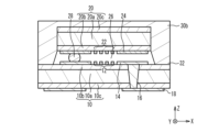
図1は、実施例1に係る弾性波デバイスの断面図である。基板10と20の積層方向をZ方向、弾性波素子12の弾性波の伝搬方向をX方向、X方向に直交する方向をY方向とする。
FIG. 1 is a cross-sectional view of an acoustic wave device according to Example 1. The stacking direction of the
図1に示すように、基板10は支持基板10aと圧電基板10bとを有する。支持基板10aは、例えばサファイア基板、アルミナ基板、スピネル基板、石英基板、水晶基板またはシリコン基板である。圧電基板10bは、例えばタンタル酸リチウム基板またはニオブ酸リチウム基板である。圧電基板10bは支持基板10aの上面に接合されている。支持基板10aの線膨張係数α2は圧電基板10bの線膨張係数α1より小さい。支持基板10aおよび圧電基板10bの厚さはそれぞれT2およびT1である。圧電基板10bと支持基板10aとは直接的に接合されていてもよいし、酸化シリコンまたは窒化アルミニウム等の絶縁体層を介し間接的に接合されていてもよい。
As shown in FIG. 1, the
基板10の上面に弾性波素子12、配線14および環状金属層32が設けられている。環状金属層32は平面視において弾性波素子12および配線14を囲むように設けられている。基板10の下面に端子18が設けられている。端子18は、弾性波素子12および22を外部と接続するためのフットパッドである。基板10を貫通するビア配線16が設けられている。ビア配線16は端子18と配線14とを電気的に接続する。配線14、ビア配線16および端子18は、例えば銅層、アルミニウム層、白金層または金層等の金属層である。環状金属層32は例えばニッケル層である。
An
基板10上に基板20が搭載されている。基板20は、基板20aと基板20bとを有する。基板20aは、例えばサファイア基板、アルミナ基板、スピネル基板、石英基板、水晶基板またはシリコン基板である。基板20bは、例えばタンタル酸リチウム基板またはニオブ酸リチウム基板である。基板20bは基板20aの上面に接合されている。基板20bの線膨張係数α4は基板20aの線膨張係数α3より大きい。基板20aおよび基板20bの厚さはそれぞれT3およびT4である。
A
基板20の下面に弾性波素子22および配線24が設けられている。配線24は例えば銅層、アルミニウム層、白金層または金層等の金属層である。基板20はバンプ28を介し基板10にフリップチップ実装(フェースダウン実装)されている。バンプ28は、例えば金バンプ、半田バンプまたは銅バンプである。バンプ28は、配線14および24と接合する。
An
基板10上に基板20を囲むように封止部30が設けられている。封止部30は、例えば半田(錫銀、錫または錫銀銅)等の金属層または樹脂等の絶縁層である。封止部30は、環状金属層32に接合されている。基板20の上面および封止部30の上面に平板状のリッド36が設けられている。リッド36は例えばコバール板等の金属板または絶縁板である。リッド36および封止部30を覆うように保護膜38が設けられている。保護膜38はニッケル膜等の金属膜または絶縁膜である。
A sealing
弾性波素子12は空隙26を介し基板20に対向している。弾性波素子22は空隙26を介し圧電基板10bに対向している。弾性波素子12および22は、封止部30、基板10、基板20およびリッド36により封止される。バンプ28は空隙26に囲まれている。端子18はビア配線16および配線14を介し弾性波素子12と電気的に接続され、さらに、バンプ28および配線24を介し弾性波素子22に電気的に接続されている。
The
支持基板10aおよび基板20aの厚さT2およびT3は例えば50μmから300μmである。圧電基板10bおよび基板20bの厚さT1およびT4は例えば0.5μmから30μmであり、例えば弾性波の波長以下である。バンプ28の厚さは例えば10μmから20μmであり、径は例えば10μmから200μmである。バンプ28が接合する配線14および24の厚さは例えば0.1μmから5μmである。
The thicknesses T2 and T3 of the
図2(a)は、実施例1における弾性波素子12の平面図、図2(b)は弾性波素子22の断面図である。図2(a)に示すように、弾性波素子12は弾性表面波共振器である。基板10の圧電基板10b上にIDT(Interdigital Transducer)40と反射器42が形成されている。IDT40は、互いに対向する1対の櫛型電極40aを有する。櫛型電極40aは、複数の電極指40bと複数の電極指40bを接続するバスバー40cとを有する。反射器42は、IDT40の両側に設けられている。
2(a) is a plan view of the
IDT40が圧電基板10bに弾性表面波を励振する。弾性波の波長は一対の櫛型電極40aの一方の櫛型電極40aの電極指40bのピッチにほぼ等しい。すなわち、弾性波の波長は一対の櫛型電極40aの電極指40bのピッチの2倍にほぼ等しい。IDT40および反射器42は例えばアルミニウム膜、銅膜またはモリブデン膜により形成される。圧電基板10b上にIDT40および反射器42を覆うように保護膜または温度補償膜が設けられていてもよい。電極指40bの配列方向が弾性波の伝搬方向であるX方向となる。電極指40bの延伸方向がY方向となる。
The
図2(b)に示すように、弾性波素子22は圧電薄膜共振器である。基板20上に圧電膜46が設けられている。圧電膜46を挟むように下部電極44および上部電極48が設けられている。下部電極44と基板20との間に空隙45が形成されている。圧電膜46の少なくとも一部を挟み下部電極44と上部電極48とが対向する領域が共振領域47である。共振領域47において、下部電極44および上部電極48は圧電膜46内に、厚み縦振動モードの弾性波を励振する。基板20は、例えばサファイア基板、スピネル基板、アルミナ基板、ガラス基板、水晶基板またはシリコン基板である。下部電極44および上部電極48は例えばルテニウム膜等の金属膜である。圧電膜46は例えば窒化アルミニウム膜である。空隙45の代わりに弾性波を反射する音響反射膜が設けられていてもよい。
As shown in FIG. 2(b), the
弾性波素子12および22は、弾性波を励振する電極を含む。このため、弾性波を制限しないように、弾性波素子12および22は空隙26に覆われている。
[実施例1の製造方法]
図3(a)から図5(b)は、実施例1に係る弾性波デバイスの製造方法を示す断面図である。図3(a)に示すように、基板20b上に基板20aを例えば表面活性化法を用い常温接合する。基板20bがタンタル酸リチウム基板またはニオブ酸リチウム基板の場合、結晶内の分極方向を揃える分極処理は行わなくてもよい。
[Production method of Example 1]
FIGS. 3(a) to 5(b) are cross-sectional views showing a method of manufacturing an acoustic wave device according to Example 1. FIG. As shown in FIG. 3A, a
図3(b)に示すように、基板20a上に弾性波素子22および配線24を形成する。図3(c)に示すように、配線24上にバンプ28を形成する。基板20bを例えばCMP(Chemical Mechanical Polishing)法を用い所望の厚さにする。
As shown in FIG. 3(b), an
図4(a)に示すように、支持基板10a上に圧電基板10bを例えば表面活性化法を用い常温接合する。圧電基板10bがタンタル酸リチウム基板またはニオブ酸リチウム基板の場合、分極処理は行われている。圧電基板10bを例えばCMP法を用い所望の厚さにする。圧電基板10bおよび支持基板10aにビア配線16を形成する。ビア配線16は支持基板10aを貫通していなくてもよい。
As shown in FIG. 4A, a
図4(b)に示すように、圧電基板10b上に弾性波素子12および配線14を形成する。図4(c)に示すように、支持基板10aを例えばCMP法を用い所望の厚さにする。これにより、ビア配線16が支持基板10aの下面に露出する。支持基板10aの下面に端子18を形成する。
As shown in FIG. 4(b), an
図5(a)に示すように、基板10上にバンプ28を介し基板20をフリップチップ実装する。基板10および20を例えば50℃から250℃に加熱し、基板20に超音波を印加しつつ、基板10と20とを互いに近づく方向に押圧する。これにより、バンプ28と配線14とが接合する。弾性波素子12と22とは空隙26を挟み対向する。
As shown in FIG. 5A, the
図5(b)に示すように、基板20を囲むように、封止部30を形成する。封止部30は環状金属層32と接合する。封止部30および基板20上にリッド36を設ける。リッド36は設けられてなくてもよい。封止部30の形成は、封止部30が半田または樹脂のとき、200℃から300℃に加熱する。その後、基板10を切断する。これにより、弾性波デバイスが個片化される。封止部30およびリッド36を囲む保護膜38を形成する。これにより、図1の弾性波デバイスが製造される。
As shown in FIG. 5(b), a sealing
[比較例1]
図6は、比較例1に係る弾性波デバイスの断面図である。図6に示すように、比較例1の弾性波デバイスでは、基板20に基板20bは設けられていない。その他の構成は実施例1と同じである。
[Comparative example 1]
FIG. 6 is a cross-sectional view of an acoustic wave device according to Comparative Example 1. As shown in FIG. 6, in the acoustic wave device of Comparative Example 1, the
支持基板10aおよび圧電基板10bとしてサファイア基板およびタンタル酸リチウム基板を用い、基板20としてシリコン基板を用いる。このとき、サファイア基板の線膨張係数は7ppm/℃であり、タンタル酸リチウム基板のX軸方位の線膨張係数は16ppm/℃である。シリコン基板の線膨張係数は2ppm/℃である。
A sapphire substrate and a lithium tantalate substrate are used as the
図5(a)のバンプ28の接合工程および図5(b)の封止部30の形成工程において高温となると、基板10は破線60のように中央が周辺に比べ基板20の方に反る。一方、基板20は破線62のようにほとんど反らない。このとき、バンプ28には垂直方向(Z方向)に熱応力が加わる。その後常温に戻ると基板10の反りは小さくなり、バンプ28には垂直方向に高温のときと逆方向の熱応力が加わる。これにより、バンプ28の剥がれ等が生じる可能性がある。
When the temperature rises in the step of bonding the
実施例1によれば、支持基板10a(第2基板)は、圧電基板10b(第1基板)の下面(第1面の反対の面)に直接的または間接的に接合されている。基板20a(第3基板)は、圧電基板10bの上面(第1面)上に設けられ、圧電基板10bの上面と空隙26を挟み対向する下面(第2面)を有する。基板20b(第4基板)は、基板20aの上面(第2面と反対の面)に直接的または間接的に接合されている。弾性波素子12および22は、圧電基板10bの上面と基板20aの下面との少なくとも一方に設けられている。バンプ28(接続層)は圧電基板10bの上面と基板20aの下面とを接続する。
According to Example 1, the
このとき、圧電基板10bの線膨張係数α1と支持基板10aの線膨張係数α2とは異なり、基板20aの線膨張係数α3は圧電基板10bの線膨張係数α1より支持基板10aの線膨張係数α2に近く、基板20bの線膨張係数α4は基板20aの線膨張係数α3より圧電基板10bの線膨張係数α1に近い。すなわち、|α3-α1|>|α3-α2|かつ|α4-α2|>|α4-α1|である。
At this time, unlike the linear expansion coefficient α1 of the
これにより、図1の破線60および62のように、基板10の反りと基板20の反りの差は、比較例1の基板10の反りと基板20の反りの差より小さくなる。よって、バンプ28に加わる応力が小さくなり、バンプ28が剥がれ等の劣化を抑制できる。|α3-α1|/2>|α3-α2|が好ましく、|α3-α1|/5>|α3-α2|がより好ましく、α3とα1は略等しいことがさらに好ましい。|α4-α2|/2>|α4-α1|が好ましく、|α4-α2|/5>|α4-α1|がより好ましく、α4とα2は略等しいことがさらに好ましい
As a result, as shown by
第1基板が圧電基板10bであり、弾性波素子12が弾性表面波素子であるとき、支持基板10aのX方向における線膨張係数α2はX方向における圧電基板10bの線膨張係数より小さくする。これにより、弾性波素子12の周波数温度係数が小さくなる。しかし、比較例1のように、バンプ28に応力が加わる。そこで、基板20aのX方向における線膨張係数をX方向における基板20bの線膨張係数より小さくする。これにより、基板10の反りと基板20の反りとの差が小さくなり、バンプ28に加わる応力を抑制できる。
When the first substrate is the
圧電基板10bは支持基板10aより薄く、基板20bは基板20aより薄い。これにより、基板10の反りと基板20の反りとの差が小さくなり、バンプ28に加わる応力を抑制できる。圧電基板10bの厚さT1は支持基板10aの厚さT2の1/2以下が好ましく、1/5以下がより好ましく、1/10以下がさらに好ましい。T1が小さすぎると基板10が反るという課題がない。よって、T1はT2の1/100以上が好ましく、1/20以上がより好ましい。T4はT3の1/2以下が好ましく,1/5以下がより好ましく、1/10以下がさらに好ましい。T4はT3の1/100以上が好ましく、1/20以上がより好ましい。
T1/T2=R1、T4/T3=R2とすると、|R1-R2|/|R1+R|は1以下が好ましく、0.5以下がより好ましく0.1以下がさらに好ましい。 When T1/T2=R1 and T4/T3=R2, |R1−R2|/|R1+R| is preferably 1 or less, more preferably 0.5 or less, and even more preferably 0.1 or less.
圧電基板10bと基板20bとは同じ材料を主成分とし、支持基板10aと基板20aとは同じ材料を主成分とすることが好ましい。これにより、α1とα4を略等しくし、α2とα3を略等しくできる。なお、基板の主成分とは、基板に主成分以外に意図的または意図せず含まれる不純物が含まれることを許容し、例えば主成分に含まれる1または複数の元素の濃度の合計が50原子%以上である。
It is preferable that the
弾性波素子22が圧電薄膜共振器のとき、基板20aは絶縁基板または半導体基板から適宜選択できる。このため基板20aの線膨張係数を基板20bの線膨張係数より支持基板10aの線膨張係数に近づくように基板20aの材料を適宜選択できる。
When the
[実施例1の変形例1]
図7は実施例1の変形例1に係る弾性波デバイスの断面図である。図7に示すように、基板20上に基板10が搭載されている。基板20は基板20b上に基板20aが接合されている。基板20a上に弾性波素子22、配線24および環状金属層32が設けられている。基板20を貫通するビア配線16が設けられている。基板20の下面に端子18が設けられている。圧電基板10b上に支持基板10aが接合されている。圧電基板10bの下面に弾性波素子12および配線14が設けられている。バンプ28は配線14および24に接合する。基板10を囲むように封止部30が設けられている。その他の構成は実施例1と同じであり説明を省略する。
[
FIG. 7 is a cross-sectional view of an acoustic wave device according to
実施例1の変形例1のように、基板20上に基板10が搭載されていてもよい。破線60および62のように、基板10の反りと基板20の反りの差は、比較例1の基板10の反りと基板20の反りの差より小さくなる。よって、バンプ28に加わる応力を抑制できる。
The
[実施例1の変形例2]
図8(a)は,実施例1の変形例2に係る弾性波デバイスの断面図、図8(b)は、平面図である。図8(b)では、封止部30aを図示している。図8(a)および図8(b)に示すように、基板10と20の平面形状はほぼ同じである。基板10と20の周縁の基板10と20との間に封止部30aが設けられている。封止部30aは、例えば銅層等の金属層であり、弾性波素子12および22を空隙26に封止する。バンプ28と封止部30aが接続層として機能する。その他の構成は実施例1と同じであり、説明を省略する。実施例1の変形例2のように、バンプ28に加えまたは代わりに封止部30aが接続層として機能してもよい。実施例1の変形例2では、熱応力による封止部30aの剥がれ等の劣化を抑制できる。
[Modification 2 of Example 1]
FIG. 8(a) is a sectional view of an acoustic wave device according to a second modification of the first embodiment, and FIG. 8(b) is a plan view. In FIG. 8(b), the sealing
図9は、実施例2に係る弾性波デバイスの断面図である。図9に示すように、基板10では、圧電基板10c上に支持基板10aが接合され、支持基板10a上に圧電基板10bが接合されている。圧電基板10bの上面に弾性波素子12および配線14が設けられている。圧電基板10cの下面には端子18が設けられている。基板10を貫通するビア配線16は配線14と端子18とを電気的に接続する。
FIG. 9 is a cross-sectional view of an acoustic wave device according to Example 2. As shown in FIG. 9, in the
基板20は、圧電基板20b上に支持基板20aが接合され、支持基板20a上に圧電基板20cが接合されている。圧電基板20bの下面に弾性波素子22および配線24が設けられている。配線14と24とはバンプ28により電気的に接続されている。基板20を囲むように封止部30bが設けられている。封止部30bが弾性波素子12および22を空隙26に封止する。封止部30bは例えばエポキシ樹脂等の樹脂である。封止部30bは金属でもよい。その他の構成は実施例1およびその変形例と同じであり説明を省略する。
In the
実施例2によれば、弾性波素子12(第1弾性波素子)は、圧電基板10b(第1圧電基板)の上面(第1面)に設けられ、複数の電極指40b(第1電極指)を有する一対の櫛型電極40aを備える。支持基板10a(第1基板)は圧電基板10bの下面(第1面とは反対の面)に直接的または間接的に接合され、電極指40bが配列される方向(第1方向)における線膨張係数が第1方向における圧電基板10bの線膨張係数より小さい。圧電基板10c(第2基板)は、支持基板10aの圧電基板10b側とは反対の面に直接的または間接的に接合され、第1方向における線膨張係数が第1方向における支持基板10aの線膨張係数より大きい。
According to the second embodiment, the acoustic wave element 12 (first acoustic wave element) is provided on the upper surface (first surface) of the
圧電基板20b(第2圧電基板)は、圧電基板10bの上面に搭載され、圧電基板20bの下面(第2面)は圧電基板10bの上面と空隙26を挟み対向する。弾性波素子22(第2弾性波素子)は、圧電基板20bの下面に設けられ、複数の電極指40b(第2電極指)を有する一対の櫛型電極40aを備える。支持基板20aは圧電基板20bの下面とは反対の面に直接的または間接的に接合され、電極指40bが配列される第2方向における線膨張係数が第2方向における圧電基板20bの線膨張係数より小さい。圧電基板20cは、支持基板20aの圧電基板20b側とは反対の面に直接的または間接的に接合され、第2方向における線膨張係数が第2方向における支持基板20aの線膨張係数より大きい。
The
これにより、支持基板10aと圧電基板10bとの線膨張係数の差に起因した基板10の反りを圧電基板10cが補償する。支持基板20aと圧電基板20bとの線膨張係数の差に起因した基板20の反りを圧電基板20cが補償する。よって、バンプ28(接続層)に加わる応力を抑制できる。
Thereby, the
圧電基板10bと10cとの線膨張係数の差は、支持基板10aと圧電基板10bとの線膨張係数の差より小さいことが好ましい。圧電基板12bと12cとの線膨張係数の差は、支持基板12aと圧電基板12bとの線膨張係数の差より小さいことが好ましい。これにより、バンプ28に加わる応力を抑制できる。
It is preferable that the difference in linear expansion coefficients between the
支持基板20aと圧電基板10bとの線膨張係数の差、および支持基板20aと圧電基板10cとの線膨張係数の差はいずれも、支持基板20aと10aとの線膨張係数の差より小さいことが好ましい。圧電基板20bと10bとの線膨張係数の差、圧電基板20bと10cとの線膨張係数の差、圧電基板20cと10bとの線膨張係数の差、および圧電基板20cと10cとの線膨張係数の差は、いずれも、圧電基板20bと支持基板10aとの線膨張係数の差、および圧電基板20cと支持基板10aとの線膨張係数の差のいずれよりも小さいことが好ましい。これにより、バンプ28に加わる応力を抑制できる。
The difference in linear expansion coefficient between the
圧電基板10bと10cは互いに同じ材料を主成分とすることが好ましく、圧電基板20bと20cは互いに同じ材料を主成分とすることが好ましい。圧電基板10bの厚さと圧電基板10cの厚さとは略等しいことが好ましい。圧電基板20bの厚さと圧電基板20cの厚さとは略等しいことが好ましい。圧電基板10bおよび10cの厚さと圧電基板20bおよび20cの厚さとは略等しいことが好ましい。支持基板10aと20aとは互いに同じ材料を主成分とすることが好ましい。支持基板10aの厚さと支持基板20aの厚さとは互いに略等しいことが好ましい。これらにより、バンプ28に加わる応力を抑制できる。
The
圧電基板10bの厚さおよび圧電基板10cの厚さは各々支持基板10aより薄いことが好ましい。圧電基板20bの厚さおよび圧電基板20cの厚さは各々支持基板20aより薄いことが好ましい。これにより、基板10の反りと基板20の反りとの差が小さくなり、バンプ28に加わる応力を抑制できる。圧電基板10bおよび10cの厚さは各々支持基板10aの厚さの1/2以下が好ましく、1/5以下がより好ましく、1/10以下がさらに好ましい。圧電基板10bが薄すぎると基板10は反らない。よって、圧電基板10bおよび10cの厚さは各々支持基板10aの厚さの1/100以上が好ましく、1/20以上がより好ましい。同様に、圧電基板20bおよび20cの厚さは各々支持基板20aの厚さの1/2以下が好ましく、1/5以下がより好ましく、1/10以下がさらに好ましい。圧電基板20bおよび20cの厚さは各々支持基板20aの厚さの1/100以上が好ましく、1/20以上がより好ましい。
It is preferable that the thickness of the
弾性波素子12の電極指40bの配列方向と弾性波素子22の電極指40bの配列方向は略平行であることが好ましい。これにより、基板10の反りと基板20との反りとの差を小さくできる。よって、バンプ28に加わる応力を小さくできる。弾性波素子12の電極指40bの配列方向と弾性波素子22の電極指40bの配列方向とのなす角度は45°以下が好ましく、30°以下がより好ましい。
It is preferable that the arrangement direction of the
実施例1の変形例2のように基板10と20とは封止部30aにより接続されていてもよい。
As in the second modification of the first embodiment, the
実施例1、2およびその変形例では、弾性波素子22として圧電薄膜共振器の例を説明したが、弾性波素子22は弾性表面波共振器でもよい。基板20の下面に設けられる機能素子として弾性波素子22の例を説明したが、機能素子は、インダクタまたはキャパシタ等の受動素子、トランジスタを含む能動素子、またはMEMS(Micro Electro Mechanical Systems)素子でもよい。
In the first and second embodiments and their modifications, the piezoelectric thin film resonator is used as the
実施例3は、フィルタおよびデュプレクサの例である。図10(a)は、実施例2に係るフィルタの回路図である。図10(a)に示すように、入力端子T1と出力端子T2との間に、1または複数の直列共振器S1からS4が直列に接続されている。入力端子T1と出力端子T2との間に、1または複数の並列共振器P1からP4が並列に接続されている。実施例2のフィルタを弾性波素子12および/または22で形成してもよい。直列共振器および並列共振器の個数等は適宜設定できる。フィルタとしてラダー型フィルタを例に説明したが、フィルタは多重モード型フィルタでもよい。
Example 3 is an example of a filter and a duplexer. FIG. 10(a) is a circuit diagram of a filter according to the second embodiment. As shown in FIG. 10(a), one or more series resonators S1 to S4 are connected in series between the input terminal T1 and the output terminal T2. One or more parallel resonators P1 to P4 are connected in parallel between the input terminal T1 and the output terminal T2. The filter of the second embodiment may be formed of the
図10(b)は、実施例2の変形例1に係るデュプレクサの回路図である。図10(b)に示すように、共通端子Antと送信端子Txとの間に送信フィルタ50が接続されている。共通端子Antと受信端子Rxとの間に受信フィルタ52が接続されている。送信フィルタ50は、送信端子Txから入力された高周波信号のうち送信帯域の信号を送信信号として共通端子Antに通過させ、他の周波数の信号を抑圧する。受信フィルタ52は、共通端子Antから入力された高周波信号のうち受信帯域の信号を受信信号として受信端子Rxに通過させ、他の周波数の信号を抑圧する。送信フィルタ50および受信フィルタ52の少なくとも一方を実施例2のフィルタとすることができる。また、送信フィルタ50を弾性波素子12で形成し、受信フィルタ52を弾性波素子22で形成してもよい。
FIG. 10(b) is a circuit diagram of a duplexer according to a first modification of the second embodiment. As shown in FIG. 10(b), a
マルチプレクサとしてデュプレクサを例に説明したがトリプレクサまたはクワッドプレクサでもよい。 Although a duplexer has been described as an example of a multiplexer, a triplexer or a quadplexer may also be used.
以上、本発明の実施例について詳述したが、本発明はかかる特定の実施例に限定されるものではなく、特許請求の範囲に記載された本発明の要旨の範囲内において、種々の変形・変更が可能である。 Although the embodiments of the present invention have been described in detail above, the present invention is not limited to these specific embodiments, and various modifications and variations can be made within the scope of the gist of the present invention as described in the claims. Changes are possible.
10a 支持基板
10b 圧電基板
12、22 弾性波素子
14、24 配線
16a、16b ビア配線
17a-17c 金属層
18 端子
20 基板
26 空隙
28a、28c バンプ
30 封止部
32 環状金属層
36 リッド
50 送信フィルタ
52 受信フィルタ
Claims (12)
前記第1基板の前記第1面とは反対の面に直接的または間接的に接合され、前記第1基板の線膨張係数より小さい線膨張係数を有し、前記第1基板より厚い第2基板と、
前記第1面上に設けられ、前記第1面と空隙を挟み対向する第2面を有し、前記第1基板の線膨張係数より前記第2基板の線膨張係数に近い線膨張係数を有する第3基板と、
前記第3基板の前記第2面とは反対の面に直接的または間接的に接合され、前記第3基板の線膨張係数より大きくかつ前記第3基板の線膨張係数より前記第1基板の線膨張係数に近い線膨張係数を有し、前記第3基板より薄い第4基板と、
前記第1面と前記第2面の少なくとも一方に設けられた弾性波素子と、
前記第1面と前記第2面とを接続する接続層と、
を備える弾性波デバイス。 a first substrate having a first surface;
a second substrate that is directly or indirectly bonded to a surface opposite to the first surface of the first substrate, has a linear expansion coefficient smaller than that of the first substrate , and is thicker than the first substrate; and,
A second surface is provided on the first surface and faces the first surface with a gap in between, and has a linear expansion coefficient closer to that of the second substrate than that of the first substrate. a third substrate;
It is directly or indirectly bonded to the surface of the third substrate opposite to the second surface, and has a linear expansion coefficient greater than that of the third substrate and less than that of the first substrate. a fourth substrate having a linear expansion coefficient close to the expansion coefficient and being thinner than the third substrate ;
an acoustic wave element provided on at least one of the first surface and the second surface;
a connection layer connecting the first surface and the second surface;
An elastic wave device equipped with
前記弾性波素子は前記第1面に設けられ、
前記弾性波素子は複数の電極指を有する一対の櫛型電極を備え、
前記第2基板の前記複数の電極指が配列される方向における線膨張係数は前記方向における前記第1基板の線膨張係数より小さく、
前記方向における前記第3基板の線膨張係数は前記方向における前記第4基板の前記方向の線膨張係数より小さい請求項1から3のいずれか一項に記載の弾性波デバイス。 The first substrate and the fourth substrate are piezoelectric substrates,
the acoustic wave element is provided on the first surface,
The acoustic wave element includes a pair of comb-shaped electrodes having a plurality of electrode fingers,
The linear expansion coefficient of the second substrate in the direction in which the plurality of electrode fingers are arranged is smaller than the linear expansion coefficient of the first substrate in the direction,
The acoustic wave device according to any one of claims 1 to 3, wherein the linear expansion coefficient of the third substrate in the direction is smaller than the linear expansion coefficient of the fourth substrate in the direction.
前記第1基板の前記第1面とは反対の面に直接的または間接的に接合され、前記第1基板の線膨張係数と異なる線膨張係数を有する第2基板と、
前記第1面上に設けられ、前記第1面と空隙を挟み対向する第2面を有し、前記第1基板の線膨張係数より前記第2基板の線膨張係数に近い線膨張係数を有する第3基板と、
前記第3基板の前記第2面とは反対の面に直接的または間接的に接合され、前記第3基板の線膨張係数より前記第1基板の線膨張係数に近い線膨張係数を有する第4基板と、
前記第1面と前記第2面の少なくとも一方に設けられた弾性波素子と、
前記第1面と前記第2面とを接続し、前記空隙を封止する封止部である接続層と、
を備える弾性波デバイス。 a first substrate having a first surface;
a second substrate that is directly or indirectly joined to a surface opposite to the first surface of the first substrate and has a linear expansion coefficient different from that of the first substrate;
A second surface is provided on the first surface and faces the first surface with a gap in between, and has a linear expansion coefficient closer to that of the second substrate than that of the first substrate. a third substrate;
A fourth substrate that is directly or indirectly bonded to a surface opposite to the second surface of the third substrate and has a linear expansion coefficient closer to that of the first substrate than that of the third substrate. A substrate and
an acoustic wave element provided on at least one of the first surface and the second surface;
a connection layer that is a sealing part that connects the first surface and the second surface and seals the gap;
An elastic wave device equipped with
前記弾性波素子は前記第1面に設けられ、
前記弾性波素子は複数の電極指を有する一対の櫛型電極を備え、
前記第2基板の前記複数の電極指が配列される方向における線膨張係数は前記方向における前記第1基板の線膨張係数より小さく、
前記方向における前記第3基板の線膨張係数は前記方向における前記第4基板の前記方向の線膨張係数より小さい請求項5に記載の弾性波デバイス。 The first substrate and the fourth substrate are piezoelectric substrates,
the acoustic wave element is provided on the first surface,
The acoustic wave element includes a pair of comb-shaped electrodes having a plurality of electrode fingers,
The linear expansion coefficient of the second substrate in the direction in which the plurality of electrode fingers are arranged is smaller than the linear expansion coefficient of the first substrate in the direction,
The acoustic wave device according to claim 5 , wherein the linear expansion coefficient of the third substrate in the direction is smaller than the linear expansion coefficient of the fourth substrate in the direction.
前記第4基板は前記第3基板より薄い請求項6に記載の弾性波デバイス。 the first substrate is thinner than the second substrate;
The acoustic wave device according to claim 6 , wherein the fourth substrate is thinner than the third substrate.
前記第2基板と前記第3基板とは同じ材料を主成分とする請求項1から9のいずれか一項に記載の弾性波デバイス。 The first substrate and the fourth substrate have the same material as a main component,
The acoustic wave device according to any one of claims 1 to 9 , wherein the second substrate and the third substrate are made of the same material as a main component.
Priority Applications (1)
| Application Number | Priority Date | Filing Date | Title |
|---|---|---|---|
| JP2019088631A JP7373301B2 (en) | 2019-05-08 | 2019-05-08 | Acoustic wave devices, filters and multiplexers |
Applications Claiming Priority (1)
| Application Number | Priority Date | Filing Date | Title |
|---|---|---|---|
| JP2019088631A JP7373301B2 (en) | 2019-05-08 | 2019-05-08 | Acoustic wave devices, filters and multiplexers |
Publications (2)
| Publication Number | Publication Date |
|---|---|
| JP2020184703A JP2020184703A (en) | 2020-11-12 |
| JP7373301B2 true JP7373301B2 (en) | 2023-11-02 |
Family
ID=73044224
Family Applications (1)
| Application Number | Title | Priority Date | Filing Date |
|---|---|---|---|
| JP2019088631A Active JP7373301B2 (en) | 2019-05-08 | 2019-05-08 | Acoustic wave devices, filters and multiplexers |
Country Status (1)
| Country | Link |
|---|---|
| JP (1) | JP7373301B2 (en) |
Families Citing this family (1)
| Publication number | Priority date | Publication date | Assignee | Title |
|---|---|---|---|---|
| WO2023171108A1 (en) * | 2022-03-09 | 2023-09-14 | MicroInnovators Laboratory株式会社 | Film structure and electronic device |
Citations (3)
| Publication number | Priority date | Publication date | Assignee | Title |
|---|---|---|---|---|
| JP2007060465A (en) | 2005-08-26 | 2007-03-08 | Seiko Epson Corp | Thin film surface acoustic wave device |
| JP2017169139A (en) | 2016-03-17 | 2017-09-21 | 太陽誘電株式会社 | Acoustic wave device |
| JP2018125773A (en) | 2017-02-02 | 2018-08-09 | 太陽誘電株式会社 | Acoustic wave device |
Family Cites Families (1)
| Publication number | Priority date | Publication date | Assignee | Title |
|---|---|---|---|---|
| JPH06216194A (en) * | 1993-01-12 | 1994-08-05 | Sony Corp | Structure for mounting semiconductor chip |
-
2019
- 2019-05-08 JP JP2019088631A patent/JP7373301B2/en active Active
Patent Citations (3)
| Publication number | Priority date | Publication date | Assignee | Title |
|---|---|---|---|---|
| JP2007060465A (en) | 2005-08-26 | 2007-03-08 | Seiko Epson Corp | Thin film surface acoustic wave device |
| JP2017169139A (en) | 2016-03-17 | 2017-09-21 | 太陽誘電株式会社 | Acoustic wave device |
| JP2018125773A (en) | 2017-02-02 | 2018-08-09 | 太陽誘電株式会社 | Acoustic wave device |
Also Published As
| Publication number | Publication date |
|---|---|
| JP2020184703A (en) | 2020-11-12 |
Similar Documents
| Publication | Publication Date | Title |
|---|---|---|
| JP6509147B2 (en) | Electronic device | |
| US10090825B2 (en) | Acoustic wave device | |
| US10250219B2 (en) | Acoustic wave device | |
| JP7370146B2 (en) | Acoustic wave devices, filters and multiplexers | |
| KR20180059353A (en) | Electronic component and method of fabricating the same | |
| JP6433930B2 (en) | Elastic wave device | |
| JP7373301B2 (en) | Acoustic wave devices, filters and multiplexers | |
| JP7426196B2 (en) | Acoustic wave devices and their manufacturing methods, filters and multiplexers | |
| JP7347955B2 (en) | Acoustic wave devices and their manufacturing methods, filters and multiplexers | |
| JP6744771B2 (en) | Electronic device and manufacturing method thereof | |
| JP7340344B2 (en) | Acoustic wave devices, filters and multiplexers | |
| JP2020191597A (en) | Elastic wave device and manufacturing method thereof | |
| JP6963448B2 (en) | Electronic components | |
| JP7340348B2 (en) | Acoustic wave devices, filters and multiplexers | |
| US20210288001A1 (en) | Electronic component, multiplexer, and module | |
| JP2023004705A (en) | Elastic wave device, filter and multiplexer | |
| JP7406341B2 (en) | Electronic components, filters and multiplexers | |
| JP7406331B2 (en) | Electronic devices, modules and wafers | |
| JP2019036784A (en) | Electronic component and method of manufacturing the same | |
| JP6653647B2 (en) | Elastic wave device | |
| JP2022118669A (en) | Acoustic wave device | |
| JP2022167077A (en) | Electronic component | |
| JP2022137801A (en) | Electronic component, filter and multiplexer | |
| JP2021034746A (en) | Electronic device and method of manufacturing the same, filter, and multiplexer | |
| JP2020184652A (en) | Electronic device, filter, and multiplexer |
Legal Events
| Date | Code | Title | Description |
|---|---|---|---|
| A621 | Written request for application examination |
Free format text: JAPANESE INTERMEDIATE CODE: A621 Effective date: 20220420 |
|
| A977 | Report on retrieval |
Free format text: JAPANESE INTERMEDIATE CODE: A971007 Effective date: 20230323 |
|
| A131 | Notification of reasons for refusal |
Free format text: JAPANESE INTERMEDIATE CODE: A131 Effective date: 20230418 |
|
| A521 | Request for written amendment filed |
Free format text: JAPANESE INTERMEDIATE CODE: A523 Effective date: 20230616 |
|
| TRDD | Decision of grant or rejection written | ||
| A01 | Written decision to grant a patent or to grant a registration (utility model) |
Free format text: JAPANESE INTERMEDIATE CODE: A01 Effective date: 20230926 |
|
| A61 | First payment of annual fees (during grant procedure) |
Free format text: JAPANESE INTERMEDIATE CODE: A61 Effective date: 20231023 |
|
| R150 | Certificate of patent or registration of utility model |
Ref document number: 7373301 Country of ref document: JP Free format text: JAPANESE INTERMEDIATE CODE: R150 |