JP7304775B2 - ウェーハの加工方法 - Google Patents
ウェーハの加工方法 Download PDFInfo
- Publication number
- JP7304775B2 JP7304775B2 JP2019157343A JP2019157343A JP7304775B2 JP 7304775 B2 JP7304775 B2 JP 7304775B2 JP 2019157343 A JP2019157343 A JP 2019157343A JP 2019157343 A JP2019157343 A JP 2019157343A JP 7304775 B2 JP7304775 B2 JP 7304775B2
- Authority
- JP
- Japan
- Prior art keywords
- resin sheet
- wafer
- annular frame
- frame
- holding
- Prior art date
- Legal status (The legal status is an assumption and is not a legal conclusion. Google has not performed a legal analysis and makes no representation as to the accuracy of the status listed.)
- Active
Links
Images


Classifications
-
- H—ELECTRICITY
- H01—ELECTRIC ELEMENTS
- H01L—SEMICONDUCTOR DEVICES NOT COVERED BY CLASS H10
- H01L21/00—Processes or apparatus adapted for the manufacture or treatment of semiconductor or solid state devices or of parts thereof
- H01L21/67—Apparatus specially adapted for handling semiconductor or electric solid state devices during manufacture or treatment thereof; Apparatus specially adapted for handling wafers during manufacture or treatment of semiconductor or electric solid state devices or components ; Apparatus not specifically provided for elsewhere
- H01L21/683—Apparatus specially adapted for handling semiconductor or electric solid state devices during manufacture or treatment thereof; Apparatus specially adapted for handling wafers during manufacture or treatment of semiconductor or electric solid state devices or components ; Apparatus not specifically provided for elsewhere for supporting or gripping
- H01L21/6835—Apparatus specially adapted for handling semiconductor or electric solid state devices during manufacture or treatment thereof; Apparatus specially adapted for handling wafers during manufacture or treatment of semiconductor or electric solid state devices or components ; Apparatus not specifically provided for elsewhere for supporting or gripping using temporarily an auxiliary support
- H01L21/6836—Wafer tapes, e.g. grinding or dicing support tapes
-
- B—PERFORMING OPERATIONS; TRANSPORTING
- B81—MICROSTRUCTURAL TECHNOLOGY
- B81C—PROCESSES OR APPARATUS SPECIALLY ADAPTED FOR THE MANUFACTURE OR TREATMENT OF MICROSTRUCTURAL DEVICES OR SYSTEMS
- B81C99/00—Subject matter not provided for in other groups of this subclass
- B81C99/0075—Manufacture of substrate-free structures
- B81C99/008—Manufacture of substrate-free structures separating the processed structure from a mother substrate
-
- H—ELECTRICITY
- H01—ELECTRIC ELEMENTS
- H01L—SEMICONDUCTOR DEVICES NOT COVERED BY CLASS H10
- H01L21/00—Processes or apparatus adapted for the manufacture or treatment of semiconductor or solid state devices or of parts thereof
- H01L21/02—Manufacture or treatment of semiconductor devices or of parts thereof
- H01L21/04—Manufacture or treatment of semiconductor devices or of parts thereof the devices having at least one potential-jump barrier or surface barrier, e.g. PN junction, depletion layer or carrier concentration layer
- H01L21/18—Manufacture or treatment of semiconductor devices or of parts thereof the devices having at least one potential-jump barrier or surface barrier, e.g. PN junction, depletion layer or carrier concentration layer the devices having semiconductor bodies comprising elements of Group IV of the Periodic System or AIIIBV compounds with or without impurities, e.g. doping materials
- H01L21/26—Bombardment with radiation
- H01L21/263—Bombardment with radiation with high-energy radiation
- H01L21/268—Bombardment with radiation with high-energy radiation using electromagnetic radiation, e.g. laser radiation
-
- H—ELECTRICITY
- H01—ELECTRIC ELEMENTS
- H01L—SEMICONDUCTOR DEVICES NOT COVERED BY CLASS H10
- H01L21/00—Processes or apparatus adapted for the manufacture or treatment of semiconductor or solid state devices or of parts thereof
- H01L21/70—Manufacture or treatment of devices consisting of a plurality of solid state components formed in or on a common substrate or of parts thereof; Manufacture of integrated circuit devices or of parts thereof
- H01L21/77—Manufacture or treatment of devices consisting of a plurality of solid state components or integrated circuits formed in, or on, a common substrate
- H01L21/78—Manufacture or treatment of devices consisting of a plurality of solid state components or integrated circuits formed in, or on, a common substrate with subsequent division of the substrate into plural individual devices
-
- H—ELECTRICITY
- H01—ELECTRIC ELEMENTS
- H01L—SEMICONDUCTOR DEVICES NOT COVERED BY CLASS H10
- H01L2221/00—Processes or apparatus adapted for the manufacture or treatment of semiconductor or solid state devices or of parts thereof covered by H01L21/00
- H01L2221/67—Apparatus for handling semiconductor or electric solid state devices during manufacture or treatment thereof; Apparatus for handling wafers during manufacture or treatment of semiconductor or electric solid state devices or components; Apparatus not specifically provided for elsewhere
- H01L2221/683—Apparatus for handling semiconductor or electric solid state devices during manufacture or treatment thereof; Apparatus for handling wafers during manufacture or treatment of semiconductor or electric solid state devices or components; Apparatus not specifically provided for elsewhere for supporting or gripping
- H01L2221/68304—Apparatus for handling semiconductor or electric solid state devices during manufacture or treatment thereof; Apparatus for handling wafers during manufacture or treatment of semiconductor or electric solid state devices or components; Apparatus not specifically provided for elsewhere for supporting or gripping using temporarily an auxiliary support
- H01L2221/68327—Apparatus for handling semiconductor or electric solid state devices during manufacture or treatment thereof; Apparatus for handling wafers during manufacture or treatment of semiconductor or electric solid state devices or components; Apparatus not specifically provided for elsewhere for supporting or gripping using temporarily an auxiliary support used during dicing or grinding
- H01L2221/68336—Apparatus for handling semiconductor or electric solid state devices during manufacture or treatment thereof; Apparatus for handling wafers during manufacture or treatment of semiconductor or electric solid state devices or components; Apparatus not specifically provided for elsewhere for supporting or gripping using temporarily an auxiliary support used during dicing or grinding involving stretching of the auxiliary support post dicing
-
- H—ELECTRICITY
- H01—ELECTRIC ELEMENTS
- H01L—SEMICONDUCTOR DEVICES NOT COVERED BY CLASS H10
- H01L2221/00—Processes or apparatus adapted for the manufacture or treatment of semiconductor or solid state devices or of parts thereof covered by H01L21/00
- H01L2221/67—Apparatus for handling semiconductor or electric solid state devices during manufacture or treatment thereof; Apparatus for handling wafers during manufacture or treatment of semiconductor or electric solid state devices or components; Apparatus not specifically provided for elsewhere
- H01L2221/683—Apparatus for handling semiconductor or electric solid state devices during manufacture or treatment thereof; Apparatus for handling wafers during manufacture or treatment of semiconductor or electric solid state devices or components; Apparatus not specifically provided for elsewhere for supporting or gripping
- H01L2221/68304—Apparatus for handling semiconductor or electric solid state devices during manufacture or treatment thereof; Apparatus for handling wafers during manufacture or treatment of semiconductor or electric solid state devices or components; Apparatus not specifically provided for elsewhere for supporting or gripping using temporarily an auxiliary support
- H01L2221/6834—Apparatus for handling semiconductor or electric solid state devices during manufacture or treatment thereof; Apparatus for handling wafers during manufacture or treatment of semiconductor or electric solid state devices or components; Apparatus not specifically provided for elsewhere for supporting or gripping using temporarily an auxiliary support used to protect an active side of a device or wafer
Description
本発明の実施形態1に係るウェーハの加工方法を図面に基づいて説明する。図1は、実施形態1に係るウェーハの加工方法の加工対象のウェーハの一例を示す斜視図である。図2は、実施形態1に係るウェーハの加工方法の流れを示すフローチャートである。
図3は、図2に示されたウェーハの加工方法のフレームユニット形成ステップで形成されるフレームユニットの斜視図である。図4は、図3に示されたフレームユニットの粘着テープの要部の断面図である。フレームユニット形成ステップST1は、環状フレーム10の開口を塞ぐ粘着テープ11にウェーハ1の基板2の裏面6が貼着したフレームユニット7を形成するステップである。
図5は、図2に示されたウェーハの加工方法の樹脂シート準備ステップで準備される樹脂シートの斜視図である。樹脂シート準備ステップST2は、環状フレーム10の開口よりも直径が大きくウェーハ1の保護部材となる樹脂シートを準備するステップである。
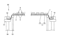
図6は、図2に示されたウェーハの加工方法の樹脂シート固定ステップで樹脂シートが固定されたフレームユニットの断面図である。樹脂シート固定ステップST3は、フレームユニット7のウェーハ1の基板2の表面3側から環状フレーム10の開口を樹脂シート17で覆い、環状フレーム10に対面する樹脂シート17の外周縁を環状フレーム10に固定するステップである。
図7は、図2に示されたウェーハの加工方法の貫通穴形成ステップで環状フレームに固定された樹脂シートに貫通穴が形成されたフレームユニットの断面図である。図8は、図7に示されたフレームユニットの平面図である。貫通穴形成ステップST4は、樹脂シート17のウェーハ1の外周の領域に貫通穴16を形成するステップである。
図9は、図2に示されたウェーハの加工方法の保持ステップを示す断面図である。保持ステップST5は、樹脂シート固定ステップST3と貫通穴形成ステップST4を実施後、図9に示すレーザー加工装置20のチャックテーブル21を用い、フレームユニット7の樹脂シート17側をチャックテーブル21の保持面22で吸引保持しつつ環状フレーム10をフレーム保持部23で保持面22よりも下方側に引き落として固定するステップである。
図10は、図2に示されたウェーハの加工方法のレーザー光線照射ステップを示す断面図である。レーザー光線照射ステップST6は、保持ステップST5実施後、粘着テープ11とウェーハ1に対して透過性を有する波長のレーザー光線33をウェーハ1の基板2の内部に集光点34を位置付けた状態で、レーザー光線33を粘着テープ11側から照射し、ウェーハ1の内部にストリート4に沿った改質層9を形成するステップである。
図11は、図2に示されたウェーハの加工方法の樹脂シート剥離ステップを示す断面図である。樹脂シート剥離ステップST7は、レーザー光線照射ステップST6を実施後、環状フレーム10から樹脂シート17を剥離するステップである。
図12は、図2に示されたウェーハの加工方法の破断ステップにおいてウェーハをエキスパンド装置に保持した状態の断面図である。図13は、図2に示されたウェーハの加工方法の破断ステップにおいて粘着テープを拡張した状態の断面図である。破断ステップST8は、樹脂シート剥離ステップST7実施後、粘着テープ11を面方向に拡張して改質層9に沿ってウェーハ1を個々のデバイスチップ8に破断するステップである。
本発明の実施形態2に係るウェーハの加工方法を図面に基づいて説明する。図14は、実施形態2に係るウェーハの加工方法の樹脂シート固定ステップで樹脂シートが固定されたフレームユニットの断面図である。図14は、実施形態1と同一部分に同一符号を付して説明を省略する。
本発明の実施形態3に係るウェーハの加工方法を図面に基づいて説明する。図15は、実施形態3に係るウェーハの加工方法の流れを示すフローチャートである。図16は、図15に示されたウェーハの加工方法の紫外線照射ステップを示す断面図である。図15及び図16は、実施形態1と同一部分に同一符号を付して説明を省略する。
3 表面
4 ストリート
5 デバイス
6 裏面
7 フレームユニット
9 改質層
10 環状フレーム(被着体)
11 粘着テープ
13 糊層
15 糊層
16 貫通穴
17 樹脂シート
21 チャックテーブル
22 保持面
23 フレーム保持部
24 テーブル本体
33 レーザー光線
34 集光点
61 紫外線
ST1 フレームユニット形成ステップ
ST2 樹脂シート準備ステップ
ST3 樹脂シート固定ステップ
ST4 貫通穴形成ステップ
ST5 保持ステップ
ST6 レーザー光線照射ステップ
ST7 樹脂シート剥離ステップ
ST8 破断ステップ
ST10 紫外線照射ステップ
Claims (6)
- 交差するストリートで区画された表面の複数の領域にデバイスが形成されたウェーハを加工するウェーハの加工方法であって、
環状フレームの開口を塞ぐ粘着テープにウェーハの裏面が貼着したフレームユニットを形成するフレームユニット形成ステップと、
環状フレームの開口より直径が大きくウェーハの保護部材となる樹脂シートを準備する樹脂シート準備ステップと、
該フレームユニットの該ウェーハの表面側から該環状フレームの開口を該樹脂シートで覆い、該環状フレームに対面する該樹脂シートの外周縁を該環状フレームに固定する樹脂シート固定ステップと、
該樹脂シートの該ウェーハの外周の領域に貫通穴を形成する貫通穴形成ステップと、
該樹脂シート固定ステップと該貫通穴形成ステップを実施後、該ウェーハの直径よりも大きい保持面を有するテーブル本体と、該テーブル本体の外周で該環状フレームを該保持面より引き落として固定するフレーム保持部とを備えるチャックテーブルを用い、該フレームユニットの該樹脂シート側を該保持面で吸引保持しつつ該環状フレームを該フレーム保持部で引き落として固定する保持ステップと、
該保持ステップ実施後、該粘着テープとウェーハに対して透過性を有する波長のレーザー光線をウェーハの内部に集光点を位置付けた状態で該粘着テープ側から照射し、ウェーハの内部に該ストリートに沿った改質層を形成するレーザー光線照射ステップと、
該レーザー光線照射ステップを実施後、該環状フレームから該樹脂シートを剥離する樹脂シート剥離ステップと、を備え、
該保持ステップでは、
ウェーハの表面が該保持面に吸引されるのを該樹脂シートで抑制しつつ、該保持面からの負圧が該樹脂シートの該貫通穴を介して該樹脂シートに対面する該粘着テープを吸引し、該フレームユニットの該チャックテーブルへの固定が保持されるウェーハの加工方法。 - 該ウェーハの該デバイスは、MEMSである請求項1に記載のウェーハの加工方法。
- 該樹脂シート剥離ステップ実施後、該粘着テープを面方向に拡張して該改質層に沿って該ウェーハを破断する破断ステップを備える請求項1または請求項2に記載のウェーハの加工方法。
- 該粘着テープは、紫外線硬化型の糊層で被着体に貼着し、
該フレームユニット形成ステップの後で該樹脂シート固定ステップの前に、該粘着テープの該環状フレームとウェーハとの間で露出した領域に紫外線を照射し該糊層の粘着力を低下させる紫外線照射ステップ備える請求項1、請求項2または請求項3に記載のウェーハの加工方法。 - 該樹脂シート固定ステップでは、該樹脂シートの該環状フレームに対応する領域に積層された糊層で該樹脂シートが該環状フレームに固定される請求項1、請求項2、請求項3または請求項4に記載のウェーハの加工方法。
- 該樹脂シート固定ステップでは、該樹脂シートの該環状フレームに対応する領域を加熱し、該樹脂シートが該環状フレームに密着して固定される請求項1、請求項2、請求項3または請求項4に記載のウェーハの加工方法。
Priority Applications (3)
| Application Number | Priority Date | Filing Date | Title |
|---|---|---|---|
| JP2019157343A JP7304775B2 (ja) | 2019-08-29 | 2019-08-29 | ウェーハの加工方法 |
| TW109129338A TWI828938B (zh) | 2019-08-29 | 2020-08-27 | 晶圓的加工方法 |
| US17/004,441 US11315821B2 (en) | 2019-08-29 | 2020-08-27 | Processing method for wafer |
Applications Claiming Priority (1)
| Application Number | Priority Date | Filing Date | Title |
|---|---|---|---|
| JP2019157343A JP7304775B2 (ja) | 2019-08-29 | 2019-08-29 | ウェーハの加工方法 |
Publications (2)
| Publication Number | Publication Date |
|---|---|
| JP2021034704A JP2021034704A (ja) | 2021-03-01 |
| JP7304775B2 true JP7304775B2 (ja) | 2023-07-07 |
Family
ID=74677730
Family Applications (1)
| Application Number | Title | Priority Date | Filing Date |
|---|---|---|---|
| JP2019157343A Active JP7304775B2 (ja) | 2019-08-29 | 2019-08-29 | ウェーハの加工方法 |
Country Status (3)
| Country | Link |
|---|---|
| US (1) | US11315821B2 (ja) |
| JP (1) | JP7304775B2 (ja) |
| TW (1) | TWI828938B (ja) |
Families Citing this family (1)
| Publication number | Priority date | Publication date | Assignee | Title |
|---|---|---|---|---|
| JP7140626B2 (ja) * | 2018-10-10 | 2022-09-21 | 株式会社ディスコ | リングフレームの保持機構 |
Citations (6)
| Publication number | Priority date | Publication date | Assignee | Title |
|---|---|---|---|---|
| JP2012109338A (ja) | 2010-11-16 | 2012-06-07 | Disco Abrasive Syst Ltd | ワークの加工方法及びダイシングテープ |
| JP2013229403A (ja) | 2012-04-24 | 2013-11-07 | Disco Abrasive Syst Ltd | 加工装置のチャックテーブル機構 |
| JP2015233051A (ja) | 2014-06-09 | 2015-12-24 | 株式会社ディスコ | ウェーハの分割方法 |
| JP2016062928A (ja) | 2014-09-12 | 2016-04-25 | 株式会社東芝 | 半導体装置の製造装置と半導体装置の製造方法 |
| JP2016115827A (ja) | 2014-12-16 | 2016-06-23 | 株式会社ディスコ | シート状部材 |
| US20190140008A1 (en) | 2017-11-07 | 2019-05-09 | Commissariat A L'energie Atomique Et Aux Energies Alternatives | Method for producing curved electronic circuits |
Family Cites Families (4)
| Publication number | Priority date | Publication date | Assignee | Title |
|---|---|---|---|---|
| US7608523B2 (en) * | 2005-08-26 | 2009-10-27 | Disco Corporation | Wafer processing method and adhesive tape used in the wafer processing method |
| JP2013229450A (ja) | 2012-04-25 | 2013-11-07 | Disco Abrasive Syst Ltd | ウエーハのレーザー加工方法 |
| JP6360411B2 (ja) * | 2014-10-09 | 2018-07-18 | 株式会社ディスコ | ウエーハの加工方法 |
| US10658240B1 (en) * | 2018-12-31 | 2020-05-19 | Texas Instruments Incorporated | Semiconductor die singulation |
-
2019
- 2019-08-29 JP JP2019157343A patent/JP7304775B2/ja active Active
-
2020
- 2020-08-27 US US17/004,441 patent/US11315821B2/en active Active
- 2020-08-27 TW TW109129338A patent/TWI828938B/zh active
Patent Citations (6)
| Publication number | Priority date | Publication date | Assignee | Title |
|---|---|---|---|---|
| JP2012109338A (ja) | 2010-11-16 | 2012-06-07 | Disco Abrasive Syst Ltd | ワークの加工方法及びダイシングテープ |
| JP2013229403A (ja) | 2012-04-24 | 2013-11-07 | Disco Abrasive Syst Ltd | 加工装置のチャックテーブル機構 |
| JP2015233051A (ja) | 2014-06-09 | 2015-12-24 | 株式会社ディスコ | ウェーハの分割方法 |
| JP2016062928A (ja) | 2014-09-12 | 2016-04-25 | 株式会社東芝 | 半導体装置の製造装置と半導体装置の製造方法 |
| JP2016115827A (ja) | 2014-12-16 | 2016-06-23 | 株式会社ディスコ | シート状部材 |
| US20190140008A1 (en) | 2017-11-07 | 2019-05-09 | Commissariat A L'energie Atomique Et Aux Energies Alternatives | Method for producing curved electronic circuits |
Also Published As
| Publication number | Publication date |
|---|---|
| TW202109645A (zh) | 2021-03-01 |
| US11315821B2 (en) | 2022-04-26 |
| JP2021034704A (ja) | 2021-03-01 |
| TWI828938B (zh) | 2024-01-11 |
| US20210066111A1 (en) | 2021-03-04 |
Similar Documents
| Publication | Publication Date | Title |
|---|---|---|
| TWI724020B (zh) | 處理晶圓的方法及用於該方法的保護片 | |
| TWI713976B (zh) | 處理晶圓的方法 | |
| TWI742343B (zh) | 處理晶圓的方法 | |
| CN109417049B (zh) | 处理背面上具有突出物的晶片的方法 | |
| TW200411755A (en) | Method of processing a semiconductor wafer | |
| JP6782617B2 (ja) | 被加工物の固定方法、及び被加工物の加工方法 | |
| CN110858564B (zh) | 加工基板的方法 | |
| JP7304775B2 (ja) | ウェーハの加工方法 | |
| JP2021082631A (ja) | 保護部材の設置方法、被加工物の加工方法及び保護部材の製造方法 | |
| JP6298699B2 (ja) | ウェーハの加工方法 | |
| TWI790454B (zh) | 加工基材之方法 | |
| TW202307947A (zh) | 加工基板的方法和用於加工基板的系統 | |
| TWI804947B (zh) | 處理基板的方法 | |
| TWI822316B (zh) | 加工基板的方法 | |
| JP2022054894A (ja) | ウェーハの加工方法 | |
| TW201503253A (zh) | 晶圓之加工方法 | |
| TW202305903A (zh) | 具保護膜之晶片的製造方法 | |
| JP2019096801A (ja) | ウェーハの加工方法 | |
| JP2021019136A (ja) | ウェーハの加工方法 |
Legal Events
| Date | Code | Title | Description |
|---|---|---|---|
| A621 | Written request for application examination |
Free format text: JAPANESE INTERMEDIATE CODE: A621 Effective date: 20220617 |
|
| A977 | Report on retrieval |
Free format text: JAPANESE INTERMEDIATE CODE: A971007 Effective date: 20230516 |
|
| TRDD | Decision of grant or rejection written | ||
| A01 | Written decision to grant a patent or to grant a registration (utility model) |
Free format text: JAPANESE INTERMEDIATE CODE: A01 Effective date: 20230613 |
|
| A61 | First payment of annual fees (during grant procedure) |
Free format text: JAPANESE INTERMEDIATE CODE: A61 Effective date: 20230627 |
|
| R150 | Certificate of patent or registration of utility model |
Ref document number: 7304775 Country of ref document: JP Free format text: JAPANESE INTERMEDIATE CODE: R150 |