US10658240B1 - Semiconductor die singulation - Google Patents
Semiconductor die singulation Download PDFInfo
- Publication number
- US10658240B1 US10658240B1 US16/291,995 US201916291995A US10658240B1 US 10658240 B1 US10658240 B1 US 10658240B1 US 201916291995 A US201916291995 A US 201916291995A US 10658240 B1 US10658240 B1 US 10658240B1
- Authority
- US
- United States
- Prior art keywords
- dicing tape
- dicing
- semiconductor
- tape
- wafer
- Prior art date
- Legal status (The legal status is an assumption and is not a legal conclusion. Google has not performed a legal analysis and makes no representation as to the accuracy of the status listed.)
- Active
Links
Images


Classifications
-
- H—ELECTRICITY
- H01—ELECTRIC ELEMENTS
- H01L—SEMICONDUCTOR DEVICES NOT COVERED BY CLASS H10
- H01L21/00—Processes or apparatus adapted for the manufacture or treatment of semiconductor or solid state devices or of parts thereof
- H01L21/70—Manufacture or treatment of devices consisting of a plurality of solid state components formed in or on a common substrate or of parts thereof; Manufacture of integrated circuit devices or of parts thereof
- H01L21/77—Manufacture or treatment of devices consisting of a plurality of solid state components or integrated circuits formed in, or on, a common substrate
- H01L21/78—Manufacture or treatment of devices consisting of a plurality of solid state components or integrated circuits formed in, or on, a common substrate with subsequent division of the substrate into plural individual devices
-
- B—PERFORMING OPERATIONS; TRANSPORTING
- B23—MACHINE TOOLS; METAL-WORKING NOT OTHERWISE PROVIDED FOR
- B23K—SOLDERING OR UNSOLDERING; WELDING; CLADDING OR PLATING BY SOLDERING OR WELDING; CUTTING BY APPLYING HEAT LOCALLY, e.g. FLAME CUTTING; WORKING BY LASER BEAM
- B23K26/00—Working by laser beam, e.g. welding, cutting or boring
- B23K26/36—Removing material
- B23K26/362—Laser etching
- B23K26/364—Laser etching for making a groove or trench, e.g. for scribing a break initiation groove
-
- H—ELECTRICITY
- H01—ELECTRIC ELEMENTS
- H01L—SEMICONDUCTOR DEVICES NOT COVERED BY CLASS H10
- H01L21/00—Processes or apparatus adapted for the manufacture or treatment of semiconductor or solid state devices or of parts thereof
- H01L21/02—Manufacture or treatment of semiconductor devices or of parts thereof
- H01L21/04—Manufacture or treatment of semiconductor devices or of parts thereof the devices having at least one potential-jump barrier or surface barrier, e.g. PN junction, depletion layer or carrier concentration layer
- H01L21/50—Assembly of semiconductor devices using processes or apparatus not provided for in a single one of the subgroups H01L21/06 - H01L21/326, e.g. sealing of a cap to a base of a container
- H01L21/56—Encapsulations, e.g. encapsulation layers, coatings
- H01L21/561—Batch processing
-
- H—ELECTRICITY
- H01—ELECTRIC ELEMENTS
- H01L—SEMICONDUCTOR DEVICES NOT COVERED BY CLASS H10
- H01L21/00—Processes or apparatus adapted for the manufacture or treatment of semiconductor or solid state devices or of parts thereof
- H01L21/02—Manufacture or treatment of semiconductor devices or of parts thereof
- H01L21/04—Manufacture or treatment of semiconductor devices or of parts thereof the devices having at least one potential-jump barrier or surface barrier, e.g. PN junction, depletion layer or carrier concentration layer
- H01L21/50—Assembly of semiconductor devices using processes or apparatus not provided for in a single one of the subgroups H01L21/06 - H01L21/326, e.g. sealing of a cap to a base of a container
- H01L21/56—Encapsulations, e.g. encapsulation layers, coatings
- H01L21/565—Moulds
-
- H—ELECTRICITY
- H01—ELECTRIC ELEMENTS
- H01L—SEMICONDUCTOR DEVICES NOT COVERED BY CLASS H10
- H01L21/00—Processes or apparatus adapted for the manufacture or treatment of semiconductor or solid state devices or of parts thereof
- H01L21/67—Apparatus specially adapted for handling semiconductor or electric solid state devices during manufacture or treatment thereof; Apparatus specially adapted for handling wafers during manufacture or treatment of semiconductor or electric solid state devices or components ; Apparatus not specifically provided for elsewhere
- H01L21/67005—Apparatus not specifically provided for elsewhere
- H01L21/67011—Apparatus for manufacture or treatment
- H01L21/67092—Apparatus for mechanical treatment
-
- H—ELECTRICITY
- H01—ELECTRIC ELEMENTS
- H01L—SEMICONDUCTOR DEVICES NOT COVERED BY CLASS H10
- H01L21/00—Processes or apparatus adapted for the manufacture or treatment of semiconductor or solid state devices or of parts thereof
- H01L21/67—Apparatus specially adapted for handling semiconductor or electric solid state devices during manufacture or treatment thereof; Apparatus specially adapted for handling wafers during manufacture or treatment of semiconductor or electric solid state devices or components ; Apparatus not specifically provided for elsewhere
- H01L21/67005—Apparatus not specifically provided for elsewhere
- H01L21/67011—Apparatus for manufacture or treatment
- H01L21/67098—Apparatus for thermal treatment
- H01L21/67115—Apparatus for thermal treatment mainly by radiation
-
- H—ELECTRICITY
- H01—ELECTRIC ELEMENTS
- H01L—SEMICONDUCTOR DEVICES NOT COVERED BY CLASS H10
- H01L21/00—Processes or apparatus adapted for the manufacture or treatment of semiconductor or solid state devices or of parts thereof
- H01L21/67—Apparatus specially adapted for handling semiconductor or electric solid state devices during manufacture or treatment thereof; Apparatus specially adapted for handling wafers during manufacture or treatment of semiconductor or electric solid state devices or components ; Apparatus not specifically provided for elsewhere
- H01L21/67005—Apparatus not specifically provided for elsewhere
- H01L21/67011—Apparatus for manufacture or treatment
- H01L21/67132—Apparatus for placing on an insulating substrate, e.g. tape
-
- H—ELECTRICITY
- H01—ELECTRIC ELEMENTS
- H01L—SEMICONDUCTOR DEVICES NOT COVERED BY CLASS H10
- H01L21/00—Processes or apparatus adapted for the manufacture or treatment of semiconductor or solid state devices or of parts thereof
- H01L21/67—Apparatus specially adapted for handling semiconductor or electric solid state devices during manufacture or treatment thereof; Apparatus specially adapted for handling wafers during manufacture or treatment of semiconductor or electric solid state devices or components ; Apparatus not specifically provided for elsewhere
- H01L21/683—Apparatus specially adapted for handling semiconductor or electric solid state devices during manufacture or treatment thereof; Apparatus specially adapted for handling wafers during manufacture or treatment of semiconductor or electric solid state devices or components ; Apparatus not specifically provided for elsewhere for supporting or gripping
- H01L21/6835—Apparatus specially adapted for handling semiconductor or electric solid state devices during manufacture or treatment thereof; Apparatus specially adapted for handling wafers during manufacture or treatment of semiconductor or electric solid state devices or components ; Apparatus not specifically provided for elsewhere for supporting or gripping using temporarily an auxiliary support
- H01L21/6836—Wafer tapes, e.g. grinding or dicing support tapes
-
- H—ELECTRICITY
- H01—ELECTRIC ELEMENTS
- H01L—SEMICONDUCTOR DEVICES NOT COVERED BY CLASS H10
- H01L24/00—Arrangements for connecting or disconnecting semiconductor or solid-state bodies; Methods or apparatus related thereto
- H01L24/01—Means for bonding being attached to, or being formed on, the surface to be connected, e.g. chip-to-package, die-attach, "first-level" interconnects; Manufacturing methods related thereto
- H01L24/02—Bonding areas ; Manufacturing methods related thereto
- H01L24/07—Structure, shape, material or disposition of the bonding areas after the connecting process
- H01L24/09—Structure, shape, material or disposition of the bonding areas after the connecting process of a plurality of bonding areas
-
- H—ELECTRICITY
- H01—ELECTRIC ELEMENTS
- H01L—SEMICONDUCTOR DEVICES NOT COVERED BY CLASS H10
- H01L24/00—Arrangements for connecting or disconnecting semiconductor or solid-state bodies; Methods or apparatus related thereto
- H01L24/01—Means for bonding being attached to, or being formed on, the surface to be connected, e.g. chip-to-package, die-attach, "first-level" interconnects; Manufacturing methods related thereto
- H01L24/42—Wire connectors; Manufacturing methods related thereto
- H01L24/47—Structure, shape, material or disposition of the wire connectors after the connecting process
- H01L24/49—Structure, shape, material or disposition of the wire connectors after the connecting process of a plurality of wire connectors
-
- H—ELECTRICITY
- H01—ELECTRIC ELEMENTS
- H01L—SEMICONDUCTOR DEVICES NOT COVERED BY CLASS H10
- H01L24/00—Arrangements for connecting or disconnecting semiconductor or solid-state bodies; Methods or apparatus related thereto
- H01L24/93—Batch processes
- H01L24/95—Batch processes at chip-level, i.e. with connecting carried out on a plurality of singulated devices, i.e. on diced chips
- H01L24/97—Batch processes at chip-level, i.e. with connecting carried out on a plurality of singulated devices, i.e. on diced chips the devices being connected to a common substrate, e.g. interposer, said common substrate being separable into individual assemblies after connecting
-
- B—PERFORMING OPERATIONS; TRANSPORTING
- B23—MACHINE TOOLS; METAL-WORKING NOT OTHERWISE PROVIDED FOR
- B23K—SOLDERING OR UNSOLDERING; WELDING; CLADDING OR PLATING BY SOLDERING OR WELDING; CUTTING BY APPLYING HEAT LOCALLY, e.g. FLAME CUTTING; WORKING BY LASER BEAM
- B23K2101/00—Articles made by soldering, welding or cutting
- B23K2101/36—Electric or electronic devices
- B23K2101/40—Semiconductor devices
-
- H—ELECTRICITY
- H01—ELECTRIC ELEMENTS
- H01L—SEMICONDUCTOR DEVICES NOT COVERED BY CLASS H10
- H01L2221/00—Processes or apparatus adapted for the manufacture or treatment of semiconductor or solid state devices or of parts thereof covered by H01L21/00
- H01L2221/67—Apparatus for handling semiconductor or electric solid state devices during manufacture or treatment thereof; Apparatus for handling wafers during manufacture or treatment of semiconductor or electric solid state devices or components; Apparatus not specifically provided for elsewhere
- H01L2221/683—Apparatus for handling semiconductor or electric solid state devices during manufacture or treatment thereof; Apparatus for handling wafers during manufacture or treatment of semiconductor or electric solid state devices or components; Apparatus not specifically provided for elsewhere for supporting or gripping
- H01L2221/68304—Apparatus for handling semiconductor or electric solid state devices during manufacture or treatment thereof; Apparatus for handling wafers during manufacture or treatment of semiconductor or electric solid state devices or components; Apparatus not specifically provided for elsewhere for supporting or gripping using temporarily an auxiliary support
- H01L2221/68327—Apparatus for handling semiconductor or electric solid state devices during manufacture or treatment thereof; Apparatus for handling wafers during manufacture or treatment of semiconductor or electric solid state devices or components; Apparatus not specifically provided for elsewhere for supporting or gripping using temporarily an auxiliary support used during dicing or grinding
-
- H—ELECTRICITY
- H01—ELECTRIC ELEMENTS
- H01L—SEMICONDUCTOR DEVICES NOT COVERED BY CLASS H10
- H01L2221/00—Processes or apparatus adapted for the manufacture or treatment of semiconductor or solid state devices or of parts thereof covered by H01L21/00
- H01L2221/67—Apparatus for handling semiconductor or electric solid state devices during manufacture or treatment thereof; Apparatus for handling wafers during manufacture or treatment of semiconductor or electric solid state devices or components; Apparatus not specifically provided for elsewhere
- H01L2221/683—Apparatus for handling semiconductor or electric solid state devices during manufacture or treatment thereof; Apparatus for handling wafers during manufacture or treatment of semiconductor or electric solid state devices or components; Apparatus not specifically provided for elsewhere for supporting or gripping
- H01L2221/68304—Apparatus for handling semiconductor or electric solid state devices during manufacture or treatment thereof; Apparatus for handling wafers during manufacture or treatment of semiconductor or electric solid state devices or components; Apparatus not specifically provided for elsewhere for supporting or gripping using temporarily an auxiliary support
- H01L2221/6834—Apparatus for handling semiconductor or electric solid state devices during manufacture or treatment thereof; Apparatus for handling wafers during manufacture or treatment of semiconductor or electric solid state devices or components; Apparatus not specifically provided for elsewhere for supporting or gripping using temporarily an auxiliary support used to protect an active side of a device or wafer
-
- H—ELECTRICITY
- H01—ELECTRIC ELEMENTS
- H01L—SEMICONDUCTOR DEVICES NOT COVERED BY CLASS H10
- H01L2221/00—Processes or apparatus adapted for the manufacture or treatment of semiconductor or solid state devices or of parts thereof covered by H01L21/00
- H01L2221/67—Apparatus for handling semiconductor or electric solid state devices during manufacture or treatment thereof; Apparatus for handling wafers during manufacture or treatment of semiconductor or electric solid state devices or components; Apparatus not specifically provided for elsewhere
- H01L2221/683—Apparatus for handling semiconductor or electric solid state devices during manufacture or treatment thereof; Apparatus for handling wafers during manufacture or treatment of semiconductor or electric solid state devices or components; Apparatus not specifically provided for elsewhere for supporting or gripping
- H01L2221/68304—Apparatus for handling semiconductor or electric solid state devices during manufacture or treatment thereof; Apparatus for handling wafers during manufacture or treatment of semiconductor or electric solid state devices or components; Apparatus not specifically provided for elsewhere for supporting or gripping using temporarily an auxiliary support
- H01L2221/68381—Details of chemical or physical process used for separating the auxiliary support from a device or wafer
-
- H—ELECTRICITY
- H01—ELECTRIC ELEMENTS
- H01L—SEMICONDUCTOR DEVICES NOT COVERED BY CLASS H10
- H01L2224/00—Indexing scheme for arrangements for connecting or disconnecting semiconductor or solid-state bodies and methods related thereto as covered by H01L24/00
- H01L2224/01—Means for bonding being attached to, or being formed on, the surface to be connected, e.g. chip-to-package, die-attach, "first-level" interconnects; Manufacturing methods related thereto
- H01L2224/02—Bonding areas; Manufacturing methods related thereto
- H01L2224/0212—Auxiliary members for bonding areas, e.g. spacers
- H01L2224/02122—Auxiliary members for bonding areas, e.g. spacers being formed on the semiconductor or solid-state body
- H01L2224/02163—Auxiliary members for bonding areas, e.g. spacers being formed on the semiconductor or solid-state body on the bonding area
- H01L2224/02165—Reinforcing structures
- H01L2224/02166—Collar structures
-
- H—ELECTRICITY
- H01—ELECTRIC ELEMENTS
- H01L—SEMICONDUCTOR DEVICES NOT COVERED BY CLASS H10
- H01L2224/00—Indexing scheme for arrangements for connecting or disconnecting semiconductor or solid-state bodies and methods related thereto as covered by H01L24/00
- H01L2224/01—Means for bonding being attached to, or being formed on, the surface to be connected, e.g. chip-to-package, die-attach, "first-level" interconnects; Manufacturing methods related thereto
- H01L2224/02—Bonding areas; Manufacturing methods related thereto
- H01L2224/04—Structure, shape, material or disposition of the bonding areas prior to the connecting process
- H01L2224/04042—Bonding areas specifically adapted for wire connectors, e.g. wirebond pads
-
- H—ELECTRICITY
- H01—ELECTRIC ELEMENTS
- H01L—SEMICONDUCTOR DEVICES NOT COVERED BY CLASS H10
- H01L2224/00—Indexing scheme for arrangements for connecting or disconnecting semiconductor or solid-state bodies and methods related thereto as covered by H01L24/00
- H01L2224/01—Means for bonding being attached to, or being formed on, the surface to be connected, e.g. chip-to-package, die-attach, "first-level" interconnects; Manufacturing methods related thereto
- H01L2224/26—Layer connectors, e.g. plate connectors, solder or adhesive layers; Manufacturing methods related thereto
- H01L2224/31—Structure, shape, material or disposition of the layer connectors after the connecting process
- H01L2224/32—Structure, shape, material or disposition of the layer connectors after the connecting process of an individual layer connector
- H01L2224/321—Disposition
- H01L2224/32151—Disposition the layer connector connecting between a semiconductor or solid-state body and an item not being a semiconductor or solid-state body, e.g. chip-to-substrate, chip-to-passive
- H01L2224/32221—Disposition the layer connector connecting between a semiconductor or solid-state body and an item not being a semiconductor or solid-state body, e.g. chip-to-substrate, chip-to-passive the body and the item being stacked
- H01L2224/32245—Disposition the layer connector connecting between a semiconductor or solid-state body and an item not being a semiconductor or solid-state body, e.g. chip-to-substrate, chip-to-passive the body and the item being stacked the item being metallic
-
- H—ELECTRICITY
- H01—ELECTRIC ELEMENTS
- H01L—SEMICONDUCTOR DEVICES NOT COVERED BY CLASS H10
- H01L2224/00—Indexing scheme for arrangements for connecting or disconnecting semiconductor or solid-state bodies and methods related thereto as covered by H01L24/00
- H01L2224/01—Means for bonding being attached to, or being formed on, the surface to be connected, e.g. chip-to-package, die-attach, "first-level" interconnects; Manufacturing methods related thereto
- H01L2224/42—Wire connectors; Manufacturing methods related thereto
- H01L2224/47—Structure, shape, material or disposition of the wire connectors after the connecting process
- H01L2224/48—Structure, shape, material or disposition of the wire connectors after the connecting process of an individual wire connector
- H01L2224/4805—Shape
- H01L2224/4809—Loop shape
- H01L2224/48091—Arched
-
- H—ELECTRICITY
- H01—ELECTRIC ELEMENTS
- H01L—SEMICONDUCTOR DEVICES NOT COVERED BY CLASS H10
- H01L2224/00—Indexing scheme for arrangements for connecting or disconnecting semiconductor or solid-state bodies and methods related thereto as covered by H01L24/00
- H01L2224/01—Means for bonding being attached to, or being formed on, the surface to be connected, e.g. chip-to-package, die-attach, "first-level" interconnects; Manufacturing methods related thereto
- H01L2224/42—Wire connectors; Manufacturing methods related thereto
- H01L2224/47—Structure, shape, material or disposition of the wire connectors after the connecting process
- H01L2224/48—Structure, shape, material or disposition of the wire connectors after the connecting process of an individual wire connector
- H01L2224/481—Disposition
- H01L2224/48151—Connecting between a semiconductor or solid-state body and an item not being a semiconductor or solid-state body, e.g. chip-to-substrate, chip-to-passive
- H01L2224/48221—Connecting between a semiconductor or solid-state body and an item not being a semiconductor or solid-state body, e.g. chip-to-substrate, chip-to-passive the body and the item being stacked
- H01L2224/48245—Connecting between a semiconductor or solid-state body and an item not being a semiconductor or solid-state body, e.g. chip-to-substrate, chip-to-passive the body and the item being stacked the item being metallic
- H01L2224/48247—Connecting between a semiconductor or solid-state body and an item not being a semiconductor or solid-state body, e.g. chip-to-substrate, chip-to-passive the body and the item being stacked the item being metallic connecting the wire to a bond pad of the item
-
- H—ELECTRICITY
- H01—ELECTRIC ELEMENTS
- H01L—SEMICONDUCTOR DEVICES NOT COVERED BY CLASS H10
- H01L2224/00—Indexing scheme for arrangements for connecting or disconnecting semiconductor or solid-state bodies and methods related thereto as covered by H01L24/00
- H01L2224/01—Means for bonding being attached to, or being formed on, the surface to be connected, e.g. chip-to-package, die-attach, "first-level" interconnects; Manufacturing methods related thereto
- H01L2224/42—Wire connectors; Manufacturing methods related thereto
- H01L2224/47—Structure, shape, material or disposition of the wire connectors after the connecting process
- H01L2224/48—Structure, shape, material or disposition of the wire connectors after the connecting process of an individual wire connector
- H01L2224/484—Connecting portions
- H01L2224/48463—Connecting portions the connecting portion on the bonding area of the semiconductor or solid-state body being a ball bond
- H01L2224/48464—Connecting portions the connecting portion on the bonding area of the semiconductor or solid-state body being a ball bond the other connecting portion not on the bonding area also being a ball bond, i.e. ball-to-ball
-
- H—ELECTRICITY
- H01—ELECTRIC ELEMENTS
- H01L—SEMICONDUCTOR DEVICES NOT COVERED BY CLASS H10
- H01L2224/00—Indexing scheme for arrangements for connecting or disconnecting semiconductor or solid-state bodies and methods related thereto as covered by H01L24/00
- H01L2224/73—Means for bonding being of different types provided for in two or more of groups H01L2224/10, H01L2224/18, H01L2224/26, H01L2224/34, H01L2224/42, H01L2224/50, H01L2224/63, H01L2224/71
- H01L2224/732—Location after the connecting process
- H01L2224/73251—Location after the connecting process on different surfaces
- H01L2224/73265—Layer and wire connectors
-
- H—ELECTRICITY
- H01—ELECTRIC ELEMENTS
- H01L—SEMICONDUCTOR DEVICES NOT COVERED BY CLASS H10
- H01L2224/00—Indexing scheme for arrangements for connecting or disconnecting semiconductor or solid-state bodies and methods related thereto as covered by H01L24/00
- H01L2224/93—Batch processes
- H01L2224/95—Batch processes at chip-level, i.e. with connecting carried out on a plurality of singulated devices, i.e. on diced chips
- H01L2224/97—Batch processes at chip-level, i.e. with connecting carried out on a plurality of singulated devices, i.e. on diced chips the devices being connected to a common substrate, e.g. interposer, said common substrate being separable into individual assemblies after connecting
-
- H—ELECTRICITY
- H01—ELECTRIC ELEMENTS
- H01L—SEMICONDUCTOR DEVICES NOT COVERED BY CLASS H10
- H01L2924/00—Indexing scheme for arrangements or methods for connecting or disconnecting semiconductor or solid-state bodies as covered by H01L24/00
- H01L2924/0001—Technical content checked by a classifier
- H01L2924/00014—Technical content checked by a classifier the subject-matter covered by the group, the symbol of which is combined with the symbol of this group, being disclosed without further technical details
-
- H—ELECTRICITY
- H01—ELECTRIC ELEMENTS
- H01L—SEMICONDUCTOR DEVICES NOT COVERED BY CLASS H10
- H01L2924/00—Indexing scheme for arrangements or methods for connecting or disconnecting semiconductor or solid-state bodies as covered by H01L24/00
- H01L2924/15—Details of package parts other than the semiconductor or other solid state devices to be connected
- H01L2924/181—Encapsulation
Definitions
- This disclosure relates generally to semiconductor dies, and more particularly to a method of semiconductor die singulation.
- a method includes: mounting a device side of a semiconductor wafer on a first side of a backgrinding tape; loading the backgrinding tape and semiconductor wafer into a dicing tool; forming stress induced dislocations along scribe lanes between semiconductor dies on the semiconductor wafer using a laser in the dicing tool.
- the method continues by attaching an adhesive on a first side of a first dicing tape to a first side of a dicing ring; mounting a first side of the semiconductor wafer on the first side of the first dicing tape, forming a wafer dicing assembly; removing the backgrinding tape from the semiconductor wafer; attaching a first side of a second dicing tape that has an adhesive to a second side of the semiconductor wafer opposite the first side, the second dicing tape adhering to portions of the first dicing tape that are spaced from the semiconductor wafer; and adhering the second dicing tape to a second side of the dicing ring, forming a dual taped wafer dicing assembly.
- the dual taped wafer dicing assembly is loaded into a die singulation tool with a dicing tape stretching table; the method then separates the semiconductor dies by stretching the first dicing tape and stretching the second dicing tape with the dicing tape stretching table; and the method continues by removing the second dicing tape from the semiconductor dies; and removing the semiconductor dies from the first dicing tape.
- the singulated semiconductor dies are packaged to form packaged semiconductor devices.
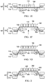
- FIGS. 1A-1G are cross sectional views of the major steps for singulating semiconductor dies using laser dicing.
- FIG. 2 is a cross section illustrating the singulation of dies on a semiconductor wafer by stretching dicing tape using a tape stretching table.
- FIG. 3 is a cross section illustrating the singulation of dies on a semiconductor wafer by stretching dicing tape using a tape stretching table.
- FIGS. 4A-4C are cross sectional views of the major steps for singulating semiconductor dies using wafer sawing.
- FIGS. 5A-5H are cross sectional views of the major steps for singulating semiconductor dies one from another using dicing tape on both sides of the semiconductor wafer.
- FIGS. 6A-6C are cross sectional views of the major steps for removing a second dicing tape with a light sensitive adhesive.
- FIG. 7 is a flow diagram illustrating a method such as the method of FIGS. 5A-5H .
- FIG. 8 is a flow diagram illustrating a method of forming a packaged semiconductor device for use with the method of FIG. 7 .
- FIG. 9 is a cross sectional view of a packaged semiconductor device.
- FIG. 10 is a projection view of a packaged semiconductor device.
- scribe lane is used herein.
- a scribe lane is a portion of semiconductor wafer between semiconductor dies.
- Sometimes in related literature the term “scribe street” is used.
- the semiconductor devices are separated into individual semiconductor dies by severing the semiconductor wafer along the scribe lanes. The separated dies can then be removed and handled individually for further processing including packaging. This process of removing dies from a wafer is referred to as “singulation” or sometimes referred to as “dicing.” Scribe lanes are arranged on four sides of semiconductor dies and when the dies are singulated from one another, rectangular semiconductor dies are formed.
- Coupled includes elements that are directly connected, and elements that are electrically connected even with intervening elements or wires are also coupled.
- a semiconductor die can be a discrete semiconductor device such as a bipolar transistor, a few discrete devices such as a pair of power FET switches fabricated together on a single semiconductor die, or a semiconductor die can be an integrated circuit with multiple semiconductor devices such as the multiple capacitors in an A/D converter.
- the semiconductor die can include passive devices such as resistors, inductors, filters, or active devices such as transistors.
- the semiconductor die can be an integrated circuit with hundreds or thousands of transistors coupled to form a functional circuit, for example a microprocessor or memory device.
- the semiconductor die can be a passive device such as a sensor, example sensors include photocells, transducers, and charge coupled devices (CCDs), or can be a micromechanical device, such as a digital micromirror device (DMD) or a MEMS device.
- a passive device such as a sensor
- sensors include photocells, transducers, and charge coupled devices (CCDs)
- CCDs charge coupled devices
- micromechanical device such as a digital micromirror device (DMD) or a MEMS device.
- stress induced dislocation is used herein.
- laser dicing laser energy is focused into particular locations within a semiconductor substrate. The laser energy melts a portion of the semiconductor material forming polysilicon regions. Because the polysilicon takes a larger area than the semiconductor crystal lattice, forming it induces stress and dislocates the semiconductor crystal lattice in the region affected by the laser energy, resulting in a stress induced dislocation in the semiconductor substrate.
- a mechanical sawing operation a saw blade is used to partially cut the semiconductor substrate, forming stress induced dislocations in the crystal lattice of the semiconductor substrate. When the substrate is then pulled on using a dicing tape, the stress induced dislocations can be propagated to form openings that eventually extend through the semiconductor substrate, the openings formed along the scribe lanes and thus forming rectangular semiconductor dies.
- FIGS. 1A through 1F are cross sectional views of the major manufacturing steps for singulating semiconductor dies.
- FIG. 1A shows a semiconductor wafer 100 positioned over a backgrinding tape 101 .
- Semiconductor devices 104 such as a resistors, capacitors, transistors, analog circuits, or integrated circuits, are built on and in the surface of the substrate 102 of the semiconductor wafer 100 .
- the semiconductor devices are separated from one another by scribe lanes (not shown in FIG. 1A ) that run between the semiconductor devices and intersect one another to surround each of the semiconductor devices 104 on four sides.
- FIG. 1B illustrates a laser dicing method in which a laser 110 is used to form stress induced dislocations 112 along defined scribe lanes in the semiconductor substrate 102 .
- this laser dicing method is referred to as a “stealth dicing” method because the laser is focused to affect regions within the semiconductor substrate, but does not cut through the entire substrate.
- the wafer assembly is loaded into a laser dicing tool.
- the wafer assembly can have the backgrinding tape 101 held by a vacuum chuck 131 and supported by a vacuum chuck support 135 .
- the wafer assembly is positioned with the non-device side (backside) of the semiconductor wafer 100 facing the laser 110 .
- Laser light is projected into the substrate 102 from the non-circuit side (backside) of the semiconductor wafer 100 forming stress induced dislocations 112 along the scribe lanes.
- the laser can be focused at particular depths in the semiconductor wafer to form stress induced dislocations 112 within the semiconductor wafer 100 .
- Multiple passes of laser energy focused at different depths can be used to form the stress induced dislocations 112 .
- a single pass can include more than one laser beam with different beams focused at more than one depth within the semiconductor substrate 102 to form stress induced dislocations 112 at the different depths.
- FIG. 1C a sticky side of a dicing tape 106 is adhered to the bottom surface (as oriented in FIG. 1B ) of a flexible dicing frame 108 .
- the semiconductor wafer 100 is positioned in the center of the dicing ring 108 and is adhered to a sticky side of the dicing tape 106 , forming a wafer dicing assembly 105 .
- the flexible dicing frame 108 supports the dicing tape 106 and the semiconductor wafer 100 in a dicing tool (not shown in FIG. 1B ).
- the dicing tool will operate to form openings in the semiconductor substrate along the scribe lanes between the semiconductor dies 103 (see FIG. 1F ).
- the frame 108 also supports the wafer dicing assembly 105 in the dicing tool.
- a dicing tape stretching table in the die singulation tool stretches the dicing tape 106 to separate the dies 103 from one another (see 118 in FIG. 1F ).
- FIG. 1C the backgrinding tape 101 is shown being peeled away from the wafer 100 and the devices 104 .
- the wafer dicing assembly 105 is loaded into a dicing tool 107 which consists of first clamps 114 and second clamps 116 for securing the wafer dicing assembly 105 in place.
- the non-sticky side of the dicing tape 106 faces the dicing tape stretching table 118 .
- the wafer 100 is mounted on the opposing sticky side of the dicing tape 106 .
- dicing tape stretching table 118 stretches the dicing tape 106 .
- the first clamp 114 and the second clamp 116 hold the flexible dicing frame 108 portion of the wafer dicing assembly 105 securely in place over the tape stretching table 118 .
- the non-sticky side of the dicing tape 106 faces the tape stretching table 118 .
- the dicing tape 106 is stretched in all directions, even though the cross sectional views show only a portion of the dicing tape and wafer that are visible in cross section, but the tape stretching tool 118 applies force in a circumference around the semiconductor wafer 100 and stretches the dicing tape 106 in all directions, causing the dies 103 to separate along the scribe lanes on all four sides of each die 103 , forming rectangular dies as the dies 103 separate from one another.
- the tape stretching table 118 is raised against the dicing tape 106 causing it to stretch.
- the force applied by the tape 106 as it stretches causes dislocations 112 to propagate completely through the semiconductor substrate 102 along the scribe lanes.
- the semiconductor dies 103 are separated one from another as gaps open between the semiconductor dies 103 along the scribe lanes, to singulate the dies 103 .
- the singulated semiconductor dies 103 are then removed from the dicing tape 106 . This can be done using pick and place equipment, for example.
- FIGS. 2 and 3 are cross-sectional views that illustrate issues that can arise in singulating semiconductor dies, particularly when the semiconductor dies have a thick layer of coating material or interconnect metal.
- substrate 202 in FIG. corresponds to substrate 102 in FIG. 1A .
- Dicing tool 207 has clamps 216 , 214 securing the ring 208 and the dicing tape 206 which carries semiconductor wafer 200 , including semiconductor devices 204 and substrate 202 .
- the thick layer of interconnect or passivation coating material over the semiconductor devices 204 can sometimes fail to crack apart and separate during singulation, resulting in bridged material ( 220 in FIG.
- the semiconductor dies 203 can fail to singulate when the top layer of interconnect has a thickness of 2-3 ⁇ m or greater and when the passivation coater material has a thickness of about 7 ⁇ m or greater. Singulation failure of the semiconductor dies results in costly scrap, increasing manufacturing costs.
- FIG. 3 illustrates another problem that can occur in singulating dies when semiconductor dies are relatively small, for example, dies with dimensions of 1 mm on a side, or less.
- substrate 302 in FIG. 3 corresponds to substrate 102 in FIG. 1A .
- Wafers manufactured with small dies have many more scribe lanes per wafer (compared to wafers with larger sized dies).
- the force applied by the stretching dicing tape 306 is therefore divided between many more scribe lanes.
- the force applied per scribe lane is thus significantly less for singulation on wafers with small dies than for similar wafers with larger dies.
- some of the small dies 303 can fail to singulate, leaving bridging material between dies 303 , shown as 320 . This also results in costly scrap.
- FIGS. 4A, 4B, and 4C illustrate an alternative method for singulating semiconductor dies.
- FIGS. 4A, 4B and 4C similar reference labels are used for similar elements as are shown in FIG. 1A .
- substrate 402 in FIGS. 4A, 4B and 4C corresponds to substrate 102 in FIG. 1A .
- FIG. 4A shows a wafer dicing assembly 405 consisting of a semiconductor wafer 400 mounted on the sticky side of dicing tape 406 .
- the sticky side of the dicing tape 406 is adhered to a dicing tape support ring 408 .
- the semiconductor wafer 400 is shown in FIG. 4A with the non-device side (substrate 402 ) of the wafer 400 adhered to the sticky side of the dicing tape 406 . This is optional.
- the device side 404 of the wafer 400 can instead be adhered to the sticky side of the dicing tape 406 .
- a dicing saw 422 can be used to form partial cuts 424 through the semiconductor wafer 400 to form stress induced dislocations along the scribe lanes.
- the partial cut 424 is at least half way through the semiconductor wafer 400 .
- the cut can extend from about 70% and up to 99% of the wafer.
- a laser saw can be used to cut into the surface of the semiconductor wafer at least half way through.
- FIG. 4B the wafer dicing assembly 405 is shown clamped between a first clamp 414 and a second clamp 416 in a dicing tool.
- the clamps 414 , 416 are used to position the mounted wafer assembly 407 over the dicing tape stretching table 418 .
- FIG. 4C illustrates the dicing tape stretching table 418 in operation.
- the dicing tape stretching table 418 is raised against the non-sticky surface of the dicing tape 406 in the wafer dicing assembly 407 and pushes against the dicing tape 406 , causing it to stretch.
- the force applied by the stretching dicing tape 406 causes the cuts 424 to propagate completely through the semiconductor substrate 402 .
- the semiconductor dies 403 are separated from one another as gaps open between semiconductor dies 403 . Then, singulated semiconductor dies 403 are removed from the dicing tape 406 .
- the cross sectional views show the dicing tape stretching table 418 contacting the dicing tape 406 at two positions that are visible in the cross sectional view of FIGS. 4B-4C
- the dicing tape stretching tool 418 contacts the dicing tape 406 in a circular pattern around the semiconductor substrate 402 , and as the force is applied, the tape 406 is stretched in all directions.
- the stress induced dislocations caused by the cuts in the scribe lanes on each side of the semiconductor dies propagate through the substrate and form openings due to the force applied to stretch the dicing tape 406 , and the force applied by the stretched dicing tape 406 pulls the semiconductor dies 403 apart to form rectangular dies.
- FIGS. 5A through 5H illustrate the major steps in an example method.
- similar reference labels are used for similar elements as are shown in FIG. 1A .
- substrate 502 in FIGS. 5A through 5H corresponds to substrate 102 in FIG. 1A .
- FIG. 7 is a process flow that describes the manufacturing steps illustrated in FIGS. 5A through 5H .
- FIG. 5A shows a substrate 502 with devices 504 is mounted on a backgrinding tape 501 and being subjected to a laser dicing process (sometimes referred to as a “stealth dicing” process) from the backside.
- Backgrinding tape 501 is positioned on a vacuum chuck 531 which is on a support 535 that supports the substrate 502 .
- Laser 510 is scanned across the substrate 502 and forms stress induced dislocation regions 512 in scribe lanes.
- a dicing tape 506 and a flexible dicing frame 508 form a wafer dicing assembly 505 .
- the dicing tape 506 can be one of many dicing tapes that are commercially available, but in a particular example process the tape 506 is type UE-110BJ from Nitto Denko Corporation, and has a thickness of about 105 ⁇ m.
- the wafer dicing assembly 505 is formed (step 701 , FIG. 7 ) by adhering the sticky side of a first dicing tape 506 to a first surface of the dicing ring 508 .
- the backside of a semiconductor wafer is positioned in the center of the dicing ring 508 and is adhered to the sticky side of the first dicing tape 506 forming the wafer dicing assembly 505 .
- the dicing ring 508 supports the first dicing tape 506 and the semiconductor wafer 500 in the dicing tool.
- the semiconductor wafer includes substrate 502 and semiconductor devices 504 .
- the backgrinding tape 501 is shown being peeled away from the substrate 502 .
- the sticky side of a second dicing tape 526 is shown adhered to the second side of the semiconductor device wafer 500 and to the second side of the dicing ring 508 .
- the second dicing tape 526 can be one of many dicing tapes that are commercially available, and can be the same type of dicing tape as 506 , or can be a different type.
- the second dicing tape needs to be peelable or otherwise removable from the assembly in later steps.
- the second dicing tape was type UE-111AJ, from Nitto Denko Corporation, with a thickness of about 107 ⁇ m.
- the second dicing tape 526 is adhered to the sticky side of the first dicing tape 506 . Adhering the tapes to one another keeps the two tapes stretching together at the same rate in a stretching step described hereinbelow.
- the double taped wafer dicing assembly 509 is shown loaded into a dicing tool 507 in FIG. 5D (step 709 ), and is positioned over a tape stretching table 518 .
- FIG. 5E shows the dicing ring 508 is clamped between a first clamp 514 against the first dicing tape 506 and the first side of the dicing ring 508 and a second clamp 516 against the second dicing tape 526 and the second side of the dicing ring 508 .
- the clamps 514 and 516 hold the double taped wafer dicing assembly 509 in place above the tape stretching table 518 .
- FIG. 5F shows the tape stretching table 518 being raised against the non-sticky side of the first dicing tape 506 , causing the first dicing tape 506 and the second dicing tape 526 to stretch simultaneously together.
- force is applied by the stretching dicing tapes, causing stress induced dislocations 512 to propagate within the substrate along the scribe lanes and eventually forming openings that extend completely through the semiconductor substrate 502 .
- the semiconductor dies are separated as the stress induced dislocations become open gaps between semiconductor dies 503 . Note that the stretching force is applied in all directions by the dicing tape stretching tool 518 , so that the gaps propagate in the scribe lanes on all four sides of the semiconductor dies 503 .
- FIG. 5G shows the second clamp 516 released from against the second dicing tape 526 and the second dicing tape 526 being removed.
- the second dicing tape 526 is mechanically peeled from the assembly 509 , while the first dicing tape 506 remains in place, supporting the semiconductor dies 503 .
- step 717 the singulated dies 503 are shown being removed from the first dicing tape 506 . This can be done, for example, using pick and place tools.
- the second dicing tape 526 applies additional force (compared to a single dicing tape system) to the stress induced dislocations 512 between the dies 503 as the tapes stretch.
- the force applied to the wafer approximately doubles using the arrangements with dual dicing tapes (when compared to a single dicing tape.)
- the additional force applied eliminates the bridging between semiconductor dies 503 (see 220 , FIG. 2 ) that sometimes prevents dies ( 203 in FIG. 2 ) from singulating on wafers with a thick top metal or a thick top coating material.
- the second dicing tape 526 also eliminates dies (see 303 , FIG. 3 ) that fail to singulate on wafers with small dies of less than 1 mm dimension. Use of the arrangements increases overall die yield. Yield is especially increased for semiconductor dies such as 503 with a thick interconnect metal or topcoat. Yield is also especially increased for semiconductor wafers with small (less than about 1 mm) die size.
- FIGS. 6A-6C illustrate in a series of cross sections an alternative example method for removing the second dicing tape 626 after stretching and die separation.
- similar reference labels are used for similar elements as are shown in FIG. 1A .
- substrate 602 corresponds to substrate 102 in FIG. 1A .
- the adhesive on the second dicing tape 626 is light sensitive. Upon exposure to light, this light sensitive adhesive loses its adhesive properties. This can be referred to as “UV-release” dicing tape, or “photo-release” dicing tape. Although UV release dicing tape is commonly used, other light frequencies can also be used.
- step 713 , FIG. 7 assembly 609 is shown with substrate 602 between dicing tapes 626 and 606 in dicing tool 607 . Outside of the circumference of the wafer the two dicing tapes are adhered to one another, to assure that when stretched, the two tapes stretch together.
- the assembly 609 is shown after separation of the dies 603 (see FIG. 5F , for example).
- the cross section shows a light source 628 that exposes the light sensitive adhesive on the second dicing tape 626 .
- it can be UV light.
- the type of light applied is determined by the tape adhesive used.
- FIG. 6B shows the second dicing tape 626 now easily removed from the dies 603 , since the second dicing tape 626 no longer adheres to the dies 603 .
- FIG. 6C shows the individual dies 603 being removed from the first dicing tape 606 .
- dies 503 may adhere to the second dicing tape 526 when it is removed.
- the use of the light sensitive release second dicing tape 626 eliminates this issue.
- Alternative tape types can be used in the arrangements.
- the second dicing tape is removed, while the singulated dies remain on the first dicing tape.
- the first tape can be removed while the singulated dies remain on the second dicing tape.
- Other tape types can be used in additional alternatives that enable removal of one of the two dicing tapes while the other tape remains in place.
- Light sensitive tape including UV release tape, can be used as described herein.
- light sensitive release dicing tape can be used for both the first and second dicing tapes.
- the first dicing tape can also be light or UV sensitive for release, and light can expose the backside of the first dicing tape after the second dicing tape has been removed, making picking the semiconductor dies from the first tape easier to perform.
- Other arrangements can use tape that is not light sensitive or that releases the adhesive in response to a chemical treatment, or that is simply mechanically removed as shown hereinabove.
- FIG. 8 is a flow diagram that illustrates a method for packaging the semiconductor dies to form packaged semiconductor devices.
- step 801 semiconductor dies are formed on a semiconductor wafer spaced from one another by scribe lanes.
- step 803 the semiconductor dies are separated from one another using either the laser dicing, mechanical sawing, or laser sawing processes described above, and using the dual dicing tapes that are stretched at the same time to separate the dies along the scribe lanes as described above.
- the dies are then singulated and pick and place operations remove the semiconductor dies from the dicing tapes as described above.
- the semiconductor dies are mounted on a substrate.
- the substrate can be conductive metal lead frames in a lead frame strip.
- a lead frame strip includes several lead frames, each having leads and a die mount area supported by removable portions of the lead frame strip.
- Materials for lead frames include copper and alloys of copper, copper plated nickel or other base material, Alloy 42, stainless steel, other conductive materials. Bondable or solderable coatings such as nickel, palladium, tin, solder, combinations of these, or other coatings can be formed over the substrate to aid in making solder or wire bond connections to the leads of the substrate.
- molded interconnect substrates with conductors formed in a matrix with dielectric material such as mold compound or epoxy, or a partially etched or “half-etched” metal substrate.
- PMLF Premolded lead frame
- the semiconductor dies are placed on die mount areas of the substrate. In an example process several die mount areas are provided in an array or matrix for forming several packages simultaneously, using the substrate that is provided as an array or strip. In a flip-chip method, the semiconductor die is placed with the active circuitry facing the substrate strip.
- Solder bumps or pillar bumps on bond pads of the semiconductor die are placed in contact with portions of the leads in the substrate, and solder reflow is performed to electrically connect and mechanically bond the solder bumps or pillar bumps to the leads.
- solder reflow is performed to electrically connect and mechanically bond the solder bumps or pillar bumps to the leads.
- the semiconductor die is placed with the active circuitry facing away from the substrate strip. Bond wires are attached to bond pads of the semiconductor dies and to lead portions of the leads of the substrate to electrically connect the semiconductor dies to the leads. If the substrate is a lead frame, removable portions of the lead frame keep the leads in place during packaging, these removable portions are then trimmed away after the die is mounted, bonded and covered with a dielectric material such as mold compound.
- a mold compound is applied over the semiconductor dies.
- the mold compound covers the semiconductor die and at least portions of the substrate strip. Portions of the leads are also not covered with mold compound so that these portions can later be used to make electrical connections to the packaged semiconductor device.
- a liquid mold compound can be applied over the semiconductor die and portions of the substrate, and then cured to form a package body.
- a thermoset plastic resin can be provided as a solid, heated to a liquid state, pressed into a mold containing the substrate strip, and then cured to form a solid package.
- Room temperature liquid material such as resins, epoxies and polymers, can be applied and cured simply using time or by applying UV or thermal energy to become cured and form a solid package.
- the packaged semiconductor dies and lead frames are singulated from one another by cutting between the lead frames in saw streets in the substrate strip. If the mold compound also covers the saw street areas (for example in a “block molding” process), the mold compound is also cut through to singulate the packaged semiconductor devices from one another.
- FIG. 9 is a cross sectional view of an example packaged semiconductor device 954 that can be formed by the process steps of FIG. 8 as described above.
- a wire bonded semiconductor die 902 is shown packaged in a quad flat no-leads (QFN) package.
- Semiconductor die 902 is mounted on a die mount area 942 of a lead frame or other substrate 940 .
- Leads 944 of substrate 940 are coupled to the bond pads 960 on the semiconductor die 902 by bond wires 958 .
- a protective overcoat layer 956 covers the conductors 910 on the active device side of the semiconductor die on substrate 902 , and openings in the protective overcoat layer 956 expose the bond pads 960 for bonding.
- a dielectric layer 904 is shown on the active surface of semiconductor substrate 902 , in a practical example layer 904 may have several layers and conductors 910 may also have several layers that are electrically insulated from one another by additional dielectric layers such as 904 , and with vias extending between the conductor layers and extending through the dielectric layers that provide electrical connections between the conductor layers.
- Mold compound 952 covers the semiconductor die 902 , the bond wires 958 , and portions of substrate 940 , while portions of leads 944 are left uncovered with mold compound. The uncovered portions of leads 944 enable electrical connection to the packaged semiconductor device 954 .
- FIG. 10 is a projection view of a quad flat no leads (QFN) packaged semiconductor device 1054 that similar to the packaged semiconductor device 954 in FIG. 9 .
- the packaged semiconductor device is formed by the mold compound with portions of leads 1044 exposed from the mold compound to form electrical terminals for the packaged semiconductor device 1054 .
- Other packages can be used with the arrangements including ball grid array (BGA) packages, small outline packages with leads or small outline no lead (SON) packages, and other leaded and no lead semiconductor packages can be used with the arrangements.
- BGA ball grid array
- SON small outline no lead
Abstract
In a described example, a method includes: forming stress induced dislocations along scribe lanes between semiconductor dies on a semiconductor wafer using a laser; mounting a first side of the semiconductor wafer on the first side of a first dicing tape; removing a backgrinding tape from the semiconductor wafer; attaching a second dicing tape to a second side of the semiconductor wafer opposite the first side, the second dicing tape adhering to portions of the first dicing tape that are spaced from the semiconductor wafer, forming a dual taped wafer dicing assembly; separating the semiconductor dies by stretching the first dicing tape and stretching the second dicing tape; removing the second dicing tape from the semiconductor dies; and removing the semiconductor dies from the first dicing tape.
Description
This application claims the benefit under 35 U.S.C. § 119(e) to co-owned U.S. Provisional Patent Application Ser. No. 62/787,105, filed Dec. 31, 2018, titled “SEMICONDUCTOR DIE SINGULATION, which is hereby incorporated herein by reference.
This disclosure relates generally to semiconductor dies, and more particularly to a method of semiconductor die singulation.
In a described example, a method includes: mounting a device side of a semiconductor wafer on a first side of a backgrinding tape; loading the backgrinding tape and semiconductor wafer into a dicing tool; forming stress induced dislocations along scribe lanes between semiconductor dies on the semiconductor wafer using a laser in the dicing tool. The method continues by attaching an adhesive on a first side of a first dicing tape to a first side of a dicing ring; mounting a first side of the semiconductor wafer on the first side of the first dicing tape, forming a wafer dicing assembly; removing the backgrinding tape from the semiconductor wafer; attaching a first side of a second dicing tape that has an adhesive to a second side of the semiconductor wafer opposite the first side, the second dicing tape adhering to portions of the first dicing tape that are spaced from the semiconductor wafer; and adhering the second dicing tape to a second side of the dicing ring, forming a dual taped wafer dicing assembly. The dual taped wafer dicing assembly is loaded into a die singulation tool with a dicing tape stretching table; the method then separates the semiconductor dies by stretching the first dicing tape and stretching the second dicing tape with the dicing tape stretching table; and the method continues by removing the second dicing tape from the semiconductor dies; and removing the semiconductor dies from the first dicing tape. In additional example methods, the singulated semiconductor dies are packaged to form packaged semiconductor devices.
Corresponding numerals and symbols in the different figures generally refer to corresponding parts, unless otherwise indicated. The figures are not necessarily drawn to scale.
The term “scribe lane” is used herein. A scribe lane is a portion of semiconductor wafer between semiconductor dies. Sometimes in related literature the term “scribe street” is used. Once processing is finished and the semiconductor devices are complete, the semiconductor devices are separated into individual semiconductor dies by severing the semiconductor wafer along the scribe lanes. The separated dies can then be removed and handled individually for further processing including packaging. This process of removing dies from a wafer is referred to as “singulation” or sometimes referred to as “dicing.” Scribe lanes are arranged on four sides of semiconductor dies and when the dies are singulated from one another, rectangular semiconductor dies are formed.
Elements are described herein as “coupled.” As used herein, the term “coupled” includes elements that are directly connected, and elements that are electrically connected even with intervening elements or wires are also coupled.
The term “semiconductor die” is used herein. A semiconductor die can be a discrete semiconductor device such as a bipolar transistor, a few discrete devices such as a pair of power FET switches fabricated together on a single semiconductor die, or a semiconductor die can be an integrated circuit with multiple semiconductor devices such as the multiple capacitors in an A/D converter. The semiconductor die can include passive devices such as resistors, inductors, filters, or active devices such as transistors. The semiconductor die can be an integrated circuit with hundreds or thousands of transistors coupled to form a functional circuit, for example a microprocessor or memory device. The semiconductor die can be a passive device such as a sensor, example sensors include photocells, transducers, and charge coupled devices (CCDs), or can be a micromechanical device, such as a digital micromirror device (DMD) or a MEMS device.
The term “stress induced dislocation” is used herein. In laser dicing, laser energy is focused into particular locations within a semiconductor substrate. The laser energy melts a portion of the semiconductor material forming polysilicon regions. Because the polysilicon takes a larger area than the semiconductor crystal lattice, forming it induces stress and dislocates the semiconductor crystal lattice in the region affected by the laser energy, resulting in a stress induced dislocation in the semiconductor substrate. In a mechanical sawing operation, a saw blade is used to partially cut the semiconductor substrate, forming stress induced dislocations in the crystal lattice of the semiconductor substrate. When the substrate is then pulled on using a dicing tape, the stress induced dislocations can be propagated to form openings that eventually extend through the semiconductor substrate, the openings formed along the scribe lanes and thus forming rectangular semiconductor dies.
In FIG. 1B , illustrates a laser dicing method in which a laser 110 is used to form stress induced dislocations 112 along defined scribe lanes in the semiconductor substrate 102. (In some literature, this laser dicing method is referred to as a “stealth dicing” method because the laser is focused to affect regions within the semiconductor substrate, but does not cut through the entire substrate. In the laser dicing method, the wafer assembly is loaded into a laser dicing tool. In an example method, the wafer assembly can have the backgrinding tape 101 held by a vacuum chuck 131 and supported by a vacuum chuck support 135. The wafer assembly is positioned with the non-device side (backside) of the semiconductor wafer 100 facing the laser 110. Laser light is projected into the substrate 102 from the non-circuit side (backside) of the semiconductor wafer 100 forming stress induced dislocations 112 along the scribe lanes. The laser can be focused at particular depths in the semiconductor wafer to form stress induced dislocations 112 within the semiconductor wafer 100. Multiple passes of laser energy focused at different depths can be used to form the stress induced dislocations 112. A single pass can include more than one laser beam with different beams focused at more than one depth within the semiconductor substrate 102 to form stress induced dislocations 112 at the different depths.
In FIG. 1C a sticky side of a dicing tape 106 is adhered to the bottom surface (as oriented in FIG. 1B ) of a flexible dicing frame 108. The semiconductor wafer 100 is positioned in the center of the dicing ring 108 and is adhered to a sticky side of the dicing tape 106, forming a wafer dicing assembly 105. The flexible dicing frame 108 supports the dicing tape 106 and the semiconductor wafer 100 in a dicing tool (not shown in FIG. 1B ). The dicing tool will operate to form openings in the semiconductor substrate along the scribe lanes between the semiconductor dies 103 (see FIG. 1F ). The frame 108 also supports the wafer dicing assembly 105 in the dicing tool. A dicing tape stretching table in the die singulation tool stretches the dicing tape 106 to separate the dies 103 from one another (see 118 in FIG. 1F ). In FIG. 1C , the backgrinding tape 101 is shown being peeled away from the wafer 100 and the devices 104.
As illustrated in FIG. 1D the wafer dicing assembly 105 is loaded into a dicing tool 107 which consists of first clamps 114 and second clamps 116 for securing the wafer dicing assembly 105 in place. The non-sticky side of the dicing tape 106 faces the dicing tape stretching table 118. The wafer 100 is mounted on the opposing sticky side of the dicing tape 106. When the dicing tool is operated, dicing tape stretching table 118 stretches the dicing tape 106.
As illustrated in FIG. 1E , the first clamp 114 and the second clamp 116 hold the flexible dicing frame 108 portion of the wafer dicing assembly 105 securely in place over the tape stretching table 118. The non-sticky side of the dicing tape 106 faces the tape stretching table 118. Note that the dicing tape 106 is stretched in all directions, even though the cross sectional views show only a portion of the dicing tape and wafer that are visible in cross section, but the tape stretching tool 118 applies force in a circumference around the semiconductor wafer 100 and stretches the dicing tape 106 in all directions, causing the dies 103 to separate along the scribe lanes on all four sides of each die 103, forming rectangular dies as the dies 103 separate from one another.
As illustrated in FIG. 1F , the tape stretching table 118 is raised against the dicing tape 106 causing it to stretch. The force applied by the tape 106 as it stretches causes dislocations 112 to propagate completely through the semiconductor substrate 102 along the scribe lanes. As the dicing tape 106 is additionally stretched, the semiconductor dies 103 are separated one from another as gaps open between the semiconductor dies 103 along the scribe lanes, to singulate the dies 103.
As illustrated in FIG. 1G , the singulated semiconductor dies 103 are then removed from the dicing tape 106. This can be done using pick and place equipment, for example.
In FIG. 4A shows a wafer dicing assembly 405 consisting of a semiconductor wafer 400 mounted on the sticky side of dicing tape 406. In this example, the sticky side of the dicing tape 406 is adhered to a dicing tape support ring 408. The semiconductor wafer 400 is shown in FIG. 4A with the non-device side (substrate 402) of the wafer 400 adhered to the sticky side of the dicing tape 406. This is optional. In an alternative approach using a wafer sawing method, the device side 404 of the wafer 400 can instead be adhered to the sticky side of the dicing tape 406. A dicing saw 422 can be used to form partial cuts 424 through the semiconductor wafer 400 to form stress induced dislocations along the scribe lanes. In an example arrangement the partial cut 424 is at least half way through the semiconductor wafer 400. In additional examples the cut can extend from about 70% and up to 99% of the wafer. In an alternative to a mechanical sawing, a laser saw can be used to cut into the surface of the semiconductor wafer at least half way through.
In FIG. 4B the wafer dicing assembly 405 is shown clamped between a first clamp 414 and a second clamp 416 in a dicing tool. The clamps 414, 416 are used to position the mounted wafer assembly 407 over the dicing tape stretching table 418.
In FIG. 5B , a dicing tape 506 and a flexible dicing frame 508 form a wafer dicing assembly 505. The dicing tape 506 can be one of many dicing tapes that are commercially available, but in a particular example process the tape 506 is type UE-110BJ from Nitto Denko Corporation, and has a thickness of about 105 μm. The wafer dicing assembly 505 is formed (step 701, FIG. 7 ) by adhering the sticky side of a first dicing tape 506 to a first surface of the dicing ring 508. The backside of a semiconductor wafer is positioned in the center of the dicing ring 508 and is adhered to the sticky side of the first dicing tape 506 forming the wafer dicing assembly 505. The dicing ring 508 supports the first dicing tape 506 and the semiconductor wafer 500 in the dicing tool. The semiconductor wafer includes substrate 502 and semiconductor devices 504. In FIG. 5B , the backgrinding tape 501 is shown being peeled away from the substrate 502.
In FIG. 5C (step 707, FIG. 7 ) the sticky side of a second dicing tape 526 is shown adhered to the second side of the semiconductor device wafer 500 and to the second side of the dicing ring 508. This forms a double taped wafer dicing assembly 509. The second dicing tape 526 can be one of many dicing tapes that are commercially available, and can be the same type of dicing tape as 506, or can be a different type. The second dicing tape needs to be peelable or otherwise removable from the assembly in later steps. In an example, the second dicing tape was type UE-111AJ, from Nitto Denko Corporation, with a thickness of about 107 μm. In an area outside of the circumference of wafer 500, the second dicing tape 526 is adhered to the sticky side of the first dicing tape 506. Adhering the tapes to one another keeps the two tapes stretching together at the same rate in a stretching step described hereinbelow.
The double taped wafer dicing assembly 509 is shown loaded into a dicing tool 507 in FIG. 5D (step 709), and is positioned over a tape stretching table 518.
In FIG. 5H (step 717) the singulated dies 503 are shown being removed from the first dicing tape 506. This can be done, for example, using pick and place tools.
The second dicing tape 526 applies additional force (compared to a single dicing tape system) to the stress induced dislocations 512 between the dies 503 as the tapes stretch. The force applied to the wafer approximately doubles using the arrangements with dual dicing tapes (when compared to a single dicing tape.) The additional force applied eliminates the bridging between semiconductor dies 503 (see 220, FIG. 2 ) that sometimes prevents dies (203 in FIG. 2 ) from singulating on wafers with a thick top metal or a thick top coating material. The second dicing tape 526 also eliminates dies (see 303, FIG. 3 ) that fail to singulate on wafers with small dies of less than 1 mm dimension. Use of the arrangements increases overall die yield. Yield is especially increased for semiconductor dies such as 503 with a thick interconnect metal or topcoat. Yield is also especially increased for semiconductor wafers with small (less than about 1 mm) die size.
In this arrangement, the adhesive on the second dicing tape 626 is light sensitive. Upon exposure to light, this light sensitive adhesive loses its adhesive properties. This can be referred to as “UV-release” dicing tape, or “photo-release” dicing tape. Although UV release dicing tape is commonly used, other light frequencies can also be used.
In FIG. 6A , (step 713, FIG. 7 ) assembly 609 is shown with substrate 602 between dicing tapes 626 and 606 in dicing tool 607. Outside of the circumference of the wafer the two dicing tapes are adhered to one another, to assure that when stretched, the two tapes stretch together. The assembly 609 is shown after separation of the dies 603 (see FIG. 5F , for example). In FIG. 6A , the cross section shows a light source 628 that exposes the light sensitive adhesive on the second dicing tape 626. For example, it can be UV light. The type of light applied is determined by the tape adhesive used.
When the same type of dicing tape is used for both the first dicing tape 506 (see FIG. 5 ) and the second dicing tape 526, dies 503 may adhere to the second dicing tape 526 when it is removed. The use of the light sensitive release second dicing tape 626 (see FIG. 6 ) eliminates this issue.
Alternative tape types can be used in the arrangements. In the example arrangements, after singulation as described hereinabove, the second dicing tape is removed, while the singulated dies remain on the first dicing tape. In an alternative method, the first tape can be removed while the singulated dies remain on the second dicing tape. Other tape types can be used in additional alternatives that enable removal of one of the two dicing tapes while the other tape remains in place. Light sensitive tape, including UV release tape, can be used as described herein. In an alternative, light sensitive release dicing tape can be used for both the first and second dicing tapes. In a further alternative, the first dicing tape can also be light or UV sensitive for release, and light can expose the backside of the first dicing tape after the second dicing tape has been removed, making picking the semiconductor dies from the first tape easier to perform. Other arrangements can use tape that is not light sensitive or that releases the adhesive in response to a chemical treatment, or that is simply mechanically removed as shown hereinabove.
In step 801, semiconductor dies are formed on a semiconductor wafer spaced from one another by scribe lanes.
In step 803, the semiconductor dies are separated from one another using either the laser dicing, mechanical sawing, or laser sawing processes described above, and using the dual dicing tapes that are stretched at the same time to separate the dies along the scribe lanes as described above. The dies are then singulated and pick and place operations remove the semiconductor dies from the dicing tapes as described above.
At step 805, the semiconductor dies are mounted on a substrate. In one example the substrate can be conductive metal lead frames in a lead frame strip. A lead frame strip includes several lead frames, each having leads and a die mount area supported by removable portions of the lead frame strip. Materials for lead frames include copper and alloys of copper, copper plated nickel or other base material, Alloy 42, stainless steel, other conductive materials. Bondable or solderable coatings such as nickel, palladium, tin, solder, combinations of these, or other coatings can be formed over the substrate to aid in making solder or wire bond connections to the leads of the substrate. Other substrates that can be used include molded interconnect substrates (MIS) with conductors formed in a matrix with dielectric material such as mold compound or epoxy, or a partially etched or “half-etched” metal substrate. Premolded lead frame (PMLF) substrates can be used. The semiconductor dies are placed on die mount areas of the substrate. In an example process several die mount areas are provided in an array or matrix for forming several packages simultaneously, using the substrate that is provided as an array or strip. In a flip-chip method, the semiconductor die is placed with the active circuitry facing the substrate strip. Solder bumps or pillar bumps on bond pads of the semiconductor die are placed in contact with portions of the leads in the substrate, and solder reflow is performed to electrically connect and mechanically bond the solder bumps or pillar bumps to the leads. In a wire bond method, the semiconductor die is placed with the active circuitry facing away from the substrate strip. Bond wires are attached to bond pads of the semiconductor dies and to lead portions of the leads of the substrate to electrically connect the semiconductor dies to the leads. If the substrate is a lead frame, removable portions of the lead frame keep the leads in place during packaging, these removable portions are then trimmed away after the die is mounted, bonded and covered with a dielectric material such as mold compound.
At step 807, a mold compound is applied over the semiconductor dies. The mold compound covers the semiconductor die and at least portions of the substrate strip. Portions of the leads are also not covered with mold compound so that these portions can later be used to make electrical connections to the packaged semiconductor device. In an encapsulation molding process a liquid mold compound can be applied over the semiconductor die and portions of the substrate, and then cured to form a package body. A thermoset plastic resin can be provided as a solid, heated to a liquid state, pressed into a mold containing the substrate strip, and then cured to form a solid package. Room temperature liquid material, such as resins, epoxies and polymers, can be applied and cured simply using time or by applying UV or thermal energy to become cured and form a solid package.
At step 809, the packaged semiconductor dies and lead frames are singulated from one another by cutting between the lead frames in saw streets in the substrate strip. If the mold compound also covers the saw street areas (for example in a “block molding” process), the mold compound is also cut through to singulate the packaged semiconductor devices from one another.
Modifications and variations are contemplated and can be made in the described arrangements, and other alternative arrangements are possible that are within the scope of the claims.
Claims (26)
1. A method for making a semiconductor device, comprising:
forming stress induced dislocations in scribe lanes between semiconductor dies on a semiconductor wafer;
mounting a first side of the semiconductor wafer on a first side of a first dicing tape having an adhesive, forming a wafer dicing assembly;
attaching a first side of a second dicing tape that has an adhesive to a second side of the semiconductor wafer and to the first side of the first dicing tape in portions of the first dicing tape spaced from the semiconductor wafer;
separating the semiconductor dies one from another by simultaneously stretching the first dicing tape and stretching the second dicing tape to open gaps in the scribe lanes by extending the stress induced dislocations formed in the semiconductor wafer in the scribe lanes;
removing the second dicing tape from the semiconductor dies which are now singulated dies spaced from one another;
removing the singulated semiconductor dies from the first dicing tape;
positioning singulated semiconductor dies on die mount portions of a substrate in a substrate strip;
coupling leads of the substrate to bond pads on the semiconductor dies;
covering the semiconductor dies and at least a portion of the leads in mold compound;
cutting the substrate strip and the mold compound along saw streets to separate the semiconductor dies covered in mold compound and mounted to the substrate, forming separate packaged semiconductor devices each including a semiconductor die.
2. The method of claim 1 , wherein the packaged semiconductor device forms a quad flat no lead (QFN) packaged device.
3. The method of claim 1 , wherein the packaged semiconductor device forms a small outline no lead (SON) package.
4. The method of claim 1 , wherein the first dicing tape and the second dicing tape are the same type of dicing tape.
5. The method of claim 1 , wherein the first dicing tape is a different type than the second dicing tape.
6. The method of claim 1 , wherein the adhesive on the first side of the second dicing tape is light sensitive and further comprising exposing the adhesive of the second tape to light prior to removing the second tape.
7. The method of claim 6 , wherein the light is ultraviolet (UV) light.
8. The method of claim 1 wherein prior to applying the first dicing tape, the semiconductor wafer is placed into a laser dicing tool, and laser dicing is performed to form the stress induced dislocations in the semiconductor wafer in the scribe lanes.
9. The method of claim 1 wherein prior to attaching the second dicing tape, the wafer dicing assembly is placed into a wafer sawing tool and the wafer sawing tool cuts through a portion of the semiconductor wafer along scribe lanes, forming the stress induced dislocations in the semiconductor wafer.
10. The method of claim 9 , wherein the portion is at least half a thickness of the semiconductor wafer.
11. A method of making a semiconductor device, comprising:
mounting a device side of a semiconductor wafer on a first side of a backgrinding tape;
loading the backgrinding tape and semiconductor wafer into a dicing tool;
forming stress induced dislocations along scribe lanes between semiconductor dies on the semiconductor wafer using a laser in the dicing tool;
attaching an adhesive on a first side of a first dicing tape to a first side of a dicing ring;
mounting a first side of the semiconductor wafer on the first side of the first dicing tape, forming a wafer dicing assembly;
removing the backgrinding tape from the semiconductor wafer;
attaching a first side of a second dicing tape that has an adhesive to a second side of the semiconductor wafer opposite the first side, the second dicing tape adhering to portions of the first dicing tape that are spaced from the semiconductor wafer;
adhering the second dicing tape to a second side of the dicing ring, forming a dual taped wafer dicing assembly;
loading the dual taped wafer dicing assembly into a die singulation tool with a dicing tape stretching table;
separating the semiconductor dies by stretching the first dicing tape and stretching the second dicing tape with the dicing tape stretching table;
removing the second dicing tape from the semiconductor dies; and
removing the semiconductor dies from the first dicing tape.
12. The method of claim 11 , wherein the first dicing tape and the second dicing tape are a same type of dicing tape.
13. The method of claim 11 , wherein the first dicing tape is different than the second dicing tape.
14. The method of claim 11 , wherein the adhesive on the second dicing tape is light sensitive and further comprising exposing the second adhesive to light prior to removing the second dicing tape.
15. The method of claim 14 , wherein the light is ultraviolet (UV) light.
16. The method of claim 11 , wherein the semiconductor dies are square and have a dimension of less than 1 mm per side.
17. The method of claim 11 , wherein the semiconductor wafer has a top metal layer that is greater than 2 μms thick.
18. The method of claim 11 , wherein the semiconductor wafer has a passivation coating greater than 7 μms thick.
19. A method for making a semiconductor device, comprising:
adhering a first side of a first dicing tape that has an adhesive to a first side of a dicing ring;
mounting a first side of a semiconductor wafer on the first side of the first dicing tape, the semiconductor wafer having semiconductor dies spaced by scribe lanes between the semiconductor dies;
partially cutting through the semiconductor wafer along scribe lanes;
adhering a first side of a second dicing tape with a light sensitive adhesive to a second side of the semiconductor wafer and to portions of the first dicing tape spaced from the semiconductor wafer;
adhering the first side of the second dicing tape to a second side of the dicing ring, forming a dual taped wafer dicing assembly;
loading the dual taped wafer dicing assembly into a dicing tool with a dicing tape stretching table;
separating the semiconductor dies from the wafer and from one another by stretching the first dicing tape and stretching the second dicing tape with the dicing tape stretching table, expanding the cuts in the semiconductor wafer along the scribe lanes between the semiconductor dies;
exposing the light sensitive adhesive to light;
removing the second dicing tape from the semiconductor dies; and
removing the semiconductor dies from the first dicing tape.
20. The method of claim 19 , wherein the light is ultraviolet (UV) light.
21. The method of claim 19 , and further comprising exposing the first dicing tape to light after the second dicing tape is removed, where the first dicing tape is a light release dicing tape.
22. The method of claim 21 , wherein the light is UV light.
23. The method of claim 19 , wherein the first side is a device side of the semiconductor wafer.
24. The method of claim 19 , wherein the first side is a non-device side of the semiconductor wafer.
25. The method of claim 19 , wherein the partially cutting is performed by sawing.
26. The method of claim 19 , wherein the partially cutting is performed by laser cutting.
Priority Applications (1)
| Application Number | Priority Date | Filing Date | Title |
|---|---|---|---|
| US16/291,995 US10658240B1 (en) | 2018-12-31 | 2019-03-04 | Semiconductor die singulation |
Applications Claiming Priority (2)
| Application Number | Priority Date | Filing Date | Title |
|---|---|---|---|
| US201862787105P | 2018-12-31 | 2018-12-31 | |
| US16/291,995 US10658240B1 (en) | 2018-12-31 | 2019-03-04 | Semiconductor die singulation |
Publications (1)
| Publication Number | Publication Date |
|---|---|
| US10658240B1 true US10658240B1 (en) | 2020-05-19 |
Family
ID=70736507
Family Applications (1)
| Application Number | Title | Priority Date | Filing Date |
|---|---|---|---|
| US16/291,995 Active US10658240B1 (en) | 2018-12-31 | 2019-03-04 | Semiconductor die singulation |
Country Status (1)
| Country | Link |
|---|---|
| US (1) | US10658240B1 (en) |
Cited By (3)
| Publication number | Priority date | Publication date | Assignee | Title |
|---|---|---|---|---|
| US20210375834A1 (en) * | 2018-10-24 | 2021-12-02 | Aledia | Electronic device |
| US20220044970A1 (en) * | 2020-08-10 | 2022-02-10 | Disco Corporation | Method of processing a substrate |
| US11315821B2 (en) * | 2019-08-29 | 2022-04-26 | Disco Corporation | Processing method for wafer |
Citations (4)
| Publication number | Priority date | Publication date | Assignee | Title |
|---|---|---|---|---|
| US20140127885A1 (en) * | 2012-11-07 | 2014-05-08 | Semiconductor Components Industries, Llc | Semiconductor die singulation method |
| US20140127880A1 (en) * | 2012-11-07 | 2014-05-08 | Semiconductor Components Industries, Llc | Semiconductor die singulation method and apparatus |
| US20170352593A1 (en) * | 2016-06-02 | 2017-12-07 | Semiconductor Components Industries, Llc | Method of separating electronic devices having a back layer and apparatus |
| US20190080963A1 (en) * | 2017-09-12 | 2019-03-14 | Nxp B.V. | Variable stealth laser dicing process |
-
2019
- 2019-03-04 US US16/291,995 patent/US10658240B1/en active Active
Patent Citations (5)
| Publication number | Priority date | Publication date | Assignee | Title |
|---|---|---|---|---|
| US20140127885A1 (en) * | 2012-11-07 | 2014-05-08 | Semiconductor Components Industries, Llc | Semiconductor die singulation method |
| US20140127880A1 (en) * | 2012-11-07 | 2014-05-08 | Semiconductor Components Industries, Llc | Semiconductor die singulation method and apparatus |
| US20150332969A1 (en) * | 2012-11-07 | 2015-11-19 | Semiconductor Components Industries, Llc | Semiconductor die singulation method and apparatus |
| US20170352593A1 (en) * | 2016-06-02 | 2017-12-07 | Semiconductor Components Industries, Llc | Method of separating electronic devices having a back layer and apparatus |
| US20190080963A1 (en) * | 2017-09-12 | 2019-03-14 | Nxp B.V. | Variable stealth laser dicing process |
Cited By (4)
| Publication number | Priority date | Publication date | Assignee | Title |
|---|---|---|---|---|
| US20210375834A1 (en) * | 2018-10-24 | 2021-12-02 | Aledia | Electronic device |
| US11315821B2 (en) * | 2019-08-29 | 2022-04-26 | Disco Corporation | Processing method for wafer |
| US20220044970A1 (en) * | 2020-08-10 | 2022-02-10 | Disco Corporation | Method of processing a substrate |
| US11842926B2 (en) * | 2020-08-10 | 2023-12-12 | Disco Corporation | Method of processing a substrate |
Similar Documents
| Publication | Publication Date | Title |
|---|---|---|
| US7671451B2 (en) | Semiconductor package having double layer leadframe | |
| US20150008566A1 (en) | Method and structure of panelized packaging of semiconductor devices | |
| US10658240B1 (en) | Semiconductor die singulation | |
| US20090189279A1 (en) | Methods and systems for packaging integrated circuits | |
| US20140057411A1 (en) | Dicing before grinding after coating | |
| JP2009529804A (en) | Semiconductor device packaging | |
| US9202753B2 (en) | Semiconductor devices and methods of producing these | |
| EP3610501B1 (en) | Method of die to wafer bonding of dissimilar thickness die | |
| KR20070093836A (en) | Manufacturing method of semiconductor device | |
| US11605552B2 (en) | Hybrid panel method of manufacturing electronic devices and electronic devices manufactured thereby | |
| US20130249095A1 (en) | Gallium arsenide devices with copper backside for direct die solder attach | |
| US9281182B2 (en) | Pre-cut wafer applied underfill film | |
| US9362105B2 (en) | Pre-cut wafer applied underfill film on dicing tape | |
| US9806006B2 (en) | Etch isolation LPCC/QFN strip | |
| US11881434B2 (en) | Semiconductor die singulation | |
| US10304716B1 (en) | Package structure and manufacturing method thereof | |
| US7470601B2 (en) | Semiconductor device with semiconductor chip and adhesive film and method for producing the same | |
| KR100564047B1 (en) | Wafer level semiconductor device and method of manufacturing the same | |
| US20230386979A1 (en) | Die attach film die pad isolation for semiconductor devices | |
| US20230170282A1 (en) | Non-coplanar or bumped lead frame for electronic isolation device | |
| US11676829B2 (en) | Hyperbaric saw for sawing packaged devices | |
| US11217515B2 (en) | Semiconductor package structures and methods of manufacture | |
| US20220344231A1 (en) | Flip chip package unit and associated packaging method | |
| KR100209682B1 (en) | Manufacturing method of semiconductor package | |
| JP2009027127A (en) | Method for manufacturing semiconductor package by adopting large-scaled panel size |
Legal Events
| Date | Code | Title | Description |
|---|---|---|---|
| FEPP | Fee payment procedure |
Free format text: ENTITY STATUS SET TO UNDISCOUNTED (ORIGINAL EVENT CODE: BIG.); ENTITY STATUS OF PATENT OWNER: LARGE ENTITY |
|
| STCF | Information on status: patent grant |
Free format text: PATENTED CASE |
|
| MAFP | Maintenance fee payment |
Free format text: PAYMENT OF MAINTENANCE FEE, 4TH YEAR, LARGE ENTITY (ORIGINAL EVENT CODE: M1551); ENTITY STATUS OF PATENT OWNER: LARGE ENTITY Year of fee payment: 4 |