JP7128200B2 - 急速溶融成長光検出器 - Google Patents
急速溶融成長光検出器 Download PDFInfo
- Publication number
- JP7128200B2 JP7128200B2 JP2019552454A JP2019552454A JP7128200B2 JP 7128200 B2 JP7128200 B2 JP 7128200B2 JP 2019552454 A JP2019552454 A JP 2019552454A JP 2019552454 A JP2019552454 A JP 2019552454A JP 7128200 B2 JP7128200 B2 JP 7128200B2
- Authority
- JP
- Japan
- Prior art keywords
- photodetector
- layer
- waveguide
- photodetector layer
- germanium
- Prior art date
- Legal status (The legal status is an assumption and is not a legal conclusion. Google has not performed a legal analysis and makes no representation as to the accuracy of the status listed.)
- Active
Links
- 229910052732 germanium Inorganic materials 0.000 claims description 129
- GNPVGFCGXDBREM-UHFFFAOYSA-N germanium atom Chemical compound [Ge] GNPVGFCGXDBREM-UHFFFAOYSA-N 0.000 claims description 129
- 239000000463 material Substances 0.000 claims description 55
- XUIMIQQOPSSXEZ-UHFFFAOYSA-N Silicon Chemical compound [Si] XUIMIQQOPSSXEZ-UHFFFAOYSA-N 0.000 claims description 54
- 229910052710 silicon Inorganic materials 0.000 claims description 54
- 239000010703 silicon Substances 0.000 claims description 54
- 230000007547 defect Effects 0.000 claims description 27
- 239000000758 substrate Substances 0.000 claims description 16
- 230000003287 optical effect Effects 0.000 claims description 15
- 238000000034 method Methods 0.000 description 19
- 230000008901 benefit Effects 0.000 description 15
- 239000012212 insulator Substances 0.000 description 14
- 230000008569 process Effects 0.000 description 11
- 239000002184 metal Substances 0.000 description 6
- 238000001953 recrystallisation Methods 0.000 description 6
- 230000015572 biosynthetic process Effects 0.000 description 4
- 239000013078 crystal Substances 0.000 description 4
- 150000004767 nitrides Chemical class 0.000 description 3
- 239000004065 semiconductor Substances 0.000 description 3
- 239000002800 charge carrier Substances 0.000 description 2
- 238000000151 deposition Methods 0.000 description 2
- 238000002844 melting Methods 0.000 description 2
- 230000008018 melting Effects 0.000 description 2
- 238000012986 modification Methods 0.000 description 2
- 230000004048 modification Effects 0.000 description 2
- 241000473391 Archosargus rhomboidalis Species 0.000 description 1
- 240000007594 Oryza sativa Species 0.000 description 1
- 235000007164 Oryza sativa Nutrition 0.000 description 1
- 229910000577 Silicon-germanium Inorganic materials 0.000 description 1
- LEVVHYCKPQWKOP-UHFFFAOYSA-N [Si].[Ge] Chemical compound [Si].[Ge] LEVVHYCKPQWKOP-UHFFFAOYSA-N 0.000 description 1
- 230000005540 biological transmission Effects 0.000 description 1
- 238000004891 communication Methods 0.000 description 1
- 230000000295 complement effect Effects 0.000 description 1
- 238000011109 contamination Methods 0.000 description 1
- 230000007423 decrease Effects 0.000 description 1
- 238000005516 engineering process Methods 0.000 description 1
- 238000005530 etching Methods 0.000 description 1
- 230000001771 impaired effect Effects 0.000 description 1
- 239000007943 implant Substances 0.000 description 1
- 238000005304 joining Methods 0.000 description 1
- 238000004519 manufacturing process Methods 0.000 description 1
- 229910044991 metal oxide Inorganic materials 0.000 description 1
- 150000004706 metal oxides Chemical class 0.000 description 1
- 230000005693 optoelectronics Effects 0.000 description 1
- 230000008520 organization Effects 0.000 description 1
- 238000000059 patterning Methods 0.000 description 1
- 230000004044 response Effects 0.000 description 1
- 230000004043 responsiveness Effects 0.000 description 1
- 235000009566 rice Nutrition 0.000 description 1
- -1 seed window 18 Chemical compound 0.000 description 1
Images


Classifications
-
- H—ELECTRICITY
- H10—SEMICONDUCTOR DEVICES; ELECTRIC SOLID-STATE DEVICES NOT OTHERWISE PROVIDED FOR
- H10F—INORGANIC SEMICONDUCTOR DEVICES SENSITIVE TO INFRARED RADIATION, LIGHT, ELECTROMAGNETIC RADIATION OF SHORTER WAVELENGTH OR CORPUSCULAR RADIATION
- H10F77/00—Constructional details of devices covered by this subclass
- H10F77/40—Optical elements or arrangements
- H10F77/413—Optical elements or arrangements directly associated or integrated with the devices, e.g. back reflectors
-
- G—PHYSICS
- G02—OPTICS
- G02B—OPTICAL ELEMENTS, SYSTEMS OR APPARATUS
- G02B6/00—Light guides; Structural details of arrangements comprising light guides and other optical elements, e.g. couplings
- G02B6/24—Coupling light guides
- G02B6/42—Coupling light guides with opto-electronic elements
- G02B6/4295—Coupling light guides with opto-electronic elements coupling with semiconductor devices activated by light through the light guide, e.g. thyristors, phototransistors
-
- H—ELECTRICITY
- H10—SEMICONDUCTOR DEVICES; ELECTRIC SOLID-STATE DEVICES NOT OTHERWISE PROVIDED FOR
- H10F—INORGANIC SEMICONDUCTOR DEVICES SENSITIVE TO INFRARED RADIATION, LIGHT, ELECTROMAGNETIC RADIATION OF SHORTER WAVELENGTH OR CORPUSCULAR RADIATION
- H10F30/00—Individual radiation-sensitive semiconductor devices in which radiation controls the flow of current through the devices, e.g. photodetectors
- H10F30/20—Individual radiation-sensitive semiconductor devices in which radiation controls the flow of current through the devices, e.g. photodetectors the devices having potential barriers, e.g. phototransistors
- H10F30/21—Individual radiation-sensitive semiconductor devices in which radiation controls the flow of current through the devices, e.g. photodetectors the devices having potential barriers, e.g. phototransistors the devices being sensitive to infrared, visible or ultraviolet radiation
- H10F30/22—Individual radiation-sensitive semiconductor devices in which radiation controls the flow of current through the devices, e.g. photodetectors the devices having potential barriers, e.g. phototransistors the devices being sensitive to infrared, visible or ultraviolet radiation the devices having only one potential barrier, e.g. photodiodes
-
- H—ELECTRICITY
- H10—SEMICONDUCTOR DEVICES; ELECTRIC SOLID-STATE DEVICES NOT OTHERWISE PROVIDED FOR
- H10F—INORGANIC SEMICONDUCTOR DEVICES SENSITIVE TO INFRARED RADIATION, LIGHT, ELECTROMAGNETIC RADIATION OF SHORTER WAVELENGTH OR CORPUSCULAR RADIATION
- H10F39/00—Integrated devices, or assemblies of multiple devices, comprising at least one element covered by group H10F30/00, e.g. radiation detectors comprising photodiode arrays
- H10F39/10—Integrated devices
- H10F39/12—Image sensors
-
- H—ELECTRICITY
- H10—SEMICONDUCTOR DEVICES; ELECTRIC SOLID-STATE DEVICES NOT OTHERWISE PROVIDED FOR
- H10F—INORGANIC SEMICONDUCTOR DEVICES SENSITIVE TO INFRARED RADIATION, LIGHT, ELECTROMAGNETIC RADIATION OF SHORTER WAVELENGTH OR CORPUSCULAR RADIATION
- H10F71/00—Manufacture or treatment of devices covered by this subclass
-
- H—ELECTRICITY
- H10—SEMICONDUCTOR DEVICES; ELECTRIC SOLID-STATE DEVICES NOT OTHERWISE PROVIDED FOR
- H10F—INORGANIC SEMICONDUCTOR DEVICES SENSITIVE TO INFRARED RADIATION, LIGHT, ELECTROMAGNETIC RADIATION OF SHORTER WAVELENGTH OR CORPUSCULAR RADIATION
- H10F77/00—Constructional details of devices covered by this subclass
- H10F77/10—Semiconductor bodies
- H10F77/14—Shape of semiconductor bodies; Shapes, relative sizes or dispositions of semiconductor regions within semiconductor bodies
- H10F77/148—Shapes of potential barriers
-
- G—PHYSICS
- G02—OPTICS
- G02B—OPTICAL ELEMENTS, SYSTEMS OR APPARATUS
- G02B6/00—Light guides; Structural details of arrangements comprising light guides and other optical elements, e.g. couplings
- G02B6/10—Light guides; Structural details of arrangements comprising light guides and other optical elements, e.g. couplings of the optical waveguide type
- G02B6/12—Light guides; Structural details of arrangements comprising light guides and other optical elements, e.g. couplings of the optical waveguide type of the integrated circuit kind
- G02B2006/12035—Materials
- G02B2006/12061—Silicon
Landscapes
- Physics & Mathematics (AREA)
- General Physics & Mathematics (AREA)
- Optics & Photonics (AREA)
- Light Receiving Elements (AREA)
- Optical Integrated Circuits (AREA)
Description
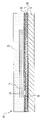
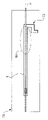
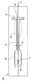
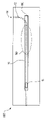
12:導波路
14:入力信号
16:光検出器層
16A:光検出器ダイオード
18:シード窓
20:絶縁体
22:半導体基部
24:埋込酸化物層
26:絶縁体層
28:部分
30、402、402’、502、602、702:光検出器層延長部
404、406、406’、506:光検出器層延長部部分
32、36:光検出器ダイオードの部分
34、38:金属コンタクト
Claims (25)
- 基板上に延び、導波路材料を含む導波路と、
前記導波路上に形成され、光信号の入射部から離れたところに前記導波路を露出する開口部を有する絶縁層と、
前記絶縁層上に形成されるとともに前記導波路と接触するように前記開口部内に形成された光検出器層であって、前記開口部における第1の端部と前記開口部から遠位の第2の端部とを有し、前記導波路材料とゲルマニウムとの傾斜材料であり、前記傾斜材料の導波路材料部分が前記第1の端部における最大から前記第2の端部における最小まで変化し、前記傾斜材料のゲルマニウム部分が前記第1の端部における最小から前記第2の端部における最大まで変化する、光検出器層と、
前記第2の端部における光検出器領域と、
前記第2の端部における前記光検出器層から角度を成して延び、前記光検出器領域に形成される欠陥の欠陥ゲッタ領域である光検出器層延長部と、
を含む、光検出器。 - 前記光検出器層延長部が、前記光検出器領域のいずれの部分も含まない、請求項1に記載の光検出器。
- 前記光検出器層延長部がL形である、請求項1又は2に記載の光検出器。
- 前記光検出器層延長部が湾曲している、請求項1又は2に記載の光検出器。
- 前記光検出器層及び前記光検出器層延長部が共面である、請求項1から4のいずれか一項に記載の光検出器。
- 前記導波路材料がシリコンを含む、請求項1から5のいずれか一項に記載の光検出器。
- 前記光検出器層が前記第1の端部において、前記第2の端部の前記光検出器層の幅より広い幅を有する、請求項1から6のいずれか一項に記載の光検出器。
- 前記光検出器層延長部が、前記光検出器層から一方向にのみ角度を成して延びる、請求項1から7のいずれか一項に記載の光検出器。
- 基板上に延び、シリコンを含む導波路と、
前記導波路上に形成され、光信号の入射部から離れたところに前記導波路を露出する開口部を有する絶縁層と、
前記絶縁層上に形成されるとともに前記導波路と接触するように前記開口部内に形成される線形光検出器層であって、前記開口部における第1の端部と前記線形光検出器層の末端における第2の端部とを有し、前記シリコンとゲルマニウムとの傾斜材料であり、前記傾斜材料のシリコン部分が前記第1の端部における最大から前記第2の端部における最小まで変化し、前記傾斜材料のゲルマニウム部分が前記第1の端部における最小から前記第2の端部における最大まで変化する、線形光検出器層と、
前記線形光検出器層の前記末端における光検出器と、
前記線形光検出器層の前記末端から角度を成して延び、前記光検出器に形成される欠陥の欠陥ゲッタ領域である光検出器層延長部と、
を含む、光検出器。 - 前記光検出器層延長部が、前記線形光検出器層から一方向にのみ角度を成して延びる、請求項9に記載の光検出器。
- 前記光検出器層延長部が、前記線形光検出器層から二方向に角度を成して延びる、請求項9に記載の光検出器。
- 前記光検出器層延長部が、前記線形光検出器層と平行かつ離間した部分を含む、請求項9から11のいずれか一項に記載の光検出器。
- 前記光検出器層延長部が湾曲している、請求項9から12のいずれか一項に記載の光検出器。
- 前記光検出器層及び前記光検出器層延長部が共面である、請求項9から13のいずれか一項に記載の光検出器。
- 前記光検出器層が前記第1の端部において、前記第2の端部の前記光検出器層の幅より広い幅を有する、請求項9から14のいずれか一項に記載の光検出器。
- 基板上に延び、シリコンを含む導波路と、
前記導波路上に形成され、光信号の入射部から離れたところに前記導波路を露出する開口部を有する絶縁層と、
前記絶縁層上に形成されるとともに前記導波路と接触するように前記開口部内に形成される光検出器層であって、前記開口部における第1の端部と、前記光検出器層内に形成された光検出器領域における第2の端部とを有し、前記シリコンとゲルマニウムとの傾斜材料であり、前記傾斜材料のシリコン部分が前記第1の端部における最大から前記第2の端部における最小まで変化し、前記傾斜材料のゲルマニウム部分が前記第1の端部における最小から前記第2の端部における最大まで変化する、光検出器層と、
前記光検出器層と共面になるように、前記光検出器層の前記第2の端部から角度を成して延び、前記光検出器領域に形成される欠陥の欠陥ゲッタ領域である光検出器層延長部と、
を含む、光検出器。 - 前記光検出器層延長部が、前記光検出器領域のいずれの部分も含まない、請求項16に記載の光検出器。
- 前記光検出器層延長部が、前記光検出器層から一方向にのみ角度を成して延びる、請求項16又は17に記載の光検出器。
- 前記光検出器層延長部が、前記光検出器層から二方向に角度を成して延びる、請求項16から17のいずれか一項に記載の光検出器。
- 前記光検出器層延長部が、前記光検出器層と平行かつ離間した部分を含む、請求項16から18のいずれか一項に記載の光検出器。
- 前記光検出器層が前記第1の端部において、前記第2の端部の前記光検出器層の幅より広い幅を有する、請求項16から20のいずれか一項に記載の光検出器。
- 基板上に延び、主部分に接合する入力部分を有し、前記入力部分が前記主部分に対して角度を成している、導波路と、
前記導波路上に形成され、光信号の入射部から離れたところに前記導波路の前記主部分を露出する開口部を有する絶縁層と、
前記絶縁層上に形成されるとともに前記導波路の前記主部分と接触するように前記開口部内に形成される光検出器層であって、前記開口部における第1の端部と、前記第1の端部から離間した第2の端部とを有し、シリコンとゲルマニウムとの傾斜材料であり、前記傾斜材料のシリコン部分が前記第1の端部における最大から前記第2の端部における最小まで変化し、前記傾斜材料のゲルマニウム部分が前記第1の端部における最小から前記第2の端部における最大まで変化する、光検出器層と、
を含み、
前記導波路の前記主部分は、前記導波路の前記主部分が前記導波路の前記入力部分と接合するところから前記光検出器層の下を前記開口部を通り越して延び、前記入力部分は、前記光検出器層の下から外方に突き出し、前記光検出器層の延長部部分は、前記導波路の前記主部分が前記導波路の入力部分と接合するところを通り越して前記第2の端部まで延びており、
前記導波路の前記入力部分が前記導波路の前記主部分と接合するところから始まって前記第1の端部に向かって延びる、前記光検出器層内に形成された光検出器領域をさらに含み、
前記延長部部分が前記接合するところを通り越して前記第2の端部まで延びる距離が、前記光検出器領域に形成される欠陥が最小限になるように決定され、前記欠陥が前記延長部部分に存在して前記光検出器領域には存在しない、
光検出器。 - 前記光検出器層の前記延長部部分が、前記光検出器領域のいずれの部分も含まない、請求項22に記載の光検出器。
- 基板上に延び、主部分に接合する入力部分を有し、前記入力部分が前記主部分に対して角度を成している、シリコン導波路と、
前記導波路上に形成され、光信号の入射部から離れたところにシリコンシードを露出する開口部を有する絶縁層と、
前記絶縁層上に形成されるとともに前記シリコンシードと接触するように前記開口部内に形成される光検出器層であって、前記開口部における第1の端部と、前記第1の端部から離間した第2の端部とを有し、前記シリコンとゲルマニウムとの傾斜材料であり、前記傾斜材料のシリコン部分が前記第1の端部における最大から前記第2の端部における最小まで変化し、前記傾斜材料のゲルマニウム部分が前記第1の端部における最小から前記第2の端部における最大まで変化する、光検出器層と、
を含み、
前記導波路の前記主部分は、前記導波路の前記主部分が前記導波路の前記入力部分と接合するところから前記光検出器層の下を前記第2の端部を通り越して延び、前記入力部分は、前記光検出器層の下から外方に突き出し、前記光検出器層の一部分は、前記導波路の前記主部分が前記導波路の入力部分と接合するところを通り越して前記第1の端部まで延びており、
前記第2の端部よりも手前において、前記導波路の前記主部分の上に、前記光検出器層内に形成された光検出器領域であって、欠陥が前記第2の端部に存在して当該光検出器領域には存在しない光検出器領域をさらに含む、
光検出器。 - 前記シリコンシードが前記導波路から切り離されている、請求項24に記載の光検出器。
Applications Claiming Priority (3)
| Application Number | Priority Date | Filing Date | Title |
|---|---|---|---|
| US15/486,810 US10103280B1 (en) | 2017-04-13 | 2017-04-13 | Rapid melt growth photodetector |
| US15/486,810 | 2017-04-13 | ||
| PCT/IB2018/052487 WO2018189666A1 (en) | 2017-04-13 | 2018-04-10 | Rapid melt growth photodetector |
Publications (2)
| Publication Number | Publication Date |
|---|---|
| JP2020513155A JP2020513155A (ja) | 2020-04-30 |
| JP7128200B2 true JP7128200B2 (ja) | 2022-08-30 |
Family
ID=63761684
Family Applications (1)
| Application Number | Title | Priority Date | Filing Date |
|---|---|---|---|
| JP2019552454A Active JP7128200B2 (ja) | 2017-04-13 | 2018-04-10 | 急速溶融成長光検出器 |
Country Status (6)
| Country | Link |
|---|---|
| US (1) | US10103280B1 (ja) |
| JP (1) | JP7128200B2 (ja) |
| CN (1) | CN110462848B (ja) |
| DE (1) | DE112018000637B4 (ja) |
| GB (1) | GB2575750B (ja) |
| WO (1) | WO2018189666A1 (ja) |
Families Citing this family (2)
| Publication number | Priority date | Publication date | Assignee | Title |
|---|---|---|---|---|
| US11588062B2 (en) * | 2020-10-08 | 2023-02-21 | Globalfoundries U.S. Inc. | Photodetectors including a coupling region with multiple tapers |
| US11609377B2 (en) | 2021-05-03 | 2023-03-21 | Globalfoundries U.S. Inc. | Photodetectors and terminators having a curved shape |
Citations (2)
| Publication number | Priority date | Publication date | Assignee | Title |
|---|---|---|---|---|
| JP2013529854A (ja) | 2010-07-02 | 2013-07-22 | インターナショナル・ビジネス・マシーンズ・コーポレーション | 光検出デバイス及びその形成方法 |
| US20170062647A1 (en) | 2015-08-27 | 2017-03-02 | Globalfoundries Inc. | Photodetector methods and photodetector structures |
Family Cites Families (14)
| Publication number | Priority date | Publication date | Assignee | Title |
|---|---|---|---|---|
| JP4267266B2 (ja) | 2001-07-10 | 2009-05-27 | 株式会社半導体エネルギー研究所 | 半導体装置の作製方法 |
| US7122392B2 (en) | 2003-06-30 | 2006-10-17 | Intel Corporation | Methods of forming a high germanium concentration silicon germanium alloy by epitaxial lateral overgrowth and structures formed thereby |
| US7603016B1 (en) * | 2007-04-30 | 2009-10-13 | The United States Of America As Represented By The Secretary Of The Air Force | Semiconductor photonic nano communication link apparatus |
| US8343792B2 (en) | 2007-10-25 | 2013-01-01 | Bae Systems Information And Electronic Systems Integration Inc. | Method for manufacturing lateral germanium detectors |
| US7902620B2 (en) | 2008-08-14 | 2011-03-08 | International Business Machines Corporation | Suspended germanium photodetector for silicon waveguide |
| JP5812002B2 (ja) * | 2010-07-16 | 2015-11-11 | 日本電気株式会社 | 受光素子及びそれを備えた光通信デバイス、並びに受光素子の製造方法及び光通信デバイスの製造方法 |
| US8633067B2 (en) * | 2010-11-22 | 2014-01-21 | International Business Machines Corporation | Fabricating photonics devices fully integrated into a CMOS manufacturing process |
| WO2012083862A1 (en) * | 2010-12-22 | 2012-06-28 | Bing Li | Waveguide photodetector and forming method thereof |
| US9229164B2 (en) * | 2013-04-23 | 2016-01-05 | Globalfoundries Inc. | Butt-coupled buried waveguide photodetector |
| WO2015016942A1 (en) | 2013-08-02 | 2015-02-05 | Intel Corporation | Low voltage photodetectors |
| US9171971B2 (en) | 2013-10-31 | 2015-10-27 | Globalfoundries U.S. 2 Llc | Encapsulated sensors |
| GB2526880A (en) * | 2014-06-06 | 2015-12-09 | Univ Southampton | Melt-growth of single-crystal alloy semiconductor structures and semiconductor assemblies incorporating such structures |
| US9627575B2 (en) * | 2014-09-11 | 2017-04-18 | International Business Machines Corporation | Photodiode structures |
| CN205723580U (zh) * | 2016-05-09 | 2016-11-23 | 厦门市计量检定测试院 | Si基Ge混合型波导光电探测器 |
-
2017
- 2017-04-13 US US15/486,810 patent/US10103280B1/en active Active
-
2018
- 2018-04-10 GB GB1915262.8A patent/GB2575750B/en active Active
- 2018-04-10 DE DE112018000637.9T patent/DE112018000637B4/de active Active
- 2018-04-10 CN CN201880023166.1A patent/CN110462848B/zh active Active
- 2018-04-10 JP JP2019552454A patent/JP7128200B2/ja active Active
- 2018-04-10 WO PCT/IB2018/052487 patent/WO2018189666A1/en not_active Ceased
Patent Citations (2)
| Publication number | Priority date | Publication date | Assignee | Title |
|---|---|---|---|---|
| JP2013529854A (ja) | 2010-07-02 | 2013-07-22 | インターナショナル・ビジネス・マシーンズ・コーポレーション | 光検出デバイス及びその形成方法 |
| US20170062647A1 (en) | 2015-08-27 | 2017-03-02 | Globalfoundries Inc. | Photodetector methods and photodetector structures |
Non-Patent Citations (1)
| Title |
|---|
| LITTLEJOHNS, C. G. et al.,Towards a fully functional integrated photonic-electronic platform via a single SiGe growth step, SCIENTIFIC REPORTS,2016年01月19日,Vol.6,pp. 19425-1 - 19425-6 |
Also Published As
| Publication number | Publication date |
|---|---|
| JP2020513155A (ja) | 2020-04-30 |
| CN110462848B (zh) | 2023-02-28 |
| US10103280B1 (en) | 2018-10-16 |
| US20180301568A1 (en) | 2018-10-18 |
| WO2018189666A1 (en) | 2018-10-18 |
| DE112018000637B4 (de) | 2024-09-12 |
| DE112018000637T5 (de) | 2019-11-14 |
| GB2575750A (en) | 2020-01-22 |
| CN110462848A (zh) | 2019-11-15 |
| GB201915262D0 (en) | 2019-12-04 |
| GB2575750B (en) | 2020-07-15 |
Similar Documents
| Publication | Publication Date | Title |
|---|---|---|
| US7122392B2 (en) | Methods of forming a high germanium concentration silicon germanium alloy by epitaxial lateral overgrowth and structures formed thereby | |
| US9178085B2 (en) | Waveguide photodetector and forming method thereof | |
| CN105378937B (zh) | 低电压光电检测器 | |
| JP6785057B2 (ja) | 半導体装置およびその製造方法 | |
| US9425341B2 (en) | P-I-N photodiode with dopant diffusion barrier layer | |
| EP3306679B1 (en) | Light-receiving element and optical integrated circuit | |
| US20070104441A1 (en) | Laterally-integrated waveguide photodetector apparatus and related coupling methods | |
| WO2011101632A1 (en) | Electro-optic device | |
| CN102782880B (zh) | 具有改进响应度的基于硅的肖特基势垒探测器 | |
| JP2015046429A (ja) | 受光素子およびその製造方法 | |
| JP7128200B2 (ja) | 急速溶融成長光検出器 | |
| US11164986B2 (en) | Avalanche photodiode and method of manufacturing the same | |
| KR20120069127A (ko) | 아발란치 포토다이오드의 제조방법 | |
| JP4861388B2 (ja) | アバランシェホトダイオード | |
| JP2006506819A (ja) | 発光半導体素子と発光半導体素子の製造方法 | |
| US9076921B2 (en) | Dark current reduction for large area photodiodes | |
| JP6228874B2 (ja) | 半導体光素子 | |
| JP6228873B2 (ja) | 半導体光素子の製造方法 | |
| US11227958B2 (en) | Circular grating structure for photonic device | |
| US12009450B2 (en) | Optical receiving element and manufacturing method therefor | |
| CN210325799U (zh) | 一种光集成器件结构 | |
| JPS6180875A (ja) | 半導体装置 | |
| Tseng et al. | Graded Ge 1− x Sn x photodetectors fabricated on Si substrates by rapid melt growth method | |
| JPS616876A (ja) | 半導体装置 | |
| JPS59103385A (ja) | 半導体装置 |
Legal Events
| Date | Code | Title | Description |
|---|---|---|---|
| A521 | Request for written amendment filed |
Free format text: JAPANESE INTERMEDIATE CODE: A523 Effective date: 20200305 |
|
| A621 | Written request for application examination |
Free format text: JAPANESE INTERMEDIATE CODE: A621 Effective date: 20200909 |
|
| A977 | Report on retrieval |
Free format text: JAPANESE INTERMEDIATE CODE: A971007 Effective date: 20210623 |
|
| A131 | Notification of reasons for refusal |
Free format text: JAPANESE INTERMEDIATE CODE: A131 Effective date: 20210706 |
|
| A521 | Request for written amendment filed |
Free format text: JAPANESE INTERMEDIATE CODE: A523 Effective date: 20210928 |
|
| A131 | Notification of reasons for refusal |
Free format text: JAPANESE INTERMEDIATE CODE: A131 Effective date: 20220208 |
|
| A601 | Written request for extension of time |
Free format text: JAPANESE INTERMEDIATE CODE: A601 Effective date: 20220304 |
|
| RD04 | Notification of resignation of power of attorney |
Free format text: JAPANESE INTERMEDIATE CODE: A7424 Effective date: 20220502 |
|
| A521 | Request for written amendment filed |
Free format text: JAPANESE INTERMEDIATE CODE: A523 Effective date: 20220705 |
|
| TRDD | Decision of grant or rejection written | ||
| A01 | Written decision to grant a patent or to grant a registration (utility model) |
Free format text: JAPANESE INTERMEDIATE CODE: A01 Effective date: 20220809 |
|
| A61 | First payment of annual fees (during grant procedure) |
Free format text: JAPANESE INTERMEDIATE CODE: A61 Effective date: 20220818 |
|
| R150 | Certificate of patent or registration of utility model |
Ref document number: 7128200 Country of ref document: JP Free format text: JAPANESE INTERMEDIATE CODE: R150 |