JP7128200B2 - Rapid melt growth photodetector - Google Patents
Rapid melt growth photodetector Download PDFInfo
- Publication number
- JP7128200B2 JP7128200B2 JP2019552454A JP2019552454A JP7128200B2 JP 7128200 B2 JP7128200 B2 JP 7128200B2 JP 2019552454 A JP2019552454 A JP 2019552454A JP 2019552454 A JP2019552454 A JP 2019552454A JP 7128200 B2 JP7128200 B2 JP 7128200B2
- Authority
- JP
- Japan
- Prior art keywords
- photodetector
- layer
- waveguide
- photodetector layer
- germanium
- Prior art date
- Legal status (The legal status is an assumption and is not a legal conclusion. Google has not performed a legal analysis and makes no representation as to the accuracy of the status listed.)
- Active
Links
- 229910052732 germanium Inorganic materials 0.000 claims description 129
- GNPVGFCGXDBREM-UHFFFAOYSA-N germanium atom Chemical compound [Ge] GNPVGFCGXDBREM-UHFFFAOYSA-N 0.000 claims description 129
- 239000000463 material Substances 0.000 claims description 55
- XUIMIQQOPSSXEZ-UHFFFAOYSA-N Silicon Chemical compound [Si] XUIMIQQOPSSXEZ-UHFFFAOYSA-N 0.000 claims description 54
- 229910052710 silicon Inorganic materials 0.000 claims description 54
- 239000010703 silicon Substances 0.000 claims description 54
- 230000007547 defect Effects 0.000 claims description 27
- 239000000758 substrate Substances 0.000 claims description 16
- 230000003287 optical effect Effects 0.000 claims description 15
- 238000000034 method Methods 0.000 description 19
- 230000008901 benefit Effects 0.000 description 15
- 239000012212 insulator Substances 0.000 description 14
- 230000008569 process Effects 0.000 description 11
- 239000002184 metal Substances 0.000 description 6
- 238000001953 recrystallisation Methods 0.000 description 6
- 230000015572 biosynthetic process Effects 0.000 description 4
- 239000013078 crystal Substances 0.000 description 4
- 150000004767 nitrides Chemical class 0.000 description 3
- 239000004065 semiconductor Substances 0.000 description 3
- 239000002800 charge carrier Substances 0.000 description 2
- 238000000151 deposition Methods 0.000 description 2
- 238000002844 melting Methods 0.000 description 2
- 230000008018 melting Effects 0.000 description 2
- 238000012986 modification Methods 0.000 description 2
- 230000004048 modification Effects 0.000 description 2
- 241000473391 Archosargus rhomboidalis Species 0.000 description 1
- 240000007594 Oryza sativa Species 0.000 description 1
- 235000007164 Oryza sativa Nutrition 0.000 description 1
- 229910000577 Silicon-germanium Inorganic materials 0.000 description 1
- LEVVHYCKPQWKOP-UHFFFAOYSA-N [Si].[Ge] Chemical compound [Si].[Ge] LEVVHYCKPQWKOP-UHFFFAOYSA-N 0.000 description 1
- 230000005540 biological transmission Effects 0.000 description 1
- 238000004891 communication Methods 0.000 description 1
- 230000000295 complement effect Effects 0.000 description 1
- 238000011109 contamination Methods 0.000 description 1
- 230000007423 decrease Effects 0.000 description 1
- 238000005516 engineering process Methods 0.000 description 1
- 238000005530 etching Methods 0.000 description 1
- 230000001771 impaired effect Effects 0.000 description 1
- 239000007943 implant Substances 0.000 description 1
- 238000005304 joining Methods 0.000 description 1
- 238000004519 manufacturing process Methods 0.000 description 1
- 229910044991 metal oxide Inorganic materials 0.000 description 1
- 150000004706 metal oxides Chemical class 0.000 description 1
- 230000005693 optoelectronics Effects 0.000 description 1
- 230000008520 organization Effects 0.000 description 1
- 238000000059 patterning Methods 0.000 description 1
- 230000004044 response Effects 0.000 description 1
- 230000004043 responsiveness Effects 0.000 description 1
- 235000009566 rice Nutrition 0.000 description 1
- -1 seed window 18 Chemical compound 0.000 description 1
Images


Classifications
-
- H—ELECTRICITY
- H10—SEMICONDUCTOR DEVICES; ELECTRIC SOLID-STATE DEVICES NOT OTHERWISE PROVIDED FOR
- H10F—INORGANIC SEMICONDUCTOR DEVICES SENSITIVE TO INFRARED RADIATION, LIGHT, ELECTROMAGNETIC RADIATION OF SHORTER WAVELENGTH OR CORPUSCULAR RADIATION
- H10F77/00—Constructional details of devices covered by this subclass
- H10F77/40—Optical elements or arrangements
- H10F77/413—Optical elements or arrangements directly associated or integrated with the devices, e.g. back reflectors
-
- G—PHYSICS
- G02—OPTICS
- G02B—OPTICAL ELEMENTS, SYSTEMS OR APPARATUS
- G02B6/00—Light guides; Structural details of arrangements comprising light guides and other optical elements, e.g. couplings
- G02B6/24—Coupling light guides
- G02B6/42—Coupling light guides with opto-electronic elements
- G02B6/4295—Coupling light guides with opto-electronic elements coupling with semiconductor devices activated by light through the light guide, e.g. thyristors, phototransistors
-
- H—ELECTRICITY
- H10—SEMICONDUCTOR DEVICES; ELECTRIC SOLID-STATE DEVICES NOT OTHERWISE PROVIDED FOR
- H10F—INORGANIC SEMICONDUCTOR DEVICES SENSITIVE TO INFRARED RADIATION, LIGHT, ELECTROMAGNETIC RADIATION OF SHORTER WAVELENGTH OR CORPUSCULAR RADIATION
- H10F30/00—Individual radiation-sensitive semiconductor devices in which radiation controls the flow of current through the devices, e.g. photodetectors
- H10F30/20—Individual radiation-sensitive semiconductor devices in which radiation controls the flow of current through the devices, e.g. photodetectors the devices having potential barriers, e.g. phototransistors
- H10F30/21—Individual radiation-sensitive semiconductor devices in which radiation controls the flow of current through the devices, e.g. photodetectors the devices having potential barriers, e.g. phototransistors the devices being sensitive to infrared, visible or ultraviolet radiation
- H10F30/22—Individual radiation-sensitive semiconductor devices in which radiation controls the flow of current through the devices, e.g. photodetectors the devices having potential barriers, e.g. phototransistors the devices being sensitive to infrared, visible or ultraviolet radiation the devices having only one potential barrier, e.g. photodiodes
-
- H—ELECTRICITY
- H10—SEMICONDUCTOR DEVICES; ELECTRIC SOLID-STATE DEVICES NOT OTHERWISE PROVIDED FOR
- H10F—INORGANIC SEMICONDUCTOR DEVICES SENSITIVE TO INFRARED RADIATION, LIGHT, ELECTROMAGNETIC RADIATION OF SHORTER WAVELENGTH OR CORPUSCULAR RADIATION
- H10F39/00—Integrated devices, or assemblies of multiple devices, comprising at least one element covered by group H10F30/00, e.g. radiation detectors comprising photodiode arrays
- H10F39/10—Integrated devices
- H10F39/12—Image sensors
-
- H—ELECTRICITY
- H10—SEMICONDUCTOR DEVICES; ELECTRIC SOLID-STATE DEVICES NOT OTHERWISE PROVIDED FOR
- H10F—INORGANIC SEMICONDUCTOR DEVICES SENSITIVE TO INFRARED RADIATION, LIGHT, ELECTROMAGNETIC RADIATION OF SHORTER WAVELENGTH OR CORPUSCULAR RADIATION
- H10F71/00—Manufacture or treatment of devices covered by this subclass
-
- H—ELECTRICITY
- H10—SEMICONDUCTOR DEVICES; ELECTRIC SOLID-STATE DEVICES NOT OTHERWISE PROVIDED FOR
- H10F—INORGANIC SEMICONDUCTOR DEVICES SENSITIVE TO INFRARED RADIATION, LIGHT, ELECTROMAGNETIC RADIATION OF SHORTER WAVELENGTH OR CORPUSCULAR RADIATION
- H10F77/00—Constructional details of devices covered by this subclass
- H10F77/10—Semiconductor bodies
- H10F77/14—Shape of semiconductor bodies; Shapes, relative sizes or dispositions of semiconductor regions within semiconductor bodies
- H10F77/148—Shapes of potential barriers
-
- G—PHYSICS
- G02—OPTICS
- G02B—OPTICAL ELEMENTS, SYSTEMS OR APPARATUS
- G02B6/00—Light guides; Structural details of arrangements comprising light guides and other optical elements, e.g. couplings
- G02B6/10—Light guides; Structural details of arrangements comprising light guides and other optical elements, e.g. couplings of the optical waveguide type
- G02B6/12—Light guides; Structural details of arrangements comprising light guides and other optical elements, e.g. couplings of the optical waveguide type of the integrated circuit kind
- G02B2006/12035—Materials
- G02B2006/12061—Silicon
Landscapes
- Physics & Mathematics (AREA)
- General Physics & Mathematics (AREA)
- Optics & Photonics (AREA)
- Light Receiving Elements (AREA)
- Optical Integrated Circuits (AREA)
Description
本例示的実施形態は、光電子デバイスに関し、より具体的には光信号を電気信号に変換する導波路光検出器に関する。 TECHNICAL FIELD The present exemplary embodiments relate to optoelectronic devices, and more particularly to waveguide photodetectors that convert optical signals into electrical signals.
光通信システムにおいて、光導波路は、システムの一方の端にある光源、例えばレーザによって生成された光信号をシステムの他端にある検出器、例えば光検出器に案内するための伝送チャネルを提供する。活性領域である光検出器材料は、伝送された光信号の光子からエネルギーを吸収し、これに応答して、電荷キャリア、例えば電子及び正孔を励起する。逆バイアス電圧を印加すると、励起された電荷キャリアは、光検出器上のコンタクトに引き寄せられ、それにより光信号に対応する電流を発生させる。このようにして、光検出器は、光信号を電気信号に変換する。 In an optical communication system, an optical waveguide provides a transmission channel for guiding an optical signal produced by a light source, e.g. a laser, at one end of the system to a detector, e.g. a photodetector, at the other end of the system. . The active region, the photodetector material, absorbs energy from the photons of the transmitted optical signal and excites charge carriers such as electrons and holes in response. Upon application of a reverse bias voltage, the excited charge carriers are attracted to the contacts on the photodetector, thereby generating a current corresponding to the optical signal. Thus, the photodetector converts the optical signal into an electrical signal.
ゲルマニウムは、シリコン上で成長するその潜在能力ゆえに、光検出器にふさわしい選択肢である。 Germanium is a good choice for photodetectors because of its potential to grow on silicon.
格子定数は、結晶格子内の単位セル間の距離を意味する。ゲルマニウムの格子定数は、シリコンの格子定数と完全に一致しているわけではなく、ゲルマニウムの格子定数はシリコンの格子定数よりわずかに大きい。ゲルマニウムとシリコンの格子定数間の不一致は、結晶を成長させるための通常のエピタキシャル成長(「EPI」)技術の使用に関して課題を提起する。現在、シリコン基板上に単結晶ゲルマニウムフィルムを作製するための2つの主要な方法が大いに研究されている。1つの方法は、バッファ層、及び選択的エピタキシャル成長(「SEG」)後の後処理の使用である。第2の方法は、急速溶融成長(「RMG」)技術の使用である。これら2つの方法の間では、RMGプロセスの方がより良いプロセス適合性を有するが、構築できる構造に制限がある。 Lattice constant refers to the distance between unit cells in a crystal lattice. The lattice constant of germanium does not perfectly match that of silicon, and the lattice constant of germanium is slightly larger than that of silicon. The mismatch between the lattice constants of germanium and silicon poses challenges for using conventional epitaxial growth (“EPI”) techniques to grow crystals. Currently, two main methods for making single crystal germanium films on silicon substrates are being extensively investigated. One method is the use of a buffer layer and a post-treatment after selective epitaxial growth ("SEG"). A second method is the use of rapid melt growth (“RMG”) technology. Between these two methods, the RMG process has better process compatibility, but is limited in the structures that can be built.
RMG技術では、単結晶ゲルマニウムをシリコン上で直接成長させない。むしろ、ポリゲルマニウム又はアモルファスゲルマニウムを、下にあるシリコン層への開口部(「シード窓」)を有する絶縁体上に堆積させる。ポリゲルマニウム又はアモルファスゲルマニウムを取り囲むように窒化物などの絶縁体が堆積される。RMG法は、堆積されたポリゲルマニウム又はアモルファスゲルマニウムを囲む絶縁体によって形成されたマイクロるつぼを必要とし、これは、アニール処理したときにゲルマニウムの溶融及び再結晶を生じさせる。 The RMG technique does not grow single crystal germanium directly on silicon. Rather, polygermanium or amorphous germanium is deposited on an insulator that has openings (“seed windows”) to the underlying silicon layer. An insulator such as nitride is deposited surrounding the polygermanium or amorphous germanium. The RMG method requires a microcrucible formed by an insulator surrounding deposited polygermanium or amorphous germanium, which causes the germanium to melt and recrystallize when annealed.
CMOS適合プロセスシーケンスにおける光学検出器は、RMGゲルマニウム光検出器を用いて安価に達成することができる。RMG光検出器は、シリコン適合性プロセスで構築されているが、幾つかの難題がある。 Optical detectors in CMOS compatible process sequences can be achieved inexpensively using RMG germanium photodetectors. RMG photodetectors are built on silicon-compatible processes, but present several challenges.
1つの難題は、シリコンシード領域がゲルマニウム光検出器を汚染し、その結果、純粋な結晶性ゲルマニウム光検出器ではなくシリコンゲルマニウム検出器がもたらされるということである。この結果、光検出器の応答性を損なうことがある。 One challenge is that the silicon seed region contaminates the germanium photodetector, resulting in a silicon germanium detector rather than a pure crystalline germanium photodetector. As a result, the responsiveness of the photodetector may be impaired.
別の難題は、ゲルマニウム光検出器の溶融及びその後の再結晶が、光検出器の端部付近において光検出器の収率及び応答性に影響を及ぼす欠陥の形成を生じさせることがあることである。 Another challenge is that the melting and subsequent recrystallization of germanium photodetectors can result in the formation of defects near the edges of the photodetector that affect the yield and responsivity of the photodetector. be.
したがって、当該技術分野において上記課題に対処する必要がある。 Therefore, there is a need in the art to address the above issues.
第1の態様から見て、本発明は、基板上に延び、導波路材料を含む導波路と、導波路上に形成され、導波路を露出する開口部を有する絶縁層と、絶縁層上に形成されるとともに導波路と接触するように開口部内に形成された光検出器層であって、開口部における第1の端部と開口部から遠位の第2の端部とを有し、導波路材料とゲルマニウムとの傾斜材料であり、傾斜材料の導波路材料部分が第1の端部における最大から第2の端部における最小まで変化し、傾斜材料のゲルマニウム部分が第1の端部における最小から第2の端部における最大まで変化する、光検出器層と、第2の端部における光検出器領域と、第2の端部における光検出器層から角度を成して延びる光検出器層延長部と、を含む、光検出器を提供する。 Viewed from a first aspect, the invention comprises a waveguide extending over a substrate and comprising a waveguide material; an insulating layer formed over the waveguide and having an opening exposing the waveguide; a photodetector layer formed and formed within the opening in contact with the waveguide, the photodetector layer having a first end at the opening and a second end distal from the opening; A graded material of a waveguide material and germanium, wherein the waveguide material portion of the graded material varies from a maximum at the first end to a minimum at the second end and the germanium portion of the graded material is at the first end. a photodetector layer at the second end, a photodetector area at the second end, and light extending at an angle from the photodetector layer at the second end, varying from a minimum at to a maximum at the second end and a detector layer extension.
さらなる態様から見て、本発明は、基板上に延び、シリコンを含む導波路と、導波路上に形成され、導波路を露出する開口部を有する絶縁層と、絶縁層上に形成されるとともに導波路と接触するように開口部内に形成される線形光検出器層であって、開口部における第1の端部と線形光検出器層の末端における第2の端部とを有し、シリコンとゲルマニウムとの傾斜材料であり、傾斜材料のシリコン部分が第1の端部における最大から第2の端部における最小まで変化し、傾斜材料のゲルマニウム部分が第1の端部における最小から第2の端部における最大まで変化する、線形光検出器層と、線形光検出器層の末端における光検出器と、線形光検出器層の末端から角度を成して延びる光検出器層延長部と、を含む、光検出器を提供する。 Viewed from further aspects, the invention provides a waveguide extending over a substrate and comprising silicon; an insulating layer formed over the waveguide and having an opening exposing the waveguide; A linear photodetector layer formed in the opening in contact with the waveguide, the linear photodetector layer having a first end at the opening and a second end at a distal end of the linear photodetector layer, the silicon and germanium, wherein the silicon portion of the graded material varies from a maximum at the first end to a minimum at the second end, and the germanium portion of the graded material varies from a minimum at the first end to a second a linear photodetector layer, a photodetector at the end of the linear photodetector layer, and a photodetector layer extension extending at an angle from the end of the linear photodetector layer, varying to a maximum at the end of A photodetector is provided, comprising:
さらなる態様から見て、本発明は、基板上に延び、シリコンを含む導波路と、導波路上に形成され、導波路を露出する開口部を有する絶縁層と、絶縁層上に形成されるとともに導波路と接触するように開口部内に形成される光検出器層であって、開口部における第1の端部と、光検出器層内に形成された光検出器領域における第2の端部とを有し、シリコンとゲルマニウムとの傾斜材料であり、傾斜材料のシリコン部分が第1の端部における最大から第2の端部における最小まで変化し、傾斜材料のゲルマニウム部分が第1の端部における最小から第2の端部における最大まで変化する、光検出器層と、光検出器層と共面になるように、光検出器層から角度を成して延びる光検出器層延長部と、を含む、光検出器を提供する。 Viewed from further aspects, the invention provides a waveguide extending over a substrate and comprising silicon; an insulating layer formed over the waveguide and having an opening exposing the waveguide; A photodetector layer formed in the opening in contact with the waveguide, the first end at the opening and the second end at the photodetector region formed in the photodetector layer. and a graded material of silicon and germanium, wherein the silicon portion of the graded material varies from a maximum at the first end to a minimum at the second end, and the germanium portion of the graded material is at the first end. a photodetector layer varying from a minimum at the portion to a maximum at the second end; and a photodetector layer extension extending angularly from the photodetector layer so as to be coplanar with the photodetector layer. and a photodetector.
さらなる態様から見て、本発明は、基板上に延び、主部分に接合する入力部分を有し、入力部分が主部分に対して角度を成している、導波路と、導波路上に形成され、導波路の主部分を露出する開口部を有する絶縁層と、絶縁層上に形成されるとともに導波路の主部分と接触するように開口部内に形成される光検出器層であって、開口部における第1の端部と、第1の端部から離間した第2の端部とを有し、シリコンとゲルマニウムとの傾斜材料であり、傾斜材料のシリコン部分が第1の端部における最大から第2の端部における最小まで変化し、傾斜材料のゲルマニウム部分が第1の端部における最小から第2の端部における最大まで変化する、光検出器層と、を含み、導波路の主部分は、導波路の主部分が導波路の入力部分と接合するところから光検出器層の下を開口部を通り越して延び、入力部分は、光検出器層の下から外方に突き出し、光検出器層の延長部部分は、導波路の主部分が導波路の入力部分と接合するところを通り越して第2の端部まで延びており、導波路の入力部分が導波路の主部分と接合するところから始まって第1の端部に向かって延びる、光検出器層内に形成された光検出器領域をさらに含む、光検出器を提供する。 Viewed from a further aspect, the invention provides a waveguide extending over a substrate and having an input portion joined to a main portion, the input portion being angled with respect to the main portion, and a waveguide formed on the waveguide. an insulating layer having an opening exposing a main portion of the waveguide; and a photodetector layer formed on the insulating layer and in the opening in contact with the main portion of the waveguide, comprising: a graded material of silicon and germanium having a first end at the opening and a second end spaced from the first end, the silicon portion of the graded material being at the first end; a photodetector layer varying from a maximum to a minimum at the second end, wherein the germanium portion of the graded material varies from a minimum at the first end to a maximum at the second end; the main portion extends through the opening under the photodetector layer from where the main portion of the waveguide joins the input portion of the waveguide, the input portion projecting outwardly from below the photodetector layer; The extension portion of the photodetector layer extends to the second end past where the main portion of the waveguide joins the input portion of the waveguide, the input portion of the waveguide joining the main portion of the waveguide. A photodetector is provided further including a photodetector region formed in the photodetector layer beginning at the junction and extending toward the first end.
さらなる態様から見て、本発明は、基板上に延び、主部分に接合する入力部分を有し、入力部分が主部分に対して角度を成している、シリコン導波路と、導波路上に形成され、シリコンシードを露出する開口部を有する絶縁層と、絶縁層上に形成されるとともに導波路のシリコンシードと接触するように開口部内に形成される光検出器層であって、開口部における第1の端部と、第1の端部から離間した第2の端部とを有し、シリコンとゲルマニウムとの傾斜材料であり、傾斜材料のシリコン部分が第1の端部における最大から第2の端部における最小まで変化し、傾斜材料のゲルマニウム部分が第1の端部における最小から第2の端部における最大まで変化する、光検出器層と、を含み、導波路の主部分は、導波路の主部分が導波路の入力部分と接合するところから光検出器層の下を第2の端部を通り越して延び、入力部分は、光検出器層の下から外方に突き出し、光検出器層の一部分は、導波路の主部分が導波路の入力部分と接合するところを通り越して第1の端部まで延びており、第2の端部において、導波路の主部分の上に、光検出器層内に形成された光検出器領域をさらに含む、光検出器を提供する。 Viewed from a further aspect, the invention provides a silicon waveguide extending over a substrate and having an input portion joined to a main portion, the input portion being angled with respect to the main portion; an insulating layer formed with an opening exposing the silicon seed; and a photodetector layer formed on the insulating layer and in the opening in contact with the silicon seed of the waveguide, the opening comprising: and a second end spaced from the first end and a graded material of silicon and germanium, wherein the silicon portion of the graded material extends from a maximum at the first end to a a photodetector layer varying to a minimum at the second end, wherein the germanium portion of the graded material varies from a minimum at the first end to a maximum at the second end; extends past the second end under the photodetector layer from where the main portion of the waveguide joins the input portion of the waveguide, the input portion projecting outwardly from below the photodetector layer. , a portion of the photodetector layer extends past where the main portion of the waveguide joins the input portion of the waveguide to the first end and at the second end, the main portion of the waveguide. Above, a photodetector is provided further comprising a photodetector region formed within a photodetector layer.
上述及び後述の例示的な実施形態の種々の利点及び目的は、例示的な実施形態の態様に従って、基板上に延び、導波路材料を含む導波路と、導波路上に形成され、導波路を露出する開口部を有する絶縁層と、絶縁層上に形成されるとともに導波路と接触するように開口部内に形成された光検出器層であって、開口部における第1の端部と開口部から遠位の第2の端部とを有し、導波路材料とゲルマニウムとの傾斜材料であり、傾斜材料の導波路材料部分が第1の端部における最大から第2の端部における最小まで変化し、傾斜材料のゲルマニウム部分が第1の端部における最小から第2の端部における最大まで変化する、光検出器層と、第2の端部における光検出器領域と、第2の端部における光検出器層延長部から角度を成して延びる光検出器層延長部と、を含む、光検出器を提供することによって達成される。 Various advantages and objects of the exemplary embodiments described above and below are described in accordance with aspects of the exemplary embodiments, including waveguides extending over a substrate and including waveguide material; an insulating layer having an opening exposed; and a photodetector layer formed on the insulating layer and in the opening in contact with the waveguide, the first end at the opening and the opening. and a second end distal to and a graded material of waveguide material and germanium, wherein the waveguide material portion of the graded material extends from a maximum at the first end to a minimum at the second end a photodetector layer that varies and the germanium portion of the graded material varies from a minimum at the first end to a maximum at the second end; a photodetector region at the second end; and a photodetector layer extension extending at an angle from the photodetector layer extension at the portion.
例示的な実施形態の別の態様によれば、基板上に延び、シリコンを含む導波路と、導波路上に形成され、導波路を露出する開口部を有する絶縁層と、絶縁層上に形成されるとともに導波路と接触するように開口部内に形成される線形光検出器層であって、開口部における第1の端部と線形光検出器層の末端における第2の端部とを有し、シリコンとゲルマニウムとの傾斜材料であり、傾斜材料のシリコン部分が第1の端部における最大から第2の端部における最小まで変化し、傾斜材料のゲルマニウム部分が第1の端部における最小から第2の端部における最大まで変化する、線形光検出器層と、線形光検出器層の末端における光検出器と、線形光検出器層の末端から角度を成して延びる光検出器層延長部と、を含む、光検出器が提供される。 According to another aspect of an exemplary embodiment, a waveguide extending over a substrate and comprising silicon; an insulating layer formed over the waveguide and having an opening exposing the waveguide; and formed over the insulating layer a linear photodetector layer formed in the opening so as to be in contact with the waveguide, the linear photodetector layer having a first end at the opening and a second end at a distal end of the linear photodetector layer; and a graded material of silicon and germanium, the silicon portion of the graded material varying from a maximum at the first end to a minimum at the second end, and the germanium portion of the graded material being a minimum at the first end. to a maximum at the second end, a photodetector at the end of the linear photodetector layer, and a photodetector layer extending at an angle from the end of the linear photodetector layer A photodetector is provided, including an extension.
例示的な実施形態のさらなる態様によれば、基板上に延び、シリコンを含む導波路と、導波路上に形成され、導波路を露出する開口部を有する絶縁層と、絶縁層上に形成されるとともに導波路と接触するように開口部内に形成される光検出器層であって、開口部における第1の端部と、光検出器層内に形成された光検出器領域における第2の端部とを有し、シリコンとゲルマニウムとの傾斜材料であり、傾斜材料のシリコン部分が第1の端部における最大から第2の端部における最小まで変化し、傾斜材料のゲルマニウム部分が第1の端部における最小から第2の端部における最大まで変化する、光検出器層と、光検出器層と共面になるように、光検出器層から角度を成して延びる光検出器層延長部と、を含む、光検出器が提供される。 According to further aspects of the exemplary embodiments, a waveguide extending over the substrate and comprising silicon; an insulating layer formed over the waveguide and having an opening exposing the waveguide; a photodetector layer formed in the opening so as to be in contact with the waveguide and having a first end in the opening and a second end in the photodetector region formed in the photodetector layer; and a graded material of silicon and germanium, the silicon portion of the graded material varying from a maximum at the first end to a minimum at the second end, and the germanium portion of the graded material at the first end. and a photodetector layer extending at an angle from the photodetector layer so as to be coplanar with the photodetector layer, varying from a minimum at the end of the photodetector layer to a maximum at the second end of the photodetector layer. A photodetector is provided, including an extension.
例示的な実施形態の別の態様によれば、基板上に延び、主部分に接合する入力部分を有し、入力部分が主部分に対して角度を成している、導波路と、導波路上に形成され、導波路の主部分を露出する開口部を有する絶縁層と、絶縁層上に形成されるとともに導波路の主部分と接触するように開口部内に形成される光検出器層であって、開口部における第1の端部と、第1の端部から離間した第2の端部とを有し、シリコンとゲルマニウムとの傾斜材料であり、傾斜材料のシリコン部分が第1の端部における最大から第2の端部における最小まで変化し、傾斜材料のゲルマニウム部分が第1の端部における最小から第2の端部における最大まで変化する、光検出器層と、を含み、導波路の主部分は、導波路の主部分が導波路の入力部分と接合するところから光検出器層の下を開口部を通り越して延び、入力部分は、光検出器層の下から外方に突き出し、光検出器層の延長部部分は、導波路の主部分が導波路の入力部分と接合するところを通り越して第2の端部まで延びており、導波路の入力部分が導波路の主部分と接合するところから始まって第1の端部に向かって延びる、光検出器層内に形成された光検出器領域をさらに含む、光検出器が提供される。 According to another aspect of an exemplary embodiment, a waveguide extending over the substrate and having an input portion joined to the main portion, the input portion being angled with respect to the main portion; an insulating layer formed over the waveguide and having an opening exposing a main portion of the waveguide; and a photodetector layer formed over the insulating layer and in the opening so as to contact the main portion of the waveguide. having a first end at the opening and a second end spaced from the first end and being a graded material of silicon and germanium, the silicon portion of the graded material being at the first end; a photodetector layer that varies from a maximum at the end to a minimum at the second end, the germanium portion of the graded material varying from a minimum at the first end to a maximum at the second end; A main portion of the waveguide extends through the opening under the photodetector layer from where the main portion of the waveguide joins the input portion of the waveguide, and the input portion extends outwardly from below the photodetector layer. and the extended portion of the photodetector layer extends past where the main portion of the waveguide joins the input portion of the waveguide to the second end, the input portion of the waveguide A photodetector is provided further including a photodetector region formed in the photodetector layer beginning at the junction with the main portion and extending toward the first end.
例示的な実施形態のさらに別の態様によれば、基板上に延び、主部分に接合する入力部分を有し、入力部分が主部分に対して角度を成している、シリコン導波路と、導波路上に形成され、シリコンシードを露出する開口部を有する絶縁層と、絶縁層上に形成されるとともに導波路のシリコンシードと接触するように開口部内に形成される光検出器層であって、開口部における第1の端部と、第1の端部から離間した第2の端部とを有し、シリコンとゲルマニウムとの傾斜材料であり、傾斜材料のシリコン部分が第1の端部における最大から第2の端部における最小まで変化し、傾斜材料のゲルマニウム部分が第1の端部における最小から第2の端部における最大まで変化する、光検出器層と、を含み、導波路の主部分は、導波路の主部分が導波路の入力部分と接合するところから光検出器層の下を第2の端部を通り越して延び、入力部分は、光検出器層の下から外方に突き出し、光検出器層の一部分は、導波路の主部分が導波路の入力部分と接合するところを通り越して第1の端部まで延びており、第2の端部において、導波路の主部分の上に、光検出器層内に形成された光検出器領域をさらに含む、光検出器が提供される。 According to still further aspects of the exemplary embodiments, a silicon waveguide extending over the substrate and having an input portion joined to the main portion, the input portion being angled with respect to the main portion; an insulating layer formed over the waveguide and having an opening exposing the silicon seed; and a photodetector layer formed over the insulating layer and within the opening so as to contact the silicon seed of the waveguide. has a first end at the opening and a second end spaced from the first end, and is a graded material of silicon and germanium, the silicon portion of the graded material being at the first end. a photodetector layer varying from a maximum at the first end to a minimum at the second end, the germanium portion of the graded material varying from a minimum at the first end to a maximum at the second end; A main portion of the waveguide extends from below the photodetector layer past the second end from where the main portion of the waveguide joins the input portion of the waveguide, and the input portion extends from below the photodetector layer. A portion of the outwardly projecting photodetector layer extends past where the main portion of the waveguide joins the input portion of the waveguide to the first end, and at the second end, the waveguide A photodetector is provided further comprising a photodetector region formed in a photodetector layer over the main portion of the photodetector.
例示的な実施形態の特徴は新規であると考えられ、例示的な実施形態に特徴的な要素は、添付の特許請求の範囲に具体的に述べられている。図面は例示のみを目的としたものであり、縮尺通りに描かれていない。例示的な実施形態は、構成及び動作方法の両方において、添付の図面との組み合わせで解釈される以下の詳細な説明を参照することによって最もよく理解することができる。 The features of the exemplary embodiments are believed to be novel and the elements characteristic of the exemplary embodiments are pointed out with particularity in the appended claims. The drawings are for illustrative purposes only and are not drawn to scale. The illustrative embodiments, both as to organization and method of operation, may best be understood by reference to the following detailed description taken in conjunction with the accompanying drawings.
例示的な実施形態にはいくつかの利点がある。1つの利点は、入射光から離れたところにシリコン・リッチ領域がある光検出器の作成である。別の利点は、光信号の入射部に近いゲルマニウム・リッチ領域である。さらなる利点は、光信号の経路外にある欠陥ゲッタ領域である。 Exemplary embodiments have several advantages. One advantage is the creation of a photodetector with a silicon-rich region remote from the incident light. Another advantage is the germanium-rich region close to the entrance of the optical signal. A further advantage is the defect getter region that is out of the path of the optical signal.
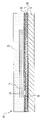
図面をより詳細に参照し、特に図1を参照すると、ゲルマニウム光検出器10の実施形態の平面図である。ゲルマニウム光検出器10は、通常はシリコンである導波路12を含み、矢印14で示される入力信号は、右側からゲルマニウム光検出器10に入ってくる。光検出器層16は、シード窓18を通して、下にある導波路12と接触する。破線の楕円16Aで示される光検出器層16の右側は、光検出器ダイオードを含む。窒化物などの絶縁体20が光検出器層16を囲む。ゲルマニウム光検出器10を囲むのは酸化物(図示せず)であってもよい。
Referring in more detail to the drawings, and in particular to FIG. 1, a plan view of an embodiment of
ゲルマニウム光検出器10(又は後述の実施形態のいずれか)の形成は、CMOS(相補型金属酸化膜半導体)製造ラインにおいて行うことができる。CMOSプロセスによって形成される例示的な実施形態は、ゲルマニウムの汚染及び欠陥の形成に関する従来技術の難題を最小限にすることが見いだされた。 Formation of the germanium photodetector 10 (or any of the embodiments described below) can be done in a CMOS (Complementary Metal Oxide Semiconductor) manufacturing line. Exemplary embodiments formed by CMOS processes have been found to minimize the challenges of the prior art with respect to germanium contamination and defect formation.
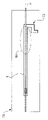
ここで図2を参照すると、図1の矢印2-2の方向で見たゲルマニウム光検出器10の断面図である。ゲルマニウム光検出器10は、シリコンなどの半導体基部22と、それに続く、埋込酸化物層24、導波路12、窒化物などの絶縁体層26、光検出器層16、及び絶縁体20の上に形成することができる。光検出器層16は、シード窓18を通って延びて導波路12に接触する部分28を有する。
Referring now to FIG. 2, which is a cross-sectional view of
ゲルマニウム光検出器10は、埋込酸化物層24上に導波路12を形成し、次いで絶縁体26を形成することを含むプロセスによって形成することができる。絶縁体26内にシード窓18を形成することができる。その後、ポリゲルマニウム又はアモルファスゲルマニウムを、シード窓18を含めて堆積し、次いでパターン付けすることにより、光検出器層16を形成することができる。限定ではなく例示の目的で、光検出器層16は、1μmから5μmの範囲、例えば2.5μm幅の、図1に示されるような幅40を有することができる。ゲルマニウム光検出器層16を絶縁体20によって封入し、次いでRMGプロセスに従って少なくともゲルマニウムの融点まで加熱することができる。
RMGプロセスの結果として、シリコンとゲルマニウムの傾斜が形成される。シリコンのモル分率は、シード窓18において最高であり、徐々に減少して、光検出器ダイオード16Aにおいてゼロ又はゼロ近くになる。逆に、ゲルマニウムのモル分率は、シード窓において最低であり、徐々に増大して、光検出器ダイオード16Aにおいて100%又は100%近くになる。好ましくは、光検出器ダイオード16Aの左の縁部16Bにおけるゲルマニウムのモル分率は、少なくとも95%になるべきである。
As a result of the RMG process, a grade of silicon and germanium is formed. The silicon mole fraction is highest at the
光検出器層16は、1つ又は複数の光検出器層延長部30をさらに含む。限定ではなく例示の目的で、光検出器層延長部は、1μmから10μm、例えば3μmの長さの、図1で示される長さ42を有することができる。光検出器延長部30の利点は、通常は光検出器層16の端部16Cで形成されることがある欠陥が、ここでは光検出器層延長部30内へ押しやられることである。したがって、光検出器ダイオード16A内の光検出器層16がここでは欠陥を有さないので、光検出器ダイオード16Aの収率及び応答性が改善される。
ここで図3を参照すると、図1の矩形21内の光検出器ダイオード16Aがより詳細に示されている。光検出器ダイオード16Aの1つの部分32は、nドープすることができ金属コンタクト34が形成され、他方、第2の部分36は、pドープすることができ、金属コンタクト38が形成される。RMGプロセス後、光検出器ダイオード16Aのドーピングのために絶縁体20を随意に除去して、ドーピング注入エネルギーを最小化することができる。絶縁体20をそのまま残す場合、金属コンタクト34は、絶縁体20を通して局所的にエッチングし、次いで金属コンタクト34のための金属を堆積することによって形成することができる。
Referring now to FIG. 3,
光検出器層16の側部から角度を成して離れた光検出器層延長部30も、より詳細に示されている。光検出器層延長部30は、光検出器層16に対して垂直なものとして示されているが、それより小さい又は大きい角度の延長部を形成することもできる。破線は、光検出器層16が終わり、光検出器層延長部30が始まるところを示している。
ここで図4を参照すると、ゲルマニウム光検出器400の別の例示的な実施形態が示されており、これは、ゲルマニウム光検出器400が、異なる光検出器層延長部402を有すること以外は、ゲルマニウム光検出器10と同様である。光検出器層延長部402は、光検出器層16の側部から角度を成して離れた光検出器層延長部部分404と、光検出器層延長部部分404の側部から角度を成して離れた光検出器層延長部部分406とを含む。1つの実施形態において、光検出器層延長部部分406は、光検出器層16と平行にすることができる。
Referring now to FIG. 4, another exemplary embodiment of a
ここで図5を参照すると、ゲルマニウム光検出器400が改変されて、ここではゲルマニウム光検出器400’となっており、光検出器層延長部部分406は、ここでは長さを増大して光検出器層延長部部分406’として示されている。
Referring now to FIG. 5, the
ゲルマニウム光検出器400、400’の利点は、ゲルマニウムの再結晶中のいかなる欠陥も、ゲルマニウム光検出器層16の端部16Cをさらに越えて光検出器層延長部402内へ押しやられることである。
An advantage of the
ここで図6を参照すると、ゲルマニウム光検出器500の別の例示的な実施形態が示されており、これは、ゲルマニウム光検出器500が、異なる光検出器層延長部502を有すること以外は、ゲルマニウム光検出器10と同様である。光検出器層延長部502は、光検出器層16の側部から角度を成して離れた光検出器層延長部部分504と、光検出器層延長部部分504の側部から角度を成して離れた光検出器層延長部部分506とを含む。1つの実施形態において、光検出器層延長部部分506は、光検出器層16と平行にすることができる。ゲルマニウム光検出器500は、光検出器層延長部部分506の側部から角度を成して離れたものとすることができる付加的な光検出器層延長部508を含むことができる。
Referring now to FIG. 6, another exemplary embodiment of a
ゲルマニウム光検出器500の利点は、ゲルマニウムの再結晶中のいかなる欠陥も、ゲルマニウム光検出器層16の端部16Cをさらに越えて光検出器層延長部502内へ押しやられることである。
An advantage of
ここで図7を参照すると、ゲルマニウム光検出器600の別の例示的な実施形態が示されており、これは、ゲルマニウム光検出器600が、異なる光検出器層延長部602を有すること以外は、ゲルマニウム光検出器10と同様である。光検出器層延長部602は、光検出器層16の一方の側部から湾曲して離れている。限定ではなく例示の目的で、光検出器層延長部602は、1μmから10μm、例えば5μmだけ、一方の側44に偏向することができる。
Referring now to FIG. 7, another exemplary embodiment of a
ゲルマニウム光検出器600の利点は、ゲルマニウムの再結晶中のいかなる欠陥も、ゲルマニウム光検出器層16の端部16Cをさらに越えて光検出器層延長部602内へ押しやられることである。
An advantage of
前述のゲルマニウム光検出器10、400、400’、500はすべて、光検出器層16の両側から角度を成して離れた光検出器層延長部30、402、402’、502を有していた。光検出器層延長部30、402、402’、502が、ゲルマニウム光検出器600の光検出器層延長部602の場合のように片側のみから角度を成して離れることは、例示的な実施形態の範囲内である。図8のゲルマニウム光検出器700は、そうした例の1つであり、光検出器層延長部702は、延長部502が光検出器層16の両側から角度を成して離れたゲルマニウム光検出器500と比べて、光検出器層16の片側のみから角度を成して離れている。
The
ここで図9を参照すると、ゲルマニウム光検出器800の別の例示的な実施形態が示されており、これは、ゲルマニウム光検出器800が、シード窓18の近くに光検出器層16の幅広部分16Dを有すること以外は、ゲルマニウム光検出器10と同様である。限定ではなく例示の目的で、光検出器層16は、0.5μmから3μmの範囲、例えば1.0μm幅の、図9に示されるような幅40を有することができる。さらに、限定ではなく例示の目的で、幅広部分16Dは、光検出器層16の幅40の1.5倍から5倍、例えば3倍の、図9に示されるような最大幅46を有することができる。幅広部分16Dは、シード窓18から幅広部分16Dが光検出器層16と交わるところまで徐々に先細になっていることに留意されたい。
Referring now to FIG. 9, there is shown another exemplary embodiment of a
ゲルマニウム光検出器800の利点は、ゲルマニウムの再結晶中のいかなる欠陥も、ゲルマニウム光検出器層16の端部16Cをさらに越えて光検出器層延長部30内へ押しやられることである。ゲルマニウム光検出器800の別の利点は、光検出器層16の幅広部分16Dが光検出器ダイオード16A内のゲルマニウムのモル分率の増大を助けることである。
An advantage of
ここで図10を参照すると、ゲルマニウム光検出器900の別の例示的な実施形態が示されており、これは、ゲルマニウム光検出器900が、シード窓18の近くに光検出器層16の別の幅広部分16Eを有すること以外は、ゲルマニウム光検出器800と同様である。限定ではなく例示の目的で、光検出器層16は、0.5μmから3μmの範囲、例えば1.0μm幅の、図10に示されるような幅40を有することができる。さらに、限定ではなく例示の目的で、幅広部分16Eは、光検出器層16の幅40の1.5倍から5倍、例えば3倍の、図10に示されるような最大幅48を有することができる。ゲルマニウム光検出器900の幅広部分16Eは、シード窓付近では均一の幅を有し、次いでの光検出器層16の主部分に向かって徐々に先細になっていることに留意されたい。
Referring now to FIG. 10, another exemplary embodiment of a
ゲルマニウム光検出器900の利点は、ゲルマニウムの再結晶中のいかなる欠陥も、ゲルマニウム光検出器層16の端部16Cをさらに越えて光検出器層延長部30内へ押しやられることである。ゲルマニウム光検出器900の別の利点は、光検出器層16の幅広部分16Eが光検出器ダイオード16A内のゲルマニウムのモル分率の増大を助けることである。
An advantage of
ここで図11を参照すると、ゲルマニウム光検出器1000の別の例示的な実施形態が示されており、これはゲルマニウム光検出器10と同様であるが、いくつかの点で異なる。ゲルマニウム光検出器1000は、ゲルマニウム光検出器10に関して前述した光検出器層延長部を有していないことに留意されたい。ゲルマニウム光検出器1000の入力光14を有する導波路12は、光検出器層16の下で側部から角度を成し、その後、光検出器層16の下を、シード窓18を通り越して進むことにも、さらに留意されたい。導波路12は、光検出器層16の端部16Cの左側の点において光検出器層16の下に進む。導波路12が光検出器層16の下で角度を成すところと、光検出器層16の端部16Cとの間の距離は、領域16A内で欠陥が最小限になるように、経験的に決定することができる。この距離は、ゲルマニウム光検出器10を形成するのに用いられるプロセスの欠陥形成の詳細に依存する。
Referring now to FIG. 11, there is shown another exemplary embodiment of a
ゲルマニウム光検出器1000の利点は、欠陥が光検出器層16の端部16Cに存在し、光検出器ダイオード16Aを含む光検出器層16の部分には存在しないことである。その結果、光検出器ダイオード16Aは高応答性及び低欠陥領域になる。
An advantage of
ここで図12を参照すると、ゲルマニウム光検出器1100の別の例示的な実施形態が示されており、これはゲルマニウム光検出器10と同様であるが、いくつかの点で異なる。ゲルマニウム光検出器1100は、ゲルマニウム光検出器10に関して前述した光検出器層延長部を有していないことに留意されたい。ゲルマニウム光検出器1100の入力光14を有する導波路12は、光検出器層16の下で側部から角度を成し、その後、光検出器層16の下を進むことにも、さらに留意されたい。導波路12からの光の経路は、導波路12が光検出器層16の下で角度を成すところから光検出器層16の端部16Cを通る。導波路12からの光は、シード窓18のところを通らない。この点に関して、導波路12は、シード窓18の下にある別の導波路1102と切り離されている。RMGプロセス中、光検出器層16は、前述の実施形態のように導波路12からではなく、導波路1102から再結晶する。さらに、光検出器ダイオード16Aは、端部16Cの手前において選択され、光検出器ダイオード16Aが、高ゲルマニウムモル分率領域にあるように、しかし、欠陥が蓄積する可能性がある光検出器層16の端部16Cよりも手前にあるようになっている。端部16Cと光検出器ダイオード16Aの位置との間の距離は、領域16A内で欠陥が最小限になるように、経験的に決定することができる。
Referring now to FIG. 12, another exemplary embodiment of a
ゲルマニウム光検出器1100の利点は、欠陥が光検出器層16の端部16Cに存在し、光検出器ダイオード16Aには存在しないことである。その結果、光検出器ダイオード16Aは高応答性及び低欠陥領域になる。
An advantage of
本開示を考慮すると、本発明の範囲から逸脱することなく、本明細書で具体的に説明された実施形態を越えた例示的な実施形態の他の変更を行うことができることが当業者には明らかである。したがって、このような変更は、添付の特許請求の範囲のみによって限定される本発明の範囲内であるとみなされる。 In light of this disclosure, it will be apparent to those skilled in the art that other modifications of the illustrative embodiments beyond those specifically described herein may be made without departing from the scope of the invention. it is obvious. Accordingly, such modifications are considered within the scope of the invention as limited solely by the appended claims.
10、400、400’、500、600、700、800、900、1000、1100:ゲルマニウム光検出器
12:導波路
14:入力信号
16:光検出器層
16A:光検出器ダイオード
18:シード窓
20:絶縁体
22:半導体基部
24:埋込酸化物層
26:絶縁体層
28:部分
30、402、402’、502、602、702:光検出器層延長部
404、406、406’、506:光検出器層延長部部分
32、36:光検出器ダイオードの部分
34、38:金属コンタクト
10, 400, 400′, 500, 600, 700, 800, 900, 1000, 1100: germanium photodetector 12: waveguide 14: input signal 16:
Claims (25)
前記導波路上に形成され、光信号の入射部から離れたところに前記導波路を露出する開口部を有する絶縁層と、
前記絶縁層上に形成されるとともに前記導波路と接触するように前記開口部内に形成された光検出器層であって、前記開口部における第1の端部と前記開口部から遠位の第2の端部とを有し、前記導波路材料とゲルマニウムとの傾斜材料であり、前記傾斜材料の導波路材料部分が前記第1の端部における最大から前記第2の端部における最小まで変化し、前記傾斜材料のゲルマニウム部分が前記第1の端部における最小から前記第2の端部における最大まで変化する、光検出器層と、
前記第2の端部における光検出器領域と、
前記第2の端部における前記光検出器層から角度を成して延び、前記光検出器領域に形成される欠陥の欠陥ゲッタ領域である光検出器層延長部と、
を含む、光検出器。 a waveguide extending over a substrate and comprising a waveguide material;
an insulating layer formed on the waveguide and having an opening exposing the waveguide at a distance from an incident portion of an optical signal ;
a photodetector layer formed on the insulating layer and within the opening in contact with the waveguide, the photodetector layer having a first end at the opening and a second end distal from the opening; and a graded material of said waveguide material and germanium, wherein said waveguide material portion of said graded material varies from a maximum at said first end to a minimum at said second end. a photodetector layer, wherein the germanium portion of said graded material varies from a minimum at said first end to a maximum at said second end;
a photodetector area at the second end;
a photodetector layer extension extending at an angle from the photodetector layer at the second end and being a defect getter area for defects formed in the photodetector area;
a photodetector.
前記導波路上に形成され、光信号の入射部から離れたところに前記導波路を露出する開口部を有する絶縁層と、
前記絶縁層上に形成されるとともに前記導波路と接触するように前記開口部内に形成される線形光検出器層であって、前記開口部における第1の端部と前記線形光検出器層の末端における第2の端部とを有し、前記シリコンとゲルマニウムとの傾斜材料であり、前記傾斜材料のシリコン部分が前記第1の端部における最大から前記第2の端部における最小まで変化し、前記傾斜材料のゲルマニウム部分が前記第1の端部における最小から前記第2の端部における最大まで変化する、線形光検出器層と、
前記線形光検出器層の前記末端における光検出器と、
前記線形光検出器層の前記末端から角度を成して延び、前記光検出器に形成される欠陥の欠陥ゲッタ領域である光検出器層延長部と、
を含む、光検出器。 a waveguide extending over a substrate and comprising silicon;
an insulating layer formed on the waveguide and having an opening exposing the waveguide at a distance from an incident portion of an optical signal ;
a linear photodetector layer formed on the insulating layer and in the opening in contact with the waveguide, the linear photodetector layer being formed between a first end of the opening and the linear photodetector layer; and a second end at a distal end, said silicon and germanium graded material, wherein the silicon portion of said graded material varies from a maximum at said first end to a minimum at said second end. a linear photodetector layer, wherein the germanium portion of said graded material varies from a minimum at said first end to a maximum at said second end;
a photodetector at the end of the linear photodetector layer;
a photodetector layer extension extending at an angle from the end of the linear photodetector layer and being a defect getter area for defects formed in the photodetector;
a photodetector.
前記導波路上に形成され、光信号の入射部から離れたところに前記導波路を露出する開口部を有する絶縁層と、
前記絶縁層上に形成されるとともに前記導波路と接触するように前記開口部内に形成される光検出器層であって、前記開口部における第1の端部と、前記光検出器層内に形成された光検出器領域における第2の端部とを有し、前記シリコンとゲルマニウムとの傾斜材料であり、前記傾斜材料のシリコン部分が前記第1の端部における最大から前記第2の端部における最小まで変化し、前記傾斜材料のゲルマニウム部分が前記第1の端部における最小から前記第2の端部における最大まで変化する、光検出器層と、
前記光検出器層と共面になるように、前記光検出器層の前記第2の端部から角度を成して延び、前記光検出器領域に形成される欠陥の欠陥ゲッタ領域である光検出器層延長部と、
を含む、光検出器。 a waveguide extending over a substrate and comprising silicon;
an insulating layer formed on the waveguide and having an opening exposing the waveguide at a distance from an incident portion of an optical signal ;
a photodetector layer formed on the insulating layer and in the opening in contact with the waveguide, the photodetector layer having a first end in the opening and in the photodetector layer; and a second end at the photodetector region formed, said silicon and germanium graded material, wherein the silicon portion of said graded material extends from a maximum at said first end to said second end. a photodetector layer, wherein the germanium portion of said graded material varies from a minimum at said first end to a maximum at said second end;
extends angularly from the second end of the photodetector layer so as to be coplanar with the photodetector layer and is a defect getter region for defects formed in the photodetector region; a photodetector layer extension;
a photodetector.
前記導波路上に形成され、光信号の入射部から離れたところに前記導波路の前記主部分を露出する開口部を有する絶縁層と、
前記絶縁層上に形成されるとともに前記導波路の前記主部分と接触するように前記開口部内に形成される光検出器層であって、前記開口部における第1の端部と、前記第1の端部から離間した第2の端部とを有し、シリコンとゲルマニウムとの傾斜材料であり、前記傾斜材料のシリコン部分が前記第1の端部における最大から前記第2の端部における最小まで変化し、前記傾斜材料のゲルマニウム部分が前記第1の端部における最小から前記第2の端部における最大まで変化する、光検出器層と、
を含み、
前記導波路の前記主部分は、前記導波路の前記主部分が前記導波路の前記入力部分と接合するところから前記光検出器層の下を前記開口部を通り越して延び、前記入力部分は、前記光検出器層の下から外方に突き出し、前記光検出器層の延長部部分は、前記導波路の前記主部分が前記導波路の入力部分と接合するところを通り越して前記第2の端部まで延びており、
前記導波路の前記入力部分が前記導波路の前記主部分と接合するところから始まって前記第1の端部に向かって延びる、前記光検出器層内に形成された光検出器領域をさらに含み、
前記延長部部分が前記接合するところを通り越して前記第2の端部まで延びる距離が、前記光検出器領域に形成される欠陥が最小限になるように決定され、前記欠陥が前記延長部部分に存在して前記光検出器領域には存在しない、
光検出器。 a waveguide extending over a substrate and having an input portion joined to a main portion, said input portion being angled with respect to said main portion;
an insulating layer formed on the waveguide and having an opening exposing the main portion of the waveguide at a distance from an incident portion of an optical signal ;
a photodetector layer formed on the insulating layer and within the opening in contact with the main portion of the waveguide, the photodetector layer comprising a first end at the opening; and a second end spaced from an end of a silicon and germanium graded material, wherein the silicon portion of said graded material extends from a maximum at said first end to a minimum at said second end. and the germanium portion of said graded material varies from a minimum at said first end to a maximum at said second end;
including
the main portion of the waveguide extends from where the main portion of the waveguide joins the input portion of the waveguide under the photodetector layer and beyond the opening, the input portion comprising: Projecting outwardly from below the photodetector layer, an extension portion of the photodetector layer extends beyond where the main portion of the waveguide joins the input portion of the waveguide to the second end. extends to the department,
Further comprising a photodetector region formed in the photodetector layer beginning where the input portion of the waveguide joins the main portion of the waveguide and extending toward the first end. ,
The distance that the extension portion extends to the second end past the junction is determined to minimize defects formed in the photodetector area, and the defect extends to the extension portion. present in the photodetector region and absent in the photodetector region;
photodetector.
前記導波路上に形成され、光信号の入射部から離れたところにシリコンシードを露出する開口部を有する絶縁層と、
前記絶縁層上に形成されるとともに前記シリコンシードと接触するように前記開口部内に形成される光検出器層であって、前記開口部における第1の端部と、前記第1の端部から離間した第2の端部とを有し、前記シリコンとゲルマニウムとの傾斜材料であり、前記傾斜材料のシリコン部分が前記第1の端部における最大から前記第2の端部における最小まで変化し、前記傾斜材料のゲルマニウム部分が前記第1の端部における最小から前記第2の端部における最大まで変化する、光検出器層と、
を含み、
前記導波路の前記主部分は、前記導波路の前記主部分が前記導波路の前記入力部分と接合するところから前記光検出器層の下を前記第2の端部を通り越して延び、前記入力部分は、前記光検出器層の下から外方に突き出し、前記光検出器層の一部分は、前記導波路の前記主部分が前記導波路の入力部分と接合するところを通り越して前記第1の端部まで延びており、
前記第2の端部よりも手前において、前記導波路の前記主部分の上に、前記光検出器層内に形成された光検出器領域であって、欠陥が前記第2の端部に存在して当該光検出器領域には存在しない光検出器領域をさらに含む、
光検出器。 a silicon waveguide extending over a substrate and having an input portion joined to a main portion, said input portion being angled with respect to said main portion;
an insulating layer formed on the waveguide and having an opening exposing the silicon seed at a distance from an incident portion of the optical signal ;
a photodetector layer formed on the insulating layer and within the opening in contact with the silicon seed, the photodetector layer comprising a first end at the opening; and a second end spaced from the end, the silicon and germanium graded material wherein the silicon portion of the graded material extends from a maximum at the first end to a minimum at the second end. and the germanium portion of said graded material varies from a minimum at said first end to a maximum at said second end;
including
the main portion of the waveguide extends below the photodetector layer from where the main portion of the waveguide joins the input portion of the waveguide and past the second end; A portion protrudes outwardly from below the photodetector layer, a portion of the photodetector layer extending into the first portion past where the main portion of the waveguide joins the input portion of the waveguide. extending to the end,
a photodetector region formed in the photodetector layer over the main portion of the waveguide, proximal to the second end, wherein a defect is present at the second end; further comprising a photodetector region that is not present in the photodetector region,
photodetector.
Applications Claiming Priority (3)
| Application Number | Priority Date | Filing Date | Title |
|---|---|---|---|
| US15/486,810 US10103280B1 (en) | 2017-04-13 | 2017-04-13 | Rapid melt growth photodetector |
| US15/486,810 | 2017-04-13 | ||
| PCT/IB2018/052487 WO2018189666A1 (en) | 2017-04-13 | 2018-04-10 | Rapid melt growth photodetector |
Publications (2)
| Publication Number | Publication Date |
|---|---|
| JP2020513155A JP2020513155A (en) | 2020-04-30 |
| JP7128200B2 true JP7128200B2 (en) | 2022-08-30 |
Family
ID=63761684
Family Applications (1)
| Application Number | Title | Priority Date | Filing Date |
|---|---|---|---|
| JP2019552454A Active JP7128200B2 (en) | 2017-04-13 | 2018-04-10 | Rapid melt growth photodetector |
Country Status (6)
| Country | Link |
|---|---|
| US (1) | US10103280B1 (en) |
| JP (1) | JP7128200B2 (en) |
| CN (1) | CN110462848B (en) |
| DE (1) | DE112018000637B4 (en) |
| GB (1) | GB2575750B (en) |
| WO (1) | WO2018189666A1 (en) |
Families Citing this family (2)
| Publication number | Priority date | Publication date | Assignee | Title |
|---|---|---|---|---|
| US11588062B2 (en) * | 2020-10-08 | 2023-02-21 | Globalfoundries U.S. Inc. | Photodetectors including a coupling region with multiple tapers |
| US11609377B2 (en) | 2021-05-03 | 2023-03-21 | Globalfoundries U.S. Inc. | Photodetectors and terminators having a curved shape |
Citations (2)
| Publication number | Priority date | Publication date | Assignee | Title |
|---|---|---|---|---|
| JP2013529854A (en) | 2010-07-02 | 2013-07-22 | インターナショナル・ビジネス・マシーンズ・コーポレーション | Photodetection device and method for forming the same |
| US20170062647A1 (en) | 2015-08-27 | 2017-03-02 | Globalfoundries Inc. | Photodetector methods and photodetector structures |
Family Cites Families (14)
| Publication number | Priority date | Publication date | Assignee | Title |
|---|---|---|---|---|
| JP4267266B2 (en) | 2001-07-10 | 2009-05-27 | 株式会社半導体エネルギー研究所 | Method for manufacturing semiconductor device |
| US7122392B2 (en) | 2003-06-30 | 2006-10-17 | Intel Corporation | Methods of forming a high germanium concentration silicon germanium alloy by epitaxial lateral overgrowth and structures formed thereby |
| US7603016B1 (en) * | 2007-04-30 | 2009-10-13 | The United States Of America As Represented By The Secretary Of The Air Force | Semiconductor photonic nano communication link apparatus |
| US8343792B2 (en) | 2007-10-25 | 2013-01-01 | Bae Systems Information And Electronic Systems Integration Inc. | Method for manufacturing lateral germanium detectors |
| US7902620B2 (en) | 2008-08-14 | 2011-03-08 | International Business Machines Corporation | Suspended germanium photodetector for silicon waveguide |
| JP5812002B2 (en) * | 2010-07-16 | 2015-11-11 | 日本電気株式会社 | Light receiving element, optical communication device including the same, light receiving element manufacturing method, and optical communication device manufacturing method |
| US8633067B2 (en) * | 2010-11-22 | 2014-01-21 | International Business Machines Corporation | Fabricating photonics devices fully integrated into a CMOS manufacturing process |
| WO2012083862A1 (en) * | 2010-12-22 | 2012-06-28 | Bing Li | Waveguide photodetector and forming method thereof |
| US9229164B2 (en) * | 2013-04-23 | 2016-01-05 | Globalfoundries Inc. | Butt-coupled buried waveguide photodetector |
| WO2015016942A1 (en) | 2013-08-02 | 2015-02-05 | Intel Corporation | Low voltage photodetectors |
| US9171971B2 (en) | 2013-10-31 | 2015-10-27 | Globalfoundries U.S. 2 Llc | Encapsulated sensors |
| GB2526880A (en) * | 2014-06-06 | 2015-12-09 | Univ Southampton | Melt-growth of single-crystal alloy semiconductor structures and semiconductor assemblies incorporating such structures |
| US9627575B2 (en) * | 2014-09-11 | 2017-04-18 | International Business Machines Corporation | Photodiode structures |
| CN205723580U (en) * | 2016-05-09 | 2016-11-23 | 厦门市计量检定测试院 | Si base Ge Hybrid waveguide photodetector |
-
2017
- 2017-04-13 US US15/486,810 patent/US10103280B1/en active Active
-
2018
- 2018-04-10 GB GB1915262.8A patent/GB2575750B/en active Active
- 2018-04-10 DE DE112018000637.9T patent/DE112018000637B4/en active Active
- 2018-04-10 CN CN201880023166.1A patent/CN110462848B/en active Active
- 2018-04-10 JP JP2019552454A patent/JP7128200B2/en active Active
- 2018-04-10 WO PCT/IB2018/052487 patent/WO2018189666A1/en not_active Ceased
Patent Citations (2)
| Publication number | Priority date | Publication date | Assignee | Title |
|---|---|---|---|---|
| JP2013529854A (en) | 2010-07-02 | 2013-07-22 | インターナショナル・ビジネス・マシーンズ・コーポレーション | Photodetection device and method for forming the same |
| US20170062647A1 (en) | 2015-08-27 | 2017-03-02 | Globalfoundries Inc. | Photodetector methods and photodetector structures |
Non-Patent Citations (1)
| Title |
|---|
| LITTLEJOHNS, C. G. et al.,Towards a fully functional integrated photonic-electronic platform via a single SiGe growth step, SCIENTIFIC REPORTS,2016年01月19日,Vol.6,pp. 19425-1 - 19425-6 |
Also Published As
| Publication number | Publication date |
|---|---|
| JP2020513155A (en) | 2020-04-30 |
| CN110462848B (en) | 2023-02-28 |
| US10103280B1 (en) | 2018-10-16 |
| US20180301568A1 (en) | 2018-10-18 |
| WO2018189666A1 (en) | 2018-10-18 |
| DE112018000637B4 (en) | 2024-09-12 |
| DE112018000637T5 (en) | 2019-11-14 |
| GB2575750A (en) | 2020-01-22 |
| CN110462848A (en) | 2019-11-15 |
| GB201915262D0 (en) | 2019-12-04 |
| GB2575750B (en) | 2020-07-15 |
Similar Documents
| Publication | Publication Date | Title |
|---|---|---|
| US7122392B2 (en) | Methods of forming a high germanium concentration silicon germanium alloy by epitaxial lateral overgrowth and structures formed thereby | |
| US9178085B2 (en) | Waveguide photodetector and forming method thereof | |
| CN105378937B (en) | Low Voltage Photodetector | |
| JP6785057B2 (en) | Semiconductor devices and their manufacturing methods | |
| US9425341B2 (en) | P-I-N photodiode with dopant diffusion barrier layer | |
| EP3306679B1 (en) | Light-receiving element and optical integrated circuit | |
| US20070104441A1 (en) | Laterally-integrated waveguide photodetector apparatus and related coupling methods | |
| WO2011101632A1 (en) | Electro-optic device | |
| CN102782880B (en) | Silicon-based Schottky barrier detector with improved responsivity | |
| JP2015046429A (en) | Light receiving element and manufacturing method thereof | |
| JP7128200B2 (en) | Rapid melt growth photodetector | |
| US11164986B2 (en) | Avalanche photodiode and method of manufacturing the same | |
| KR20120069127A (en) | Method of fabricating avalanche photodiode | |
| JP4861388B2 (en) | Avalanche photodiode | |
| JP2006506819A (en) | Light emitting semiconductor device and method for manufacturing light emitting semiconductor device | |
| US9076921B2 (en) | Dark current reduction for large area photodiodes | |
| JP6228874B2 (en) | Semiconductor optical device | |
| JP6228873B2 (en) | Semiconductor optical device manufacturing method | |
| US11227958B2 (en) | Circular grating structure for photonic device | |
| US12009450B2 (en) | Optical receiving element and manufacturing method therefor | |
| CN210325799U (en) | Optical integrated device structure | |
| JPS6180875A (en) | semiconductor equipment | |
| Tseng et al. | Graded Ge 1− x Sn x photodetectors fabricated on Si substrates by rapid melt growth method | |
| JPS616876A (en) | semiconductor equipment | |
| JPS59103385A (en) | Semiconductor device |
Legal Events
| Date | Code | Title | Description |
|---|---|---|---|
| A521 | Request for written amendment filed |
Free format text: JAPANESE INTERMEDIATE CODE: A523 Effective date: 20200305 |
|
| A621 | Written request for application examination |
Free format text: JAPANESE INTERMEDIATE CODE: A621 Effective date: 20200909 |
|
| A977 | Report on retrieval |
Free format text: JAPANESE INTERMEDIATE CODE: A971007 Effective date: 20210623 |
|
| A131 | Notification of reasons for refusal |
Free format text: JAPANESE INTERMEDIATE CODE: A131 Effective date: 20210706 |
|
| A521 | Request for written amendment filed |
Free format text: JAPANESE INTERMEDIATE CODE: A523 Effective date: 20210928 |
|
| A131 | Notification of reasons for refusal |
Free format text: JAPANESE INTERMEDIATE CODE: A131 Effective date: 20220208 |
|
| A601 | Written request for extension of time |
Free format text: JAPANESE INTERMEDIATE CODE: A601 Effective date: 20220304 |
|
| RD04 | Notification of resignation of power of attorney |
Free format text: JAPANESE INTERMEDIATE CODE: A7424 Effective date: 20220502 |
|
| A521 | Request for written amendment filed |
Free format text: JAPANESE INTERMEDIATE CODE: A523 Effective date: 20220705 |
|
| TRDD | Decision of grant or rejection written | ||
| A01 | Written decision to grant a patent or to grant a registration (utility model) |
Free format text: JAPANESE INTERMEDIATE CODE: A01 Effective date: 20220809 |
|
| A61 | First payment of annual fees (during grant procedure) |
Free format text: JAPANESE INTERMEDIATE CODE: A61 Effective date: 20220818 |
|
| R150 | Certificate of patent or registration of utility model |
Ref document number: 7128200 Country of ref document: JP Free format text: JAPANESE INTERMEDIATE CODE: R150 |