JP7049941B2 - Wafer processing method - Google Patents
Wafer processing method Download PDFInfo
- Publication number
- JP7049941B2 JP7049941B2 JP2018119122A JP2018119122A JP7049941B2 JP 7049941 B2 JP7049941 B2 JP 7049941B2 JP 2018119122 A JP2018119122 A JP 2018119122A JP 2018119122 A JP2018119122 A JP 2018119122A JP 7049941 B2 JP7049941 B2 JP 7049941B2
- Authority
- JP
- Japan
- Prior art keywords
- sheet
- wafer
- teg
- laser beam
- modified layer
- Prior art date
- Legal status (The legal status is an assumption and is not a legal conclusion. Google has not performed a legal analysis and makes no representation as to the accuracy of the status listed.)
- Active
Links
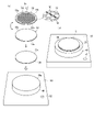
Images


Classifications
-
- H—ELECTRICITY
- H10—SEMICONDUCTOR DEVICES; ELECTRIC SOLID-STATE DEVICES NOT OTHERWISE PROVIDED FOR
- H10P—GENERIC PROCESSES OR APPARATUS FOR THE MANUFACTURE OR TREATMENT OF DEVICES COVERED BY CLASS H10
- H10P54/00—Cutting or separating of wafers, substrates or parts of devices
-
- B—PERFORMING OPERATIONS; TRANSPORTING
- B23—MACHINE TOOLS; METAL-WORKING NOT OTHERWISE PROVIDED FOR
- B23K—SOLDERING OR UNSOLDERING; WELDING; CLADDING OR PLATING BY SOLDERING OR WELDING; CUTTING BY APPLYING HEAT LOCALLY, e.g. FLAME CUTTING; WORKING BY LASER BEAM
- B23K26/00—Working by laser beam, e.g. welding, cutting or boring
- B23K26/36—Removing material
- B23K26/362—Laser etching
- B23K26/364—Laser etching for making a groove or trench, e.g. for scribing a break initiation groove
-
- B—PERFORMING OPERATIONS; TRANSPORTING
- B23—MACHINE TOOLS; METAL-WORKING NOT OTHERWISE PROVIDED FOR
- B23K—SOLDERING OR UNSOLDERING; WELDING; CLADDING OR PLATING BY SOLDERING OR WELDING; CUTTING BY APPLYING HEAT LOCALLY, e.g. FLAME CUTTING; WORKING BY LASER BEAM
- B23K26/00—Working by laser beam, e.g. welding, cutting or boring
- B23K26/36—Removing material
- B23K26/40—Removing material taking account of the properties of the material involved
-
- C—CHEMISTRY; METALLURGY
- C09—DYES; PAINTS; POLISHES; NATURAL RESINS; ADHESIVES; COMPOSITIONS NOT OTHERWISE PROVIDED FOR; APPLICATIONS OF MATERIALS NOT OTHERWISE PROVIDED FOR
- C09J—ADHESIVES; NON-MECHANICAL ASPECTS OF ADHESIVE PROCESSES IN GENERAL; ADHESIVE PROCESSES NOT PROVIDED FOR ELSEWHERE; USE OF MATERIALS AS ADHESIVES
- C09J7/00—Adhesives in the form of films or foils
- C09J7/20—Adhesives in the form of films or foils characterised by their carriers
- C09J7/22—Plastics; Metallised plastics
- C09J7/24—Plastics; Metallised plastics based on macromolecular compounds obtained by reactions involving only carbon-to-carbon unsaturated bonds
- C09J7/241—Polyolefin, e.g.rubber
-
- H—ELECTRICITY
- H10—SEMICONDUCTOR DEVICES; ELECTRIC SOLID-STATE DEVICES NOT OTHERWISE PROVIDED FOR
- H10P—GENERIC PROCESSES OR APPARATUS FOR THE MANUFACTURE OR TREATMENT OF DEVICES COVERED BY CLASS H10
- H10P52/00—Grinding, lapping or polishing of wafers, substrates or parts of devices
-
- H—ELECTRICITY
- H10—SEMICONDUCTOR DEVICES; ELECTRIC SOLID-STATE DEVICES NOT OTHERWISE PROVIDED FOR
- H10P—GENERIC PROCESSES OR APPARATUS FOR THE MANUFACTURE OR TREATMENT OF DEVICES COVERED BY CLASS H10
- H10P72/00—Handling or holding of wafers, substrates or devices during manufacture or treatment thereof
- H10P72/70—Handling or holding of wafers, substrates or devices during manufacture or treatment thereof for supporting or gripping
- H10P72/74—Handling or holding of wafers, substrates or devices during manufacture or treatment thereof for supporting or gripping using temporarily an auxiliary support
- H10P72/7402—Wafer tapes, e.g. grinding or dicing support tapes
-
- H—ELECTRICITY
- H10—SEMICONDUCTOR DEVICES; ELECTRIC SOLID-STATE DEVICES NOT OTHERWISE PROVIDED FOR
- H10P—GENERIC PROCESSES OR APPARATUS FOR THE MANUFACTURE OR TREATMENT OF DEVICES COVERED BY CLASS H10
- H10P72/00—Handling or holding of wafers, substrates or devices during manufacture or treatment thereof
- H10P72/70—Handling or holding of wafers, substrates or devices during manufacture or treatment thereof for supporting or gripping
- H10P72/74—Handling or holding of wafers, substrates or devices during manufacture or treatment thereof for supporting or gripping using temporarily an auxiliary support
- H10P72/7416—Handling or holding of wafers, substrates or devices during manufacture or treatment thereof for supporting or gripping using temporarily an auxiliary support used during dicing or grinding
-
- H—ELECTRICITY
- H10—SEMICONDUCTOR DEVICES; ELECTRIC SOLID-STATE DEVICES NOT OTHERWISE PROVIDED FOR
- H10P—GENERIC PROCESSES OR APPARATUS FOR THE MANUFACTURE OR TREATMENT OF DEVICES COVERED BY CLASS H10
- H10P72/00—Handling or holding of wafers, substrates or devices during manufacture or treatment thereof
- H10P72/70—Handling or holding of wafers, substrates or devices during manufacture or treatment thereof for supporting or gripping
- H10P72/74—Handling or holding of wafers, substrates or devices during manufacture or treatment thereof for supporting or gripping using temporarily an auxiliary support
- H10P72/7422—Handling or holding of wafers, substrates or devices during manufacture or treatment thereof for supporting or gripping using temporarily an auxiliary support used to protect an active side of a device or wafer
Landscapes
- Engineering & Computer Science (AREA)
- Physics & Mathematics (AREA)
- Optics & Photonics (AREA)
- Chemical & Material Sciences (AREA)
- Plasma & Fusion (AREA)
- Mechanical Engineering (AREA)
- Chemical Kinetics & Catalysis (AREA)
- Organic Chemistry (AREA)
- Dicing (AREA)
- Perforating, Stamping-Out Or Severing By Means Other Than Cutting (AREA)
- Processing Of Stones Or Stones Resemblance Materials (AREA)
- Laser Beam Processing (AREA)
Description
分割予定ラインにTEGが形成されたウエーハを加工するウエーハの加工方法に関する。 The present invention relates to a method for processing a wafer in which a TEG is formed on a planned division line.
IC、LSI等の複数のデバイスが分割予定ラインによって区画され表面に形成されたウエーハは、レーザー加工装置によって分割予定ラインに対応するウエーハの内部に改質層が形成され、外力が付与されて個々のデバイスに分割されて、携帯電話、パソコン等の電気機器に利用される(例えば、特許文献1を参照。)。 In a wafer in which a plurality of devices such as ICs and LSIs are partitioned by a scheduled division line and formed on the surface, a modified layer is formed inside the wafer corresponding to the scheduled division line by a laser processing device, and an external force is applied to each wafer. It is divided into the above-mentioned devices and used for electric devices such as mobile phones and personal computers (see, for example, Patent Document 1).
また、デバイスの評価、解析に用いられるTEG(Test Element Gruoup)と称される金属片が分割予定ラインに形成されているウエーハを個々のデバイスに分割する場合は、TEGが形成された分割予定ラインの上面にレーザー光線の集光点を位置付けて照射し、TEGを切断する必要がある。 In addition, when a wafer in which a metal piece called TEG (Test Element Group) used for device evaluation and analysis is formed in a planned division line is divided into individual devices, the planned division line in which the TEG is formed is formed. It is necessary to position the condensing point of the laser beam on the upper surface of the wafer and irradiate it to cut the TEG.
上記したTEGを分割予定ラインに沿って切断すべくウエーハの上面側からレーザー光線の集光点をTEGに位置付けて照射してアブレーション加工を実施すると、レーザー光線が照射された位置からデブリが飛散して集光レンズが汚染されるという問題がある。 When the above-mentioned TEG is cut along the scheduled division line by irradiating the TEG with the condensing point of the laser beam positioned on the TEG from the upper surface side of the wafer, debris is scattered and collected from the position irradiated with the laser beam. There is a problem that the optical lens is contaminated.
また、デブリの飛散を抑制するためにウエーハの表面に保護テープを貼着してレーザー光線を照射すると、保護テープを貼着する際に用いられる糊剤が保護テープを剥離した後にウエーハの表面に付着して残存し、デバイスの品質を低下させるという問題がある。特に、内部に改質層を形成するウエーハに対して透過性を有する波長のレーザー光線を用いてアブレーション加工を実施することでTEGを切断する場合に、このような汚染の問題が生じる。 In addition, when a protective tape is attached to the surface of the wafer and irradiated with a laser beam to suppress the scattering of debris, the adhesive used when attaching the protective tape adheres to the surface of the wafer after the protective tape is peeled off. There is a problem that the quality of the device is deteriorated. In particular, when the TEG is cut by performing ablation processing using a laser beam having a wavelength that is transparent to the wafer forming the modified layer inside, such a problem of contamination arises.
本発明は、上記事実に鑑みなされたものであり、その主たる技術課題は、分割予定ラインにTEGが形成されたウエーハに対しレーザー光線を照射して加工する際にも、集光レンズを汚染することなく、デバイスの品質も低下させることのないウエーハの加工方法を提供することにある。 The present invention has been made in view of the above facts, and the main technical problem thereof is to contaminate the condenser lens even when processing by irradiating a wafer on which a TEG is formed on a planned division line with a laser beam. It is an object of the present invention to provide a method for processing a wafer without deteriorating the quality of the device.
上記主たる技術課題を解決するため、本発明によれば、複数のデバイスが分割予定ラインによって区画されたデバイス領域が表面に形成されたウエーハを個々のデバイスに分割するウエーハの加工方法であって、少なくともデバイス領域を覆う大きさのポリオレフィン系シート、又はポリエステル系シートのいずれかのシートをウエーハの表面に敷設して熱圧着し、ウエーハの表面を該シートで保護するウエーハ表面保護工程と、シート側からレーザー光線の集光点をウエーハの分割予定ラインに位置付けて照射し分割予定ラインに形成されたTEGを切断するTEG切断工程と、ウエーハの裏面からウエーハに対して透過性を有する波長のレーザー光線の集光点を分割予定ラインに対応する内部に位置付けて照射し分割予定ラインに沿って改質層を形成する改質層形成工程と、該TEG切断工程と該改質層形成工程とを実施した後、ウエーハに外力を付与し、ウエーハを個々のデバイスに分割するウエーハ分割工程と、から少なくとも構成されるウエーハの加工方法が提供される。 In order to solve the above-mentioned main technical problem, according to the present invention, there is a method for processing a wafer in which a wafer having a device region partitioned by a planned division line is divided into individual devices. A wafer surface protection step in which a sheet of either a polyolefin-based sheet or a polyester-based sheet having a size that covers at least the device area is laid on the surface of the wafer and thermocompression bonded is performed to protect the surface of the wafer with the sheet, and the sheet side. A TEG cutting process that positions the condensing point of the laser beam from the wafer on the planned division line of the wafer and irradiates it to cut the TEG formed on the scheduled division line, and a collection of laser beams with a wavelength that is transparent to the wafer from the back surface of the wafer. After performing the modified layer forming step of irradiating the light spots in the position corresponding to the planned dividing line to form the modified layer along the planned dividing line, and the TEG cutting step and the modified layer forming step. , A wafer dividing step of applying an external force to a wafer and dividing the wafer into individual devices, and a method for processing the wafer, which is composed of at least a wafer, are provided.
好ましくは、該TEG切断工程の前又は後に、ウエーハの裏面をダイシングテープに貼着すると共にウエーハを収容する開口を有するフレームを貼着してダイシングテープを介してウエーハをフレームで支持するフレーム支持工程を含み、該改質層形成工程において、ダイシングテープ越しにレーザー光線を照射する。また、該ウエーハの分割工程の前に該ウエーハの表面から該シートを剥離することが好ましい。さらに、該TEG切断工程で使用するレーザー光線は、該改質層形成工程で使用されるレーザー光線と同じにすることができる。 Preferably, before or after the TEG cutting step, the back surface of the wafer is attached to the dicing tape, and a frame having an opening for accommodating the wafer is attached to support the wafer with the frame via the dicing tape. In the step of forming the modified layer, a laser beam is irradiated through the dicing tape. Further, it is preferable to peel off the sheet from the surface of the wafer before the dividing step of the wafer. Further, the laser beam used in the TEG cutting step can be the same as the laser beam used in the modified layer forming step.
該ポリオレフィン系のシートは、ポリエチレンシート、ポリプロピレンシート、ポリスチレンシートのいずれかで構成することができ、該シートとしてポリオレフィン系のシートが選択された場合の該シート熱圧着工程における該シートの加熱温度は、該シートがポリエチレンシートで構成される場合は120~140℃であり、該シートがポリプロピレンシートで構成される場合は160~180℃であり、該シートがポリスチレンシートで構成される場合は220~240℃とすることがこのましい。 The polyolefin-based sheet can be composed of any of a polyethylene sheet, a polypropylene sheet, and a polystyrene sheet, and when the polyolefin-based sheet is selected as the sheet, the heating temperature of the sheet in the sheet thermocompression bonding step is set. When the sheet is composed of a polyethylene sheet, the temperature is 120 to 140 ° C., when the sheet is composed of a polypropylene sheet, the temperature is 160 to 180 ° C., and when the sheet is composed of a polystyrene sheet, the temperature is 220 to 1. It is preferable to set the temperature to 240 ° C.
該ポリエステル系のシートは、ポリエチレンテレフタレートシート、ポリエチレンナフタレートシート、のいずれかで構成することができ、該シートとしてポリエステル系のシートが選択された場合の該シート熱圧着工程における該シートの加熱温度は、該シートがポリエチレンテレフタレートシートで構成される場合は250~270℃であり、該シートがポリエチレンナフタレートシートで構成される場合は160~180℃とすることが好ましい。 The polyester-based sheet can be composed of either a polyethylene terephthalate sheet or a polyethylene naphthalate sheet, and the heating temperature of the sheet in the sheet thermocompression bonding step when the polyester-based sheet is selected as the sheet. Is preferably 250 to 270 ° C. when the sheet is composed of a polyethylene terephthalate sheet, and is preferably 160 to 180 ° C. when the sheet is composed of a polyethylene naphthalate sheet.
本発明のウエーハの加工装置は、複数のデバイスが分割予定ラインによって区画されたデバイス領域が表面に形成されたウエーハを個々のデバイスに分割するウエーハの加工方法であって、少なくともデバイス領域を覆う大きさのポリオレフィン系シート、又はポリエステル系シートのいずれかのシートをウエーハの表面に敷設して熱圧着し、ウエーハの表面を該シートで保護するウエーハ表面保護工程と、シート側からレーザー光線の集光点をウエーハの分割予定ラインに位置付けて照射し分割予定ラインに形成されたTEGを切断するTEG切断工程と、ウエーハの裏面からウエーハに対して透過性を有する波長のレーザー光線の集光点を分割予定ラインに対応する内部に位置付けて照射し分割予定ラインに沿って改質層を形成する改質層形成工程と、該TEG切断工程と該改質層形成工程とを実施した後、ウエーハに外力を付与し、ウエーハを個々のデバイスに分割するウエーハ分割工程と、から少なくとも構成されていることから、TEGにレーザー光線を照射して切断する際に、熱圧着されたシートによってデブリの飛散が抑制され集光レンズの汚染を防止することができる。また、シートは熱圧着によってウエーハと一体化されていることから、ウエーハの表面から該シートを剥離しても、糊剤、ワックス、液状樹脂等がデバイスに残存するという問題が生じ得ず、デバイスの品質を低下させるという問題が解消される。 The wafer processing apparatus of the present invention is a method for processing a wafer in which a plurality of devices are divided by a planned division line and a wafer having a device area formed on the surface thereof is divided into individual devices, and is large enough to cover at least the device area. A wafer surface protection step in which either a wafer-based sheet or a polyester-based sheet is laid on the surface of a wafer and thermocompression bonded to protect the surface of the wafer with the sheet, and a light-collecting point of a laser beam from the sheet side. Is positioned at the planned division line of the wafer and irradiated to cut the TEG formed on the planned division line, and the condensing point of the laser beam having a wavelength that is transparent to the wafer from the back surface of the wafer is divided into the planned division line. After performing the modified layer forming step of forming the modified layer along the planned division line by irradiating the wafer at the position corresponding to the inside, the TEG cutting step and the modified layer forming step, an external force is applied to the wafer. However, since it is composed of at least a wafer dividing process that divides the wafer into individual devices, when the TEG is irradiated with a laser beam for cutting, the thermocompression-bonded sheet suppresses the scattering of debris and condenses the wafer. It is possible to prevent the lens from being contaminated. Further, since the sheet is integrated with the wafer by thermocompression bonding, even if the sheet is peeled off from the surface of the wafer, there cannot be a problem that adhesive, wax, liquid resin, etc. remain in the device, and the device. The problem of degrading the quality of the product is solved.
以下、本発明に基づき構成されたウエーハの加工方法の実施形態について、添付図面を参照しながら詳細に説明する。 Hereinafter, embodiments of a wafer processing method configured based on the present invention will be described in detail with reference to the accompanying drawings.
本実施形態のウエーハの加工方法を実施するに際し、まず、図1(a)に示すように、ウエーハ10、及びシート20を用意する。ウエーハ10はSiC基板からなり、表面10aには、複数のデバイス12が分割予定ライン14によって区画されるデバイス領域10cが形成され、デバイス領域10cは、デバイス12が形成されない外周領域10dに囲繞されている。説明の都合上、図1(a)に示すウエーハ10の全体斜視図では省略しているが、右方にウエーハ10のデバイス領域10cの一部を拡大して示すように、分割予定ライン14上の一部には、デバイス12の評価、解析に用いられる金属片であるTEG16が形成されている。シート20は、例えば、ウエーハ10と略同形状に設定されており、ポリオレフィン系シート、又はポリエステル系シートによって構成される。本実施形態では、シート20としてポリオレフィン系のポリエチレン(PE)シートを選択している。なお、シート20の大きさは必ずしもウエーハ10と同形状である必要はなく、少なくともデバイス領域10cを覆う大きさであればよい。
In carrying out the wafer processing method of the present embodiment, first, as shown in FIG. 1A, a
(ウエーハ表面保護工程)
ウエーハ10、及びシート20を用意したならば、図1(a)に示すように、ウエーハ10の裏面10bを上方に、すなわち、ウエーハ10の表面10aを下方に向けてシート20上に位置付け、支持テーブル40の上面に配設したシート20をウエーハ10の表面10aに敷設した状態とする(図1(b)を参照。)。支持テーブル40は、基台50上に配設されており、支持テーブル40の上面は平坦に形成され、フッ素樹脂で被覆されている。支持テーブル40の内部には、図2に示すように、加熱手段として電気ヒータ42が配設され、さらに、図示しない温度センサーが内蔵される。電気ヒータ42及び該温度センサーは、図示しない制御装置、及び電源に接続され、支持テーブル40を所望の温度に調整することが可能になっている。
(Wafer surface protection process)
If the
ウエーハ10の表面10aにシート20を敷設したならば、シート20をウエーハ10に熱圧着する。図2を参照しながら、以下に具体的に説明する。
If the
シート20をウエーハ10に熱圧着するためには、図2の各図に示す熱圧着装置60を利用する。熱圧着装置60は、支持テーブル40を含む密閉環境を形成するための密閉カバー部材62を備える。なお、図2では、内部の構成を説明する都合上、密閉カバー部材62のみ断面を示している。密閉カバー部材62は、基台50の上面全体を覆う箱型部材であり、上壁62a、及び上壁62aの外周端部から垂下される側壁62bから構成され、下方側は開放されている。上壁62aの中央には、押圧部材64の支持軸64aが貫通し、上下方向に進退させるための開口62cが形成されている。また、支持軸64aを上下に進退させつつ、密閉カバー部材62の内部空間Sを外部と遮断して密閉環境とすべく、支持軸64aの外周を支持する開口部62cにシール構造62dが形成される。支持軸64aの下端には、押圧プレート64bが配設されている。押圧プレート64bは、少なくともウエーハ10よりも大径であり、好ましくは支持テーブル40よりもやや大きい寸法に設定された円盤形状である。密閉カバー部材62の側壁62bの下端面には、全周にわたって弾性シール部材62eが配設されている。また、図示は省略するが、押圧部材64の上方には、押圧部材64を上下方向に進退させるための駆動手段が配設される。
In order to thermocompression-bond the
上記したように、ウエーハ10の表面10aにシート20を敷設し、すなわち、ウエーハ10の裏面10bを上にしてシート20を介して支持テーブル40上に載置したならば、図2(a)に示すように基台50上に位置付けられた密閉カバー部材62を下降させて、基台50上に載置する。このとき、押圧プレート64bは、図2(b)に示すように、ウエーハ10の上面に接触しない上方位置に引き上げられている。密閉カバー部材62が基台50上に載置されると、側壁62bの下端面に配設された弾性シール部材62eが基台50の上面に密着する。基台50における支持テーブル40の近傍位置には、吸引孔52が配設されており、吸引孔52を介して、密閉カバー部材62によって形成される内部空間Sに吸引手段が接続される。
As described above, if the
図2(b)に示すように、密閉カバー部材62を基台50上に載置し、密閉カバー部材62の内部空間Sが密閉環境とされたならば、図示しない吸引手段を作動して、吸引孔52を介して内部空間Sの空気を吸引し、ウエーハ10を含む領域を真空に近い状態まで減圧する。これと同時に、電気ヒータ42を作動させて、ウエーハ10を支持しているシート20を加熱する。支持テーブル40の電気ヒータ42を作動させ、図示しない温度センサーによって支持テーブル40の温度を制御することにより、シート20を構成するポリエチレンシートが融点近傍の温度(120~140℃)になるように加熱する。さらに、シート20を加熱すると同時に、図2(c)に示すように、押圧プレート64bを下降させてウエーハ10の上面全体を均等な力で押圧する。ウエーハ10を収容している内部空間Sが減圧されることにより、ウエーハ10とシート20との間に残存する空気も吸引されて除去される。そして、シート20は、上記した温度に加熱されることにより軟化して粘着性が増し、シート20とウエーハ10とが熱圧着されて一体化ユニットWが形成され、ウエーハ表面保護工程が完了する。このウエーハ表面保護工程を実施することにより、ウエーハ10の表面10aに形成されたデバイス領域10cがシート20により覆われ、保護された状態となる。
As shown in FIG. 2B, when the sealing
上記したウエーハ表面保護工程が完了したならば、図示しない吸引手段、及び電気ヒータ42を停止し、押圧プレート64bを上昇させると共に、密閉カバー部材62を上方に引き上げる。シート20の温度が常温近傍まで低下したならば、支持テーブル40から一体化ユニットWを搬出することができる。本実施形態では、支持テーブル40の上面にフッ素樹脂が被覆されていることから、加熱されることにより粘着性が増したシート20であったとしても、支持テーブル40から容易に剥離される。
When the wafer surface protection step described above is completed, the suction means (not shown) and the
上記したウエーハ表面保護工程を実施することにより形成された一体化ユニットWについて、図3を参照しながら、さらに説明する。上記したように、ウエーハ表面保護工程によれば、密閉環境内で減圧した状態で、シート20を加熱し、シート20が軟化した状態でウエーハ10を押圧して一体化させるため、ウエーハ10は、糊剤やワックス等を介することなくシート20に十分な支持力で支持される。さらに、ウエーハ10の表面10aに形成されている分割予定ライン14にTEG16が形成されている場合、TEG16の近傍からも完全に空気が吸引されて除去され、図中に一体化ユニットWの一部の断面を拡大して示すように、加熱されて軟化した状態のシート20にデバイス12、及びTEG16が埋設され密着して一体化される。
The integrated unit W formed by carrying out the above-mentioned wafer surface protection step will be further described with reference to FIG. As described above, according to the wafer surface protection step, the
(TEG切断工程)
上記したウエーハ表面保護工程を実施したならば、次いで、分割予定ライン14に形成されたTEG16を切断するTEG切断工程を実施する。以下に、TEG切断工程についてより具体的に説明する。
(TEG cutting process)
After the above-mentioned wafer surface protection step is carried out, a TEG cutting step for cutting the
熱圧着装置60の支持テーブル40から剥離された一体化ユニットWは、図4に示すように、ウエーハ10の裏面10bを下方に向けてダイシングテープTに貼着されると共に、ウエーハ10を収容する開口部を有するフレームFにダイシングテープTの外周部が貼着されて支持される(フレーム支持工程)。
As shown in FIG. 4, the integrated unit W peeled off from the support table 40 of the
一体化ユニットWがフレームFに支持されたならば、図5(a)に示す周知のレーザー加工装置70(一部のみ示す。)に搬送し、ダイシングテープT側を下にして図示しない保持手段に保持させる。該保持手段に一体化ユニットWを保持させたならば、図示しない撮像カメラ等を含むアライメント手段を用いて、レーザー光線照射手段72から照射されるレーザー光線LBの照射位置と被照射位置との位置合わせを行うアライメントを実施する。 When the integrated unit W is supported by the frame F, it is conveyed to a well-known laser processing device 70 (only a part thereof is shown) shown in FIG. 5A, and a holding means (not shown) with the dicing tape T side facing down. To hold it. When the integrated unit W is held by the holding means, the alignment means of the laser beam LB irradiated from the laser beam irradiating means 72 and the irradiated position are aligned by using an alignment means including an image pickup camera (not shown). Perform the alignment to be performed.
上記したアライメントを実施したならば、レーザー光線照射手段72に配設された集光レンズ72aを介して照射されるレーザー光線LBの集光点をウエーハ10上の所定の加工開始位置の表面に位置付ける。次いで、レーザー光線LBを照射しながら、矢印Xで示す方向にウエーハ10を移動させることにより、シート20越しにウエーハ10の分割予定ライン14に沿ってレーザー光線を照射する。これにより、分割予定ライン14に沿ってアブレーション加工が施され、レーザー加工溝100が形成されると共に、上記したTEG16が切断される。そして、ウエーハ10が保持された保持手段を、図示しない移動手段により、X方向、Y方向、回転方向に適宜移動させることで、図5(b)に示すように、ウエーハ10の全ての分割予定ライン14にレーザー光線LBを照射してアブレーション加工を施し、分割予定ライン14上のTEG16が切断される。このように、TEG切断工程におけるレーザー光線LBの照射は、ウエーハ10の表面10aに熱圧着されたシート20越しに実施されるため、アブレーション加工により発生するデブリの飛散がシート20によって妨げられ、集光レンズ72aの汚染が抑制される。以上により、TEG切断工程が完了する。
When the above alignment is performed, the condensing point of the laser beam LB irradiated through the condensing
なお、上記TEG切断工程を実施する際のレーザー加工条件は、例えば、以下のように設定される。
波長 :1064nm
繰り返し周波数 :60kHz
平均出力 :1W
送り速度(V) :600mm/秒
The laser processing conditions for carrying out the TEG cutting step are set as follows, for example.
Wavelength: 1064 nm
Repeat frequency: 60kHz
Average output: 1W
Feed rate (V): 600 mm / sec
上記したTEG切断工程が実施されたならば、次いで、改質層形成工程を実施する。以下に改質層形成工程についてより具体的に説明する。 After the above-mentioned TEG cutting step is carried out, the modified layer forming step is then carried out. The modified layer forming step will be described in more detail below.
(改質層形成工程)
本実施形態の改質層形成工程は、上記したレーザー加工装置70をそのまま使用することができる。レーザー加工装置70によって上記したTEG切断工程が実施されたウエーハ10は、図示しない保持手段から一旦取り出される。そして、図6に示すように、ダイシングテープTを介して保持された一体化ユニットWをフレームFごと裏返し、一体化ユニットW側を下にして、すなわち、ダイシングテープT側を上にして、再び保持手段に保持させる。保持手段に一体化ユニットWを保持させたならば、図示しないアライメント手段により、レーザー光線LBの照射位置と、ウエーハ10の分割予定ライン14との位置合わせを実施する。なお、図6に示すように、改質層形成工程は、ウエーハ10の裏面10b側からレーザー光線LBを照射するものであり、ウエーハ10の表面10a側が下に向けられていることから、アライメント手段には、図示しない赤外線照射手段と赤外線撮像手段を備え、裏面10b側から分割予定ライン14を確認してアライメントを実施することが可能に構成されている。
(Modified layer forming process)
In the modified layer forming step of the present embodiment, the above-mentioned
上記したアライメントを実施したならば、レーザー光線照射手段72を作動させてレーザー光線LBの集光点をウエーハ10の分割予定ライン14に対応する内部に位置付ける。次いで、ダイシングテープT越しにレーザー光線LBを照射しながら、矢印Xで示す方向にウエーハ10を移動させる。本実施形態のレーザー光線照射手段72から照射されるレーザー光線LBは、上記したレーザー加工条件で示したように、ウエーハ10を構成するSiCに対して透過性を有する波長(=1064nm)であることにより、分割予定ライン14の内部に、ウエーハ10の分割起点となる改質層110を形成する。そして、ウエーハ10が保持された保持手段を、上記したTEG切断工程と同様に、X方向、Y方向、回転方向に適宜移動させることで、ウエーハ10の全ての分割予定ライン14に沿って、その内部に改質層110を形成する。以上により改質層形成工程が完了する。
After the above alignment is performed, the laser beam irradiating means 72 is operated to position the condensing point of the laser beam LB inside the
(ウエーハ分割工程)
上記した改質層形成工程を実施したならば、ウエーハ10に外力を付与してウエーハ10を個々のデバイス12に分割するウエーハ分割工程を実施する。以下に、ウエーハ分割工程についてより具体的に説明する。
(Wafer division process)
After the above-mentioned modified layer forming step is carried out, the wafer dividing step of applying an external force to the
ウエーハ分割工程を実施する前に、まず、図7に示すように、フレームFに支持されたウエーハ10から、シート20を剥離する。シート20を剥離する際にシート20を加熱すれば、シート20が軟化するため、より容易に剥離させることが可能になる。また、シート20をウエーハ10から剥離する際に冷却することによってシート20の粘着力が低下する場合もあり、シート20を冷却してから剥離工程を実施してもよい。シート20の剥離を実施する際に、シート20を加熱するか、冷却するかについては、シート20を構成する素材の特性に応じて選択すればよい。本実施形態では、上記したように、ウエーハ10を、熱圧着によりシート20に支持させており、シート20とウエーハ10の間に、液状樹脂、糊剤、ワックス等を介在させていない。よって、ウエーハ10の表面10aからシート20を剥離しても、ウエーハ10の表面10a、すなわち、デバイス12に液状樹脂、糊剤、ワックス等が残存することがなく、デバイス12の品質を低下させるという問題が発生しない。
Before carrying out the wafer dividing step, first, as shown in FIG. 7, the
ウエーハ10からシート20を剥離したならば、図8に示すウエーハ分割工程を実施するための分割装置80に搬送する。分割装置80によってウエーハ分割工程を実施する具体的な態様について、以下に説明する。
After the
ウエーハ分割工程は、図8にその一部を断面で示す分割装置80によって実施されるものであり、分割装置80は、フレーム保持部材81と、その上面部にフレームFを載置してフレームFを保持するクランプ82と、クランプ82により保持されたフレームFに装着されたウエーハ10を拡張するための少なくとも上方が開口した円筒形状からなる拡張ドラム83とを備えている。フレーム保持部材81は、拡張ドラム83を囲むように設置された複数のエアシリンダ84aと、エアシリンダ84aから延びるピストンロッド84bとから構成される支持手段84により昇降可能に支持されている。
The wafer dividing step is carried out by a dividing
拡張ドラム83は、フレームFの内径よりも小さく、フレームFに装着されたダイシングテープTに貼着されるウエーハ10の外径よりも大きく設定されている。ここで、図8に示すように、分割装置80は、フレーム保持部材81と、拡張ドラム83の上面部が略同一の高さになる位置(点線で示す)と、支持手段84の作用によりフレーム保持部材81が下降させられ、拡張ドラム83の上端部が、フレーム保持部材81の上端部よりも相対的に高くなる位置(実線で示す)と、にすることができる。
The
フレーム保持部材81を下降させて、拡張ドラム83の上端を、点線で示す位置から、実線で示す高い位置になるように相対的に変化させると、フレームFに装着された粘着テープTは拡張ドラム83の上端縁によって拡張させられる。この結果、ダイシングテープTに貼着されているウエーハ10には放射状に外力(引張力)が作用するため、上述したTEG切断工程、及び改質層形成工程において形成されたレーザー加工溝100、及び改質層110に沿って個々のデバイス12に分割される。以上により、ウエーハ分割工程が完了する。
When the
上記したウエーハ分割工程が完了し、個々のデバイス12が分割され、離反されたならば、ピックアップコレット85を作動させて間隔が広げられた状態のデバイス12を吸着し、ダイシングテープTから剥離して、次工程に搬送、又は、図示しない収容ケースに収容する。以上により、本実施形態におけるウエーハの加工方法が完了する。
When the above-mentioned wafer division step is completed and the
本実施形態では、上記した分割装置80によってウエーハ10に放射状に作用する外力を付与し、個々のデバイス12に分割したが、ウエーハ10に外力を付与して個々のデバイス12に分割する手段はこれに限定されない。例えば、楔状部材を分割予定ライン14に沿って押圧して外力を付与することによってウエーハ10を分割したり、ローラ状の押圧手段によってウエーハ10を上方から押圧し外力を付与してウエーハ10を個々のデバイス12に分割したりすることも可能である。
In the present embodiment, the
本実施形態では、TEG切断工程で照射するレーザー光線を、改質層形成工程において照射するレーザー光線と同一のレーザー光線を照射することとし、集光点位置を分割予定ライン14の表面位置に調整することでアブレーション加工を施し、TEGを切断している。これにより、TEG切断工程を実施する際に、改質層形成工程で作動するレーザー光線照射手段72とは別のレーザー光線照射手段を用意する必要がなく、経済的である。ただし、本発明はこれに限定されるものではなく、TEGを切断することが可能な別の波長のレーザー光線を照射することができる他のレーザー光線照射手段を用意して。TEG切断工程において照射することを除外しない。
In the present embodiment, the laser beam irradiated in the TEG cutting step is irradiated with the same laser beam as the laser beam irradiated in the modified layer forming step, and the position of the condensing point is adjusted to the surface position of the scheduled
本実施形態では、ダイシングテープTを介してウエーハ10をフレームFに支持させるフレーム支持工程を、TEG切断工程の前に実施したが、本発明はこれに限定されず、TEG切断工程の後に実施するようにしてもよい。
In the present embodiment, the frame support step of supporting the
上記した実施形態では、ポリエチレンシートによりシート20を構成したが、本発明はこれに限定されない。液状樹脂、糊剤、ワックス等を必要とせず、熱圧着によりウエーハ10の表面を保護可能なシート20としては、ポリオレフィン系シート、ポリエステル系シートの中から適宜選択することができる。ポリオレフィン系シートとしては、上記したポリエチレンシートの他、例えば、ポリプロピレン(PP)シート、ポリスチレン(PS)シートを選択することができる。また、ポリエステル系シートとしては、例えば、ポリエチレンテレフタレート(PET)シート、ポリエチレンナフタレート(PEN)シートを選択することができる。
In the above embodiment, the
上記した実施形態では、ウエーハ表面保護工程においてシート20を熱圧着する際の加熱温度を、ポリエチレンシートの融点近傍の温度(120~140℃)に設定したが、上記したように、シート20として他のシートを選択して構成する場合は、選択したシートの素材の融点近傍の温度になるように加熱することが好ましい。例えば、シート20がポリプロピレンシートで構成される場合は、加熱する際の温度設定を160~180℃とし、シート20がポリスチレンシートで構成される場合は、加熱する際の温度を220~240℃とすることが好ましい。また、シート20がポリエチレンテレフタレートシートで構成される場合は、加熱する際の温度を250~270℃とし、シート20がポリエチレンナフタレートシートで構成される場合は、加熱する際の温度を160~180℃に設定することが好ましい。
In the above-described embodiment, the heating temperature at which the
また、上記した実施形態では、密閉カバー部材62により密閉環境を形成したが、本発明はこれに限定されない。例えば、図9(a)に示すように、ウエーハ10をシート20と共にシート20よりも大きい吸着チャック91を有する保持手段90に保持させ、吸着チャック91の上面全体をフィルム状部材200で覆い、吸着チャック91から負圧Vmを作用させることで、ウエーハ10を含むフィルム状部材200の内側を密閉環境とし、該密閉環境内の空間を減圧することができる。そして、図9(b)に一部拡大断面図として示すように、図示しない加熱手段を備えたローラ210により、シート20を所望の温度に加熱しながら、フィルム状部材200の上からウエーハ10の裏面10b全体を押圧することで、本発明のシート熱圧着工程を実施することも可能である。
Further, in the above-described embodiment, the closed environment is formed by the
10:ウエーハ
12:デバイス
14:分割予定ライン
16:TEG
20:シート
40:支持テーブル
42:電気ヒータ
50:基台
52:吸引孔
60:熱圧着装置
62:密閉カバー部材
64:押圧部材
64a:押圧プレート
70:レーザー加工装置
72:レーザー光線照射手段
72a:集光レンズ
80:分割装置
100:レーザー加工溝
110:改質層
200:フィルム状部材
210:ローラ
10: Wafer 12: Device 14: Scheduled division line 16: TEG
20: Sheet 40: Support table 42: Electric heater 50: Base 52: Suction hole 60: Thermocompression bonding device 62: Sealed cover member 64: Pressing
Claims (8)
少なくともデバイス領域を覆う大きさのポリオレフィン系シート、又はポリエステル系シートのいずれかのシートをウエーハの表面に敷設して熱圧着し、ウエーハの表面を該シートで保護するウエーハ表面保護工程と、
シート側からレーザー光線の集光点をウエーハの分割予定ラインに位置付けて照射し分割予定ラインに形成されたTEGを切断するTEG切断工程と、
ウエーハの裏面からウエーハに対して透過性を有する波長のレーザー光線の集光点を分割予定ラインに対応する内部に位置付けて照射し分割予定ラインに沿って改質層を形成する改質層形成工程と、
該TEG切断工程と該改質層形成工程とを実施した後、ウエーハに外力を付与し、ウエーハを個々のデバイスに分割するウエーハ分割工程と、
から少なくとも構成されるウエーハの加工方法。 A method of processing a wafer in which a wafer having a device area partitioned by a planned division line for a plurality of devices is divided into individual devices.
A wafer surface protection step in which a sheet of either a polyolefin-based sheet or a polyester-based sheet having a size that at least covers the device area is laid on the surface of the wafer and thermocompression bonded to protect the surface of the wafer with the sheet.
A TEG cutting process in which the condensing point of the laser beam is positioned on the scheduled division line of the wafer from the sheet side and irradiated to cut the TEG formed on the scheduled division line.
A modified layer forming step of irradiating the condensing point of a laser beam having a wavelength that is transparent to the wafer from the back surface of the wafer to the inside corresponding to the planned division line to form a modified layer along the planned division line. ,
After performing the TEG cutting step and the modified layer forming step, an external force is applied to the wafer to divide the wafer into individual devices, and a wafer dividing step.
Wafer processing method consisting of at least.
該改質層形成工程において、ダイシングテープ越しにレーザー光線を照射する請求項1に記載のウエーハの加工方法。 Before or after the TEG cutting step, the back surface of the wafer is attached to the dicing tape, and a frame having an opening for accommodating the wafer is attached to support the wafer with the frame via the dicing tape.
The method for processing a wafer according to claim 1, wherein in the modified layer forming step, a laser beam is irradiated through the dicing tape.
Priority Applications (3)
| Application Number | Priority Date | Filing Date | Title |
|---|---|---|---|
| JP2018119122A JP7049941B2 (en) | 2018-06-22 | 2018-06-22 | Wafer processing method |
| US16/446,258 US11315833B2 (en) | 2018-06-22 | 2019-06-19 | Wafer processing method including a test element group (TEG) cutting step |
| DE102019208940.2A DE102019208940B4 (en) | 2018-06-22 | 2019-06-19 | WAFER PROCESSING METHODS |
Applications Claiming Priority (1)
| Application Number | Priority Date | Filing Date | Title |
|---|---|---|---|
| JP2018119122A JP7049941B2 (en) | 2018-06-22 | 2018-06-22 | Wafer processing method |
Publications (2)
| Publication Number | Publication Date |
|---|---|
| JP2019220657A JP2019220657A (en) | 2019-12-26 |
| JP7049941B2 true JP7049941B2 (en) | 2022-04-07 |
Family
ID=68806096
Family Applications (1)
| Application Number | Title | Priority Date | Filing Date |
|---|---|---|---|
| JP2018119122A Active JP7049941B2 (en) | 2018-06-22 | 2018-06-22 | Wafer processing method |
Country Status (3)
| Country | Link |
|---|---|
| US (1) | US11315833B2 (en) |
| JP (1) | JP7049941B2 (en) |
| DE (1) | DE102019208940B4 (en) |
Families Citing this family (12)
| Publication number | Priority date | Publication date | Assignee | Title |
|---|---|---|---|---|
| JP7201342B2 (en) | 2018-06-06 | 2023-01-10 | 株式会社ディスコ | Wafer processing method |
| JP2019220550A (en) * | 2018-06-19 | 2019-12-26 | 株式会社ディスコ | Processing method for wafer |
| JP7266402B2 (en) * | 2018-12-28 | 2023-04-28 | 株式会社ディスコ | Chip manufacturing method |
| JP7461118B2 (en) * | 2019-08-19 | 2024-04-03 | 株式会社ディスコ | Wafer processing method |
| JP7486973B2 (en) * | 2020-02-20 | 2024-05-20 | 株式会社ディスコ | Wafer processing method |
| JP7604155B2 (en) * | 2020-09-28 | 2024-12-23 | 株式会社ディスコ | Wafer Processing Method |
| JP7650691B2 (en) * | 2021-03-22 | 2025-03-25 | 株式会社ディスコ | Stacked wafer processing method |
| JP7749354B2 (en) * | 2021-06-21 | 2025-10-06 | 株式会社ディスコ | Processing method |
| JP7777937B2 (en) * | 2021-07-28 | 2025-12-01 | 株式会社ディスコ | Processing method of workpiece |
| JP7831964B2 (en) | 2021-08-02 | 2026-03-17 | 株式会社ディスコ | Wafer splitting method |
| JP7737881B2 (en) * | 2021-12-01 | 2025-09-11 | 株式会社ディスコ | Workpiece processing method and laser processing device |
| JP2024027913A (en) * | 2022-08-19 | 2024-03-01 | 株式会社ディスコ | Braking method |
Citations (1)
| Publication number | Priority date | Publication date | Assignee | Title |
|---|---|---|---|---|
| JP2005340423A (en) | 2004-05-26 | 2005-12-08 | Renesas Technology Corp | Manufacturing method of semiconductor device |
Family Cites Families (10)
| Publication number | Priority date | Publication date | Assignee | Title |
|---|---|---|---|---|
| JP3408805B2 (en) * | 2000-09-13 | 2003-05-19 | 浜松ホトニクス株式会社 | Cutting origin region forming method and workpiece cutting method |
| JP2007012878A (en) * | 2005-06-30 | 2007-01-18 | Disco Abrasive Syst Ltd | Wafer division method |
| JP5363662B2 (en) * | 2011-09-30 | 2013-12-11 | リンテック株式会社 | Dicing sheet with protective film forming layer and chip manufacturing method |
| JP6178077B2 (en) * | 2013-01-23 | 2017-08-09 | 株式会社ディスコ | Wafer processing method |
| CN105143380B (en) * | 2013-03-28 | 2019-05-17 | 古河电气工业株式会社 | Adhesive tapes and tapes for wafer processing |
| JP6220644B2 (en) * | 2013-11-18 | 2017-10-25 | リンテック株式会社 | Chip manufacturing method |
| JP2017038030A (en) * | 2015-08-14 | 2017-02-16 | 株式会社ディスコ | Wafer processing method and electronic device |
| JP2016027678A (en) * | 2015-11-13 | 2016-02-18 | 株式会社ディスコ | Ablation processing method |
| JP2017107921A (en) * | 2015-12-07 | 2017-06-15 | 株式会社ディスコ | Wafer processing method |
| JP6713212B2 (en) * | 2016-07-06 | 2020-06-24 | 株式会社ディスコ | Method for manufacturing semiconductor device chip |
-
2018
- 2018-06-22 JP JP2018119122A patent/JP7049941B2/en active Active
-
2019
- 2019-06-19 US US16/446,258 patent/US11315833B2/en active Active
- 2019-06-19 DE DE102019208940.2A patent/DE102019208940B4/en active Active
Patent Citations (1)
| Publication number | Priority date | Publication date | Assignee | Title |
|---|---|---|---|---|
| JP2005340423A (en) | 2004-05-26 | 2005-12-08 | Renesas Technology Corp | Manufacturing method of semiconductor device |
Also Published As
| Publication number | Publication date |
|---|---|
| JP2019220657A (en) | 2019-12-26 |
| DE102019208940B4 (en) | 2025-05-08 |
| DE102019208940A1 (en) | 2019-12-24 |
| US11315833B2 (en) | 2022-04-26 |
| US20190393089A1 (en) | 2019-12-26 |
Similar Documents
| Publication | Publication Date | Title |
|---|---|---|
| JP7049941B2 (en) | Wafer processing method | |
| CN110783249B (en) | Wafer processing method | |
| CN110391139B (en) | Wafer processing method | |
| JP6208521B2 (en) | Wafer processing method | |
| JP2019192717A (en) | Method of processing wafer | |
| JP5378780B2 (en) | Tape expansion method and tape expansion device | |
| JP2007189057A (en) | Wafer dividing method and wafer dividing apparatus | |
| JP2010153692A (en) | Workpiece dividing method and tape expanding device | |
| JP6034219B2 (en) | Wafer processing method | |
| JP2019220550A (en) | Processing method for wafer | |
| TWI810309B (en) | Wafer processing method | |
| JP2017103406A (en) | Wafer processing method | |
| JP2007157887A (en) | Wafer division method | |
| JP6009240B2 (en) | Wafer processing method | |
| CN110429062B (en) | Wafer processing method | |
| JP6783620B2 (en) | Wafer processing method | |
| JP7154962B2 (en) | Plate-shaped object processing method | |
| JP2013041967A (en) | Division device | |
| CN111063631A (en) | wafer processing method | |
| JP2020115502A (en) | Wafer processing method | |
| JP2020064922A (en) | Wafer processing method | |
| JP7383338B2 (en) | Wafer processing method | |
| KR20230082571A (en) | Workpiece processing method and laser processing apparatus | |
| JP6751337B2 (en) | Method of breaking adhesive film | |
| JP2006059941A (en) | Manufacturing method of semiconductor chip |
Legal Events
| Date | Code | Title | Description |
|---|---|---|---|
| A621 | Written request for application examination |
Free format text: JAPANESE INTERMEDIATE CODE: A621 Effective date: 20210401 |
|
| TRDD | Decision of grant or rejection written | ||
| A977 | Report on retrieval |
Free format text: JAPANESE INTERMEDIATE CODE: A971007 Effective date: 20220303 |
|
| A01 | Written decision to grant a patent or to grant a registration (utility model) |
Free format text: JAPANESE INTERMEDIATE CODE: A01 Effective date: 20220308 |
|
| A61 | First payment of annual fees (during grant procedure) |
Free format text: JAPANESE INTERMEDIATE CODE: A61 Effective date: 20220328 |
|
| R150 | Certificate of patent or registration of utility model |
Ref document number: 7049941 Country of ref document: JP Free format text: JAPANESE INTERMEDIATE CODE: R150 |
|
| R250 | Receipt of annual fees |
Free format text: JAPANESE INTERMEDIATE CODE: R250 |