JP6991865B2 - Tft基板 - Google Patents
Tft基板 Download PDFInfo
- Publication number
- JP6991865B2 JP6991865B2 JP2018007271A JP2018007271A JP6991865B2 JP 6991865 B2 JP6991865 B2 JP 6991865B2 JP 2018007271 A JP2018007271 A JP 2018007271A JP 2018007271 A JP2018007271 A JP 2018007271A JP 6991865 B2 JP6991865 B2 JP 6991865B2
- Authority
- JP
- Japan
- Prior art keywords
- gate
- line
- gcl
- tft substrate
- transistor
- Prior art date
- Legal status (The legal status is an assumption and is not a legal conclusion. Google has not performed a legal analysis and makes no representation as to the accuracy of the status listed.)
- Active
Links
Images


Classifications
-
- H—ELECTRICITY
- H10—SEMICONDUCTOR DEVICES; ELECTRIC SOLID-STATE DEVICES NOT OTHERWISE PROVIDED FOR
- H10D—INORGANIC ELECTRIC SEMICONDUCTOR DEVICES
- H10D86/00—Integrated devices formed in or on insulating or conducting substrates, e.g. formed in silicon-on-insulator [SOI] substrates or on stainless steel or glass substrates
- H10D86/40—Integrated devices formed in or on insulating or conducting substrates, e.g. formed in silicon-on-insulator [SOI] substrates or on stainless steel or glass substrates characterised by multiple TFTs
- H10D86/421—Integrated devices formed in or on insulating or conducting substrates, e.g. formed in silicon-on-insulator [SOI] substrates or on stainless steel or glass substrates characterised by multiple TFTs having a particular composition, shape or crystalline structure of the active layer
-
- H—ELECTRICITY
- H10—SEMICONDUCTOR DEVICES; ELECTRIC SOLID-STATE DEVICES NOT OTHERWISE PROVIDED FOR
- H10D—INORGANIC ELECTRIC SEMICONDUCTOR DEVICES
- H10D30/00—Field-effect transistors [FET]
- H10D30/60—Insulated-gate field-effect transistors [IGFET]
- H10D30/67—Thin-film transistors [TFT]
- H10D30/6704—Thin-film transistors [TFT] having supplementary regions or layers in the thin films or in the insulated bulk substrates for controlling properties of the device
- H10D30/6713—Thin-film transistors [TFT] having supplementary regions or layers in the thin films or in the insulated bulk substrates for controlling properties of the device characterised by the properties of the source or drain regions, e.g. compositions or sectional shapes
-
- G—PHYSICS
- G02—OPTICS
- G02F—OPTICAL DEVICES OR ARRANGEMENTS FOR THE CONTROL OF LIGHT BY MODIFICATION OF THE OPTICAL PROPERTIES OF THE MEDIA OF THE ELEMENTS INVOLVED THEREIN; NON-LINEAR OPTICS; FREQUENCY-CHANGING OF LIGHT; OPTICAL LOGIC ELEMENTS; OPTICAL ANALOGUE/DIGITAL CONVERTERS
- G02F1/00—Devices or arrangements for the control of the intensity, colour, phase, polarisation or direction of light arriving from an independent light source, e.g. switching, gating or modulating; Non-linear optics
- G02F1/01—Devices or arrangements for the control of the intensity, colour, phase, polarisation or direction of light arriving from an independent light source, e.g. switching, gating or modulating; Non-linear optics for the control of the intensity, phase, polarisation or colour
- G02F1/13—Devices or arrangements for the control of the intensity, colour, phase, polarisation or direction of light arriving from an independent light source, e.g. switching, gating or modulating; Non-linear optics for the control of the intensity, phase, polarisation or colour based on liquid crystals, e.g. single liquid crystal display cells
- G02F1/133—Constructional arrangements; Operation of liquid crystal cells; Circuit arrangements
- G02F1/136—Liquid crystal cells structurally associated with a semi-conducting layer or substrate, e.g. cells forming part of an integrated circuit
- G02F1/1362—Active matrix addressed cells
- G02F1/1368—Active matrix addressed cells in which the switching element is a three-electrode device
-
- G—PHYSICS
- G02—OPTICS
- G02F—OPTICAL DEVICES OR ARRANGEMENTS FOR THE CONTROL OF LIGHT BY MODIFICATION OF THE OPTICAL PROPERTIES OF THE MEDIA OF THE ELEMENTS INVOLVED THEREIN; NON-LINEAR OPTICS; FREQUENCY-CHANGING OF LIGHT; OPTICAL LOGIC ELEMENTS; OPTICAL ANALOGUE/DIGITAL CONVERTERS
- G02F1/00—Devices or arrangements for the control of the intensity, colour, phase, polarisation or direction of light arriving from an independent light source, e.g. switching, gating or modulating; Non-linear optics
- G02F1/01—Devices or arrangements for the control of the intensity, colour, phase, polarisation or direction of light arriving from an independent light source, e.g. switching, gating or modulating; Non-linear optics for the control of the intensity, phase, polarisation or colour
- G02F1/165—Devices or arrangements for the control of the intensity, colour, phase, polarisation or direction of light arriving from an independent light source, e.g. switching, gating or modulating; Non-linear optics for the control of the intensity, phase, polarisation or colour based on translational movement of particles in a fluid under the influence of an applied field
- G02F1/166—Devices or arrangements for the control of the intensity, colour, phase, polarisation or direction of light arriving from an independent light source, e.g. switching, gating or modulating; Non-linear optics for the control of the intensity, phase, polarisation or colour based on translational movement of particles in a fluid under the influence of an applied field characterised by the electro-optical or magneto-optical effect
- G02F1/167—Devices or arrangements for the control of the intensity, colour, phase, polarisation or direction of light arriving from an independent light source, e.g. switching, gating or modulating; Non-linear optics for the control of the intensity, phase, polarisation or colour based on translational movement of particles in a fluid under the influence of an applied field characterised by the electro-optical or magneto-optical effect by electrophoresis
-
- G—PHYSICS
- G09—EDUCATION; CRYPTOGRAPHY; DISPLAY; ADVERTISING; SEALS
- G09F—DISPLAYING; ADVERTISING; SIGNS; LABELS OR NAME-PLATES; SEALS
- G09F9/00—Indicating arrangements for variable information in which the information is built-up on a support by selection or combination of individual elements
- G09F9/30—Indicating arrangements for variable information in which the information is built-up on a support by selection or combination of individual elements in which the desired character or characters are formed by combining individual elements
-
- G—PHYSICS
- G09—EDUCATION; CRYPTOGRAPHY; DISPLAY; ADVERTISING; SEALS
- G09G—ARRANGEMENTS OR CIRCUITS FOR CONTROL OF INDICATING DEVICES USING STATIC MEANS TO PRESENT VARIABLE INFORMATION
- G09G3/00—Control arrangements or circuits, of interest only in connection with visual indicators other than cathode-ray tubes
- G09G3/20—Control arrangements or circuits, of interest only in connection with visual indicators other than cathode-ray tubes for presentation of an assembly of a number of characters, e.g. a page, by composing the assembly by combination of individual elements arranged in a matrix no fixed position being assigned to or needed to be assigned to the individual characters or partial characters
- G09G3/34—Control arrangements or circuits, of interest only in connection with visual indicators other than cathode-ray tubes for presentation of an assembly of a number of characters, e.g. a page, by composing the assembly by combination of individual elements arranged in a matrix no fixed position being assigned to or needed to be assigned to the individual characters or partial characters by control of light from an independent source
-
- H—ELECTRICITY
- H10—SEMICONDUCTOR DEVICES; ELECTRIC SOLID-STATE DEVICES NOT OTHERWISE PROVIDED FOR
- H10D—INORGANIC ELECTRIC SEMICONDUCTOR DEVICES
- H10D30/00—Field-effect transistors [FET]
- H10D30/60—Insulated-gate field-effect transistors [IGFET]
- H10D30/67—Thin-film transistors [TFT]
- H10D30/674—Thin-film transistors [TFT] characterised by the active materials
- H10D30/6755—Oxide semiconductors, e.g. zinc oxide, copper aluminium oxide or cadmium stannate
-
- H—ELECTRICITY
- H10—SEMICONDUCTOR DEVICES; ELECTRIC SOLID-STATE DEVICES NOT OTHERWISE PROVIDED FOR
- H10D—INORGANIC ELECTRIC SEMICONDUCTOR DEVICES
- H10D30/00—Field-effect transistors [FET]
- H10D30/60—Insulated-gate field-effect transistors [IGFET]
- H10D30/67—Thin-film transistors [TFT]
- H10D30/6757—Thin-film transistors [TFT] characterised by the structure of the channel, e.g. transverse or longitudinal shape or doping profile
-
- H—ELECTRICITY
- H10—SEMICONDUCTOR DEVICES; ELECTRIC SOLID-STATE DEVICES NOT OTHERWISE PROVIDED FOR
- H10D—INORGANIC ELECTRIC SEMICONDUCTOR DEVICES
- H10D86/00—Integrated devices formed in or on insulating or conducting substrates, e.g. formed in silicon-on-insulator [SOI] substrates or on stainless steel or glass substrates
- H10D86/40—Integrated devices formed in or on insulating or conducting substrates, e.g. formed in silicon-on-insulator [SOI] substrates or on stainless steel or glass substrates characterised by multiple TFTs
- H10D86/441—Interconnections, e.g. scanning lines
-
- H—ELECTRICITY
- H10—SEMICONDUCTOR DEVICES; ELECTRIC SOLID-STATE DEVICES NOT OTHERWISE PROVIDED FOR
- H10D—INORGANIC ELECTRIC SEMICONDUCTOR DEVICES
- H10D86/00—Integrated devices formed in or on insulating or conducting substrates, e.g. formed in silicon-on-insulator [SOI] substrates or on stainless steel or glass substrates
- H10D86/40—Integrated devices formed in or on insulating or conducting substrates, e.g. formed in silicon-on-insulator [SOI] substrates or on stainless steel or glass substrates characterised by multiple TFTs
- H10D86/451—Integrated devices formed in or on insulating or conducting substrates, e.g. formed in silicon-on-insulator [SOI] substrates or on stainless steel or glass substrates characterised by multiple TFTs characterised by the compositions or shapes of the interlayer dielectrics
-
- H—ELECTRICITY
- H10—SEMICONDUCTOR DEVICES; ELECTRIC SOLID-STATE DEVICES NOT OTHERWISE PROVIDED FOR
- H10D—INORGANIC ELECTRIC SEMICONDUCTOR DEVICES
- H10D86/00—Integrated devices formed in or on insulating or conducting substrates, e.g. formed in silicon-on-insulator [SOI] substrates or on stainless steel or glass substrates
- H10D86/40—Integrated devices formed in or on insulating or conducting substrates, e.g. formed in silicon-on-insulator [SOI] substrates or on stainless steel or glass substrates characterised by multiple TFTs
- H10D86/60—Integrated devices formed in or on insulating or conducting substrates, e.g. formed in silicon-on-insulator [SOI] substrates or on stainless steel or glass substrates characterised by multiple TFTs wherein the TFTs are in active matrices
-
- H—ELECTRICITY
- H10—SEMICONDUCTOR DEVICES; ELECTRIC SOLID-STATE DEVICES NOT OTHERWISE PROVIDED FOR
- H10D—INORGANIC ELECTRIC SEMICONDUCTOR DEVICES
- H10D86/00—Integrated devices formed in or on insulating or conducting substrates, e.g. formed in silicon-on-insulator [SOI] substrates or on stainless steel or glass substrates
- H10D86/40—Integrated devices formed in or on insulating or conducting substrates, e.g. formed in silicon-on-insulator [SOI] substrates or on stainless steel or glass substrates characterised by multiple TFTs
- H10D86/421—Integrated devices formed in or on insulating or conducting substrates, e.g. formed in silicon-on-insulator [SOI] substrates or on stainless steel or glass substrates characterised by multiple TFTs having a particular composition, shape or crystalline structure of the active layer
- H10D86/423—Integrated devices formed in or on insulating or conducting substrates, e.g. formed in silicon-on-insulator [SOI] substrates or on stainless steel or glass substrates characterised by multiple TFTs having a particular composition, shape or crystalline structure of the active layer comprising semiconductor materials not belonging to the Group IV, e.g. InGaZnO
Landscapes
- Physics & Mathematics (AREA)
- Engineering & Computer Science (AREA)
- General Physics & Mathematics (AREA)
- Nonlinear Science (AREA)
- Theoretical Computer Science (AREA)
- Computer Hardware Design (AREA)
- Optics & Photonics (AREA)
- Chemical & Material Sciences (AREA)
- Molecular Biology (AREA)
- Electrochemistry (AREA)
- Chemical Kinetics & Catalysis (AREA)
- Life Sciences & Earth Sciences (AREA)
- Health & Medical Sciences (AREA)
- Microelectronics & Electronic Packaging (AREA)
- Mathematical Physics (AREA)
- Crystallography & Structural Chemistry (AREA)
- Liquid Crystal (AREA)
- Thin Film Transistor (AREA)
- Devices For Indicating Variable Information By Combining Individual Elements (AREA)
- Electrochromic Elements, Electrophoresis, Or Variable Reflection Or Absorption Elements (AREA)
- Control Of Indicators Other Than Cathode Ray Tubes (AREA)
Description
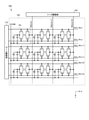
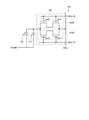
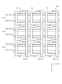
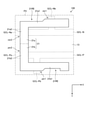
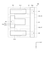
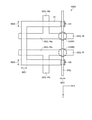
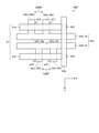
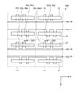
図1は、実施形態1に係る表示装置の構成例を示すブロック図である。図2は、実施形態1に係るTFT基板において、1画素の構成例を示す回路図である。実施形態1に係る表示装置200は、例えば、図示しない電子機器に搭載される。表示装置200は、電子機器の電源回路から電源電圧が印加され、電子機器のホストプロセッサである制御回路から出力される信号に基づいて画像表示を行う。表示装置200は、例えば電気泳動層160(後述の図15参照)を有する電気泳動型ディスプレイ(EPD)である。図1に示すように、表示装置200は、TFT基板100と、TFT基板100に接続するゲート駆動部110と、TFT基板100に接続するソース駆動部120と、を備える。
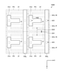
上記の実施形態1では、第1ゲート副線GCL-Nbと第2ゲート副線GCL―Pbは、X方向に互いに位置をずらして配置されていることを説明した。これにより、Y方向で隣り合う画素PX間において、第1ゲート副線GCL-Nbと第2ゲート副線GCL-Pbは互いに対向しないようにすることができることを説明した。しかしながら、本実施形態において、ゲート線GCLの配置はこれに限定されない。
上記の実施形態1では、半導体膜21を構成する第1部位21a及び第2部位21bが、平面視でL字状であることを説明した。しかしながら、本実施形態において、半導体膜21の形状はこれに限定されない。また、上記の実施形態1では、ゲート線GCLは、各画素PXにおいて、1本の第1ゲート副線GCL-Nbと、1本の第2ゲート副線GCL-Pbとを有することを説明した。しかしながら、本実施形態において、ゲート線GCLの構成はこれに限定されない。
上記の実施形態2では、第1ゲート副線GCL-Nb1と第2ゲート副線GCL―Pb1はX方向に互いに位置をずらして配置され、第1ゲート副線GCL-Nb2と第2ゲート副線GCL―Pb2もX方向に互いに位置をずらして配置されていることを説明した。しかしながら、本実施形態において、ゲート線GCLの配置は、これに限定されない。
上記の実施形態1、2では、ゲート線GCLが、X方向に延設されたゲート主線と、Y方向に延設されたゲート副線とを有することを説明した。しかしながら、本実施形態において、ゲート線GCLの構成はこれに限定されない。ゲート線GCLは、X方向に延設されたゲート主線のみで構成されていてもよい。
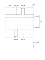
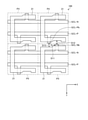
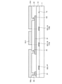
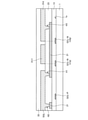
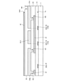
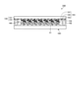
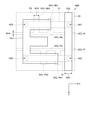
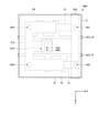
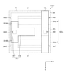
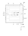
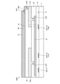
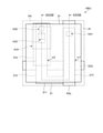
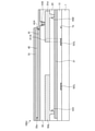
図28に示す平面図をXXIX-XXIX’線で切断した断面図である。図30は、実施形態3に係るTFT基板において、隣り合う画素間におけるゲート線と半導体膜との関係を示す平面図である。
上述の実施形態1から3では、画素トランジスタTRはCMOS(相補型MOS)構成であり、NMOSトランジスタNTR及びPMOSトランジスタPTRの両方を有することを説明した。しかしながら、本実施形態において、画素トランジスタTRはCMOS(相補型MOS)構成に限定されない。画素トランジスタTRは、NMOSトランジスタNTR及びPMOSトランジスタPTRのうち、どちらか一方のみを有する構成であってもよい。
13 絶縁膜
21 半導体膜
23 層間絶縁膜
31d ドレイン
31s ソース
31r、31r1、31r2 遮光膜
33 平坦化膜
41 共通電極
45 絶縁膜
51 画素電極
100、100A、100B、100C、100D、100E、100F、100G、100H、100J TFT基板
110 ゲート駆動部
120 ソース駆動部
130 対向基板
131 基材
133 対向電極
160 電気泳動層
200 表示装置
C1 第1保持容量
C2 第2保持容量
GCL ゲート線
NTR NMOSトランジスタ
ntr1 第1NMOSトランジスタ
ntr2 第2NMOSトランジスタ
PTR PMOSトランジスタ
ptr1 第1PMOSトランジスタ
ptr2 第2PMOSトランジスタ
PX 画素
TR 画素トランジスタ
VCOM 共通電位
Claims (8)
- 第1方向に延設される第1ゲート線と第2ゲート線と、
前記第1ゲート線及び前記第2ゲート線と平面視で交差する信号線と、
前記信号線に接続する半導体膜と、
前記半導体膜に接続するドレイン電極と、
前記信号線と前記ドレイン電極を覆う平坦化膜と、
前記ドレイン電極に接続する画素電極と、を備え、
前記半導体膜は、前記第1ゲート線に平行に延設される第1直線部と、前記第2ゲート線に平行に延設される第2直線部と、前記信号線に平行に延設される第3直線部と、を有し、
平面視において、前記第1ゲート線及び前記第2ゲート線は、前記第1直線部と前記第2直線部との間に位置し、
平面視において、前記ドレイン電極と前記画素電極を接続する前記平坦化膜の第1コンタクトホールは、前記第1ゲート線と前記第2ゲート線の間に位置し、
前記第3直線部は、前記第1直線部と前記第2直線部とを接続し、
前記第3直線部は、前記第1ゲート線及び前記第2ゲート線と交差し、
前記第3直線部は、前記信号線と重畳しない、TFT基板。 - 前記半導体膜と前記ドレイン電極との間に層間絶縁膜を有し、
前記層間絶縁膜の前記第3直線部と前記ドレイン電極とを接続する第2コンタクトホールは、平面視において前記第1ゲート線と前記第2ゲート線の間に位置する、請求項1に記載のTFT基板。 - 前記層間絶縁膜はさらに前記第1直線部と前記信号線を接続する第3コンタクトホールと、前記第2直線部と前記信号線を接続する第4コンタクトホールを備える、請求項2に記載のTFT基板。
- 前記半導体膜は前記信号線に平行に延設される第4直線部を更に有し、
前記第4直線部は前記第1直線部と前記第2直線部とを接続し、
前記信号線は前記層間絶縁膜に形成された第5コンタクトホールを介して前記第4直線部と接続され、
前記第5コンタクトホールは平面視において前記第1ゲート線と前記第2ゲート線との間にある、請求項2に記載のTFT基板。 - 第1ゲート線と、
前記第1ゲート線に平行な第2ゲート線と、
前記第1ゲート線及び前記第2ゲート線と平面視で交差する信号線と、
前記第1ゲート線及び前記第2ゲート線と平面視で交差し、前記信号線に接続する半導体膜と、を備え、
前記半導体膜は、前記第1ゲート線に平行な第1直線部と、前記第2ゲート線に平行な第2直線部と、前記信号線に平行な第3直線部と、を有し、前記第3直線部は前記第1直線部と前記第2直線部とを接続し、
前記第3直線部は、前記第1ゲート線及び前記第2ゲート線に交差し、前記信号線に重畳しない、TFT基板。 - 前記半導体膜はさらに前記信号線に平行な第4直線部と、を有し、
前記第4直線部は前記第1直線部と前記第2直線部とを接続し、
前記半導体膜の平面視による形状は環状である、請求項5に記載のTFT基板。 - 前記第4直線部は前記信号線に重畳し、前記第3直線部及び前記第4直線部はそれぞれ前記第1ゲート線及び前記第2ゲート線に交差する、請求項6に記載のTFT基板。
- 絶縁性の基材と、
前記基材の一方の面側に設けられる画素電極と、
前記基材と前記画素電極との間に設けられる画素トランジスタと、をさらに備え、
前記画素トランジスタは、
NMOSトランジスタと、
前記NMOSトランジスタに並列に接続するPMOSトランジスタと、を有し、
前記NMOSトランジスタのゲートは前記第1ゲート線に接続し、
前記NMOSトランジスタのソースは前記信号線に接続し、
前記NMOSトランジスタのドレインは前記画素電極に接続し、
前記PMOSトランジスタのゲートは前記第2ゲート線に接続し、
前記PMOSトランジスタのソースは前記信号線に接続し、
前記PMOSトランジスタのドレインは前記画素電極に接続している、請求項5から7のいずれか1項に記載のTFT基板。
Priority Applications (3)
| Application Number | Priority Date | Filing Date | Title |
|---|---|---|---|
| JP2018007271A JP6991865B2 (ja) | 2018-01-19 | 2018-01-19 | Tft基板 |
| PCT/JP2018/047970 WO2019142638A1 (ja) | 2018-01-19 | 2018-12-26 | Tft基板 |
| US16/930,744 US11171241B2 (en) | 2018-01-19 | 2020-07-16 | TFT substrate |
Applications Claiming Priority (1)
| Application Number | Priority Date | Filing Date | Title |
|---|---|---|---|
| JP2018007271A JP6991865B2 (ja) | 2018-01-19 | 2018-01-19 | Tft基板 |
Publications (2)
| Publication Number | Publication Date |
|---|---|
| JP2019124890A JP2019124890A (ja) | 2019-07-25 |
| JP6991865B2 true JP6991865B2 (ja) | 2022-01-13 |
Family
ID=67301439
Family Applications (1)
| Application Number | Title | Priority Date | Filing Date |
|---|---|---|---|
| JP2018007271A Active JP6991865B2 (ja) | 2018-01-19 | 2018-01-19 | Tft基板 |
Country Status (3)
| Country | Link |
|---|---|
| US (1) | US11171241B2 (ja) |
| JP (1) | JP6991865B2 (ja) |
| WO (1) | WO2019142638A1 (ja) |
Families Citing this family (3)
| Publication number | Priority date | Publication date | Assignee | Title |
|---|---|---|---|---|
| JP7529758B2 (ja) * | 2020-03-19 | 2024-08-06 | 京東方科技集團股▲ふん▼有限公司 | 表示基板及び表示装置 |
| JP7751416B2 (ja) * | 2021-08-23 | 2025-10-08 | 株式会社ジャパンディスプレイ | 検出装置 |
| CN118284984A (zh) * | 2021-11-22 | 2024-07-02 | 夏普显示科技株式会社 | 有源矩阵基板及液晶显示装置 |
Citations (3)
| Publication number | Priority date | Publication date | Assignee | Title |
|---|---|---|---|---|
| JP2004241700A (ja) | 2003-02-07 | 2004-08-26 | Seiko Epson Corp | 相補型薄膜トランジスタ回路、電気光学装置、電子機器 |
| JP2010085956A (ja) | 2008-10-03 | 2010-04-15 | Seiko Epson Corp | 電気光学装置、電子機器および投射型表示装置 |
| JP2010239108A (ja) | 2009-03-13 | 2010-10-21 | Seiko Epson Corp | 薄膜半導体装置、電気光学装置、および電子機器 |
Family Cites Families (2)
| Publication number | Priority date | Publication date | Assignee | Title |
|---|---|---|---|---|
| JPH02178632A (ja) * | 1988-12-29 | 1990-07-11 | Sony Corp | 液晶表示装置 |
| JP2011221125A (ja) | 2010-04-06 | 2011-11-04 | Seiko Epson Corp | 電気光学装置とその駆動方法、及び電子機器 |
-
2018
- 2018-01-19 JP JP2018007271A patent/JP6991865B2/ja active Active
- 2018-12-26 WO PCT/JP2018/047970 patent/WO2019142638A1/ja not_active Ceased
-
2020
- 2020-07-16 US US16/930,744 patent/US11171241B2/en active Active
Patent Citations (3)
| Publication number | Priority date | Publication date | Assignee | Title |
|---|---|---|---|---|
| JP2004241700A (ja) | 2003-02-07 | 2004-08-26 | Seiko Epson Corp | 相補型薄膜トランジスタ回路、電気光学装置、電子機器 |
| JP2010085956A (ja) | 2008-10-03 | 2010-04-15 | Seiko Epson Corp | 電気光学装置、電子機器および投射型表示装置 |
| JP2010239108A (ja) | 2009-03-13 | 2010-10-21 | Seiko Epson Corp | 薄膜半導体装置、電気光学装置、および電子機器 |
Also Published As
| Publication number | Publication date |
|---|---|
| JP2019124890A (ja) | 2019-07-25 |
| US20200350438A1 (en) | 2020-11-05 |
| US11171241B2 (en) | 2021-11-09 |
| WO2019142638A1 (ja) | 2019-07-25 |
Similar Documents
| Publication | Publication Date | Title |
|---|---|---|
| JP6999367B2 (ja) | 基板及び電気泳動装置 | |
| US9116407B2 (en) | Array substrate and manufacturing method thereof and display device | |
| JP5806383B2 (ja) | 液晶表示装置 | |
| JP6991865B2 (ja) | Tft基板 | |
| JP6690671B2 (ja) | 電気光学装置および電子機器 | |
| US11658188B2 (en) | Array substrate and display device | |
| CN115079472B (zh) | 电光装置和电子设备 | |
| JP7524745B2 (ja) | 電気光学装置および電子機器 | |
| JP6791283B2 (ja) | 電気光学装置、電子機器、および電気光学装置の製造方法 | |
| JP2021043244A (ja) | 電気光学装置および電子機器 | |
| JP6959359B2 (ja) | 基板及び電気泳動装置 | |
| JP7052844B2 (ja) | 電気光学装置および電子機器 | |
| JP2021092680A (ja) | 電気光学装置および電子機器 | |
| JP7810046B2 (ja) | 電気光学装置及び電子機器 | |
| CN115079473B (zh) | 电光装置和电子设备 | |
| JP6835122B2 (ja) | 電気光学装置および電子機器 | |
| JP7302398B2 (ja) | 電気光学装置および電子機器 | |
| JP2023147678A (ja) | 電気光学装置および電子機器 | |
| JP2025029950A (ja) | 電気光学装置および電子機器 | |
| JP2023147679A (ja) | 電気光学装置および電子機器 | |
| JP2023147695A (ja) | 電気光学装置及び電子機器 | |
| JP2022091911A (ja) | 電気光学装置および電子機器 | |
| JP2022112864A (ja) | 電気光学装置および電子機器 |
Legal Events
| Date | Code | Title | Description |
|---|---|---|---|
| A621 | Written request for application examination |
Free format text: JAPANESE INTERMEDIATE CODE: A621 Effective date: 20201125 |
|
| A131 | Notification of reasons for refusal |
Free format text: JAPANESE INTERMEDIATE CODE: A131 Effective date: 20210720 |
|
| A521 | Request for written amendment filed |
Free format text: JAPANESE INTERMEDIATE CODE: A523 Effective date: 20210917 |
|
| TRDD | Decision of grant or rejection written | ||
| A01 | Written decision to grant a patent or to grant a registration (utility model) |
Free format text: JAPANESE INTERMEDIATE CODE: A01 Effective date: 20211116 |
|
| A61 | First payment of annual fees (during grant procedure) |
Free format text: JAPANESE INTERMEDIATE CODE: A61 Effective date: 20211208 |
|
| R150 | Certificate of patent or registration of utility model |
Ref document number: 6991865 Country of ref document: JP Free format text: JAPANESE INTERMEDIATE CODE: R150 |
|
| R250 | Receipt of annual fees |
Free format text: JAPANESE INTERMEDIATE CODE: R250 |
|
| S111 | Request for change of ownership or part of ownership |
Free format text: JAPANESE INTERMEDIATE CODE: R313113 |
|
| R350 | Written notification of registration of transfer |
Free format text: JAPANESE INTERMEDIATE CODE: R350 |
|
| R250 | Receipt of annual fees |
Free format text: JAPANESE INTERMEDIATE CODE: R250 |