JP6991865B2 - TFT substrate - Google Patents
TFT substrate Download PDFInfo
- Publication number
- JP6991865B2 JP6991865B2 JP2018007271A JP2018007271A JP6991865B2 JP 6991865 B2 JP6991865 B2 JP 6991865B2 JP 2018007271 A JP2018007271 A JP 2018007271A JP 2018007271 A JP2018007271 A JP 2018007271A JP 6991865 B2 JP6991865 B2 JP 6991865B2
- Authority
- JP
- Japan
- Prior art keywords
- gate
- line
- gcl
- tft substrate
- transistor
- Prior art date
- Legal status (The legal status is an assumption and is not a legal conclusion. Google has not performed a legal analysis and makes no representation as to the accuracy of the status listed.)
- Active
Links
Images


Classifications
-
- H—ELECTRICITY
- H10—SEMICONDUCTOR DEVICES; ELECTRIC SOLID-STATE DEVICES NOT OTHERWISE PROVIDED FOR
- H10D—INORGANIC ELECTRIC SEMICONDUCTOR DEVICES
- H10D86/00—Integrated devices formed in or on insulating or conducting substrates, e.g. formed in silicon-on-insulator [SOI] substrates or on stainless steel or glass substrates
- H10D86/40—Integrated devices formed in or on insulating or conducting substrates, e.g. formed in silicon-on-insulator [SOI] substrates or on stainless steel or glass substrates characterised by multiple TFTs
- H10D86/421—Integrated devices formed in or on insulating or conducting substrates, e.g. formed in silicon-on-insulator [SOI] substrates or on stainless steel or glass substrates characterised by multiple TFTs having a particular composition, shape or crystalline structure of the active layer
-
- H—ELECTRICITY
- H10—SEMICONDUCTOR DEVICES; ELECTRIC SOLID-STATE DEVICES NOT OTHERWISE PROVIDED FOR
- H10D—INORGANIC ELECTRIC SEMICONDUCTOR DEVICES
- H10D30/00—Field-effect transistors [FET]
- H10D30/60—Insulated-gate field-effect transistors [IGFET]
- H10D30/67—Thin-film transistors [TFT]
- H10D30/6704—Thin-film transistors [TFT] having supplementary regions or layers in the thin films or in the insulated bulk substrates for controlling properties of the device
- H10D30/6713—Thin-film transistors [TFT] having supplementary regions or layers in the thin films or in the insulated bulk substrates for controlling properties of the device characterised by the properties of the source or drain regions, e.g. compositions or sectional shapes
-
- G—PHYSICS
- G02—OPTICS
- G02F—OPTICAL DEVICES OR ARRANGEMENTS FOR THE CONTROL OF LIGHT BY MODIFICATION OF THE OPTICAL PROPERTIES OF THE MEDIA OF THE ELEMENTS INVOLVED THEREIN; NON-LINEAR OPTICS; FREQUENCY-CHANGING OF LIGHT; OPTICAL LOGIC ELEMENTS; OPTICAL ANALOGUE/DIGITAL CONVERTERS
- G02F1/00—Devices or arrangements for the control of the intensity, colour, phase, polarisation or direction of light arriving from an independent light source, e.g. switching, gating or modulating; Non-linear optics
- G02F1/01—Devices or arrangements for the control of the intensity, colour, phase, polarisation or direction of light arriving from an independent light source, e.g. switching, gating or modulating; Non-linear optics for the control of the intensity, phase, polarisation or colour
- G02F1/13—Devices or arrangements for the control of the intensity, colour, phase, polarisation or direction of light arriving from an independent light source, e.g. switching, gating or modulating; Non-linear optics for the control of the intensity, phase, polarisation or colour based on liquid crystals, e.g. single liquid crystal display cells
- G02F1/133—Constructional arrangements; Operation of liquid crystal cells; Circuit arrangements
- G02F1/136—Liquid crystal cells structurally associated with a semi-conducting layer or substrate, e.g. cells forming part of an integrated circuit
- G02F1/1362—Active matrix addressed cells
- G02F1/1368—Active matrix addressed cells in which the switching element is a three-electrode device
-
- G—PHYSICS
- G02—OPTICS
- G02F—OPTICAL DEVICES OR ARRANGEMENTS FOR THE CONTROL OF LIGHT BY MODIFICATION OF THE OPTICAL PROPERTIES OF THE MEDIA OF THE ELEMENTS INVOLVED THEREIN; NON-LINEAR OPTICS; FREQUENCY-CHANGING OF LIGHT; OPTICAL LOGIC ELEMENTS; OPTICAL ANALOGUE/DIGITAL CONVERTERS
- G02F1/00—Devices or arrangements for the control of the intensity, colour, phase, polarisation or direction of light arriving from an independent light source, e.g. switching, gating or modulating; Non-linear optics
- G02F1/01—Devices or arrangements for the control of the intensity, colour, phase, polarisation or direction of light arriving from an independent light source, e.g. switching, gating or modulating; Non-linear optics for the control of the intensity, phase, polarisation or colour
- G02F1/165—Devices or arrangements for the control of the intensity, colour, phase, polarisation or direction of light arriving from an independent light source, e.g. switching, gating or modulating; Non-linear optics for the control of the intensity, phase, polarisation or colour based on translational movement of particles in a fluid under the influence of an applied field
- G02F1/166—Devices or arrangements for the control of the intensity, colour, phase, polarisation or direction of light arriving from an independent light source, e.g. switching, gating or modulating; Non-linear optics for the control of the intensity, phase, polarisation or colour based on translational movement of particles in a fluid under the influence of an applied field characterised by the electro-optical or magneto-optical effect
- G02F1/167—Devices or arrangements for the control of the intensity, colour, phase, polarisation or direction of light arriving from an independent light source, e.g. switching, gating or modulating; Non-linear optics for the control of the intensity, phase, polarisation or colour based on translational movement of particles in a fluid under the influence of an applied field characterised by the electro-optical or magneto-optical effect by electrophoresis
-
- G—PHYSICS
- G09—EDUCATION; CRYPTOGRAPHY; DISPLAY; ADVERTISING; SEALS
- G09F—DISPLAYING; ADVERTISING; SIGNS; LABELS OR NAME-PLATES; SEALS
- G09F9/00—Indicating arrangements for variable information in which the information is built-up on a support by selection or combination of individual elements
- G09F9/30—Indicating arrangements for variable information in which the information is built-up on a support by selection or combination of individual elements in which the desired character or characters are formed by combining individual elements
-
- G—PHYSICS
- G09—EDUCATION; CRYPTOGRAPHY; DISPLAY; ADVERTISING; SEALS
- G09G—ARRANGEMENTS OR CIRCUITS FOR CONTROL OF INDICATING DEVICES USING STATIC MEANS TO PRESENT VARIABLE INFORMATION
- G09G3/00—Control arrangements or circuits, of interest only in connection with visual indicators other than cathode-ray tubes
- G09G3/20—Control arrangements or circuits, of interest only in connection with visual indicators other than cathode-ray tubes for presentation of an assembly of a number of characters, e.g. a page, by composing the assembly by combination of individual elements arranged in a matrix no fixed position being assigned to or needed to be assigned to the individual characters or partial characters
- G09G3/34—Control arrangements or circuits, of interest only in connection with visual indicators other than cathode-ray tubes for presentation of an assembly of a number of characters, e.g. a page, by composing the assembly by combination of individual elements arranged in a matrix no fixed position being assigned to or needed to be assigned to the individual characters or partial characters by control of light from an independent source
-
- H—ELECTRICITY
- H10—SEMICONDUCTOR DEVICES; ELECTRIC SOLID-STATE DEVICES NOT OTHERWISE PROVIDED FOR
- H10D—INORGANIC ELECTRIC SEMICONDUCTOR DEVICES
- H10D30/00—Field-effect transistors [FET]
- H10D30/60—Insulated-gate field-effect transistors [IGFET]
- H10D30/67—Thin-film transistors [TFT]
- H10D30/674—Thin-film transistors [TFT] characterised by the active materials
- H10D30/6755—Oxide semiconductors, e.g. zinc oxide, copper aluminium oxide or cadmium stannate
-
- H—ELECTRICITY
- H10—SEMICONDUCTOR DEVICES; ELECTRIC SOLID-STATE DEVICES NOT OTHERWISE PROVIDED FOR
- H10D—INORGANIC ELECTRIC SEMICONDUCTOR DEVICES
- H10D30/00—Field-effect transistors [FET]
- H10D30/60—Insulated-gate field-effect transistors [IGFET]
- H10D30/67—Thin-film transistors [TFT]
- H10D30/6757—Thin-film transistors [TFT] characterised by the structure of the channel, e.g. transverse or longitudinal shape or doping profile
-
- H—ELECTRICITY
- H10—SEMICONDUCTOR DEVICES; ELECTRIC SOLID-STATE DEVICES NOT OTHERWISE PROVIDED FOR
- H10D—INORGANIC ELECTRIC SEMICONDUCTOR DEVICES
- H10D86/00—Integrated devices formed in or on insulating or conducting substrates, e.g. formed in silicon-on-insulator [SOI] substrates or on stainless steel or glass substrates
- H10D86/40—Integrated devices formed in or on insulating or conducting substrates, e.g. formed in silicon-on-insulator [SOI] substrates or on stainless steel or glass substrates characterised by multiple TFTs
- H10D86/441—Interconnections, e.g. scanning lines
-
- H—ELECTRICITY
- H10—SEMICONDUCTOR DEVICES; ELECTRIC SOLID-STATE DEVICES NOT OTHERWISE PROVIDED FOR
- H10D—INORGANIC ELECTRIC SEMICONDUCTOR DEVICES
- H10D86/00—Integrated devices formed in or on insulating or conducting substrates, e.g. formed in silicon-on-insulator [SOI] substrates or on stainless steel or glass substrates
- H10D86/40—Integrated devices formed in or on insulating or conducting substrates, e.g. formed in silicon-on-insulator [SOI] substrates or on stainless steel or glass substrates characterised by multiple TFTs
- H10D86/451—Integrated devices formed in or on insulating or conducting substrates, e.g. formed in silicon-on-insulator [SOI] substrates or on stainless steel or glass substrates characterised by multiple TFTs characterised by the compositions or shapes of the interlayer dielectrics
-
- H—ELECTRICITY
- H10—SEMICONDUCTOR DEVICES; ELECTRIC SOLID-STATE DEVICES NOT OTHERWISE PROVIDED FOR
- H10D—INORGANIC ELECTRIC SEMICONDUCTOR DEVICES
- H10D86/00—Integrated devices formed in or on insulating or conducting substrates, e.g. formed in silicon-on-insulator [SOI] substrates or on stainless steel or glass substrates
- H10D86/40—Integrated devices formed in or on insulating or conducting substrates, e.g. formed in silicon-on-insulator [SOI] substrates or on stainless steel or glass substrates characterised by multiple TFTs
- H10D86/60—Integrated devices formed in or on insulating or conducting substrates, e.g. formed in silicon-on-insulator [SOI] substrates or on stainless steel or glass substrates characterised by multiple TFTs wherein the TFTs are in active matrices
-
- H—ELECTRICITY
- H10—SEMICONDUCTOR DEVICES; ELECTRIC SOLID-STATE DEVICES NOT OTHERWISE PROVIDED FOR
- H10D—INORGANIC ELECTRIC SEMICONDUCTOR DEVICES
- H10D86/00—Integrated devices formed in or on insulating or conducting substrates, e.g. formed in silicon-on-insulator [SOI] substrates or on stainless steel or glass substrates
- H10D86/40—Integrated devices formed in or on insulating or conducting substrates, e.g. formed in silicon-on-insulator [SOI] substrates or on stainless steel or glass substrates characterised by multiple TFTs
- H10D86/421—Integrated devices formed in or on insulating or conducting substrates, e.g. formed in silicon-on-insulator [SOI] substrates or on stainless steel or glass substrates characterised by multiple TFTs having a particular composition, shape or crystalline structure of the active layer
- H10D86/423—Integrated devices formed in or on insulating or conducting substrates, e.g. formed in silicon-on-insulator [SOI] substrates or on stainless steel or glass substrates characterised by multiple TFTs having a particular composition, shape or crystalline structure of the active layer comprising semiconductor materials not belonging to the Group IV, e.g. InGaZnO
Landscapes
- Physics & Mathematics (AREA)
- Engineering & Computer Science (AREA)
- General Physics & Mathematics (AREA)
- Nonlinear Science (AREA)
- Theoretical Computer Science (AREA)
- Computer Hardware Design (AREA)
- Optics & Photonics (AREA)
- Chemical & Material Sciences (AREA)
- Microelectronics & Electronic Packaging (AREA)
- Molecular Biology (AREA)
- Life Sciences & Earth Sciences (AREA)
- Electrochemistry (AREA)
- Chemical Kinetics & Catalysis (AREA)
- Mathematical Physics (AREA)
- Crystallography & Structural Chemistry (AREA)
- Health & Medical Sciences (AREA)
- Liquid Crystal (AREA)
- Thin Film Transistor (AREA)
- Devices For Indicating Variable Information By Combining Individual Elements (AREA)
- Electrochromic Elements, Electrophoresis, Or Variable Reflection Or Absorption Elements (AREA)
- Control Of Indicators Other Than Cathode Ray Tubes (AREA)
Description
本発明は、TFT(Thin Film Transistor)基板に関する。 The present invention relates to a TFT (Thin Film Transistor) substrate.
近年、携帯電話及び電子ペーパー等のモバイル電子機器向け等の表示装置の需要が高くなっている。例えば、電子ペーパーで用いられる電気泳動型ディスプレイ(Electrophoretic Display:EPD)では、画像の書き換え時の電位を保持するメモリ性を有している。EPDは、フレーム毎に1回書き換えを行えば、次のフレームにおいて書き換えが行われるまで書き換え時の電位が保持される。このため、EPDは、低消費電力駆動が可能である。例えば、EPDの画素トランジスタを、PチャネルトランジスタとNチャネルトランジスタとを組み合わせたCMOS(相補型MOS)構成とすることで、低消費電力化を図る技術が開示されている(例えば、特許文献1)。 In recent years, there has been an increasing demand for display devices for mobile electronic devices such as mobile phones and electronic paper. For example, an electrophoretic display (EPD) used in electronic paper has a memory property of holding a potential at the time of rewriting an image. If the EPD is rewritten once for each frame, the potential at the time of rewriting is maintained until the rewriting is performed in the next frame. Therefore, the EPD can be driven with low power consumption. For example, a technique for reducing power consumption is disclosed by forming an EPD pixel transistor into a CMOS (complementary MOS) configuration in which a P-channel transistor and an N-channel transistor are combined (for example, Patent Document 1). ..
屋外のような強い光が当たる環境下では、表示面に入射する光が画素トランジスタに届く可能性がある。画素トランジスタに強い光が入射すると、光伝導効果によって光リーク電流が発生し、画素トランジスタが誤作動する可能性がある。 In an environment exposed to strong light such as outdoors, the light incident on the display surface may reach the pixel transistor. When strong light is incident on the pixel transistor, a light leakage current is generated due to the photoconducting effect, and the pixel transistor may malfunction.
本発明は、上記に鑑みてなされたものであり、信頼性を向上できるようにしたTFT基板を提供することを目的とする。 The present invention has been made in view of the above, and an object of the present invention is to provide a TFT substrate capable of improving reliability.
一態様に係るTFT基板は、第1方向に延設される第1ゲート線と第2ゲート線と、前記第1ゲート線及び前記第2ゲート線と平面視で交差する信号線と、前記信号線に接続する半導体膜と、前記半導体膜に接続するドレイン電極と、前記信号線と前記ドレイン電極を覆う平坦化膜と、前記ドレイン電極に接続する画素電極と、を備え、前記半導体膜は、前記第1ゲート線に平行に延設される第1直線部と、前記第2ゲート線に平行に延設される第2直線部と、を有し、平面視において、前記第1ゲート線及び前記第2ゲート線は、前記第1直線部と前記第2直線部との間に位置し、平面視において、前記ドレイン電極と前記画素電極を接続する前記平坦化膜の第1コンタクトホールは、前記第1ゲート線と前記第2ゲート線の間に位置する。 The TFT substrate according to one embodiment includes a first gate line and a second gate line extending in the first direction, a signal line intersecting the first gate line and the second gate line in a plan view, and the signal. The semiconductor film comprises a semiconductor film connected to a wire, a drain electrode connected to the semiconductor film, a flattening film covering the signal line and the drain electrode, and a pixel electrode connected to the drain electrode. It has a first straight line portion extending parallel to the first gate line and a second straight line portion extending parallel to the second gate line, and has the first gate line and the first straight line portion in a plan view. The second gate line is located between the first straight line portion and the second straight line portion, and in a plan view, the first contact hole of the flattening film connecting the drain electrode and the pixel electrode is a first contact hole. It is located between the first gate line and the second gate line.
別の態様に係るTFT基板は、第1ゲート線と、前記第1ゲート線に平行な第2ゲート線と、前記第1ゲート線及び前記第2ゲート線と平面視で交差する信号線と、前記第1ゲート線及び前記第2ゲート線と平面視で交差し、前記信号線に接続する半導体膜と、を備え、前記半導体膜は、第1ゲート線に平行な第1直線部と、前記第2ゲート線に平行な第2直線部と、前記信号線に平行な第3直線部と、を有し、前記第3直線部は前記第1直線部と前記第2直線部とを接続する。 The TFT substrate according to another aspect includes a first gate line, a second gate line parallel to the first gate line, and a signal line intersecting the first gate line and the second gate line in a plan view. A semiconductor film that intersects the first gate line and the second gate line in a plan view and is connected to the signal line is provided, and the semiconductor film has a first straight line portion parallel to the first gate line and the above. It has a second straight line portion parallel to the second gate line and a third straight line portion parallel to the signal line, and the third straight line portion connects the first straight line portion and the second straight line portion. ..
本発明を実施するための形態(実施形態)につき、図面を参照しつつ詳細に説明する。以下の実施形態に記載した内容により本発明が限定されるものではない。また、以下に記載した構成要素には、当業者が容易に想定できるもの、実質的に同一のものが含まれる。さらに、以下に記載した構成要素は適宜組み合わせることが可能である。なお、開示はあくまで一例にすぎず、当業者において、発明の主旨を保っての適宜変更について容易に想到し得るものについては、当然に本発明の範囲に含有されるものである。また、図面は説明をより明確にするため、実際の態様に比べ、各部の幅、厚さ、形状等について模式的に表される場合があるが、あくまで一例であって、本発明の解釈を限定するものではない。また、本明細書と各図において、既出の図に関して前述したものと同様の要素には、同一の符号を付して、詳細な説明を適宜省略することがある。 An embodiment (embodiment) for carrying out the present invention will be described in detail with reference to the drawings. The present invention is not limited to the contents described in the following embodiments. In addition, the components described below include those that can be easily assumed by those skilled in the art and those that are substantially the same. Furthermore, the components described below can be combined as appropriate. It should be noted that the disclosure is merely an example, and those skilled in the art can easily conceive of appropriate changes while maintaining the gist of the invention, which are naturally included in the scope of the present invention. Further, in order to clarify the explanation, the drawings may schematically represent the width, thickness, shape, etc. of each part as compared with the actual embodiment, but this is just an example, and the interpretation of the present invention is used. It is not limited. Further, in the present specification and each figure, the same elements as those described above with respect to the above-mentioned figures may be designated by the same reference numerals, and detailed description thereof may be omitted as appropriate.
また、本明細書では、図3における左右方向をX方向で示し、図3における上下方向をY方向で示す。X方向及びY方向は、基材1の一方の面1a(後述の図9参照)に平行である。平行については概ね平行に形成されるものであり、製造に伴う微妙なずれについては許容されるものとしている。
Further, in the present specification, the left-right direction in FIG. 3 is shown in the X direction, and the up-down direction in FIG. 3 is shown in the Y direction. The X and Y directions are parallel to one
(実施形態1)
図1は、実施形態1に係る表示装置の構成例を示すブロック図である。図2は、実施形態1に係るTFT基板において、1画素の構成例を示す回路図である。実施形態1に係る表示装置200は、例えば、図示しない電子機器に搭載される。表示装置200は、電子機器の電源回路から電源電圧が印加され、電子機器のホストプロセッサである制御回路から出力される信号に基づいて画像表示を行う。表示装置200は、例えば電気泳動層160(後述の図15参照)を有する電気泳動型ディスプレイ(EPD)である。図1に示すように、表示装置200は、TFT基板100と、TFT基板100に接続するゲート駆動部110と、TFT基板100に接続するソース駆動部120と、を備える。
(Embodiment 1)
FIG. 1 is a block diagram showing a configuration example of a display device according to the first embodiment. FIG. 2 is a circuit diagram showing a configuration example of one pixel in the TFT substrate according to the first embodiment. The
図1に示すように、TFT基板100は、複数の画素PXと、複数の第1ゲート線GCL-N(n)、GCL-N(n+1)、GCL-N(n+2)…と、複数の第2ゲート線GCL-P(n)、GCL-P(n+1)、GCL-P(n+2)…と、複数の信号線SGL(m)、SGL(m+1)、SGL(m+2)…と、を備える。n、mは、それぞれ1以上の整数である。以下の説明では、複数の第1ゲート線GCL-N(n)、GCL-N(n+1)、GCL-N(n+2)…を互いに区別して説明する必要がないときは、それぞれを第1ゲート線GCL-Nという。同様に、複数の第2ゲート線GCL-P(n)、GCL-P(n+1)、GCL-P(n+2)…を互いに区別して説明する必要がないときは、それぞれを第2ゲート線GCL-Pという。複数の信号線SGL(m)、SGL(m+1)、SGL(m+2)…を互いに区別して説明する必要がないときは、それぞれを信号線SGLという。
As shown in FIG. 1, the
複数の画素PXは、X方向と、X方向と交差するY方向とにそれぞれ並んでおり、2次元のマトリクス状に配置されている。複数の第1ゲート線GCL-Nは、X方向に延設されており、Y方向に並んでいる。複数の第2ゲート線GCL-Pも、X方向に延設されており、Y方向に並んでいる。Y方向において、第1ゲート線GCL-Nと第2ゲート線GCL-Pは交互に並んでいる。例えば、Y方向において、第1ゲート線GCL-N及び第2ゲート線GCL-Pは、第1ゲート線GCL-N(n)、第2ゲート線GCL-P(n)、第1ゲート線GCL-N(n+1)、第2ゲート線GCL-P(n+1)…の順で並んでいる。複数の信号線SGLは、Y方向に延設されており、X方向に並んでいる。これにより、複数の信号線SGLは、第1ゲート線GCL-N及び第2ゲート線GCL-Pと、平面視でそれぞれ直交している。なお、平面視とは、TFT基板100の基材1の一方の面1a(後述の図9参照)の法線方向から見ることを意味する。
The plurality of pixels PX are arranged in the X direction and in the Y direction intersecting the X direction, respectively, and are arranged in a two-dimensional matrix. The plurality of first gate lines GCL-N extend in the X direction and are arranged in the Y direction. A plurality of second gate lines GCL-P are also extended in the X direction and are arranged in the Y direction. In the Y direction, the first gate line GCL-N and the second gate line GCL-P are arranged alternately. For example, in the Y direction, the first gate line GCL-N and the second gate line GCL-P are the first gate line GCL-N (n), the second gate line GCL-P (n), and the first gate line GCL. -N (n + 1), the second gate line GCL-P (n + 1) ... Are arranged in this order. The plurality of signal lines SGL extend in the Y direction and are arranged in the X direction. As a result, the plurality of signal lines SGL are orthogonal to the first gate line GCL-N and the second gate line GCL-P, respectively, in a plan view. In addition, the plan view means that it is viewed from the normal direction of one
複数の第1ゲート線GCL-N及び複数の第2ゲート線GCL-Pは、ゲート駆動部110にそれぞれ接続している。複数の信号線SGLは、ソース駆動部120にそれぞれ接続している。
The plurality of first gate lines GCL-N and the plurality of second gate lines GCL-P are connected to the
ゲート駆動部110は、上述の制御回路から出力される信号に基づいて、第1ゲート駆動信号と、第2ゲート駆動信号とを生成する。ゲート駆動部110は、第1ゲート駆動信号を第1ゲート線GCL-Nに供給し、第2ゲート駆動信号を第2ゲート線GCL-Pに供給する。ソース駆動部120は、上述の制御回路から出力される信号に基づいて、ソース駆動信号を生成する。ソース駆動部120は、ソース駆動信号を信号線SGLに供給する。
The
ゲート駆動部110及びソース駆動部120はTFT基板100に設けられていてもよいし、対向基板130(後述の図15参照)に設けられていてもよい。また、ゲート駆動部110及びソース駆動部120は、TFT基板100に接続する他の回路基板(例えば、フレキシブル基板)に実装されたIC(Integrated Circuit)に搭載されていてもよい。
The
図2に示すように、TFT基板100の各画素PXは、画素トランジスタTRを備える。例えば、画素トランジスタTRはCMOS(相補型MOS)構成であり、NMOSトランジスタNTRと、PMOSトランジスタPTRとを有する。例えば、NMOSトランジスタNTRと、PMOSトランジスタPTRは、それぞれボトムゲート型である。
As shown in FIG. 2, each pixel PX of the
NMOSトランジスタNTRと、PMOSトランジスタPTRは並列に接続されている。NMOSトランジスタNTRのソースとPMOSトランジスタPTRのソースとが、信号線SGLに接続されている。また、NMOSトランジスタNTRのドレインとPMOSトランジスタPTRのドレインとが接続されている。実施形態1では、NMOSトランジスタNTRのソース及びPMOSトランジスタPTRのソースは、共通のソース31s(後述の図9参照)で構成されている。NMOSトランジスタNTRのドレイン及びPMOSトランジスタPTRのドレインは、共通のドレイン31d(後述の図6参照)で構成されている。
The MIMO transistor NTR and the polyclonal transistor PTR are connected in parallel. The source of the IGMP transistor NTR and the source of the polyclonal transistor PTR are connected to the signal line SGL. Further, the drain of the MIMO transistor NTR and the drain of the polyclonal transistor PTR are connected to each other. In the first embodiment, the source of the MIMO transistor NTR and the source of the polyclonal transistor PTR are composed of a
NMOSトランジスタNTRは、第1NMOSトランジスタntr1と、第2NMOSトランジスタntr2と、を有する。第1NMOSトランジスタntr1と第2NMOSトランジスタntr2は直列に接続されている。また、PMOSトランジスタPTRは、第1PMOSトランジスタptr1と、第2PMOSトランジスタptr2と、を有する。第1PMOSトランジスタptr1と第2PMOSトランジスタptr2は直列に接続されている。 The µtransistor NTR includes a first µtransistor ntr1 and a second NMOS transistor ntr2. The first µtransistor ntr1 and the second CAUTIONtransistor ntr2 are connected in series. Further, the polyclonal transistor PTR has a first polyclonal transistor ptr1 and a second polyclonal transistor ptr2. The first polyclonal transistor ptr1 and the second polyclonal transistor ptr2 are connected in series.
NMOSトランジスタNTRのゲートは、第1NMOSトランジスタntr1のゲートn1g(後述の図9参照)及び第2NMOSトランジスタntr2のゲートn2g(後述の図9参照)を有する。NMOSトランジスタNTRのゲートは、第1ゲート線GCL-Nに接続している。NMOSトランジスタNTRのソースは、信号線SGLに接続している。NMOSトランジスタNTRのドレインは、画素電極51(後述の図9参照)に接続している。NMOSトランジスタNTRのソースには、信号線SGLからソース駆動信号(映像信号)が供給される。NMOSトランジスタNTRのゲートには、第1ゲート線GCL-Nから第1ゲート駆動信号が供給される。NMOSトランジスタNTRに供給される第1ゲート駆動信号の電圧が所定の値以上になると、NMOSトランジスタNTRがオンする。これにより、信号線SGLからNMOSトランジスタNTRを介して、画素電極51にソース駆動信号(映像信号)が供給される。
The gate of the N The gate of the MIMO transistor NTR is connected to the first gate line GCL-N. The source of the µtransistor NTR is connected to the signal line SGL. The drain of the MIMO transistor NTR is connected to the pixel electrode 51 (see FIG. 9 described later). A source drive signal (video signal) is supplied from the signal line SGL to the source of the IGMP transistor NTR. A first gate drive signal is supplied from the first gate line GCL-N to the gate of the IGMP transistor NTR. When the voltage of the first gate drive signal supplied to the nanotube transistor NTR becomes equal to or higher than a predetermined value, the nanotube transistor NTR is turned on. As a result, the source drive signal (video signal) is supplied from the signal line SGL to the
PMOSトランジスタPTRのゲートは、第1PMOSトランジスタptr1のゲート及び第2PMOSトランジスタptr2のゲートを有する。PMOSトランジスタPTRのゲートは、第2ゲート線GCL-Pに接続している。PMOSトランジスタPTRのソースは、信号線SGLに接続している。PMOSトランジスタPTRのドレインは、画素電極51に接続している。PMOSトランジスタPTRのソースには、信号線SGLからソース駆動信号(映像信号)が供給される。PMOSトランジスタPTRのゲートには、第2ゲート線GCL-Pから第2ゲート駆動信号が供給される。PMOSトランジスタPTRに供給される第2ゲート駆動信号の電圧が所定の値以下になると、PMOSトランジスタPTRがオンする。これにより、信号線SGLからPMOSトランジスタPTRを介して、画素電極51にソース駆動信号(映像信号)が供給される。
The gate of the epitaxial transistor PTR has a gate of the first polyclonal transistor ptr1 and a gate of the second polyclonal transistor ptr2. The gate of the polyclonal transistor PTR is connected to the second gate line GCL-P. The source of the polyclonal transistor PTR is connected to the signal line SGL. The drain of the polyclonal transistor PTR is connected to the
また、TFT基板100の各画素PXは、第1保持容量C1と、第2保持容量C2とを有する。第1保持容量C1は、画素電極51と共通電極41(後述の図9参照)との間に形成される。第2保持容量C2は、対向基板130の対向電極133(後述の図15参照)と、画素電極51との間に形成される。画素電極51には、信号線SGLから画素トランジスタTRを介して、ソース駆動信号(映像信号)が供給される。また、共通電極41と対向電極133には、共通電位VCOMが供給される。画素電極51に供給されたソース駆動信号(映像信号)の電位は、第1保持容量C1と、第2保持容量C2とによって保持される。
Further, each pixel PX of the
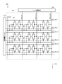
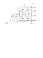
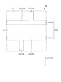
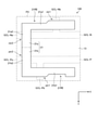
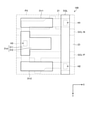
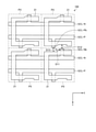
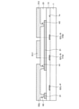
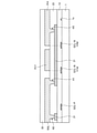
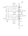
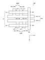
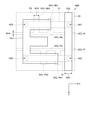
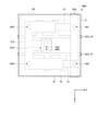
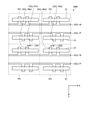
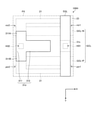
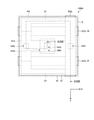
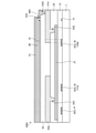
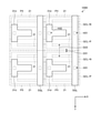
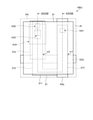
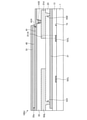
次に、TFT基板の構造について説明する。図3は、実施形態1に係るTFT基板において、複数の画素の配置例を示す平面図である。図4は、実施形態1に係るTFT基板の1画素において、ゲート線の構成例を示す平面図である。図5は、実施形態1に係るTFT基板の1画素において、半導体膜の構成例を示す平面図である。図5では、絶縁膜13で覆われている部位を破線で示している。図6は、実施形態1に係るTFT基板の1画素において、信号線、ドレイン及び遮光膜の構成例を示す平面図である。図6では、層間絶縁膜23で覆われている部位を破線で示している。図7は、TFT基板の1画素において、共通電極の構成例を示す平面図である。図8は、実施形態1に係るTFT基板の1画素の構成例を示す平面図である。図8では、画素電極51で覆われている部位を破線で示している。また、図8では、図面の複雑化を回避するために、図9に示す平坦化膜33、層間絶縁膜23及び絶縁膜13の図示を省略している。図9は、図8に示す平面図をIX-IX’線で切断した断面図である。
Next, the structure of the TFT substrate will be described. FIG. 3 is a plan view showing an arrangement example of a plurality of pixels in the TFT substrate according to the first embodiment. FIG. 4 is a plan view showing a configuration example of a gate line in one pixel of the TFT substrate according to the first embodiment. FIG. 5 is a plan view showing a configuration example of a semiconductor film in one pixel of the TFT substrate according to the first embodiment. In FIG. 5, the portion covered with the insulating
図3、図4及び図9に示すように、TFT基板100は、基材1と、基材1の一方の面1a上に設けられたゲート線GCLと、基材1の一方の面1a上に設けられた絶縁膜13とを有する。ゲート線GCLは、第1ゲート線GCL-Nと、第1ゲート線GCL-NとY方向で隣り合う第2ゲート線GCL-Pと、を有する。絶縁膜13は、第1ゲート線GCL-N及び第2ゲート線GCL-Pを覆っている。なお、絶縁膜13において、第1ゲート線GCL-N又は第2ゲート線GCL-Pと、半導体膜21とで挟まれる部位が、ゲート絶縁膜となる。
As shown in FIGS. 3, 4 and 9, the
図4に示すように、第1ゲート線GCL-Nは、第1ゲート主線GCL-Naと、第1ゲート主線GCL-Naに接続する第1ゲート副線GCL-Nbと、を有する。第1ゲート主線GCL-Naは、X方向に延設されている。第1ゲート主線GCL-Naは、複数の画素PX間で連続して設けられている。また、第1ゲート副線GCL-Nbは、第1ゲート主線GCL-NaからY方向に突き出ている。第1ゲート副線GCL-Nbの一端は第1ゲート主線GCL-Naに接続しているが、他端はどことも接続していない。第1ゲート副線GCL-Nbは、1つの画素PXに1つずつ設けられている。 As shown in FIG. 4, the first gate line GCL-N has a first gate main line GCL-Na and a first gate sub line GCL-Nb connected to the first gate main line GCL-Na. The first gate main line GCL-Na extends in the X direction. The first gate main line GCL-Na is continuously provided between a plurality of pixels PX. Further, the first gate sub-line GCL-Nb protrudes from the first gate main line GCL-Na in the Y direction. One end of the first gate sub-line GCL-Nb is connected to the first gate main line GCL-Na, but the other end is not connected to anything. The first gate sub-line GCL-Nb is provided one by one in one pixel PX.
図4に示すように、第2ゲート線GCL-Pは、第2ゲート主線GCL-Paと、第2ゲート主線GCL-Paに接続する第2ゲート副線GCL-Pbと、を有する。第2ゲート主線GCL-Paは、X方向に延設されている。第2ゲート主線GCL-Paは、複数の画素PX間で連続して設けられている。また、第2ゲート副線GCL-Pbは、第2ゲート主線GCL-PaからY方向に突き出ている。第2ゲート副線GCL-Pbの一端は第2ゲート主線GCL-Paに接続しているが、他端はどことも接続していない。第2ゲート副線GCL-Pbは、1つの画素PXに1つずつ設けられている。 As shown in FIG. 4, the second gate line GCL-P has a second gate main line GCL-Pa and a second gate sub line GCL-Pb connected to the second gate main line GCL-Pa. The second gate main line GCL-Pa extends in the X direction. The second gate main line GCL-Pa is continuously provided between the plurality of pixels PX. Further, the second gate sub-line GCL-Pb protrudes from the second gate main line GCL-Pa in the Y direction. One end of the second gate sub-line GCL-Pb is connected to the second gate main line GCL-Pa, but the other end is not connected to anything. The second gate sub-line GCL-Pb is provided one by one in one pixel PX.
また、図3、図5及び図9に示すように、TFT基板100は、絶縁膜13上に設けられた半導体膜21と、絶縁膜13上に設けられた層間絶縁膜23とを有する。層間絶縁膜23は、半導体膜21を覆っている。層間絶縁膜23には、コンタクトホールH1、H2、H3が設けられている。コンタクトホールH1、H2、H3は、半導体膜21を底面とする貫通穴である。
Further, as shown in FIGS. 3, 5 and 9, the
図5に示すように、半導体膜21は、第1部位21aと、第1部位21aに接続する第2部位21bとを有する。第1部位21aは、第1ゲート主線GCL-Na及び第1ゲート副線GCL-Nbとそれぞれ平面視で交差している。第2部位21bは、第2ゲート主線GCL-Pa及び第2ゲート副線GCL-Pbとそれぞれ平面視で交差している。
As shown in FIG. 5, the
例えば、第1部位21aは、X方向に延設され、第1ゲート副線GCL-Nbと平面視で交差する直線部21a1と、Y方向に延設され、第1ゲート主線GCL-Naと平面視で交差する直線部21a2と、を有する。直線部21a1のX方向の端部と、直線部21a2のY方向の端部とが互いに接続している。直線部21a1と直線部21a2とが成す角度は約90°である。これにより、第1部位21aは、平面視でL字状となっている。
For example, the
また、第2部位21bは、X方向に延設され、第2ゲート副線GCL-Pbと平面視で交差する直線部21b1と、Y方向に延設され、第2ゲート主線GCL-Paと平面視で交差する直線部21b2と、を有する。直線部21b1のX方向の端部と、直線部21b2のY方向の端部とが互いに接続している。直線部21b1と直線部21b2とが成す角度は約90°である。これにより、第2部位21bは、平面視でL字状となっている。
Further, the
第1ゲート線GCL-Nにおいて、半導体膜21の第1部位21aと平面視で交差する部位が、NMOSトランジスタNTRのゲートである。例えば、第1ゲート副線GCL-Nbにおいて、第1部位21aの直線部21a1と平面視で交差する領域が、第1NMOSトランジスタntr1のゲートn1gである。また、第1ゲート主線GCL-Naにおいて、第1部位21aの直線部21a2と平面視で交差する領域が、第2NMOSトランジスタntr2のゲートn2gである。
In the first gate line GCL-N, the portion that intersects the
同様に、第2ゲート線GCL-Pにおいて、半導体膜21の第2部位21bと平面視で交差する部位が、PMOSトランジスタPTRのゲートである。例えば、第2ゲート副線GCL-Pbにおいて、第2部位21bの直線部21b1と平面視で交差する領域が、第1PMOSトランジスタptr1のゲートである。また、第2ゲート主線GCL-Paにおいて、第2部位21bの直線部21b2と平面視で交差する領域が、第2PMOSトランジスタptr2のゲートである。
Similarly, in the second gate line GCL-P, the portion that intersects the
図6に示すように、半導体膜21の第1部位21aは、コンタクトホールH1を介して信号線SGLに接続している。半導体膜21の第2部位21bは、コンタクトホールH2を介して信号線SGLに接続している。
As shown in FIG. 6, the
また、図6及び図9に示すように、TFT基板100は、信号線SGLと、画素トランジスタTR(図2参照)のソース31s及びドレイン31dと、遮光膜31r1、31r2と、を有する。信号線SGLと、ソース31s及びドレイン31dと、遮光膜31r1、31r2は、層間絶縁膜23上にそれぞれ設けられている。つまり、信号線SGLと、ソース31s及びドレイン31dと、遮光膜31r1、31r2は、同一の層に設けられている。
Further, as shown in FIGS. 6 and 9, the
信号線SGLにおいて、コンタクトホールH1を埋め込んでいる部位とその周辺部、及び、コンタクトホールH2を埋め込んでいる部位とその周辺部が、画素トランジスタTRのソース31sである。また、ドレイン31dは、信号線SGLから離れた位置に配置されており、コンタクトホールH3を埋め込んでいる。信号線SGLと、ソース31s及びドレイン31dと、遮光膜31r1、31r2は、例えば、同一組成の導電膜で構成されている。ソース31sをソース電極、ドレイン31dをドレイン電極ということもできる。
In the signal line SGL, the portion where the contact hole H1 is embedded and its peripheral portion, and the portion where the contact hole H2 is embedded and its peripheral portion are the
図6に示すように、遮光膜31r1、31r2の平面視による形状は、例えば、互いに同一の形状で、同一の大きさである。遮光膜31r1、31r2の平面視による形状は、例えば、矩形である。遮光膜31r1は、X方向に延設されており、平面視で半導体膜21と重なっている。また、図6及び図9に示すように、遮光膜31r1は、平面視で、第1NMOSトランジスタntr1(図5参照)のゲートn1gのドレイン側と重なっている。遮光膜31r2は、X方向に延設されており、平面視で半導体膜21と重なっている。遮光膜31r2は、平面視で、第1PMOSトランジスタptr1(図5参照)のゲートの全領域と重なっている。
As shown in FIG. 6, the shapes of the light-shielding films 31r1 and 31r2 in a plan view are, for example, the same shape and the same size. The shapes of the light-shielding films 31r1 and 31r2 in a plan view are, for example, rectangular. The light-shielding film 31r1 extends in the X direction and overlaps with the
図6に示すように、ドレイン31dの平面視による形状は、例えばT字状である。ドレイン31dは、Y方向に延設された直線部311と、X方向に延設された直線部312とを有する。直線部311のX方向の中心部に、直線部312のY方向の一端が接続している。直線部311と直線部312とが成す角度は約90°である。直線部311は、平面視で、第2NMOSトランジスタntr2(図5参照)のゲートn2gのドレイン側と、第2PMOSトランジスタptr2(図5参照)のゲートのドレイン側と、それぞれ重なっている。
As shown in FIG. 6, the shape of the
また、図9に示すように、TFT基板100は、層間絶縁膜23上に設けられた絶縁性の平坦化膜33を有する。平坦化膜33は、信号線SGLを覆っている。平坦化膜33の上面33aは平坦であり、基材1の一方の面1aに平行となっている。平坦化膜33には、コンタクトホールH4が設けられている。コンタクトホールH4は、画素トランジスタTR(図2参照)のドレイン31dを底面とする貫通穴である。
Further, as shown in FIG. 9, the
また、図9に示すように、TFT基板100は、平坦化膜33上に設けられた共通電極41と、共通電極41上に設けられた絶縁膜45と、を有する。図7に示すように、共通電極41には、1つの画素PXに1つの貫通穴41Hが設けられている。貫通穴41Hは、平面視で、平坦化膜33に設けられたコンタクトホールH4を囲んでいる。
Further, as shown in FIG. 9, the
絶縁膜45は、共通電極41を覆っている。絶縁膜45は、第1保持容量C1(図2参照)の誘電体である。絶縁膜45は、貫通穴41Hの各内側面を覆っている。また、絶縁膜45には、貫通穴45Hが設けられている。貫通穴45Hの底部にコンタクトホールH4が位置する。
The insulating
また、図8及び図9に示すように、TFT基板100は、絶縁膜45上に設けられた画素電極51を有する。画素電極51は、絶縁膜45を介して共通電極41を覆っている。また、画素電極51は、貫通穴45HとコンタクトホールH4とを埋め込んでいる。これにより、画素電極51は、画素トランジスタTRのドレイン31dと接続している。
Further, as shown in FIGS. 8 and 9, the
画素電極51の平面視による形状は、例えば矩形である。TFT基板100において、複数の画素電極51は、X方向と、X方向と交差するY方向とにそれぞれ並んでおり、2次元のマトリクス状に配置されている。
The shape of the
なお、本実施形態では、1つの画素電極51と平面視で重なる領域が、1つの画素PXとなっている。より詳細には、平面視で隣り合う画素電極51間にはスペースS(図8参照)がある。このスペースSを通り、且つ、隣り合う画素電極51から等距離にある中心線(図8では、1点鎖線で表記)が、各画素PXを画定している。この中心線は想像線であり、実際に目視される線ではない。
In this embodiment, one pixel PX is a region that overlaps with one
図10は、実施形態1に係るTFT基板において、隣り合う画素間におけるゲート線と半導体膜との関係を示す平面図である。図4及び図10に示すように、実施形態1に係るTFT基板100では、第1ゲート副線GCL-Nbと第2ゲート副線GCL―PbはX方向に互いに位置をずらして配置されている。これによれば、図10に示すように、Y方向で隣り合う画素PX間において、第1ゲート副線GCL-Nb及び第2ゲート副線GCL-Pbは互いに対向しないようにすることができる。TFT基板100は、Y方向で隣り合う画素PX間のスペースを広げなくても、一方の画素PXの第1ゲート副線GCL-Nbと他方の画素PXの第2ゲート副線GCL-Pbとの間のX方向の離隔距離D11を大きく確保することができる。これにより、TFT基板100は、Y方向で隣り合う画素PX間において、ゲート線GCL同士が互いに影響を及ぼし合うことを防ぐことができる。
FIG. 10 is a plan view showing the relationship between the gate line and the semiconductor film between adjacent pixels in the TFT substrate according to the first embodiment. As shown in FIGS. 4 and 10, in the
また、図10に示すように、TFT基板10は、X方向及びY方向に並ぶ複数の画素PXを備える。各画素PX内には、半導体膜21と、第1ゲート副線GCL-Nb及び第2ゲート副線GCL-Pbが配置されている。図5及び図10に示すように、半導体膜21は、平面視で画素PXの外側を向く凹部21REを有する。Y方向で隣り合う画素PX間において、一方の画素PXの凹部21REは、他方の画素PXの第1ゲート副線GCL-Nb又は第2ゲート副線GCL-Pbと向かい合っている。これによれば、図10に示すように、TFT基板100は、Y方向で隣り合う画素PX間において、画素PX間のスペースを広げなくても、半導体膜21と第1ゲート副線GCL-Nbとの間の距離D12や、半導体膜21と第2ゲート副線GCL-Pbとの間の距離D13を大きく確保することができる。これにより、TFT基板100は、Y方向で隣り合う画素PX間において、半導体膜21とゲート線GCLとが互いに影響を及ぼし合うことを防ぐことができる。
Further, as shown in FIG. 10, the TFT substrate 10 includes a plurality of pixels PX arranged in the X direction and the Y direction. A
次に、TFT基板100の各部を構成する材料を例示する。基材1は、ガラスや可撓性の樹脂基板で構成されている。第1ゲート線GCL-N及び第2ゲート線GCL-Pは、モリブデンを含む材料で構成されている。絶縁膜13は、シリコン酸化膜及びシリコン窒化膜で構成されている無機絶縁膜である。例えば、絶縁膜13は、基材1側からシリコン酸化膜、シリコン窒化膜がこの順で積層された積層構造の膜で構成されている。半導体膜21は、ポリシリコン膜で構成されている。また、半導体膜21はポリシリコン膜に限らずアモルファス膜や酸化物半導体膜で構成されるものであっても良い。層間絶縁膜23は、シリコン酸化膜及びシリコン窒化膜で構成されている無機絶縁膜である。例えば、層間絶縁膜23は、基材1側からシリコン酸化膜、シリコン窒化膜、シリコン酸化膜がこの順で積層された積層構造の膜で構成されている。
Next, the materials constituting each part of the
信号線SGL(ソース31sを含む)と、ドレイン31dと、遮光膜31r1、31r2は、チタン及びアルミニウムとで構成されている。例えば、信号線SGLと、ドレイン31dと、遮光膜31r1、31r2は、基材1側からチタン、アルミニウム、チタンがこの順で積層された積層構造の膜で構成されている。平坦化膜33は、アクリル樹脂で構成されている有機絶縁膜である。共通電極41は、透光性の導電膜であるITO(Indium Tin Oxide)で構成されている。絶縁膜45は、シリコン窒化膜で構成されている無機絶縁膜である。画素電極51は、ITOで構成されている。
The signal line SGL (including the
なお、上記材料はあくまで一例である。本実施形態では、上記以外の材料でTFT基板100の各部が構成されていてもよい。例えば、第1ゲート線GCL-N及び第2ゲート線GCL-Pは、アルミニウム、銅、銀、モリブデン又はこれらの合金膜で構成されていてもよい。信号線SGLと、ドレイン31dと、遮光膜31r1、31r2は、チタンとアルミニウムとの合金である、チタンアルミニウムで構成されていてもよい。
The above material is just an example. In the present embodiment, each part of the
次に、実施形態1に係るTFT基板100の製造方法を、断面図及び平面図を参照しながら説明する。図11から図14は、TFT基板の製造方法を説明するための断面図である。図11から図14は、図9に示した断面図に対応しており、この断面図における製造過程を順に示している。
Next, the method of manufacturing the
図11に示すように、まず、製造装置(図示せず)は、基材1上にモリブデン等の導電膜(図示せず)を形成する。導電膜の形成は、スパッタ法等により行われる。次に、製造装置は、フォトリソグラフィ技術及びドライエッチング技術により導電膜をパターニングして、第1ゲート線GCL-N及び第2ゲート線GCL-Pを形成する。例えば、製造装置は、導電膜の上にレジスト(図示せず)を形成する。レジストは、フォトリソグラフィによりパターニングされ、第1ゲート線GCL-N及び第2ゲート線GCL-Pが形成される領域を覆い、それ以外の領域を露出する形状に形成される。次に、製造装置は、レジストから露出する領域の導電膜を、ドライエッチング技術により除去する。これにより、導電膜から第1ゲート線GCL-N及び第2ゲート線GCL-Pが形成される。第1ゲート線GCL-N及び第2ゲート線GCL-Pの形成後、製造装置は、レジストを除去する。
As shown in FIG. 11, first, the manufacturing apparatus (not shown) forms a conductive film (not shown) such as molybdenum on the
次に、製造装置は、基材1上に絶縁膜13を形成する。絶縁膜13の形成は、CVD(Chemical Vapor Deposition)法等により行われる。これにより、第1ゲート線GCL-N及び第2ゲート線GCL-Pは絶縁膜13で覆われる。次に、製造装置は、絶縁膜13上に半導体膜をする。半導体膜の形成は、CVD法等により行われる。次に、製造装置は、半導体膜をフォトリソグラフィ技術及びドライエッチング技術によりパターニングする。これにより、製造装置は、図5に示した形状の半導体膜21を形成する。半導体膜21の形成後、製造装置は、レジストを除去する。
Next, the manufacturing apparatus forms the insulating
TFT基板100では、第1ゲート線GCL-Nにおいて、半導体膜21と平面視で重なる2つの部位のうち、一方が第1NMOSトランジスタntr1のゲートn1gとなり、他方が第2NMOSトランジスタntr2のゲートn2gとなる。また、第2ゲート線GCL-Pにおいて、半導体膜21と平面視で重なる2つの部位のうち、一方が第1PMOSトランジスタptr1のゲートとなり、他方が第2PMOSトランジスタptr2のゲートとなる。
In the
次に、図12に示すように、製造装置は、絶縁膜13上に層間絶縁膜23を形成する。層間絶縁膜23の形成は、CVD法等により行われる。これにより、半導体膜21は層間絶縁膜23で覆われる。
Next, as shown in FIG. 12, the manufacturing apparatus forms the
次に、製造装置は、層間絶縁膜23にコンタクトホールH1、H2、H3を形成する。例えば、製造装置は、層間絶縁膜23の上にレジスト(図示せず)を形成する。レジストは、フォトリソグラフィによりパターニングされ、コンタクトホールH1、H2、H3が形成される領域を露出し、それ以外の領域を覆う形状に形成される。次に、製造装置は、レジストから露出する領域の層間絶縁膜23をドライエッチング技術により除去する。これにより、層間絶縁膜23にコンタクトホールH1、H2、H3が形成される。コンタクトホールH1、H2、H3の形成後、製造装置は、レジストを除去する。
Next, the manufacturing apparatus forms contact holes H1, H2, and H3 in the
次に、製造装置は、層間絶縁膜23上に信号線SGL(図9に示したソース31sを含む)と、ドレイン31dと、遮光膜31r1、31r2(図6参照)とを形成する。例えば、製造装置は、層間絶縁膜23上に金属膜として、チタンを形成し、次にアルミニウムを形成し、次にチタンを形成する。金属膜の形成は、スパッタ法等により行われる。次に、製造装置は、金属膜をフォトリソグラフィ技術及びドライエッチング技術によりパターニングする。これにより、製造装置は、コンタクトホールH1とコンタクトホールH2とを通して半導体膜21に接続する信号線SGLと、コンタクトホールH3を通して半導体膜21に接続するドレイン31dと、遮光膜31r1、31r2とを形成する。その後、製造装置は、レジストを除去する。
Next, the manufacturing apparatus forms a signal line SGL (including the
次に、図13に示すように、製造装置は、層間絶縁膜23上に平坦化膜33を形成する。平坦化膜33は絶縁性であり、例えばアクリル樹脂などの有機材料である。平坦化膜33の形成は、スリットコート法もしくはスピンコート法等により行われる。これにより、信号線SGLと、ドレイン31dと、遮光膜31r1、31r2は、平坦化膜33で覆われる。平坦化膜33にアクリル樹脂などの有機材料を用いると、平坦化膜33の膜厚を厚くすることが可能となる。このため、共通電極41と信号線SGLとの間の寄生容量や、共通電極41とドレイン31dとの間の寄生容量を低減することが可能となる。
Next, as shown in FIG. 13, the manufacturing apparatus forms the flattening
次に、図14に示すように、製造装置は、平坦化膜33上に共通電極41を形成する。例えば、製造装置は、平坦化膜33上にITO等の導電膜を形成する。導電膜の形成は、スパッタリング法等により行われる。次に、製造装置は、導電膜をフォトリソグラフィ技術及びドライエッチング技術によりパターニングする。これにより、製造装置は、貫通穴41Hを有する共通電極41を形成する。共通電極41の形成後、製造装置は、レジストを除去する。
Next, as shown in FIG. 14, the manufacturing apparatus forms a
次に、製造装置は、平坦化膜33にコンタクトホールH4を形成する。例えば、製造装置は、平坦化膜33上にレジスト(図示せず)を形成する。レジストによって、共通電極41は覆われる。レジストは、フォトリソグラフィによりパターニングされ、コンタクトホールH4が形成される領域を露出し、それ以外の領域を覆う形状に形成される。コンタクトホールH4が形成される領域は、平面視で、貫通穴41Hの内側である。次に、製造装置は、レジストから露出する領域の平坦化膜33をドライエッチング技術により除去する。これにより、平坦化膜33にコンタクトホールH4が形成される。コンタクトホールH4の形成後、製造装置は、レジストを除去する。
Next, the manufacturing apparatus forms the contact hole H4 in the flattening
次に、製造装置は、基材1の上方に絶縁膜45(図9参照)を形成する。絶縁膜45の形成は、CVD法等により行われる。これにより、共通電極41は絶縁膜45で覆われる。また、コンタクトホールH4の内側面及び底部も絶縁膜45で覆われる。次に、製造装置は、絶縁膜45のうち、コンタクトホールH4の底部を覆っている部位を除去する。例えば、製造装置は、絶縁膜45上にレジスト(図示せず)を形成する。レジストは、フォトリソグラフィによりパターニングされ、コンタクトホールH4の底部と平面視で重なる領域を露出し、それ以外の領域を覆う形状に形成される。次に、製造装置は、レジストから露出する領域の絶縁膜45をドライエッチング技術により除去する。これにより、コンタクトホールH4の底部が絶縁膜45から露出する。その後、製造装置は、レジストを除去する。
Next, the manufacturing apparatus forms an insulating film 45 (see FIG. 9) above the
次に、製造装置は、絶縁膜45上に画素電極51(図9参照)を形成する。例えば、製造装置は、絶縁膜45上にITO等の導電膜を形成する。導電膜の形成は、スパッタリング法等により行われる。次に、製造装置は、導電膜をフォトリソグラフィ技術及びドライエッチング技術によりパターニングする。これにより、製造装置は、コンタクトホールH4を通してドレイン31dに接続する画素電極51を形成する。画素電極51の形成後、製造装置は、レジストを除去する。以上の工程を経て、実施形態1に係るTFT基板100が完成する。
Next, the manufacturing apparatus forms the pixel electrode 51 (see FIG. 9) on the insulating
次に、実施形態1に係る表示装置200の構造について説明する。図15は、実施形態1に係る表示装置200の構成例を示す断面図である。図15に示すように、実施形態1に係る表示装置200は、上述のTFT基板100と、TFT基板100と対向して配置された対向基板130と、TFT基板100と対向基板130との間に配置された電気泳動層160と、シール部152と、を備える。
Next, the structure of the
対向基板130は、基材131と、対向電極133とを有する。基材131は、透光性のガラス基板、透光性の樹脂基板又は透光性の樹脂フィルムである。対向電極133は、基材131において、TFT基板100と対向する面側に設けられている。対向電極133は、透光性の導電膜であるITOで構成されている。対向電極133と画素電極51は、電気泳動層160を挟んで対向している。
The facing
シール部152は、TFT基板100と対向基板130との間に設けられている。TFT基板100、対向基板130及びシール部152により囲まれた内部の空間に電気泳動層160が封止されている。シール部152には接続部材153が設けられている。対向電極133は、接続部材153を介して、TFT基板100の共通電極41と接続される。これにより、対向電極133に共通電位VCOMが供給される。
The
電気泳動層160は、複数のマイクロカプセル163を含む。マイクロカプセル163の内部には、複数の黒色微粒子161と、複数の白色微粒子162と、分散液165とが封入されている。複数の黒色微粒子161及び複数の白色微粒子162は、分散液165に分散されている。分散液165は、例えばシリコーンオイル等の、透光性の液体である。黒色微粒子161は、電気泳動粒子であり、例えば負に帯電したグラファイトが用いられる。白色微粒子162は、電気泳動粒子であり、例えば正に帯電した酸化チタン(TiO2)が用いられる。
The
画素電極51と対向電極133との間に電界が形成されることにより、黒色微粒子161と白色微粒子162との分散状態が変化する。黒色微粒子161と白色微粒子162の分散状態に応じて、電気泳動層160を透過する光の透過状態が変化する。これにより、表示面に画像が表示される。例えば、対向電極133に共通電位VCOM(例えば、0V)が供給され、画素電極51に負の電位が供給されると、負に帯電している黒色微粒子161は対向基板130側に移動し、正に帯電している白色微粒子162はTFT基板100側に移動する。これにより、対向基板130側からTFT基板100を見ると、画素電極51と平面視で重なる領域(画素)は、黒表示となる。
By forming an electric field between the
以上説明したように、実施形態1に係るTFT基板100は、X方向に延設されるゲート線GCLと、ゲート線GCLとは異なる層でY方向に延設され、ゲート線GCLと交差する信号線SGLと、ゲート線GCL及び信号線SGLとは異なる層に設けられ、ゲート線GCLと交差する半導体膜21と、ゲート線GCL及び半導体膜21とは異なる層に設けられ、ゲート線GCLと半導体膜21とが交差する領域の少なくとも一部を覆う遮光膜31r1、31r2及びドレイン31dと、を備える。これによれば、遮光膜31r1、31r2と、遮光膜31r1、31r2と同一組成の導電膜で構成されているドレイン31dは、これらよりも基材1側に位置する画素トランジスタTRのゲートを遮光することができる。
As described above, the
例えば、遮光膜31r1は、第1NMOSトランジスタntr1のゲートのドレイン側と重なる位置に配置されている。遮光膜31r2は、第1PMOSトランジスタptr1のゲートのドレイン側と重なる位置に配置されている。ドレイン31dは、第2NMOSトランジスタntr2のゲートのドレイン側と、第2PMOSトランジスタptr2のゲートのドレイン側とに重なる位置に配置されている。これにより、画素トランジスタTRのゲートのドレイン側は遮光されている。
For example, the light-shielding film 31r1 is arranged at a position overlapping the drain side of the gate of the first µ transistor ntr1. The light-shielding film 31r2 is arranged at a position overlapping the drain side of the gate of the first polyclonal transistor ptr1. The
屋外のような強い光が当たる環境下では、EPDの表示面に入射する光が電気泳動層を透過して、画素トランジスタに届く可能性がある。画素トランジスタのゲートに強い光が入射すると、光伝導効果によって光リーク電流が発生し、画素トランジスタが誤作動する可能性がある。これにより、EPDの信頼性が低下する可能性がある。 In an environment exposed to strong light such as outdoors, the light incident on the display surface of the EPD may pass through the electrophoresis layer and reach the pixel transistor. When strong light is incident on the gate of the pixel transistor, a light leakage current is generated due to the photoconducting effect, and the pixel transistor may malfunction. This can reduce the reliability of the EPD.
しかしながら、実施形態1に係るTFT基板100では、画素トランジスタTRのゲートのドレイン側が遮光されるため、画素トランジスタTRにおいて光伝導効果による光リーク電流の発生(以下、光電変換)が抑制される。このため、TFT基板100は、画素トランジスタTRが誤作動する可能性を低減することができる。これにより、本実施形態は、信頼性を向上できるようにしたTFT基板100を提供することができる。
However, in the
また、実施形態1に係るTFT基板100によれば、ゲート線GCLは、X方向に延設されるゲート主線(例えば、第1ゲート主線GCL-Na)と、ゲート主線から突き出たゲート副線(例えば、第1ゲート副線GCL-Nb)と、を有する。半導体膜21は、信号線SGLからX方向に離れた位置でゲート主線及びゲート副線と交差する。
Further, according to the
これによれば、画素トランジスタTRは、信号線SGLと重なる位置には配置されないため、半導体膜21と信号線SGLとが重なる領域の面積は最小限に抑えられる。例えば、TFT基板100は、半導体膜21と信号線SGLとが重なる領域を、半導体膜21と信号線SGLとが接続されるコンタクトホールH1の周辺と、コンタクトホールH2の周辺のみとすることができる。これにより、TFT基板100は、信号線SGLと半導体膜21との間の寄生容量を低減することができる。例えば、TFT基板100は、後述の実施形態3と比べて、半導体膜21と信号線SGLとが重なる領域の面積を小さくすることができ、信号線SGLと半導体膜21との間の寄生容量を低減することができる。
According to this, since the pixel transistor TR is not arranged at the position where it overlaps with the signal line SGL, the area of the region where the
また、ゲート線GCLは、第1ゲート線GCL-Nと、第1ゲート線GCL-NとY方向で隣り合う第2ゲート線GCL-Pと、を有する。第1ゲート線GCL-Nは、X方向に延設される第1ゲート主線GCL-Naと、第1ゲート主線GCL-Naから突き出た第1ゲート副線GCL-Nbと、を有する。第2ゲート線GCL-Pは、X方向に延設される第2ゲート主線GCL-Paと、第2ゲート主線GCL-Paから突き出た第2ゲート副線GCL-Pbと、を有する。半導体膜21は、信号線SGLからX方向に離れた位置で第1ゲート主線GCL-Na及び第1ゲート副線GCL-Nbと交差する第1部位21aと、信号線SGLからX方向に離れた位置で第2ゲート主線GCL-Pa及び第2ゲート副線GCL-Pbと交差する第2部位21bと、を有する。
Further, the gate line GCL has a first gate line GCL-N and a second gate line GCL-P adjacent to the first gate line GCL-N in the Y direction. The first gate line GCL-N has a first gate main line GCL-Na extending in the X direction and a first gate sub line GCL-Nb protruding from the first gate main line GCL-Na. The second gate line GCL-P has a second gate main line GCL-Pa extending in the X direction and a second gate sub line GCL-Pb protruding from the second gate main line GCL-Pa. The
これによれば、TFT基板100は、画素トランジスタTRをCMOS(相補型MOS)構成とすることができる。TFT基板100は、画素トランジスタがCMOS構成ではない場合と比べて、NMOSトランジスタNTRとPMOSトランジスタPTRのそれぞれに印加される電圧振幅を小さくすることができ、画素トランジスタTRを構成するPMOSトランジスタPTR及びNMOSトランジスタNTRの耐圧を小さくすることができる。
According to this, the
実施形態1に係るTFT基板100の態様は、以下のように説明することもできる。
The embodiment of the
半導体膜21は、第1ゲート線GCL-Nに平行に延設される直線部21a1(本開示の第1直線部の一例)と、第2ゲート線GCL-Pに平行に延設される直線部21b1(本開示の第2直線部の一例)と、を有する。平面視において、第1ゲート線GCL-N及び第2ゲート線GCL-Pは、直線部21a1と、直線部21b1との間に位置する。平面視において、ドレイン電極31dと画素電極51とを接続する平坦化膜33のコンタクトホールH4(本開示の第1コンタクトホールの一例)は、第1ゲート線GCL-Nと第2ゲート線GCL-Pの間に位置する。
The
また、半導体膜21は信号線SGLに平行に延設される直線部21a2、21b2(本開示の第3直線部の一例)を更に有する。直線部21a2は直線部21a1に接続し、直線部21b2は直線部21b1に接続する。
Further, the
また、直線部21a2、21b2とドレイン電極31dとを接続するコンタクトホールH3(本開示の第2コンタクトホールの一例)は、平面視において第1ゲート線GCL-Nと第2ゲート線GCL-Pの間に位置する。
Further, the contact hole H3 (an example of the second contact hole of the present disclosure) connecting the straight portions 21a2 and 21b2 and the
また、層間絶縁膜23はさらに直線部21a1と信号線SGLを接続するコンタクトホールH1(本開示の第3コンタクトホールの一例)と、直線部21b1と信号線SGLを接続するコンタクトホールH2(本開示の第4コンタクトホールの一例)を備える。
Further, the
また、直線部21a2は第1ゲート線GCL-Nと交差する。直線部21b2は、第2ゲート線GCL-Pと交差する。直線部21a2、21b2は、信号線SGLに重畳しない。 Further, the straight line portion 21a2 intersects with the first gate line GCL-N. The straight portion 21b2 intersects the second gate line GCL-P. The straight line portions 21a2 and 21b2 do not overlap with the signal line SGL.
TFT基板100は、絶縁性の基材1と、基材1の一方の面1a側に設けられる画素電極51と、基材1と画素電極51との間に設けられる画素トランジスタTTと、をさらに備える。画素トランジスタTRは、NMOSトランジスタNTRと、NMOSトランジスタNTRに並列に接続するPMOSトランジスタPTRと、を有する。NMOSトランジスタNTRのゲートは第1ゲート線GCL-Nに接続し、NMOSトランジスタNTRのソースは信号線SGLに接続し、NMOSトランジスタNTRのドレインは画素電極51に接続する。PMOSトランジスタのゲートは第2ゲート線GCL-Pに接続し、PMOSトランジスタのソースは信号線SGLに接続し、PMOSトランジスタのドレインは画素電極51に接続している。
The
実施形態1に係る表示装置200は、上述のTFT基板100と、TFT基板100と対向して配置される表示層と、を備える。表示層は、例えば電気泳動層160である。これにより、本実施形態は、表示装置200として、表示性能を向上できるようにした電気泳動装置を提供することができる。
The
(変形例)
上記の実施形態1では、第1ゲート副線GCL-Nbと第2ゲート副線GCL―Pbは、X方向に互いに位置をずらして配置されていることを説明した。これにより、Y方向で隣り合う画素PX間において、第1ゲート副線GCL-Nbと第2ゲート副線GCL-Pbは互いに対向しないようにすることができることを説明した。しかしながら、本実施形態において、ゲート線GCLの配置はこれに限定されない。
(Modification example)
In the first embodiment described above, it has been described that the first gate sub-line GCL-Nb and the second gate sub-line GCL-Pb are arranged so as to be displaced from each other in the X direction. As a result, it has been explained that the first gate sub-line GCL-Nb and the second gate sub-line GCL-Pb can be prevented from facing each other between the adjacent pixels PX in the Y direction. However, in the present embodiment, the arrangement of the gate line GCL is not limited to this.
図16は、実施形態1の変形例1に係るTFT基板の構成例を示す平面図である。図16に示すように、実施形態1の変形例1に係るTFT基板100Aでは、1つの画素PX内で、第1ゲート副線GCL-Nbと第2ゲート副線GCL―Pbは、Y方向で対向している。また、Y方向で隣り合う画素PX間でも、第1ゲート副線GCL-Nbと第2ゲート副線GCL―Pbは、Y方向で対向している。また、図16に示すように、半導体膜21に凹部21RE(図5参照)はなくてもよい。
FIG. 16 is a plan view showing a configuration example of the TFT substrate according to the first modification of the first embodiment. As shown in FIG. 16, in the
このような構成であっても、TFT基板100Aは、遮光膜31r1、31r2と、遮光機能を備えたドレイン31dとを備えるため、信頼性を向上させることができる。また、TFT基板100Aにおいても、画素トランジスタTRは、信号線SGLと平面視で重なる位置には配置されない。このため、TFT基板100Aは、信号線SGLと半導体膜21との間の寄生容量を低減することができる。
Even with such a configuration, the
また、上記の実施形態1では、ゲート線CGLにおいて、信号線SGLと平面視で交差する領域の線幅は、他の領域の線幅よりも細くてもよい。図17は、実施形態1の変形例2に係るTFT基板の構成例を示す平面図である。図17に示すように、実施形態1の変形例2に係るTFT基板100Bでは、第1ゲート主線GCL-Naにおいて、信号線SGLと平面視で交差する領域(以下、交差領域)COR1の線幅をW11とし、半導体膜21との交差領域の線幅(つまり、第2NMOSトランジスタntr2のゲート長)をW12としたとき、W11はW12よりも細い(W11<W12)。また、第1ゲート副線GCL-Nbにおいて、半導体膜21との交差領域の線幅(つまり、第1NMOSトランジスタntr1のゲート長)をW13としたとき、W11はW13よりも細い(W11<W13)。これにより、TFT基板100Bは、W11≧W12の場合や、W11≧W13の場合と比べて、第1ゲート線GCL-Nの寄生容量を低減することができる。
Further, in the first embodiment, in the gate line CGL, the line width of the region where the signal line SGL intersects in a plan view may be narrower than the line width of the other region. FIG. 17 is a plan view showing a configuration example of the TFT substrate according to the second modification of the first embodiment. As shown in FIG. 17, in the
同様に、TFT基板100Bでは、第2ゲート主線GCL-Paにおいて、信号線SGLとの交差領域COR2の線幅をW11’とし、半導体膜21との交差領域の線幅(つまり、第2PMOSトランジスタptr2のゲート長)をW12’としたとき、W11’はW12’よりも細い(W11’<W12’)。また、第2ゲート副線GCL-Pbにおいて、半導体膜21との交差領域の線幅(つまり、第1PMOSトランジスタptr1のゲート長)をW13’としたとき、W11’はW13’よりも細い(W11’<W13’)。これにより、TFT基板100Bは、W11’≧W12’の場合や、W11’≧W13’の場合と比べて、第2ゲート線GCL-Pの寄生容量を低減することができる。
Similarly, in the
また、上記の実施形態1では、信号線SGLを半導体膜21の線幅よりも細くしてもよい。図18は、実施形態1の変形例3に係るTFT基板の構成例を示す平面図である。図18に示すように、実施形態1の変形例3に係るTFT基板100Cでは、半導体膜21において、第1ゲート主線GCL-Na又は第2ゲート主線GCL-Paと交差する部位の線幅をW21とし、信号線SGLの線幅をW31としたとき、W31はW21よりも細い(W21>W31)。また、半導体膜21において、第1ゲート副線GCL-Nbと交差する部位の線幅をW22としたとき、W31はW22よりも細い(W22>W31)。また、半導体膜21において、第2ゲート副線GCL-Pbと交差する部位の線幅をW23としたとき、W31はW23よりも細い(W23>W31)。これにより、TFT基板100Cは、W22≦W31の場合や、W23≦W31の場合と比べて、信号線SGLの寄生容量を低減することができる。
Further, in the first embodiment, the signal line SGL may be made thinner than the line width of the
また、本実施形態では、平坦化膜33と画素電極51との間に、反射膜が設けられていてもよい。図19は、実施形態1の変形例4に係るTFT基板の構成例を示す断面図である。図19に示すように、実施形態1の変形例4に係るTFT基板100Dでは、共通電極41上に反射膜43が設けられている。反射膜43は、モリブデン及びアルミニウムで構成されている。例えば、反射膜43は、基材1側からモリブデン、アルミニウム、モリブデンがこの順で積層された積層構造の膜で構成されている。また、反射膜43はより反射性を高めるためAg(銀)を用いたものであっても良い。反射膜43は、絶縁膜45で覆われている。これによれば、反射膜43は、対向基板130(図15参照)と電気泳動層160(図15参照)とを透過して画素電極51側から入射する入射光を、画素電極51側に反射することができる。また、反射膜43は共通電極41の下に設けられ、共通電極41と平坦化膜33に挟持される構造であっても良い。これにより、TFT基板100Dは、表示の明るさを高めることができる。
Further, in the present embodiment, a reflective film may be provided between the flattening
また、上述の実施形態1では、画素トランジスタTRが有するNMOSトランジスタNTR及びPMOSトランジスタPTRがそれぞれボトムゲート型であることを説明した。しかしながら、本実施形態において、NMOSトランジスタNTR及びPMOSトランジスタPTRは、ボトムゲート型に限定されない。本実施形態において、NMOSトランジスタNTR及びPMOSトランジスタPTRは、トップゲート型でもよい。 Further, in the above-described first embodiment, it has been described that the norm transistor NTR and the polyclonal transistor PTR included in the pixel transistor TR are each bottom gate type. However, in the present embodiment, the HCl transistor NTR and the polyclonal transistor PTR are not limited to the bottom gate type. In the present embodiment, the nanotube transistor NTR and the polyclonal transistor PTR may be of the top gate type.
図20は、実施形態1の変形例5に係るTFT基板を示す断面図である。図20は、実施形態1の変形例5に係るTFT基板100Eを、IX-IX’線(図8参照)と同じ位置で切断した断面を示している。TFT基板100Eでは、NMOSトランジスタNTR及びPMOSトランジスタPTRが、それぞれトップゲート型となっている。例えば、図20に示すように、TFT基板100Eでは、基材1の一方の面1a上に半導体膜21が設けられている。また、基材1の一方の面1a上に絶縁膜13が設けられている。絶縁膜13は、半導体膜21を覆っている。また、絶縁膜13上に第1ゲート線GCL-N及び第2ゲート線GCL-Pが設けられている。絶縁膜13において、第1ゲート線GCL-N又は第2ゲート線GCL-Pと、半導体膜21とで挟まれる部位が、ゲート絶縁膜となる。このような構成であっても、上述の実施形態1と同様の効果を奏する。
FIG. 20 is a cross-sectional view showing a TFT substrate according to a modification 5 of the first embodiment. FIG. 20 shows a cross section of the
また、実施形態1では、画素電極51及び共通電極41が透光性の導電膜で構成されることを説明した。しかしながら、本実施形態では、画素電極51及び共通電極41のうち、少なくとも一方が透光性の導電膜ではなく、アルミニウムや銀等の金属で構成されていてもよい。例えば、画素電極51が金属で構成される場合は、画素電極51が入射光を反射することができる。共通電極41が金属で構成される場合は、共通電極41が入射光を画素電極51側に反射することができる。
Further, in the first embodiment, it has been described that the
また、実施形態1では、TFT基板100と対向する表示層が電気泳動層160であることを説明した。しかしながら、本実施形態において、表示層は電気泳動層160に限定されるものではない。例えば、表示層は液晶層でもよい。これにより、表示性能を向上できるようにした液晶表示装置を提供することができる。
Further, in the first embodiment, it has been described that the display layer facing the
本実施形態では、画素電極51上に光学シート(図示せず)が設けられていてもよい。例えば、表示層が液晶層の場合、画素電極51と液晶層との間に、光学シートとして配向膜が設けられていてもよい。これにより、TFT基板100は、液晶層に含まれる液晶分子を一定方向に配列させることができる。
In the present embodiment, an optical sheet (not shown) may be provided on the
(実施形態2)
上記の実施形態1では、半導体膜21を構成する第1部位21a及び第2部位21bが、平面視でL字状であることを説明した。しかしながら、本実施形態において、半導体膜21の形状はこれに限定されない。また、上記の実施形態1では、ゲート線GCLは、各画素PXにおいて、1本の第1ゲート副線GCL-Nbと、1本の第2ゲート副線GCL-Pbとを有することを説明した。しかしながら、本実施形態において、ゲート線GCLの構成はこれに限定されない。
(Embodiment 2)
In the first embodiment, it has been described that the
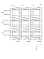
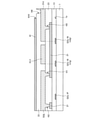
図21は、実施形態2に係るTFT基板の1画素において、ゲート線、半導体膜及び信号線の構成例を示す平面図である。図22は、実施形態2に係るTFT基板の1画素において、信号線及びドレインの構成例を示す平面図である。図22では、層間絶縁膜23で覆われている部位を破線で示している。図23は、実施形態2に係るTFT基板の1画素の構成例を示す平面図である。図23では、画素電極51で覆われている部位を破線で示している。また、図23では、図面の複雑化を回避するために、平坦化膜33(図9参照)、層間絶縁膜23及び絶縁膜13(図9参照)の図示を省略している。図24は、実施形態2に係るTFT基板において、隣り合う画素間におけるゲート線と半導体膜との関係を示す平面図である。
FIG. 21 is a plan view showing a configuration example of a gate line, a semiconductor film, and a signal line in one pixel of the TFT substrate according to the second embodiment. FIG. 22 is a plan view showing a configuration example of a signal line and a drain in one pixel of the TFT substrate according to the second embodiment. In FIG. 22, the portion covered with the
図21に示すように、実施形態2に係るTFT基板100Fは、ゲート線GCLと、ゲート線GCLと平面視で交差する信号線SGLと、信号線SGLに接続する半導体膜21と、を備える。ゲート線GCLは、第1ゲート線GCL-Nと、第1ゲート線GCL-NとY方向で隣り合う第2ゲート線GCL-Pと、を有する。
As shown in FIG. 21, the
第1ゲート線GCL-Nは、X方向に延設される第1ゲート主線GCL-Naと、第1ゲート主線GCL-Naに接続し、Y方向に延設される2本の第1ゲート副線GCL-Nb1、GCL-Nb2と、を有する。第1ゲート副線GCL-Nb1、GCL-Nb2は、第1ゲート主線GCL-NaからY方向に突き出ている。第1ゲート副線GCL-Nb1、GCL-Nb2は、1つの画素PXに1本ずつ配置されており、X方向で互いに隣り合っている。 The first gate line GCL-N is connected to the first gate main line GCL-Na extending in the X direction and the first gate main line GCL-Na, and is connected to the two first gate subs extending in the Y direction. It has lines GCL-Nb1 and GCL-Nb2. The first gate sub-lines GCL-Nb1 and GCL-Nb2 project in the Y direction from the first gate main line GCL-Na. The first gate sublines GCL-Nb1 and GCL-Nb2 are arranged one by one in one pixel PX, and are adjacent to each other in the X direction.
第2ゲート線GCL-Pは、X方向に延設される第2ゲート主線GCL-Paと、第2ゲート主線GCL-Paに接続し、Y方向に延設される2本の第2ゲート副線GCL-Pb1、GCL-Pb2と、を有する。第2ゲート副線GCL-Pb1、GCL-Pb2は、第2ゲート主線GCL-PaからY方向に突き出ている。第2ゲート副線GCL-Pb1、GCL-Pb2は、1つの画素PXに1本ずつ配置されており、X方向で互いに隣り合っている。 The second gate line GCL-P is connected to the second gate main line GCL-Pa extending in the X direction and the second gate main line GCL-Pa, and is connected to the two second gate subs extending in the Y direction. It has lines GCL-Pb1 and GCL-Pb2. The second gate sub-lines GCL-Pb1 and GCL-Pb2 project in the Y direction from the second gate main line GCL-Pa. The second gate sublines GCL-Pb1 and GCL-Pb2 are arranged one by one in one pixel PX, and are adjacent to each other in the X direction.
半導体膜21は、第1部位21aと、第2部位21bとを有する。第1部位21aは、信号線SGLとコンタクトホールH21を介して接続し、第1ゲート副線GCL-Nb1、GCL-Nb2とそれぞれ平面視で交差する。第2部位21bは、信号線SGLとコンタクトホールH22を介して接続し、第2ゲート副線GCL-Pb1、GCL-Pb2とそれぞれ平面視で交差する。第1部位21a及び第2部位21bの平面視による形状は、それぞれ直線状である。第1部位21a及び第2部位21bは、X方向に延設されている。
The
図22に示すように、半導体膜21上に層間絶縁膜23が設けられている。また、層間絶縁膜23上に信号線SGLとドレイン31dとが設けられている。半導体膜21の第1部位21aは、コンタクトホールH23を介してドレイン31dに接続している。コンタクトホールH21は、第1部位21aのX方向の一端部と重なる位置に設けられている。コンタクトホールH23は、第1部位21aのX方向の他端部と重なる位置に設けられている。また、半導体膜21の第2部位21bは、コンタクトホールH24を介してドレイン31dに接続している。コンタクトホールH22は、第2部位21bのX方向の一端部と重なる位置に設けられている。コンタクトホールH24は、第2部位21bのX方向の他端部と重なる位置に設けられている。
As shown in FIG. 22, the
また、図21に示すように、実施形態2に係るTFT基板100Fでは、第1ゲート主線GCL-Naと平面視で重なる領域に画素トランジスタTRは形成されない。TFT基板100Fでは、第1ゲート副線GCL-Nbと平面視で重なる領域に画素トランジスタTRが形成される。例えば、第1ゲート副線GCL-Nb1と半導体膜21の第1部位21aとが交差する位置に、第1NMOSトランジスタntr1が設けられている。また、第1ゲート副線GCL-Nb2と第1部位21aとが交差する位置に、第2NMOSトランジスタntr2が設けられている。第1ゲート主線GCL-Naの線幅は、画素トランジスタTRのゲート長に影響しない。このため、TFT基板100Fは、第1ゲート主線GCL-Naの線幅を、第1ゲート副線GCL-Nb1、GCL-Nb2の各線幅よりも細くすることができる。
Further, as shown in FIG. 21, in the
例えば、図22に示すように、TFT基板100Fにおいて、第1ゲート主線GCL-Naの線幅をW14とし、第1ゲート副線GCL-Nb2(または、第1ゲート副線GCL-Nb1の線幅)をW15としたとき、W14<W15であってもよい。これにより、TFT基板100Fは、W14≧W15の場合と比べて、第1ゲート線GCL-Nの寄生容量を低減することができる。
For example, as shown in FIG. 22, in the
同様に、図21に示すように、第2ゲート副線GCL-Pb1と半導体膜21の第2部位21bとが交差する位置に、第1PMOSトランジスタptr1が設けられている。また、第1ゲート副線GCL-Nb2と第2部位21bとが交差する位置に、第2NMOSトランジスタntr2が設けられている。第2ゲート主線GCL-Paの線幅は、画素トランジスタTRのゲート長に影響しない。このため、TFT基板100Fは、第2ゲート主線GCL-Paの線幅を、第2ゲート副線GCL-Pb1、GCL-Pb2の各線幅よりも細くすることができる。これにより、TFT基板100Fは、第2ゲート線GCL-Pの寄生容量を低減することができる。
Similarly, as shown in FIG. 21, the first polyclonal transistor ptr1 is provided at a position where the second gate sub-line GCL-Pb1 and the
また、信号線SGLの線幅をW31としたとき、W14<W31であってもよい。これにより、TFT基板100Fは、W14≧W31の場合と比べて、第1ゲート線GCL-Nの寄生容量を低減することができる。同様に、TFT基板100Fは、第2ゲート線GCL-Pの線幅も信号線SGLの線幅よりも細くしてよい。これにより、TFT基板100Fは、第2ゲート線GCL-Pの寄生容量を低減することができる。
Further, when the line width of the signal line SGL is W31, W14 <W31 may be satisfied. As a result, the
コンタクトホールH21、H22、H23、H24は、層間絶縁膜23に形成されている。また、図23に示すコンタクトホールH25は、平坦化膜33(図9参照)に形成されている。図23に示すように、ドレイン31dは、コンタクトホールH25を介して画素電極51に接続している。
The contact holes H21, H22, H23, and H24 are formed in the
図22に示すように、TFT基板100Fでは、第1NMOSトランジスタntr1のゲートのドレイン側と、第1PMOSトランジスタptr1のゲートのドレイン側とが、ドレイン31dと平面視で重なっている。また、第2NMOSトランジスタntr2のゲートの全領域と、第2PMOSトランジスタptr2のゲートの全領域とが、ドレイン31dと平面視で重なっている。
As shown in FIG. 22, in the
また、TFT基板100Fでは、各画素PXにおいて、第1ゲート副線GCL-Nb1、GCL-Nb2間のX方向の離隔距離は、第2ゲート副線GCL-Pb1、GCL-Pb2間の離隔距離と同じ値となっている。例えば、図21に示すように、第1ゲート副線GCL-Nb1、GCL-Nb2間のX方向の離隔距離をD20Nとし、第2ゲート副線GCL-Pb1、GCL-Pb2間の離隔距離をD20Pとしたとき、D20N=D20Pと同じ値となっている(D20N=D20P)。また、TFT基板100Fでは、第1ゲート副線GCL-Nb1と第2ゲート副線GCL-Pb1はX方向に互いに位置をずらして配置され、かつ、第1ゲート副線GCL-Nb2と第2ゲート副線GCL-Pb2もX方向に互いに位置をずらして配置されている。
Further, in the
これによれば、図24に示すように、Y方向で隣り合う画素PX間において、第1ゲート副線GCL-Nb1と第2ゲート副線GCL-Pb1は互いに対向しないようにすることができる。また、第1ゲート副線GCL-Nb1と第2ゲート副線GCL-Pb1は互いに対向しないようにすることができる。TFT基板100Fは、Y方向で隣り合う画素PX間のスペースを広げなくても、一方の画素PXの第1ゲート副線GCL-Nb1と他方の画素PXの第2ゲート副線GCL-Pb1との間のX方向の離隔距離D21を大きくすることができる。同様に、TFT基板100Fは、Y方向で隣り合う画素PX間のスペースを広げなくても、一方の画素PXの第1ゲート副線GCL-Nb2と他方の画素PXの第2ゲート副線GCL-Pb2との間のX方向の離隔距離D22を大きく確保することができる。これにより、TFT基板100Fは、Y方向で隣り合う画素PX間において、ゲート線GCL同士が互いに影響を及ぼし合うことを防ぐことができる。
According to this, as shown in FIG. 24, the first gate sub-line GCL-Nb1 and the second gate sub-line GCL-Pb1 can be prevented from facing each other between the adjacent pixels PX in the Y direction. Further, the first gate sub-line GCL-Nb1 and the second gate sub-line GCL-Pb1 can be prevented from facing each other. The
以上説明したように、実施形態2に係るTFT基板100Fは、X方向に延設されるゲート線GCLと、ゲート線GCLとは異なる層でY方向に延設され、ゲート線GCLと交差する信号線SGLと、ゲート線GCL及び信号線SGLとは異なる層に設けられ、ゲート線GCLと交差する半導体膜21と、ゲート線GCL及び半導体膜21とは異なる層に設けられ、ゲート線GCLと半導体膜21とが交差する領域の少なくとも一部を覆うドレイン31dと、を備える。これによれば、ドレイン31dの一部は、ドレイン31dよりも基材1側に位置する画素トランジスタTRのゲートを遮光することができる。
As described above, the
例えば、ドレイン31dは、第1NMOSトランジスタntr1のゲートのドレイン側と、第1PMOSトランジスタptr1のゲートのドレイン側と、第2NMOSトランジスタntr2のゲートの全領域と、第2PMOSトランジスタptr2のゲートの全領域とに重なる位置に配置されている。これによれば、画素トランジスタTRのゲートのうち、少なくともドレイン側の部位は遮光され、光電変換が抑制される。このため、TFT基板100Fは、画素トランジスタTRが誤作動する可能性を低減することができ、信頼性を向上させることができる。
For example, the
また、実施形態2に係るTFT基板100Fによれば、ゲート線GCLは、X方向に延設されるゲート主線(例えば、第1ゲート主線GCL-Na)と、ゲート主線から突き出た複数のゲート副線(例えば、第1ゲート副線GCL-Nb1、GCL-Nb2)と、を有する。半導体膜21は、信号線SGLからX方向に離れた位置でゲート主線及び複数のゲート副線と交差する。
Further, according to the
これによれば、画素トランジスタTRは、信号線SGLと重なる位置には配置されないため、半導体膜21と信号線SGLとが重なる領域の面積は最小限に抑えられる。例えば、TFT基板100Fは、半導体膜21と信号線SGLとが重なる領域を、半導体膜21と信号線SGLとが接続されるコンタクトホールH21の周辺と、コンタクトホールH22の周辺のみとすることができる。これにより、TFT基板100Fは、信号線SGLと半導体膜21との間の寄生容量を低減することができる。例えば、TFT基板100Fは、後述の実施形態3と比べて、半導体膜21と信号線SGLとが重なる領域の面積を小さくすることができ、信号線SGLと半導体膜21との間の寄生容量を低減することができる。
According to this, since the pixel transistor TR is not arranged at the position where it overlaps with the signal line SGL, the area of the region where the
また、ゲート線GCLは、第1ゲート線GCL-Nと、第1ゲート線GCL-NとY方向で隣り合う第2ゲート線GCL-Pと、を有する。第1ゲート線GCL-Nは、X方向に延設される第1ゲート主線GCL-Naと、第1ゲート主線GCL-Naから突き出た2本の第1ゲート副線GCL-Nb1、GCL-Nb2と、を有する。第2ゲート線GCL-Pは、X方向に延設される第2ゲート主線GCL-Paと、第2ゲート主線GCL-Paから突き出た2本の第2ゲート副線GCL-Pb1、GCL-Pb2と、を有する。半導体膜21は、信号線SGLからX方向に離れた位置で2本の第1ゲート副線GCL-Nb1、Nb2と交差する第1部位21aと、信号線SGLからX方向に離れた位置で2本の第2ゲート副線GCL-Pb1、GCL-Pb1と交差する第2部位21bと、を有する。
Further, the gate line GCL has a first gate line GCL-N and a second gate line GCL-P adjacent to the first gate line GCL-N in the Y direction. The first gate line GCL-N includes a first gate main line GCL-Na extending in the X direction and two first gate sub lines GCL-Nb1 and GCL-Nb2 protruding from the first gate main line GCL-Na. And have. The second gate line GCL-P includes a second gate main line GCL-Pa extending in the X direction and two second gate sub lines GCL-Pb1 and GCL-Pb2 protruding from the second gate main line GCL-Pa. And have. The
これによれば、TFT基板100Fは、画素トランジスタTRをCMOS(相補型MOS)構成とすることができる。TFT基板100Fは、画素トランジスタがCMOS構成ではない場合と比べて、NMOSトランジスタNTRとPMOSトランジスタPTRのそれぞれに印加される電圧振幅を小さくすることができ、画素トランジスタTRを構成するPMOSトランジスタPTR及びNMOSトランジスタNTRの耐圧を小さくすることができる。
According to this, the
実施形態2に係るTFT基板100Fの態様は、以下のように説明することもできる。
The embodiment of the
半導体膜21は、第1ゲート線GCL-Nに平行に延設される直線状の第1部位21a(本開示の第1直線部の一例)と、第2ゲート線GCL-Pに平行に延設される直線状の第2部位21b(本開示の第2直線部の一例)と、を有する。平面視において、第1ゲート線GCL-Nの第1ゲート主線GCL-Na及び第2ゲート線GCL-Pの第2ゲート主線GCL-Paは、第1部位21aと第2部位21bとの間に位置する。平面視において、ドレイン電極31dと画素電極51とを接続する平坦化膜33のコンタクトホールH25(本開示の第1コンタクトホールの一例)は、第1ゲート主線GCL-Naと第2ゲート主線GCL-Paの間に位置する。
The
層間絶縁膜23は、直線状の第1部位21a(本開示の第1直線部の一例)とドレイン電極31dとを接続するコンタクトホールH23(本開示の第6コンタクトホールの一例)と、直線状の第2部位21b(本開示の第2直線部の一例)とドレイン電極31dとを接続するコンタクトホールH24(本開示の第7コンタクトホールの一例)と、を備える。
The
層間絶縁膜23はさらに第1部位21aと信号線SGLを接続するコンタクトホールH21(本開示の第8コンタクトホールの一例)と、第2部位21bと信号線SGLを接続するコンタクトホールH22(本開示の第9コンタクトホール)を備える。
The
(変形例)
上記の実施形態2では、第1ゲート副線GCL-Nb1と第2ゲート副線GCL―Pb1はX方向に互いに位置をずらして配置され、第1ゲート副線GCL-Nb2と第2ゲート副線GCL―Pb2もX方向に互いに位置をずらして配置されていることを説明した。しかしながら、本実施形態において、ゲート線GCLの配置は、これに限定されない。
(Modification example)
In the second embodiment, the first gate sub-line GCL-Nb1 and the second gate sub-line GCL-Pb1 are arranged so as to be offset from each other in the X direction, and the first gate sub-line GCL-Nb2 and the second gate sub-line are arranged. It was explained that GCL-Pb2 is also arranged so as to be displaced from each other in the X direction. However, in the present embodiment, the arrangement of the gate line GCL is not limited to this.
図25は、実施形態2の変形例に係るTFT基板の構成例を示す平面図である。図25に示すように、実施形態2の変形例1に係るTFT基板100Gでは、1つの画素PX内で、第1ゲート副線GCL-Nb1及び第2ゲート副線GCL―Pb1は、Y方向で対向している。また、Y方向で隣り合う画素PX間でも、第1ゲート副線GCL-Nb及び第2ゲート副線GCL―Pbは、Y方向で対向している。このような構成であっても、TFT基板100Gは、遮光機能を備えたドレイン31dとを備えるため、信頼性を向上させることができる。また、TFT基板100Gにおいても、画素トランジスタTRは、信号線SGLと平面視で重なる位置には配置されない。このため、TFT基板100Gは、信号線SGLと半導体膜21との間の寄生容量を低減することができる。
FIG. 25 is a plan view showing a configuration example of the TFT substrate according to the modified example of the second embodiment. As shown in FIG. 25, in the
(実施形態3)
上記の実施形態1、2では、ゲート線GCLが、X方向に延設されたゲート主線と、Y方向に延設されたゲート副線とを有することを説明した。しかしながら、本実施形態において、ゲート線GCLの構成はこれに限定されない。ゲート線GCLは、X方向に延設されたゲート主線のみで構成されていてもよい。
(Embodiment 3)
In the
図26は、実施形態3に係るTFT基板の1画素において、ゲート線、半導体膜及び信号線の構成例を示す平面図である。図27は、実施形態3に係るTFT基板の1画素において、信号線及びドレインの構成例を示す平面図である。図27では、層間絶縁膜23で覆われている部位を破線で示している。図28は、実施形態3に係るTFT基板の1画素の構成例を示す平面図である。図28では、画素電極51で覆われている部位を破線で示している。また、図28では、図面の複雑化を回避するために、平坦化膜33(図29参照)、層間絶縁膜23及び絶縁膜13(図29参照)の図示を省略している。図29は、
図28に示す平面図をXXIX-XXIX’線で切断した断面図である。図30は、実施形態3に係るTFT基板において、隣り合う画素間におけるゲート線と半導体膜との関係を示す平面図である。
FIG. 26 is a plan view showing a configuration example of a gate line, a semiconductor film, and a signal line in one pixel of the TFT substrate according to the third embodiment. FIG. 27 is a plan view showing a configuration example of a signal line and a drain in one pixel of the TFT substrate according to the third embodiment. In FIG. 27, the portion covered with the
FIG. 28 is a cross-sectional view taken along the line XXIX-XXIX'from the plan view shown in FIG. 28. FIG. 30 is a plan view showing the relationship between the gate line and the semiconductor film between adjacent pixels in the TFT substrate according to the third embodiment.
図26に示すように、実施形態3に係るTFT基板100Hは、ゲート線GCLと、ゲート線GCLと平面視で交差する信号線SGLと、信号線SGLに接続する半導体膜21と、を備える。ゲート線GCLは、X方向に延設された第1ゲート線GCL-Nと、X方向に延設された第2ゲート線GCL-Pと、を有する。第1ゲート線GCL-Nと第2ゲート線GCL-Pは、それぞれ、X方向に延設されたゲート本線のみで構成されている。第1ゲート線GCL-Nと第2ゲート線GCL-Pは、Y方向で互いに隣り合っている。
As shown in FIG. 26, the
図26に示すように、半導体膜21の平面視による形状は、例えば、矩形の環状である。第1ゲート線GCL-Nは、環状の半導体膜21と平面視で交差する。第1ゲート線GCL-Nにおいて、環状の半導体膜21と平面視で交差する部位が、NMOSトランジスタNTRのゲートである。例えば、第1ゲート線GCL-Nにおいて、環状の半導体膜21と平面視で重なる2つの部位のうち、一方が第1NMOSトランジスタntr1のゲートであり、他方が第2NMOSトランジスタntr2のゲートである。
As shown in FIG. 26, the shape of the
同様に、第2ゲート線GCL-Pも、環状の半導体膜21と平面視で交差する。第2ゲート線GCL-Pにおいて、環状の半導体膜21と交差する部位が、PMOSトランジスタPTRのゲートである。例えば、第2ゲート線GCL-Pにおいて、環状の半導体膜21と平面視で重なる2つの部位のうち、一方が第1PMOSトランジスタptr1のゲートであり、他方が第2PMOSトランジスタptr2のゲートである。
Similarly, the second gate line GCL-P also intersects the
また、図27に示すように、半導体膜21の一部は信号線SGLと平面視で重なっている。信号線SGLと平面視で重なる領域に、第1NMOSトランジスタntr1と、第1PMOSトランジスタptr1とが配置されている。また、信号線SGLと平面視で重なる領域に、半導体膜21と信号線SGLとを接続するコンタクトホールH31が配置されている。
Further, as shown in FIG. 27, a part of the
図29に示すように、半導体膜21上に層間絶縁膜23が設けられている。また、層間絶縁膜23上に信号線SGLとドレイン31dとが設けられている。半導体膜21は、コンタクトホールH32を介してドレイン31dに接続している。コンタクトホールH32は、X方向において、コンタクトホールH1と対向する位置に設けられている。
As shown in FIG. 29, the
図26に示すように、実施形態3に係るTFT基板100Hでは、半導体膜21において、第1ゲート線GCL-N又は第2ゲート線GCL-Pと交差する部位の線幅W21は、信号線SGLの線幅W31の大きさ以下である(W21≦W31)。これにより、第1NMOSトランジスタntr1のゲートの全領域と、第1PMOSトランジスタptr1のゲートの全領域とが、信号線SGLで覆われている。また、図27に示すように、TFT基板100Hでは、第2NMOSトランジスタntr2のゲートのドレイン側と、第2PMOSトランジスタptr2のゲートのドレイン側とが、ドレイン31dで覆われている。
As shown in FIG. 26, in the
図29に示すように、コンタクトホールH31、H32は、層間絶縁膜23に形成されている。また、図28に示すコンタクトホールH33は、図29に示すように平坦化膜33に形成されている。ドレイン31dは、コンタクトホールH33を介して画素電極51に接続している。
As shown in FIG. 29, the contact holes H31 and H32 are formed in the
以上説明したように、実施形態3に係るTFT基板100Hは、X方向に延設されるゲート線GCLと、ゲート線GCLとは異なる層でY方向に延設され、ゲート線GCLと交差する信号線SGLと、ゲート線GCL及び信号線SGLとは異なる層に設けられ、ゲート線GCLと交差する半導体膜21と、ゲート線GCL及び半導体膜21とは異なる層に設けられ、ゲート線GCLと半導体膜21とが交差する領域の少なくとも一部を覆うドレイン31d及び信号線SGLと、を備える。これによれば、ドレイン31d及び信号線SGLは、これらよりも基材1側に位置する画素トランジスタTRのゲートを遮光することができる。
As described above, the
例えば、信号線SGLは、第1NMOSトランジスタntr1のゲートの全領域と、第1PMOSトランジスタptr1のゲートの全領域とに重なる位置に配置されている。ドレイン31dは、第2NMOSトランジスタntr2のゲートのドレイン側と、第2PMOSトランジスタptr2のゲートのドレイン側とに重なる位置に配置されている。一例を挙げると、図27に示すように、ドレイン31dのY方向における一端部311Aは、第2NMOSトランジスタntr2のゲートのドレイン側と重なる位置に配置されている。ドレイン31dのY方向における他端部311Bは、第2PMOSトランジスタptr2のゲートのドレイン側と重なる位置に配置されている。これによれば、画素トランジスタTRのゲートのうち、少なくともドレイン側の部位は遮光され、光電変換が抑制される。このため、TFT基板100Hは、画素トランジスタTRが誤作動する可能性を低減することができ、信頼性を向上させることができる。
For example, the signal line SGL is arranged at a position overlapping the entire region of the gate of the first NaCl transistor ntr1 and the entire region of the gate of the first polyclonal transistor ptr1. The
また、半導体膜21は、第1ゲート線GCL-Nに平行に延設される直線部211と、第2ゲート線GCL-Pに平行に延設される直線部212と、信号線SGLからX方向に離れた位置でゲート線CGLと交差する直線部213と、信号線SGLと重なる位置でゲート線CGLと交差する直線部214と、を有する。これによれば、直線部213は信号線SGLとは重ならない。このため、TFT基板100Hは、直線部213が信号線SGLと重なる場合と比べて、半導体膜21と信号線SGLとの間の寄生容量を低減することができる。
Further, the
また、ゲート線CGLは、X方向に延設される第1ゲート線CGL-Nと、第1ゲート線CGL-NとY方向で隣り合う第2ゲート線CGL-Pと、を有する。直線部213は、信号線SGLからX方向に離れた位置で第1ゲート線CGL-N及び第2ゲート線CGL-Pと交差する。直線部214は、信号線SGLと重なる位置で第1ゲート線CGL-N及び第2ゲート線CGL-Pと交差する。これによれば、TFT基板100Hは、画素トランジスタTRをCMOS(相補型MOS)構成とすることができる。TFT基板100Hは、画素トランジスタがCMOS構成ではない場合と比べて、NMOSトランジスタNTRとPMOSトランジスタPTRのそれぞれに印加される電圧振幅を小さくすることができ、画素トランジスタTRを構成するPMOSトランジスタPTR及びNMOSトランジスタNTRの耐圧を小さくすることができる。
Further, the gate line CGL has a first gate line CGL-N extending in the X direction and a second gate line CGL-P adjacent to the first gate line CGL-N in the Y direction. The
また、実施形態3に係るTFT基板100Hによれば、Y方向において、ゲート線CGLは半導体膜21の外縁よりも画素PXの中央側に位置する。このため、図30に示すように、Y方向で隣り合う画素PX間において、第1ゲート線CGL-Nと第2ゲート線CGL-Pとの間の離隔距離D23を広く確保しつつ、半導体膜21同士の離隔距離D31を狭くすることができる。これにより、TFT基板100Hは、さらなる高精細化が可能である。
Further, according to the
実施形態3に係るTFT基板100Hの態様は、以下のように説明することもできる。
The embodiment of the
半導体膜21は、第1ゲート線GCL-Nに平行に延設される直線部211(本開示の第1直線部の一例)と、第2ゲート線GCL-Pに平行に延設される直線部212(本開示の第2直線部の一例)と、を有する。平面視において、第1ゲート線GCL-N及び第2ゲート線GCL-Pは、直線部211と、直線部212との間に位置する。平面視において、ドレイン電極31dと画素電極51とを接続する平坦化膜33のコンタクトホールH33(本開示の第1コンタクトホールの一例)は、第1ゲート線GCL-Nと第2ゲート線GCL-Pの間に位置する。
The
また、半導体膜21は信号線SGLに平行に延設される直線部213(本開示の第3直線部の一例)を更に有する。直線部213は、直線部211と線部212とを接続する。
Further, the
また、直線部213とドレイン電極31dとを接続するコンタクトホールH32(本開示の第2コンタクトホールの一例)は、平面視において第1ゲート線GCL-Nと第2ゲート線GCL-Pの間に位置する。
Further, the contact hole H32 (an example of the second contact hole of the present disclosure) connecting the
半導体膜21は信号線SGLに平行に延設される直線部214(本開示の第4直線部の一例)を更に有する。直線部214は直線部211と直線部212とを接続する。信号線SGLは、層間絶縁膜23に形成されたコンタクトホールH31(本開示の第5コンタクトホールの一例)を介して直線部214と接続される。コンタクトホールH31は平面視において第1ゲート線GCL-Nと第2ゲート線GCL-Pとの間にある。
The
直線部211、212、213、214を有する半導体膜21の平面視による形状は、環状である。
The shape of the
直線部213は信号線SGLに重畳せず、直線部214は信号線SGLに重畳する。直線部213、214はそれぞれ第1ゲート線GCL-N及び第2ゲート線GCL-Pに交差する。
The
(変形例)
上述の実施形態1から3では、画素トランジスタTRはCMOS(相補型MOS)構成であり、NMOSトランジスタNTR及びPMOSトランジスタPTRの両方を有することを説明した。しかしながら、本実施形態において、画素トランジスタTRはCMOS(相補型MOS)構成に限定されない。画素トランジスタTRは、NMOSトランジスタNTR及びPMOSトランジスタPTRのうち、どちらか一方のみを有する構成であってもよい。
(Modification example)
In the above-described first to third embodiments, it has been described that the pixel transistor TR has a CMOS (complementary MOS) configuration and has both an IGMP transistor NTR and a polyclonal transistor PTR. However, in the present embodiment, the pixel transistor TR is not limited to the CMOS (complementary MOS) configuration. The pixel transistor TR may have a configuration having only one of the MIMO transistor NTR and the polyclonal transistor PTR.
図31は、実施形態3の変形例に係るTFT基板の構成例を示す平面図である。図32は、図31に示す平面図をXXXII-XXXII’線で切断した断面図である。実施形態3の変形例に係るTFT基板100Jにおいて、画素トランジスタTRは、NMOSトランジスタ、又は、PMOSトランジスタである。TFT基板100Jでは、1つの画素に1本のゲート線GCLが接続している。
FIG. 31 is a plan view showing a configuration example of the TFT substrate according to the modified example of the third embodiment. FIG. 32 is a cross-sectional view taken along the line XXXII-XXXII'of the plan view shown in FIG. 31. In the
図31に示すように、半導体膜21の平面視による形状は、例えば、U字状である。すなわち、半導体膜21は、直線部211、212、213を有する。直線部211の一方の端部に直線部212が接続し、直線部211の他方の端部に直線部213が接続している。直線部211と直線部212とが成す角度は約90°である。直線部211と直線部213とが成す角度も約90°である。
As shown in FIG. 31, the shape of the
図31に示すように、画素トランジスタTRは、第1MOSトランジスタtr1と、第2MOSトランジスタtr2とを有する。ゲート線GCLにおいて、半導体膜21の直線部213と交差する部位が、第1MOSトランジスタtr1のゲートである。ゲート線GCLにおいて、半導体膜21の直線部212と交差する部位が、第2MOSトランジスタtr2のゲートである。第1MOSトランジスタtr1と、第2MOSトランジスタtr2は直列に接続されている。
As shown in FIG. 31, the pixel transistor TR includes a first MOS transistor tr1 and a second MOS transistor tr2. In the gate line GCL, the portion intersecting the
実施形態3の変形例に係るTFT基板100Jは、実施形態3に係るTFT基板100Hと同様に、信頼性の向上と、高精細化が可能である。
Similar to the
以上、本発明の好適な実施の形態を説明したが、本発明はこのような実施の形態に限定されるものではない。実施の形態で開示された内容はあくまで一例にすぎず、本発明の趣旨を逸脱しない範囲で種々の変更が可能である。本発明の趣旨を逸脱しない範囲で行われた適宜の変更についても、当然に本発明の技術的範囲に属する。 Although the preferred embodiments of the present invention have been described above, the present invention is not limited to such embodiments. The contents disclosed in the embodiments are merely examples, and various changes can be made without departing from the spirit of the present invention. Appropriate changes made without departing from the spirit of the present invention naturally belong to the technical scope of the present invention.
1 基材
13 絶縁膜
21 半導体膜
23 層間絶縁膜
31d ドレイン
31s ソース
31r、31r1、31r2 遮光膜
33 平坦化膜
41 共通電極
45 絶縁膜
51 画素電極
100、100A、100B、100C、100D、100E、100F、100G、100H、100J TFT基板
110 ゲート駆動部
120 ソース駆動部
130 対向基板
131 基材
133 対向電極
160 電気泳動層
200 表示装置
C1 第1保持容量
C2 第2保持容量
GCL ゲート線
NTR NMOSトランジスタ
ntr1 第1NMOSトランジスタ
ntr2 第2NMOSトランジスタ
PTR PMOSトランジスタ
ptr1 第1PMOSトランジスタ
ptr2 第2PMOSトランジスタ
PX 画素
TR 画素トランジスタ
VCOM 共通電位
1
Claims (8)
前記第1ゲート線及び前記第2ゲート線と平面視で交差する信号線と、
前記信号線に接続する半導体膜と、
前記半導体膜に接続するドレイン電極と、
前記信号線と前記ドレイン電極を覆う平坦化膜と、
前記ドレイン電極に接続する画素電極と、を備え、
前記半導体膜は、前記第1ゲート線に平行に延設される第1直線部と、前記第2ゲート線に平行に延設される第2直線部と、前記信号線に平行に延設される第3直線部と、を有し、
平面視において、前記第1ゲート線及び前記第2ゲート線は、前記第1直線部と前記第2直線部との間に位置し、
平面視において、前記ドレイン電極と前記画素電極を接続する前記平坦化膜の第1コンタクトホールは、前記第1ゲート線と前記第2ゲート線の間に位置し、
前記第3直線部は、前記第1直線部と前記第2直線部とを接続し、
前記第3直線部は、前記第1ゲート線及び前記第2ゲート線と交差し、
前記第3直線部は、前記信号線と重畳しない、TFT基板。 The first gate line and the second gate line extending in the first direction,
A signal line that intersects the first gate line and the second gate line in a plan view,
The semiconductor film connected to the signal line and
The drain electrode connected to the semiconductor film and
A flattening film covering the signal line and the drain electrode,
A pixel electrode connected to the drain electrode is provided.
The semiconductor film is extended parallel to the signal line, a first straight line portion extending parallel to the first gate line, a second straight line portion extending parallel to the second gate line, and the signal line. It has a third straight line part and
In a plan view, the first gate line and the second gate line are located between the first straight line portion and the second straight line portion.
In a plan view, the first contact hole of the flattening film connecting the drain electrode and the pixel electrode is located between the first gate line and the second gate line .
The third straight line portion connects the first straight line portion and the second straight line portion.
The third straight line portion intersects the first gate line and the second gate line.
The third straight line portion is a TFT substrate that does not overlap with the signal line .
前記層間絶縁膜の前記第3直線部と前記ドレイン電極とを接続する第2コンタクトホールは、平面視において前記第1ゲート線と前記第2ゲート線の間に位置する、請求項1に記載のTFT基板。 An interlayer insulating film is provided between the semiconductor film and the drain electrode.
The first aspect of the present invention, wherein the second contact hole connecting the third straight line portion of the interlayer insulating film and the drain electrode is located between the first gate line and the second gate line in a plan view. TFT substrate.
前記第4直線部は前記第1直線部と前記第2直線部とを接続し、
前記信号線は前記層間絶縁膜に形成された第5コンタクトホールを介して前記第4直線部と接続され、
前記第5コンタクトホールは平面視において前記第1ゲート線と前記第2ゲート線との間にある、請求項2に記載のTFT基板。 The semiconductor film further has a fourth straight line portion extending parallel to the signal line.
The fourth straight line portion connects the first straight line portion and the second straight line portion.
The signal line is connected to the fourth straight line portion via a fifth contact hole formed in the interlayer insulating film.
The TFT substrate according to claim 2 , wherein the fifth contact hole is located between the first gate line and the second gate line in a plan view.
前記第1ゲート線に平行な第2ゲート線と、
前記第1ゲート線及び前記第2ゲート線と平面視で交差する信号線と、
前記第1ゲート線及び前記第2ゲート線と平面視で交差し、前記信号線に接続する半導体膜と、を備え、
前記半導体膜は、前記第1ゲート線に平行な第1直線部と、前記第2ゲート線に平行な第2直線部と、前記信号線に平行な第3直線部と、を有し、前記第3直線部は前記第1直線部と前記第2直線部とを接続し、
前記第3直線部は、前記第1ゲート線及び前記第2ゲート線に交差し、前記信号線に重畳しない、TFT基板。 The first gate line and
The second gate line parallel to the first gate line and
A signal line that intersects the first gate line and the second gate line in a plan view,
A semiconductor film that intersects the first gate line and the second gate line in a plan view and is connected to the signal line is provided.
The semiconductor film has a first straight line portion parallel to the first gate line, a second straight line portion parallel to the second gate line, and a third straight line portion parallel to the signal line. The third straight line portion connects the first straight line portion and the second straight line portion, and connects the first straight line portion.
The TFT substrate that the third straight line portion intersects the first gate line and the second gate line and does not superimpose on the signal line .
前記第4直線部は前記第1直線部と前記第2直線部とを接続し、
前記半導体膜の平面視による形状は環状である、請求項5に記載のTFT基板。 The semiconductor film further has a fourth straight line portion parallel to the signal line.
The fourth straight line portion connects the first straight line portion and the second straight line portion.
The TFT substrate according to claim 5 , wherein the shape of the semiconductor film in a plan view is annular.
前記基材の一方の面側に設けられる画素電極と、
前記基材と前記画素電極との間に設けられる画素トランジスタと、をさらに備え、
前記画素トランジスタは、
NMOSトランジスタと、
前記NMOSトランジスタに並列に接続するPMOSトランジスタと、を有し、
前記NMOSトランジスタのゲートは前記第1ゲート線に接続し、
前記NMOSトランジスタのソースは前記信号線に接続し、
前記NMOSトランジスタのドレインは前記画素電極に接続し、
前記PMOSトランジスタのゲートは前記第2ゲート線に接続し、
前記PMOSトランジスタのソースは前記信号線に接続し、
前記PMOSトランジスタのドレインは前記画素電極に接続している、請求項5から7のいずれか1項に記載のTFT基板。 Insulating base material and
A pixel electrode provided on one surface side of the base material and
Further, a pixel transistor provided between the base material and the pixel electrode is provided.
The pixel transistor is
With an MIMO transistor,
It has a epitaxial transistor connected in parallel to the NOTE transistor, and has.
The gate of the µtransistor is connected to the first gate line, and the gate is connected to the first gate line.
The source of the NOTE transistor is connected to the signal line and
The drain of the NOTE transistor is connected to the pixel electrode and
The gate of the polyclonal transistor is connected to the second gate line, and the gate is connected to the second gate line.
The source of the polyclonal transistor is connected to the signal line, and the source is connected to the signal line.
The TFT substrate according to any one of claims 5 to 7 , wherein the drain of the polyclonal transistor is connected to the pixel electrode.
Priority Applications (3)
| Application Number | Priority Date | Filing Date | Title |
|---|---|---|---|
| JP2018007271A JP6991865B2 (en) | 2018-01-19 | 2018-01-19 | TFT substrate |
| PCT/JP2018/047970 WO2019142638A1 (en) | 2018-01-19 | 2018-12-26 | Tft substrate |
| US16/930,744 US11171241B2 (en) | 2018-01-19 | 2020-07-16 | TFT substrate |
Applications Claiming Priority (1)
| Application Number | Priority Date | Filing Date | Title |
|---|---|---|---|
| JP2018007271A JP6991865B2 (en) | 2018-01-19 | 2018-01-19 | TFT substrate |
Publications (2)
| Publication Number | Publication Date |
|---|---|
| JP2019124890A JP2019124890A (en) | 2019-07-25 |
| JP6991865B2 true JP6991865B2 (en) | 2022-01-13 |
Family
ID=67301439
Family Applications (1)
| Application Number | Title | Priority Date | Filing Date |
|---|---|---|---|
| JP2018007271A Active JP6991865B2 (en) | 2018-01-19 | 2018-01-19 | TFT substrate |
Country Status (3)
| Country | Link |
|---|---|
| US (1) | US11171241B2 (en) |
| JP (1) | JP6991865B2 (en) |
| WO (1) | WO2019142638A1 (en) |
Families Citing this family (3)
| Publication number | Priority date | Publication date | Assignee | Title |
|---|---|---|---|---|
| CN114026629B (en) * | 2020-03-19 | 2023-12-19 | 京东方科技集团股份有限公司 | Display substrate and display device |
| JP7751416B2 (en) * | 2021-08-23 | 2025-10-08 | 株式会社ジャパンディスプレイ | Detection device |
| CN118284984A (en) * | 2021-11-22 | 2024-07-02 | 夏普显示科技株式会社 | Active matrix substrate and liquid crystal display device |
Citations (3)
| Publication number | Priority date | Publication date | Assignee | Title |
|---|---|---|---|---|
| JP2004241700A (en) | 2003-02-07 | 2004-08-26 | Seiko Epson Corp | Complementary thin film transistor circuit, electro-optical device, electronic equipment |
| JP2010085956A (en) | 2008-10-03 | 2010-04-15 | Seiko Epson Corp | Electro-optical device, electronic apparatus and projection type display device |
| JP2010239108A (en) | 2009-03-13 | 2010-10-21 | Seiko Epson Corp | Thin film semiconductor device, electro-optical device, and electronic apparatus |
Family Cites Families (2)
| Publication number | Priority date | Publication date | Assignee | Title |
|---|---|---|---|---|
| JPH02178632A (en) * | 1988-12-29 | 1990-07-11 | Sony Corp | Liquid crystal display device |
| JP2011221125A (en) | 2010-04-06 | 2011-11-04 | Seiko Epson Corp | Electro-optical device and driving method thereof, and electric equipment |
-
2018
- 2018-01-19 JP JP2018007271A patent/JP6991865B2/en active Active
- 2018-12-26 WO PCT/JP2018/047970 patent/WO2019142638A1/en not_active Ceased
-
2020
- 2020-07-16 US US16/930,744 patent/US11171241B2/en active Active
Patent Citations (3)
| Publication number | Priority date | Publication date | Assignee | Title |
|---|---|---|---|---|
| JP2004241700A (en) | 2003-02-07 | 2004-08-26 | Seiko Epson Corp | Complementary thin film transistor circuit, electro-optical device, electronic equipment |
| JP2010085956A (en) | 2008-10-03 | 2010-04-15 | Seiko Epson Corp | Electro-optical device, electronic apparatus and projection type display device |
| JP2010239108A (en) | 2009-03-13 | 2010-10-21 | Seiko Epson Corp | Thin film semiconductor device, electro-optical device, and electronic apparatus |
Also Published As
| Publication number | Publication date |
|---|---|
| US11171241B2 (en) | 2021-11-09 |
| US20200350438A1 (en) | 2020-11-05 |
| WO2019142638A1 (en) | 2019-07-25 |
| JP2019124890A (en) | 2019-07-25 |
Similar Documents
| Publication | Publication Date | Title |
|---|---|---|
| JP6999367B2 (en) | Substrate and electrophoresis equipment | |
| US9116407B2 (en) | Array substrate and manufacturing method thereof and display device | |
| JP5806383B2 (en) | Liquid crystal display | |
| JP6991865B2 (en) | TFT substrate | |
| JP6690671B2 (en) | Electro-optical device and electronic equipment | |
| US11658188B2 (en) | Array substrate and display device | |
| CN115079472B (en) | Electro-optical device and electronic apparatus | |
| JP7524745B2 (en) | Electro-optical devices and electronic equipment | |
| JP6791283B2 (en) | Electro-optics, electronic devices, and methods of manufacturing electro-optics | |
| JP2021043244A (en) | Electro-optical device and electronic apparatus | |
| JP6959359B2 (en) | Substrate and electrophoresis equipment | |
| JP7052844B2 (en) | Electro-optics and electronic devices | |
| JP7810046B2 (en) | Electro-optical devices and electronic equipment | |
| CN115079473B (en) | Electro-optical device and electronic apparatus | |
| JP6835122B2 (en) | Electro-optics and electronic equipment | |
| JP7463872B2 (en) | Electro-optical devices and electronic equipment | |
| JP2023147678A (en) | Electro-optic device and electronic apparatus | |
| JP2025029950A (en) | Electro-optical devices and electronic equipment | |
| JP2023147679A (en) | Electro-optic device and electronic apparatus | |
| JP2023147695A (en) | Electro-optic device and electronic apparatus | |
| JP2022091911A (en) | Electro-optics and electronic devices | |
| JP2022112864A (en) | electro-optical devices and electronics |
Legal Events
| Date | Code | Title | Description |
|---|---|---|---|
| A621 | Written request for application examination |
Free format text: JAPANESE INTERMEDIATE CODE: A621 Effective date: 20201125 |
|
| A131 | Notification of reasons for refusal |
Free format text: JAPANESE INTERMEDIATE CODE: A131 Effective date: 20210720 |
|
| A521 | Request for written amendment filed |
Free format text: JAPANESE INTERMEDIATE CODE: A523 Effective date: 20210917 |
|
| TRDD | Decision of grant or rejection written | ||
| A01 | Written decision to grant a patent or to grant a registration (utility model) |
Free format text: JAPANESE INTERMEDIATE CODE: A01 Effective date: 20211116 |
|
| A61 | First payment of annual fees (during grant procedure) |
Free format text: JAPANESE INTERMEDIATE CODE: A61 Effective date: 20211208 |
|
| R150 | Certificate of patent or registration of utility model |
Ref document number: 6991865 Country of ref document: JP Free format text: JAPANESE INTERMEDIATE CODE: R150 |
|
| R250 | Receipt of annual fees |
Free format text: JAPANESE INTERMEDIATE CODE: R250 |
|
| S111 | Request for change of ownership or part of ownership |
Free format text: JAPANESE INTERMEDIATE CODE: R313113 |
|
| R350 | Written notification of registration of transfer |
Free format text: JAPANESE INTERMEDIATE CODE: R350 |
|
| R250 | Receipt of annual fees |
Free format text: JAPANESE INTERMEDIATE CODE: R250 |