JP6971539B2 - Tungsten film with low fluorine content - Google Patents
Tungsten film with low fluorine content Download PDFInfo
- Publication number
- JP6971539B2 JP6971539B2 JP2016105216A JP2016105216A JP6971539B2 JP 6971539 B2 JP6971539 B2 JP 6971539B2 JP 2016105216 A JP2016105216 A JP 2016105216A JP 2016105216 A JP2016105216 A JP 2016105216A JP 6971539 B2 JP6971539 B2 JP 6971539B2
- Authority
- JP
- Japan
- Prior art keywords
- tungsten
- fluorine
- containing film
- less
- chamber
- Prior art date
- Legal status (The legal status is an assumption and is not a legal conclusion. Google has not performed a legal analysis and makes no representation as to the accuracy of the status listed.)
- Active
Links
Images


Classifications
-
- H—ELECTRICITY
- H01—ELECTRIC ELEMENTS
- H01L—SEMICONDUCTOR DEVICES NOT COVERED BY CLASS H10
- H01L21/00—Processes or apparatus adapted for the manufacture or treatment of semiconductor or solid state devices or of parts thereof
- H01L21/02—Manufacture or treatment of semiconductor devices or of parts thereof
- H01L21/04—Manufacture or treatment of semiconductor devices or of parts thereof the devices having at least one potential-jump barrier or surface barrier, e.g. PN junction, depletion layer or carrier concentration layer
- H01L21/18—Manufacture or treatment of semiconductor devices or of parts thereof the devices having at least one potential-jump barrier or surface barrier, e.g. PN junction, depletion layer or carrier concentration layer the devices having semiconductor bodies comprising elements of Group IV of the Periodic System or AIIIBV compounds with or without impurities, e.g. doping materials
- H01L21/28—Manufacture of electrodes on semiconductor bodies using processes or apparatus not provided for in groups H01L21/20 - H01L21/268
- H01L21/283—Deposition of conductive or insulating materials for electrodes conducting electric current
- H01L21/285—Deposition of conductive or insulating materials for electrodes conducting electric current from a gas or vapour, e.g. condensation
- H01L21/28506—Deposition of conductive or insulating materials for electrodes conducting electric current from a gas or vapour, e.g. condensation of conductive layers
- H01L21/28512—Deposition of conductive or insulating materials for electrodes conducting electric current from a gas or vapour, e.g. condensation of conductive layers on semiconductor bodies comprising elements of Group IV of the Periodic System
- H01L21/28556—Deposition of conductive or insulating materials for electrodes conducting electric current from a gas or vapour, e.g. condensation of conductive layers on semiconductor bodies comprising elements of Group IV of the Periodic System by chemical means, e.g. CVD, LPCVD, PECVD, laser CVD
-
- H—ELECTRICITY
- H01—ELECTRIC ELEMENTS
- H01L—SEMICONDUCTOR DEVICES NOT COVERED BY CLASS H10
- H01L21/00—Processes or apparatus adapted for the manufacture or treatment of semiconductor or solid state devices or of parts thereof
- H01L21/70—Manufacture or treatment of devices consisting of a plurality of solid state components formed in or on a common substrate or of parts thereof; Manufacture of integrated circuit devices or of parts thereof
- H01L21/71—Manufacture of specific parts of devices defined in group H01L21/70
- H01L21/768—Applying interconnections to be used for carrying current between separate components within a device comprising conductors and dielectrics
- H01L21/76838—Applying interconnections to be used for carrying current between separate components within a device comprising conductors and dielectrics characterised by the formation and the after-treatment of the conductors
- H01L21/76841—Barrier, adhesion or liner layers
- H01L21/76871—Layers specifically deposited to enhance or enable the nucleation of further layers, i.e. seed layers
- H01L21/76876—Layers specifically deposited to enhance or enable the nucleation of further layers, i.e. seed layers for deposition from the gas phase, e.g. CVD
-
- C—CHEMISTRY; METALLURGY
- C23—COATING METALLIC MATERIAL; COATING MATERIAL WITH METALLIC MATERIAL; CHEMICAL SURFACE TREATMENT; DIFFUSION TREATMENT OF METALLIC MATERIAL; COATING BY VACUUM EVAPORATION, BY SPUTTERING, BY ION IMPLANTATION OR BY CHEMICAL VAPOUR DEPOSITION, IN GENERAL; INHIBITING CORROSION OF METALLIC MATERIAL OR INCRUSTATION IN GENERAL
- C23C—COATING METALLIC MATERIAL; COATING MATERIAL WITH METALLIC MATERIAL; SURFACE TREATMENT OF METALLIC MATERIAL BY DIFFUSION INTO THE SURFACE, BY CHEMICAL CONVERSION OR SUBSTITUTION; COATING BY VACUUM EVAPORATION, BY SPUTTERING, BY ION IMPLANTATION OR BY CHEMICAL VAPOUR DEPOSITION, IN GENERAL
- C23C16/00—Chemical coating by decomposition of gaseous compounds, without leaving reaction products of surface material in the coating, i.e. chemical vapour deposition [CVD] processes
- C23C16/02—Pretreatment of the material to be coated
- C23C16/0272—Deposition of sub-layers, e.g. to promote the adhesion of the main coating
- C23C16/0281—Deposition of sub-layers, e.g. to promote the adhesion of the main coating of metallic sub-layers
-
- C—CHEMISTRY; METALLURGY
- C23—COATING METALLIC MATERIAL; COATING MATERIAL WITH METALLIC MATERIAL; CHEMICAL SURFACE TREATMENT; DIFFUSION TREATMENT OF METALLIC MATERIAL; COATING BY VACUUM EVAPORATION, BY SPUTTERING, BY ION IMPLANTATION OR BY CHEMICAL VAPOUR DEPOSITION, IN GENERAL; INHIBITING CORROSION OF METALLIC MATERIAL OR INCRUSTATION IN GENERAL
- C23C—COATING METALLIC MATERIAL; COATING MATERIAL WITH METALLIC MATERIAL; SURFACE TREATMENT OF METALLIC MATERIAL BY DIFFUSION INTO THE SURFACE, BY CHEMICAL CONVERSION OR SUBSTITUTION; COATING BY VACUUM EVAPORATION, BY SPUTTERING, BY ION IMPLANTATION OR BY CHEMICAL VAPOUR DEPOSITION, IN GENERAL
- C23C16/00—Chemical coating by decomposition of gaseous compounds, without leaving reaction products of surface material in the coating, i.e. chemical vapour deposition [CVD] processes
- C23C16/04—Coating on selected surface areas, e.g. using masks
- C23C16/045—Coating cavities or hollow spaces, e.g. interior of tubes; Infiltration of porous substrates
-
- C—CHEMISTRY; METALLURGY
- C23—COATING METALLIC MATERIAL; COATING MATERIAL WITH METALLIC MATERIAL; CHEMICAL SURFACE TREATMENT; DIFFUSION TREATMENT OF METALLIC MATERIAL; COATING BY VACUUM EVAPORATION, BY SPUTTERING, BY ION IMPLANTATION OR BY CHEMICAL VAPOUR DEPOSITION, IN GENERAL; INHIBITING CORROSION OF METALLIC MATERIAL OR INCRUSTATION IN GENERAL
- C23C—COATING METALLIC MATERIAL; COATING MATERIAL WITH METALLIC MATERIAL; SURFACE TREATMENT OF METALLIC MATERIAL BY DIFFUSION INTO THE SURFACE, BY CHEMICAL CONVERSION OR SUBSTITUTION; COATING BY VACUUM EVAPORATION, BY SPUTTERING, BY ION IMPLANTATION OR BY CHEMICAL VAPOUR DEPOSITION, IN GENERAL
- C23C16/00—Chemical coating by decomposition of gaseous compounds, without leaving reaction products of surface material in the coating, i.e. chemical vapour deposition [CVD] processes
- C23C16/06—Chemical coating by decomposition of gaseous compounds, without leaving reaction products of surface material in the coating, i.e. chemical vapour deposition [CVD] processes characterised by the deposition of metallic material
- C23C16/08—Chemical coating by decomposition of gaseous compounds, without leaving reaction products of surface material in the coating, i.e. chemical vapour deposition [CVD] processes characterised by the deposition of metallic material from metal halides
- C23C16/14—Deposition of only one other metal element
-
- C—CHEMISTRY; METALLURGY
- C23—COATING METALLIC MATERIAL; COATING MATERIAL WITH METALLIC MATERIAL; CHEMICAL SURFACE TREATMENT; DIFFUSION TREATMENT OF METALLIC MATERIAL; COATING BY VACUUM EVAPORATION, BY SPUTTERING, BY ION IMPLANTATION OR BY CHEMICAL VAPOUR DEPOSITION, IN GENERAL; INHIBITING CORROSION OF METALLIC MATERIAL OR INCRUSTATION IN GENERAL
- C23C—COATING METALLIC MATERIAL; COATING MATERIAL WITH METALLIC MATERIAL; SURFACE TREATMENT OF METALLIC MATERIAL BY DIFFUSION INTO THE SURFACE, BY CHEMICAL CONVERSION OR SUBSTITUTION; COATING BY VACUUM EVAPORATION, BY SPUTTERING, BY ION IMPLANTATION OR BY CHEMICAL VAPOUR DEPOSITION, IN GENERAL
- C23C16/00—Chemical coating by decomposition of gaseous compounds, without leaving reaction products of surface material in the coating, i.e. chemical vapour deposition [CVD] processes
- C23C16/44—Chemical coating by decomposition of gaseous compounds, without leaving reaction products of surface material in the coating, i.e. chemical vapour deposition [CVD] processes characterised by the method of coating
- C23C16/455—Chemical coating by decomposition of gaseous compounds, without leaving reaction products of surface material in the coating, i.e. chemical vapour deposition [CVD] processes characterised by the method of coating characterised by the method used for introducing gases into reaction chamber or for modifying gas flows in reaction chamber
- C23C16/45523—Pulsed gas flow or change of composition over time
- C23C16/45525—Atomic layer deposition [ALD]
-
- H—ELECTRICITY
- H01—ELECTRIC ELEMENTS
- H01L—SEMICONDUCTOR DEVICES NOT COVERED BY CLASS H10
- H01L21/00—Processes or apparatus adapted for the manufacture or treatment of semiconductor or solid state devices or of parts thereof
- H01L21/02—Manufacture or treatment of semiconductor devices or of parts thereof
- H01L21/02104—Forming layers
- H01L21/02107—Forming insulating materials on a substrate
- H01L21/02225—Forming insulating materials on a substrate characterised by the process for the formation of the insulating layer
- H01L21/0226—Forming insulating materials on a substrate characterised by the process for the formation of the insulating layer formation by a deposition process
- H01L21/02263—Forming insulating materials on a substrate characterised by the process for the formation of the insulating layer formation by a deposition process deposition from the gas or vapour phase
- H01L21/02271—Forming insulating materials on a substrate characterised by the process for the formation of the insulating layer formation by a deposition process deposition from the gas or vapour phase deposition by decomposition or reaction of gaseous or vapour phase compounds, i.e. chemical vapour deposition
- H01L21/0228—Forming insulating materials on a substrate characterised by the process for the formation of the insulating layer formation by a deposition process deposition from the gas or vapour phase deposition by decomposition or reaction of gaseous or vapour phase compounds, i.e. chemical vapour deposition deposition by cyclic CVD, e.g. ALD, ALE, pulsed CVD
-
- H—ELECTRICITY
- H01—ELECTRIC ELEMENTS
- H01L—SEMICONDUCTOR DEVICES NOT COVERED BY CLASS H10
- H01L21/00—Processes or apparatus adapted for the manufacture or treatment of semiconductor or solid state devices or of parts thereof
- H01L21/02—Manufacture or treatment of semiconductor devices or of parts thereof
- H01L21/04—Manufacture or treatment of semiconductor devices or of parts thereof the devices having at least one potential-jump barrier or surface barrier, e.g. PN junction, depletion layer or carrier concentration layer
- H01L21/18—Manufacture or treatment of semiconductor devices or of parts thereof the devices having at least one potential-jump barrier or surface barrier, e.g. PN junction, depletion layer or carrier concentration layer the devices having semiconductor bodies comprising elements of Group IV of the Periodic System or AIIIBV compounds with or without impurities, e.g. doping materials
- H01L21/28—Manufacture of electrodes on semiconductor bodies using processes or apparatus not provided for in groups H01L21/20 - H01L21/268
- H01L21/28008—Making conductor-insulator-semiconductor electrodes
- H01L21/28017—Making conductor-insulator-semiconductor electrodes the insulator being formed after the semiconductor body, the semiconductor being silicon
- H01L21/28158—Making the insulator
- H01L21/28167—Making the insulator on single crystalline silicon, e.g. using a liquid, i.e. chemical oxidation
- H01L21/28194—Making the insulator on single crystalline silicon, e.g. using a liquid, i.e. chemical oxidation by deposition, e.g. evaporation, ALD, CVD, sputtering, laser deposition
-
- H—ELECTRICITY
- H01—ELECTRIC ELEMENTS
- H01L—SEMICONDUCTOR DEVICES NOT COVERED BY CLASS H10
- H01L21/00—Processes or apparatus adapted for the manufacture or treatment of semiconductor or solid state devices or of parts thereof
- H01L21/02—Manufacture or treatment of semiconductor devices or of parts thereof
- H01L21/04—Manufacture or treatment of semiconductor devices or of parts thereof the devices having at least one potential-jump barrier or surface barrier, e.g. PN junction, depletion layer or carrier concentration layer
- H01L21/18—Manufacture or treatment of semiconductor devices or of parts thereof the devices having at least one potential-jump barrier or surface barrier, e.g. PN junction, depletion layer or carrier concentration layer the devices having semiconductor bodies comprising elements of Group IV of the Periodic System or AIIIBV compounds with or without impurities, e.g. doping materials
- H01L21/28—Manufacture of electrodes on semiconductor bodies using processes or apparatus not provided for in groups H01L21/20 - H01L21/268
- H01L21/283—Deposition of conductive or insulating materials for electrodes conducting electric current
- H01L21/285—Deposition of conductive or insulating materials for electrodes conducting electric current from a gas or vapour, e.g. condensation
- H01L21/28506—Deposition of conductive or insulating materials for electrodes conducting electric current from a gas or vapour, e.g. condensation of conductive layers
- H01L21/28512—Deposition of conductive or insulating materials for electrodes conducting electric current from a gas or vapour, e.g. condensation of conductive layers on semiconductor bodies comprising elements of Group IV of the Periodic System
- H01L21/28556—Deposition of conductive or insulating materials for electrodes conducting electric current from a gas or vapour, e.g. condensation of conductive layers on semiconductor bodies comprising elements of Group IV of the Periodic System by chemical means, e.g. CVD, LPCVD, PECVD, laser CVD
- H01L21/28562—Selective deposition
-
- H—ELECTRICITY
- H01—ELECTRIC ELEMENTS
- H01L—SEMICONDUCTOR DEVICES NOT COVERED BY CLASS H10
- H01L21/00—Processes or apparatus adapted for the manufacture or treatment of semiconductor or solid state devices or of parts thereof
- H01L21/70—Manufacture or treatment of devices consisting of a plurality of solid state components formed in or on a common substrate or of parts thereof; Manufacture of integrated circuit devices or of parts thereof
- H01L21/71—Manufacture of specific parts of devices defined in group H01L21/70
- H01L21/768—Applying interconnections to be used for carrying current between separate components within a device comprising conductors and dielectrics
- H01L21/76838—Applying interconnections to be used for carrying current between separate components within a device comprising conductors and dielectrics characterised by the formation and the after-treatment of the conductors
- H01L21/76877—Filling of holes, grooves or trenches, e.g. vias, with conductive material
-
- H—ELECTRICITY
- H01—ELECTRIC ELEMENTS
- H01L—SEMICONDUCTOR DEVICES NOT COVERED BY CLASS H10
- H01L21/00—Processes or apparatus adapted for the manufacture or treatment of semiconductor or solid state devices or of parts thereof
- H01L21/70—Manufacture or treatment of devices consisting of a plurality of solid state components formed in or on a common substrate or of parts thereof; Manufacture of integrated circuit devices or of parts thereof
- H01L21/71—Manufacture of specific parts of devices defined in group H01L21/70
- H01L21/768—Applying interconnections to be used for carrying current between separate components within a device comprising conductors and dielectrics
- H01L21/76898—Applying interconnections to be used for carrying current between separate components within a device comprising conductors and dielectrics formed through a semiconductor substrate
-
- H—ELECTRICITY
- H01—ELECTRIC ELEMENTS
- H01L—SEMICONDUCTOR DEVICES NOT COVERED BY CLASS H10
- H01L2924/00—Indexing scheme for arrangements or methods for connecting or disconnecting semiconductor or solid-state bodies as covered by H01L24/00
- H01L2924/01—Chemical elements
- H01L2924/01009—Fluorine [F]
-
- H—ELECTRICITY
- H01—ELECTRIC ELEMENTS
- H01L—SEMICONDUCTOR DEVICES NOT COVERED BY CLASS H10
- H01L2924/00—Indexing scheme for arrangements or methods for connecting or disconnecting semiconductor or solid-state bodies as covered by H01L24/00
- H01L2924/01—Chemical elements
- H01L2924/01074—Tungsten [W]
Description
化学気相堆積(CVD)技術を用いるタングステン含有材料の堆積は、多くの半導体製造プロセスに不可欠な部分である。このような材料は、水平方向の相互接続、隣接する金属層間のビア、シリコン基板上の第1の金属層とデバイスとの間の接触、およびアスペクト比の高い特徴部に対して使用され得る。従来の堆積プロセスでは、基板が堆積チャンバ内で所定の処理温度まで加熱され、シードまたは核形成層としての役割を果たすタングステン含有材料の薄層が堆積される。その後、残りのタングステン含有材料(バルク層)は、核形成層上に堆積される。通常、タングステン含有材料は、六フッ化タングステン(WF6)の還元によって形成される。 Tungsten-containing material deposition using chemical vapor deposition (CVD) technology is an integral part of many semiconductor manufacturing processes. Such materials can be used for horizontal interconnections, vias between adjacent metal layers, contact between the first metal layer on a silicon substrate and the device, and features with a high aspect ratio. In a conventional deposition process, the substrate is heated to a predetermined treatment temperature in the deposition chamber to deposit a thin layer of tungsten-containing material that acts as a seed or nucleation layer. The remaining tungsten-containing material (bulk layer) is then deposited on the nucleation layer. Tungsten-containing materials are typically formed by reduction of tungsten hexafluoride (WF 6).
本明細書に記載した主題の一態様は、低フッ素のタングステン含有膜を基板上に堆積させる方法に関する。本方法は、フッ素含有タングステン前駆体と還元剤との交互のパルス(pulse)に基板を曝露し、これによってタングステン含有膜を基板に堆積させることを含み、フッ素含有タングステン前駆体がパルスを発生させている間、基板を収容しているチャンバのチャンバ圧力は10トル未満である。タングステン含有膜中のフッ素濃度は、1019原子/cm3未満であってよい。実施形態によっては、タングステン膜中のフッ素濃度は1018原子/cm3未満である様々な実施形態によれば、チャンバ圧力は、7トル未満または5トル未満であってよい。実施形態によっては、タングステン含有膜は、タングステン核形成層である。実施形態によっては、タングステン含有膜は、フッ素を含まないプロセスを介して堆積された第1のタングステン含有膜上に堆積される。実施形態によっては、タングステン含有膜は、バリア層上に堆積される。還元剤の例には、シリコン含有還元剤、ホウ素含有還元剤、およびゲルマニウム含有還元剤がある。実施形態によっては、フッ素含有タングステン前駆体のパルスは水素(H2)を含んでいる。様々な実施形態によれば、タングステン含有膜は抵抗率が低く、例えば130μΩ/cm未満または110μΩ/cm未満であってよい。本方法は、タングステン含有膜上への化学気相堆積(CVD)によってタングステンバルク層を堆積させることをさらに含む。 One aspect of the subject matter described herein relates to a method of depositing a low fluorine tungsten-containing film on a substrate. The method comprises exposing the substrate to alternating pulses of fluorine-containing tungsten precursors and reducing agents, thereby depositing a tungsten-containing film on the substrate, which causes the fluorine-containing tungsten precursors to generate pulses. Meanwhile, the chamber pressure of the chamber containing the substrate is less than 10 tons. Fluorine concentration in the tungsten-containing film may be less than 10 19 atoms / cm 3. In some embodiments, the fluorine concentration in the tungsten film is less than 10 18 atoms / cm 3 , and according to various embodiments, the chamber pressure may be less than 7 torr or less than 5 torr. In some embodiments, the tungsten-containing film is a tungsten nucleation layer. In some embodiments, the tungsten-containing film is deposited on a first tungsten-containing film deposited via a fluorine-free process. In some embodiments, the tungsten-containing film is deposited on the barrier layer. Examples of reducing agents include silicon-containing reducing agents, boron-containing reducing agents, and germanium-containing reducing agents. In some embodiments, the pulse of the fluorine-containing tungsten precursor contains hydrogen (H 2 ). According to various embodiments, the tungsten-containing film has a low resistivity, for example, less than 130 μΩ / cm or less than 110 μΩ / cm. The method further comprises depositing a tungsten bulk layer by chemical vapor deposition (CVD) on a tungsten-containing membrane.
本明細書に記載した主題の別の態様は、フッ素を含まないプロセスによって第1のタングステン含有膜を基板上に堆積させることと、フッ素含有前駆体を用いる原子層の堆積によって第2のタングステン含有膜を第1のタングステン膜に堆積させることとを含む方法であって、第2のタングステン含有膜の堆積中、基板を収容しているチャンバのチャンバ圧力が10トル未満である、方法に関する。実施形態によっては、第1のタングステン含有膜は、バリア層上に堆積される。実施形態によっては、第1のタングステン含有膜は、酸化シリコン上に堆積される。様々な実施形態によれば、チャンバ圧力は、7トル未満または5トル未満であってよい。様々な実施形態によれば、第2のタングステン含有膜中のフッ素濃度は、1019原子/cm3未満または1018原子/cm3未満である。 Another aspect of the subject matter described herein is to deposit a first tungsten-containing film on a substrate by a fluorine-free process and to deposit a second tungsten-containing layer by depositing an atomic layer with a fluorine-containing precursor. A method comprising depositing a film on a first tungsten film, wherein the chamber pressure of the chamber containing the substrate is less than 10 tolls during the deposition of the second tungsten-containing film. In some embodiments, the first tungsten-containing film is deposited on the barrier layer. In some embodiments, the first tungsten-containing film is deposited on silicon oxide. According to various embodiments, the chamber pressure may be less than 7 torr or less than 5 torr. According to various embodiments, the fluorine concentration in the second tungsten-containing film is less than 10 19 atoms / cm 3 or less than 10 18 atoms / cm 3 .
本明細書に記載のいずれかの方法を実施するように構成された装置には、さらに他の態様を実施できる。例えば、本明細書に記載した主題の別の態様は、基板を処理する装置であって、(a)基板を保持するように構成された基台を備える少なくとも1つの処理チャンバと、(b)真空空間に連結させるための少なくとも1つの出口と、(c)1つ以上の処理ガス供給源に連結している1つ以上の処理ガス入口と、(d)装置内の動作を制御するためのコントローラであって、還元剤とフッ素含有タングステン前駆体とを交互にパルスした状態で処理チャンバに導入するための機械可読命令を含むコントローラと、を備える装置において、チャンバ圧力は10トル未満である、装置に関する。 Yet another embodiment can be implemented for devices configured to perform any of the methods described herein. For example, another aspect of the subject described herein is a device for processing a substrate, wherein (a) at least one processing chamber with a base configured to hold the substrate, and (b). At least one outlet for connecting to a vacuum space, (c) one or more treated gas inlets connected to one or more treated gas sources, and (d) controlling operation within the device. In a device comprising a controller comprising a machine-readable instruction for introducing a reducing agent and a fluorine-containing tungsten precursor in alternating pulses into the processing chamber, the chamber pressure is less than 10 torr. Regarding the device.
これらの態様およびその他の態様を、図面を参照してさらに説明する。 These and other aspects will be further described with reference to the drawings.
以下の説明では、本発明を徹底して理解してもらうために、数多くの具体的な詳細を記載している。本発明は、そのような具体的な詳細の一部または全部がなくとも実施され得る。また、本発明を無駄に不明瞭にしないように、公知の処理作業は記載していない。本発明を具体的な実施形態とともに説明していくが、それは本発明をその実施形態に限定することを意図するものではないことが理解されるであろう。 In the following description, a number of specific details are given in order to give a thorough understanding of the present invention. The present invention may be practiced without some or all of such specific details. In addition, known processing operations are not described so as not to unnecessarily obscure the present invention. The present invention will be described with specific embodiments, but it will be understood that it is not intended to limit the invention to that embodiment.
本明細書に記載するのは、タングステン堆積方法ならびにそれに関連するシステムおよび装置である。適応例には、ロジックとメモリとの接点の充填、DRAM埋め込みワード線の充填、垂直に埋め込まれたメモリゲート/ワード線の充填、およびシリコン貫通ビア(TSV)による三次元集積化などがある。実施形態によっては、本方法は、タングステンの特徴部を充填するために使用されてよい。そのような特徴部として、ビアなどの垂直方向の特徴部、および垂直方向のNAND(VNAND)ワード線などの水平特徴部を挙げることができる。本方法は、等角式またはボトムアップ/インサイドアウト式の充填に使用されてよい。 Described herein are tungsten deposition methods and related systems and equipment. Examples of applications include filling of contacts between logic and memory, filling of DRAM embedded word lines, filling of vertically embedded memory gates / word lines, and three-dimensional integration with silicon penetrating vias (TSVs). In some embodiments, the method may be used to fill the features of tungsten. Examples of such a feature include a vertical feature such as a via and a horizontal feature such as a vertical NAND (VNAND) word line. The method may be used for equiangular or bottom-up / inside-out filling.
本明細書に記載の方法および装置の態様は、タングステン核形成層などのタングステン含有層の堆積に関する。本方法の様々な実施形態では、基板を低チャンバ圧力でタングステン前駆体と還元剤とのパルスに交互に曝露し、それによってタングステン核形成層を基板の表面に堆積させることを必要とする。様々な実施形態によれば、チャンバ圧力は、10トル以下に維持されてよい。実施形態によっては、チャンバ圧力は、7トル以下、あるいはそれよりも低い5トル以下などに維持されてよい。本方法は、フッ素含有タングステン前駆体を用いて実施されてもよいが、堆積された核形成層中のフッ素は極めて少量または検出不可能な量になることがある。 Aspects of the methods and devices described herein relate to the deposition of tungsten-containing layers such as tungsten nucleation layers. Various embodiments of the method require alternating exposure of the substrate to pulses of tungsten precursor and reducing agent at low chamber pressures thereby depositing a tungsten cambium on the surface of the substrate. According to various embodiments, the chamber pressure may be maintained below 10 torr. Depending on the embodiment, the chamber pressure may be maintained at 7 torr or less, or even lower, 5 torr or less. The method may be carried out with a fluorine-containing tungsten precursor, but the amount of fluorine in the deposited cambium can be very small or undetectable.
図1A〜1Gは、本明細書に記載のプロセスに従い、フッ素含有前駆体を用いて低フッ素層を堆積させてよい様々構造の概略例の図である。実施形態によっては、構造は、タングステンまたはタングステン含有材料が充填される特徴部を備えている。実施形態によっては、特徴部は、以下のうちの1つ以上を特徴とすることができる:狭い開口が、凹型の開口、窮屈な特徴部内部、高アスペクト比。図1Aは、タングステンが充填される垂直方向の特徴部101の断面図の一例を示している。特徴部は、基板103に特徴部の穴105を備えることができる。基板は、シリコンウエハであってよく、例えば、基板上に堆積される誘電性、導電性、または半導電性の材料などの層を1つ以上有するウエハを含む200−mmのウエハ、300−mmのウエハ、または450−mmのウエハであってよい。特徴部は、1つ以上のこれらの層で形成されてよい。例えば、特徴部は、少なくとも部分的に誘電層に形成されてよい。実施形態によっては、特徴部の穴105は、アスペクト比が少なくとも約2:1、少なくとも約4:1、少なくとも約6:1またはこれ以上であってもよい。特徴部の穴105は、開口、例えば開口の直径またはライン幅に近い寸法であってもよく、約10nm〜500nm、例えば約25nm〜300nmであってもよい。特徴部の穴105を、未充填の特徴部または単に特徴部と呼ぶことができる。特徴部101、および任意の特徴は、部分的に、特徴部の長さに沿って延びる軸118を特徴とすることができ、垂直方向を向いている特徴部は垂直軸を有し、水平方向を向いている特徴部は水平軸を有する。
FIGS. 1A-1G are schematic examples of various structures in which a low fluorine layer may be deposited using a fluorine-containing precursor according to the process described herein. In some embodiments, the structure comprises features that are filled with tungsten or a tungsten-containing material. In some embodiments, the feature may be characterized by one or more of the following: narrow openings, concave openings, cramped feature interiors, high aspect ratios. FIG. 1A shows an example of a cross-sectional view of a
図1Bは、凹状の輪郭を有する特徴部101の一例を示している。凹状の輪郭とは、底、閉じた端部、または特徴部の内部から特徴部の開口まで狭くなる輪郭である。様々な実施形態によれば、輪郭は、徐々に狭くなり、かつ/または特徴部の開口に隆起部を備えていてよい。図1Bは、後者の一例を示しており、特徴部の穴105の側壁または内面を内張する下層113がある。下層113は、例えば、拡散障壁層、接着層、核形成層、これらの組み合わせ、またはその他の任意の適用可能な材料であり得る。下層の非限定的な例として、誘電層および導電層、例えば酸化シリコン、窒化シリコン、炭化シリコン、金属酸化物、金属窒化物、金属炭化物、および金属の層などが挙げられる。特定の実施形態では、下層は、1つ以上のTi、TiN、WN、TiAl、およびWであり得る。下層113は、下層113が特徴部101の開口近くで特徴部101の内部よりも厚くなるように隆起部115を形成する。
FIG. 1B shows an example of a
実施形態によっては、特徴部内に1つ以上のくびれ部を有する特徴部が充填されてもよい。図1Cは、くびれ部を有する特徴部に充填した様々な図の例を示している。図1Cの例(a)、(b)および(c)の各々は、特徴部内の中間点にくびれ部109を備えている。くびれ部109は、例えば幅が約15nm〜20nmであり得る。くびれ部は、従来の技術を用いて特徴部にタングステンを堆積させる過程でピンチオフを起こすことができ、堆積されたタングステンが、特徴部のその部分が充填される前に新たな堆積物がくびれ部を通って特徴部にボイドができてしまうのを阻止する。例(b)は、特徴部の開口にライナー/バリア隆起部115をさらに備えている。このような隆起部は、潜在的なピンチオフ点でもあり得る。例(c)は、例(b)の隆起部115よりもフィールド領域から離れているくびれ部112を備えている。
Depending on the embodiment, the feature portion having one or more constricted portions may be filled in the feature portion. FIG. 1C shows examples of various figures filled in a feature portion having a constricted portion. Each of the examples (a), (b) and (c) of FIG. 1C has a constricted
3Dメモリ構造などの水平特徴部を充填することもできる。図1Dは、くびれ部151を備えている水平特徴部150の一例を示している。例えば、水平特徴部150は、VNAND構造内のワード線であってよい。
It is also possible to fill a horizontal feature such as a 3D memory structure. FIG. 1D shows an example of a
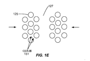
実施形態によっては、くびれ部は、VNANDまたはその他の構造に支柱があることによって発生し得る。例えば図1Eは、VNANDまたは垂直に集積したメモリ(VIM:vertically integrated memory)の構造148にある支柱125の平面図を示し、図1Fは、支柱125の簡易な概略断面図を示している。図1E内の矢印は、材料の堆積を表している。支柱125は領域127とガスの入口またはその他の堆積源との間に配置されるため、隣接する支柱どうしがくびれ部151をもたらすことができ、このくびれ部は、領域127にボイドなしで充填する際の課題を備えている。
In some embodiments, the constriction can be caused by the presence of stanchions in the VN NAND or other structure. For example, FIG. 1E shows a plan view of a
構造148は、例えば、層間絶縁層154と犠牲層(図示せず)が基板100上で交互になっているスタックを堆積し、犠牲層を選択的にエッチングすることによって形成され得る。層間絶縁層は、例えば、エッチング液を用いて選択的にエッチング可能な材料の犠牲層を含む酸化シリコンおよび/または窒化シリコンの層であってよい。これに、支柱125を形成するためのエッチングおよび堆積プロセスが続いてよく、この支柱は、完成した記憶装置のチャネル領域を備えることができる。
The
基板100の主表面は、x方法およびy方向に広がることができ、支柱125はz方向を向いている。図1Eおよび1Fの例では、支柱125は、ずれるように配置され、これによって、x方向にあるすぐ隣の支柱125は互いにy方向にずれ、この逆もまた同様である。様々な実施形態によれば、支柱(および隣接する支柱で形成されたそのくびれ部)は、どのような数で配置されてもよい。さらに、支柱125は、円形、正方形など、どのような形状であってもよい。支柱125は、環状の半導電性材料、または円形(または正方形)の半導電性材料を含むことができる。ゲート誘電体が半導電性材料を包囲していてよい。各々の層間絶縁層129の間の領域にはタングステンを充填できる。そのため、構造148は、充填されるxおよび/またはy方向に広がる積層された水平向き特徴部を複数有する。
The main surface of the
図1Gは、例えばVNANDまたは支柱くびれ部151を含むその他の構造である水平特徴部の図の別の例を示している。図1Gの例は、端部が開口し、堆積される材料が、矢印で示したように両側から水平に進入できる。(図1Gの例は、2Dをレンダリングした3D特徴部の構造とみなすことができ、図1Gは充填領域の断面図であり、図示した支柱くびれ部は、断面図よりもむしろ平面図で見られるくびれ部を表していることに注意されたい)実施形態によっては、3D構造は、充填領域が二次元または三次元(例えば、図1Fの例でのxおよびy方向、またはx、yおよびz方向)に沿って広がっていることを特徴とすることができ、一次元または二次元に沿って広がっている穴または溝を充填するよりも多くの課題を抱えていることがある。例えば、3D構造の充填を制御することは、堆積用ガスが複数の次元から特徴部に進入することがあるために、困難なことがある。
FIG. 1G shows another example of a diagram of a horizontal feature portion that is, for example, a VN AND or other structure including a
水平向きおよび垂直向きの特徴部に対する特徴部充填の例を以下に説明する。ほとんどの場合、この例は、水平向き特徴部または垂直向き特徴部の両方に適用可能であることに注意されたい。さらに、以下の説明では、「横(lateral)」という用語は、特徴部の軸に対して全体的に直角の方向を指すのに使用されてよく、「垂直(vertical)」という用語は、全体的に特徴部の軸に沿った方向を指すのに使用されてよいことにも注意されたい。 An example of filling the feature portion for the horizontally oriented and vertically oriented feature portions will be described below. Note that in most cases this example is applicable to both horizontal and vertical features. Further, in the following description, the term "lateral" may be used to refer in a direction totally perpendicular to the axis of the feature, and the term "vertical" is used as a whole. Also note that it may be used to point in a direction along the axis of the feature.
特徴部内への材料分配は、そのステップカバレッジを特徴としていてよい。本明細書に対して、「ステップカバレッジ」を、2つの厚みの比率、すなわち、特徴部の内部にある材料の厚みを開口近くの材料の厚みで除算したものと定義する。本明細書に対して、「特徴部の内部」という用語は、特徴部の軸に沿った特徴部の中間点の辺りに位置している特徴部の中間点、例えばその距離の約25%〜75%の領域、または、特定の実施形態では、特徴部の開口から測定した特徴部の深さに沿った距離の約40%〜60%、または開口から測定した特徴部の軸沿いの距離の約75%〜95%の所に位置する特徴部の端部を表す。「特徴部の開口近く(near the opening of the feature)」または「特徴部の開口の近く(near the feature’s opening)」という用語は、開口の縁または開口の縁を表すその他の部材の25%、または、さらに具体的には10%以内に位置する特徴部の上部を表す。例えば、特徴部の開口よりも広い、特徴部の中間または底部近くにある特徴部を充填することで、100%を上回るステップカバレッジを達成できる。 Material distribution within the feature may be characterized by its step coverage. For the present specification, "step coverage" is defined as the ratio of the two thicknesses, that is, the thickness of the material inside the feature divided by the thickness of the material near the opening. As used herein, the term "inside the feature" refers to the midpoint of the feature located around the midpoint of the feature along the axis of the feature, eg, about 25% of its distance. 75% of the region, or in certain embodiments, about 40% to 60% of the distance along the depth of the feature measured from the opening of the feature, or about 40% to 60% of the distance along the axis of the feature measured from the opening. Represents the end of a feature located at about 75% to 95%. The term "near the opening of the feature" or "near the feature's opening" refers to 25 of the edges of the opening or other members representing the edges of the opening. %, Or more specifically, represents the upper part of the feature portion located within 10%. For example, by filling a feature portion that is wider than the opening of the feature portion and is located in the middle or near the bottom of the feature portion, step coverage exceeding 100% can be achieved.
以下の説明は、タングステンによる特徴部充填に焦点を当てているが、本開示の態様は、その他の材料で特徴部を充填することで実施されてもよい。例えば、本明細書に記載の1つ以上の技術を用いる特徴部充填を用いて、他のタングステン含有材料(例えば窒化タングステン(WN)および炭化タングステン(WC))、チタン含有材料(例えばチタン(Ti)、窒化チタン(TiN)、チタンシリサイド(TiSi)、炭化チタン(TiC)およびチタンアルミナイド(TiAl))、タンタル含有材料(例えばタンタル(Ta)、および窒化タンタル(TaN))、およびニッケル含有材料(例えばニッケル(Ni)およびニッケルシリサイド(NiSi)などの他の材料で特徴部を充填してもよい。さらに、本明細書に開示した方法および装置は、特徴部充填に限定されず、平坦な表面にブランケット膜を形成することを含め、任意の適切な表面にタングステンを堆積することに使用され得る。 Although the following description focuses on feature filling with tungsten, embodiments of the present disclosure may be carried out by filling the feature with other materials. For example, other tungsten-containing materials (eg, tungsten nitride (WN) and tungsten carbide (WC)), titanium-containing materials (eg, titanium (Ti)), using feature filling using one or more of the techniques described herein. ), Titanium Nitride (TiN), Titanium silicide (TiSi), Titanium Carbide (TiC) and Titanium Aluminide (TiAl)), tantalum-containing materials (eg, tantalum (Ta), and tantalum nitride (TaN)), and nickel-containing materials (. The features may be filled with other materials such as, for example, nickel (Ni) and nickel silicide (NiSi). Further, the methods and devices disclosed herein are not limited to feature filling and have a flat surface. Can be used to deposit tungsten on any suitable surface, including forming a blanket film.
実施形態によっては、本明細書に記載の方法は、バルク層を堆積する前にタングステン核形成層を堆積することが必要である。核形成層は、通常、後に大量のタングステン含有材料をその上に堆積することを容易にする薄い共形層である。様々な実施形態によれば、特徴部に充填する前、かつ/または特徴部にタングステンまたはタングステン含有材料を充填する過程のその後の時点で核形成層を堆積してもよい。 In some embodiments, the methods described herein require the tungsten nucleation layer to be deposited prior to depositing the bulk layer. The cambium is usually a thin conformal layer that facilitates later deposition of large amounts of tungsten-containing material on it. According to various embodiments, the cambium may be deposited prior to filling the feature and / or later in the process of filling the feature with tungsten or a tungsten-containing material.
特定の実施形態では、核形成層は、パルス核形成層(PNL)技術を用いて堆積される。PNL技術では、還元剤のパルス、任意選択のパージガス、およびタングステン含有前駆体が反応チャンバに順次注入され、この反応チャンバからパージされる。このプロセスは、所望の厚みが達成されるまで周期的に繰り返される。PNLは、原子層堆積(ALD)技術を含む、半導体基板上で反応させるための反応体を順次添加する周期的プロセスを広く実現する。タングステン核形成層を堆積するためのPNL技術が、米国特許第6,635,965号、第7,005,372号、第7,141,494号、第7,589,017号、第7,772,114号、第7,955,972号および第8,058,170号、ならびに米国特許出願第2010−0267235号に記載されており、これらすべてを参照することによりその全容を本願に援用する。核形成層の厚みは、核形成層の堆積方法によって異なるほか、所望するバルク堆積の量によっても異なることがある。一般に、核形成層の厚みは、高質で均質のバルク堆積を支持するのに十分なものである。例としての範囲は5Å〜100Åとしてよい。 In certain embodiments, the cambium is deposited using pulsed cambium (PNL) technology. In PNL technology, a pulse of reducing agent, an optional purge gas, and a tungsten-containing precursor are sequentially injected into and purged from the reaction chamber. This process is repeated periodically until the desired thickness is achieved. PNL widely implements a periodic process of sequentially adding reactants for reaction on a semiconductor substrate, including atomic layer deposition (ALD) technology. PNL technology for depositing tungsten nucleation layers is described in US Pat. Nos. 6,635,965, 7,005,372, 7,141,494, 7,589,017, 7, 772,114, 7,955,972 and 8,058,170, and US Patent Application No. 2010-0267235, all of which are incorporated herein by reference in their entirety. .. The thickness of the cambium depends on the method of deposition of the cambium and may also depend on the amount of bulk deposition desired. In general, the cambium thickness is sufficient to support high quality, homogeneous bulk deposition. The range as an example may be 5 Å to 100 Å.
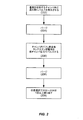
堆積されたタングステン膜およびタングステン前駆体中のフッ素(F)は、反応性の高いフッ化水素酸(HF)を形成する動作をさらに組み入れる過程で反応してよい。HFは、例えば酸化物スタック中の酸化物を侵食するか、あるいは組み入れに負の影響を及ぼすことがある。六フッ化タングステン(WF6)などのフッ素化前駆体を使用する、タングステン核形成層を堆積する従来の方法では、核形成層にある程度のフッ素が生じる。図2は、タングステン核形成層を堆積させる方法の一例における特定の動作を示すプロセスの流れ図である。図2を参照して説明する本方法では、フッ素含有量が低いタングステン核形成層が生じる。 Fluorine (F) in the deposited tungsten film and the tungsten precursor may react in the process of further incorporating the action of forming highly reactive hydrofluoric acid (HF). HF can erode oxides in the oxide stack, for example, or have a negative effect on inclusion. The conventional method of depositing a tungsten cambium using a fluorinated precursor such as tungsten hexafluoride (WF 6) produces some fluorine in the cambium. FIG. 2 is a process flow diagram showing a specific operation in an example of a method of depositing a tungsten nucleation layer. The method described with reference to FIG. 2 produces a tungsten nucleation layer with a low fluorine content.
図2を参照して以下に説明する方法は、基板を還元剤とフッ素含有タングステン前駆体との交互のルスに曝露することを必要とする。様々な実施形態によれば、この交互のパルスに曝露することは、時間的な切り替えまたは空間的な切り替えを必要としてよい。時間的な切り替えは、基板がチャンバなどの特定の環境で静止したままである場合に実施されてよい。空間的な切り替えは、基板を異なる環境に移動させることを必要としてよい。以下の説明は主に時間的な切り替えに言及しているが(よって、基板は、堆積中に特定のチャンバ環境にとどまっていると仮定する)、本方法を空間的な切り替えで実施することもできることが理解される。 The method described below with reference to FIG. 2 requires exposing the substrate to an alternating ruth of reducing agent and fluorine-containing tungsten precursor. According to various embodiments, exposure to this alternating pulse may require temporal or spatial switching. Temporal switching may be performed if the substrate remains stationary in a particular environment, such as a chamber. Spatial switching may require moving the substrate to a different environment. Although the following description mainly refers to temporal switching (hence the assumption that the substrate remains in a particular chamber environment during deposition), the method can also be implemented with spatial switching. It is understood that it can be done.
ブロック202でプロセスは、ウエハまたはその他の基板を収容するチャンバ内で還元剤にパルスすることを必要とする。還元剤は、タングステン前駆体を還元して(かつ/または還元できる分解生成物を形成して)タングステン(W)を形成できる化合物である。還元剤は、水素(H2)よりも強力な還元剤であってよく、その例には、シランなどのシリコン含有還元剤、ボランなどのホウ素含有還元剤、およびゲルマンなどのゲルマニウム還元剤がある。具体的な例には、シラン(SiH4)、ジシラン(Si2H6)、ボラン(BH3)、ジボラン(B2H6)、ゲルマン(GeH4)およびジゲルマン(Ge2H6)がある。ヒドラジンなどのその他の還元剤を用いてもよい。実施形態によっては、還元剤またはその分解生成物は、吸収されてもよいし、あるいは基板面の上に堆積されて反応に利用可能であってもよい。ブロック204では、基板面に堆積されない余分な還元剤がチャンバからパージされる。実施形態によっては、パージ動作が実施されなくてもよい。
At
ブロック206では、WF6などのフッ素含有タングステン前駆体が、基板を収容しているチャンバ内でパルスされ、チャンバは、パルス中は低チャンバ圧力である。低圧力は10トル未満である。実施形態によっては、圧力は7トル未満、5トル未満、または3トル未満である。
At
図2の例では、基板は、プロセス過程で単一のチャンバにとどまっている。このように、チャンバは、図2のどの動作過程でも低圧力であってよい。実施形態によっては、チャンバ圧力は、プロセス過程で実質的に一定である。当業者は、実質的に一定のチャンバ圧力には、異なるガス流が導入されるなどの理由で揺動が少ないチャンバ圧力が含まれることを理解するであろう。ただし、実施形態によっては、チャンバ圧力がブロック202でブロック206よりも高くなることがある。フッ素含有タングステン前駆体は、還元剤または分解生成物と反応してタングステン膜の層またはサブ層を形成する。以下にさらに詳細に説明するように、ブロック206を低圧で実施することによって、膜の中に組み込まれるフッ素の量は著しく減少する。ブロック202〜206は、所望の厚みのタングステンを形成するために、任意選択で1回以上繰り返されてよい。ブロック208。図2に描いたプロセスには様々な修正を加えてよい。実施形態によっては、例えば、ブロック206は、フッ素含有タングステン前駆体を還元剤のパルスよりも前にパルスしてもよいように、ブロック202よりも前に実施されてもよい。このように、フッ素含有前駆体またはその分解生成物は、還元剤の入力パルスと反応するために利用可能な基板上で吸収されてよい。
In the example of FIG. 2, the substrate remains in a single chamber during the process. Thus, the chamber may be under low pressure during any of the operating processes of FIG. In some embodiments, the chamber pressure is substantially constant during the process. Those skilled in the art will appreciate that a substantially constant chamber pressure includes a chamber pressure with less oscillation, such as due to the introduction of different gas streams. However, in some embodiments, the chamber pressure may be higher in
図3は、タングステン(W)/窒化チタンTiN/非ドープシリコンガラス(USG)のスタックに対するフッ素(F)濃度のプロフィールを示すグラフであり、ALDによって3トル、10トルおよび40トルでそれぞれ堆積されたW層を含むスタックに対するプロフィールを示している。六フッ化タングステンおよびジボランをそれぞれタングステン前駆体および還元剤として使用した。各プロフィールは、深さ約275Åまでの部分が比較的平坦で、続いてW/TiNインターフェースの所でF濃度が上昇し、TiN/USGインターフェースおよびUSG層で深さが増すにつれて低下していることが特徴的である。W層に示された上昇は、測定プロセスのアーチファクトであり、TiN層中のF含有量を反映していると思われる。このように、W層中のF含有量は、プロフィールの平坦部分で最もよく示されている。 FIG. 3 is a graph showing the profile of the fluorine (F) concentration relative to the stack of tungsten (W) / titanium nitride TiN / non-doped silicon glass (USG), deposited by ALD in 3 tol, 10 toll and 40 toll, respectively. The profile for the stack including the W layer is shown. Tungsten hexafluoride and diborane were used as the tungsten precursor and reducing agent, respectively. Each profile is relatively flat up to a depth of about 275 Å, followed by an increase in F concentration at the W / TiN interface and a decrease as the depth increases at the TiN / USG interface and the USG layer. Is characteristic. The rise shown in the W layer is an artifact of the measurement process and appears to reflect the F content in the TiN layer. Thus, the F content in the W layer is best shown in the flat portion of the profile.
当然ながら、10トルの膜(線304)は、40トルの膜(線306)よりもフッ素含有量が大幅に少ないが、10トル未満で堆積されたALD膜(線302)は、10トル(線304)および40トル(線306)で堆積された膜と比較してフッ素含有量が100分の1未満に減少している。線302の平坦部分は、1017原子/cm3で、フッ素を測定するのに使用した道具の検出レベルを下回っており、これは、フッ素レベルが1017原子/cm3よりも低い可能性があることを示している。この測定レベルは、フッ素を含まない前駆体を使用して堆積したタングステンにも相当し、これは、フッ素含有前駆体を用いて本質的にフッ素を含まないタングステン核形成層を堆積するために低圧(<10トル)プロセスを用いてよいことを示している。
Of course, a 10 toll membrane (line 304) has a significantly lower fluorine content than a 40 toll membrane (line 306), but an ALD membrane (line 302) deposited in less than 10 tolls has 10 tolls (line 302). The fluorine content is reduced to less than one-hundredth as compared to the membranes deposited on lines 304) and 40 tolls (line 306). The flat portion of
低圧プロセスは、実施形態によっては、下地誘電層でフッ素の量も減少させる。図4は、タングステンW/TiN/熱酸化物に対するフッ素F濃度のプロフィールを示しているグラフであり、WはALDによって薄い(30Å)TiNバリア層に堆積されている。300ÅのW核形成/30ÅのTiN/1000Åの熱酸化物の3スタックのプロフィールを示しており、300ÅのWタングステン核形成層は、3トル、10トルおよび40トルのそれぞれで堆積されている。ここで、3トルのW層中のF濃度は、(図3のように)F検出レベルを下回っている。さらに、圧力が下がると、熱酸化物層中のF濃度が低くなっている。 The low pressure process also reduces the amount of fluorine in the underlying dielectric layer, depending on the embodiment. FIG. 4 is a graph showing the profile of fluorine F concentration relative to tungsten W / TiN / thermal oxide, where W is deposited in a thin (30 Å) TiN barrier layer by ALD. It shows the profile of 3 stacks of 300 Å W nucleation / 30 Å TiN / 1000 Å thermal oxide, with 300 Å W tungsten nucleation layers deposited in 3 tor, 10 tor and 40 tor, respectively. Here, the F concentration in the W layer of 3 torr is below the F detection level (as shown in FIG. 3). Further, as the pressure decreases, the F concentration in the thermal oxide layer decreases.
前述したように、フッ素含有タングステン前駆体を用いてタングステン核形成層を低圧でALD堆積すると、フッ素を含まない前駆体を用いて、または固体タングステンの物理気相堆積(PVD)によって堆積した膜と対等のフッ素含有量になる。図5は、W/TiN/熱酸化物のスタックに対するF濃度のプロフィールを示しているグラフである。プロフィールは、以下のW堆積方法を示している:WF6を用いて40トルでALD(線506)、WF6を用いて10トルでALD(線504)、WF6を用いて3トルでALD(線502)、フッ素を含まないタングステン(FFW)前駆体を用いて40トルでALD(線505)、およびPVD(線503)。 As mentioned above, ALD deposition of a tungsten nucleation layer at low pressure using a fluorine-containing tungsten precursor results in a film deposited using a fluorine-free precursor or by physical vapor deposition (PVD) of solid tungsten. Equal fluorine content. FIG. 5 is a graph showing a profile of F concentration relative to a stack of W / TiN / thermal oxides. Profile shows the following W deposition process: ALD at 40 torr using a WF 6 (line 506), ALD at 10 torr using a WF 6 (line 504), ALD at 3 Torr using WF 6 (Line 502), ALD (Line 505), and PVD (Line 503) at 40 tons using a fluorine-free tungsten (FFW) precursor.
図5は、WのALD膜のバルク中にあるFの割合が40トルのALDプロセスで最も多く、10トルのALDプロセスがそれに続いていることを示している。10トルのALD膜中にあるF含有量は、FFW膜中のF含有量とほぼ等しい。F含有量は、3トルのALDおよびPVD膜で最も低い。当然ながら、3トルのWF6膜で測定したFはFFW膜よりも少ない。 FIG. 5 shows that the proportion of F in the bulk of W's ALD membrane is highest in the 40 torr ALD process, followed by the 10 torr ALD process. The F content in 10 torr of ALD membrane is approximately equal to the F content in FFW membrane. The F content is lowest in 3 torr of ALD and PVD membranes. As a matter of course, the F measured with the WF 6 membrane of 3 torr is less than that of the FFW membrane.
TiN/酸化物のインターフェースでは、F含有量は、40トルのALD膜で最も高く、これに10トルのALD膜、3トルのALD膜、ならびにFFWおよびPVD膜が(順に)続く。 In the TiN / oxide interface, the F content is highest in 40 torr ALD membranes, followed by 10 torr ALD membranes, 3 torr ALD membranes, and (in order) FFW and PVD membranes.
図3〜5に見られるフッ素含有量とチャンバ圧力との非線形的な相関関係は、予想外であった。なぜなら、WF6系のALDで堆積した膜中のフッ素は一般に、温度などの他のプロセスパラメータの変化にはほとんど反応しないからというのがその理由の一部である。基板の温度を上昇させることで、フッ素含有量をある程度減少させることができるが、FFW膜のフッ素含有量に近づけるには十分ではない。さらに、温度が上昇すると、ステップカバレッジが縮小してしまう。これとは対照的に、本明細書に開示した低圧プロセスでは、良好なステップカバレッジ(例えば少なくとも90%)を得ることができる。フッ素系のタングステン前駆体を用いるCVD堆積は、図3〜5に示したようにチャンバ圧力に反応しないことにも注意されたい。特定の理論に拘束されるものではないが、ALDプロセス過程での低チャンバ圧力で、フッ素(F2)または反応から生じるその他のF含有副生成物をW膜から拡散させるか、またはW膜の表面を堆積された通りに残すことが可能になってよいと思われる。 The non-linear correlation between the fluorine content and the chamber pressure seen in FIGS. 3-5 was unexpected. Part of the reason is that fluorine in WF 6 ALD-deposited membranes generally has little reaction to changes in other process parameters such as temperature. By raising the temperature of the substrate, the fluorine content can be reduced to some extent, but it is not sufficient to approach the fluorine content of the FFW film. Furthermore, as the temperature rises, the step coverage shrinks. In contrast, the low pressure processes disclosed herein can provide good step coverage (eg at least 90%). It should also be noted that CVD deposition using a fluorinated tungsten precursor does not respond to chamber pressure as shown in FIGS. 3-5. Without being bound by a particular theory, at low chamber pressures during the ALD process, fluorine (F 2 ) or other F-containing by-products resulting from the reaction can be diffused from the W membrane or of the W membrane. It would be possible to leave the surface as it was deposited.
図2のプロセスでは、反応体をチャンバに供給するのにキャリアガスを使用してよい。使用した場合、キャリアガスの流速は通常、チャンバ圧力がキャリアガスの分圧に近づいてよいように反応体よりも遙かに速い。キャリアガスは、反応体のパルスの間でパージガスとして機能してもよいし、あるいは別のパージガスを使用してもよい。アルゴン、キセノン、クリプトン、窒素、またはヘリウムなどの不活性成分をキャリアガスとして使用してもよい。 In the process of FIG. 2, carrier gas may be used to feed the reactants to the chamber. When used, the carrier gas flow rate is usually much faster than the reactants so that the chamber pressure may approach the partial pressure of the carrier gas. The carrier gas may function as a purge gas during the pulse of the reactants, or another purge gas may be used. Inactive components such as argon, xenon, krypton, nitrogen, or helium may be used as the carrier gas.
様々な実施形態によれば、別のキャリアガスに加えて、またはその代わりに水素をバックグラウンドで流してもよいし流さなくてもよい。実施形態によってはバックグラウンドで水素を流さず、それによって核形成層堆積は水素(H2)のないプロセスになる。H2を添加すると、おそらくHFの生成によりフッ素の減少を向上させることができる。 According to various embodiments, hydrogen may or may not flow in the background in addition to or instead of another carrier gas. In some embodiments, hydrogen does not flow in the background, which makes cambium deposition a hydrogen (H 2 ) -free process. The addition of H 2 can improve the reduction of fluorine, probably by the formation of HF.
フッ素汚染の有害な作用を防止することに加えて、低圧プロセスで抵抗率を低下させることができる。図6は、40トルのALDプロセス(バックグラウンドでH2あり)およびH2なしの3トルのALDプロセスに対する抵抗率の測定値を示している。WF6を、タングステン含有前駆体として使用し、B2H6を還元剤として使用した。抵抗率は低圧プロセスで著しく低下しており、これは、膜中のF不純物の量が減少したことが原因であってよい。図6のデータ生成時に堆積された膜は非晶質で、3トルの膜の抵抗率が非晶質膜にしては極めて低かったことに注意されたい。 In addition to preventing the harmful effects of fluorine contamination, resistivity can be reduced in low pressure processes. FIG. 6 shows measurements of resistivity to a 40 torr ALD process (with H 2 in the background) and a 3 torr ALD process without H 2. WF 6 was used as the tungsten-containing precursor and B 2 H 6 was used as the reducing agent. The resistivity is significantly reduced in the low pressure process, which may be due to the reduced amount of F impurities in the membrane. It should be noted that the film deposited at the time of data generation in FIG. 6 was amorphous, and the resistivity of the 3-torr film was extremely low for an amorphous film.
図3〜6のデータを生成するのに使用した3トルのALD堆積は、10トルおよび40トルで堆積するのに使用する道具に限りがあるため、10トルおよび40トルのALD堆積とは異なる道具で実施されたことに注意されたい。 The 3-toll ALD deposit used to generate the data in FIGS. 3-6 differs from the 10-toll and 40-toll ALD deposits due to the limited tools used to deposit at 10 and 40 tolls. Note that it was done with tools.
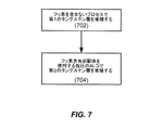
実施形態によっては、フッ素含有タングステン前駆体を使用して低圧でALDによってタングステン層を堆積させる前に、フッ素を含まないプロセスで第1のタングステン層を堆積させてよい。このようなプロセスは、例えば、下地層内または層間のインターフェースでフッ素含有量を減少させるのに有用としてよい。図7は、タングステンを堆積する方法の一例における特定の動作を示すプロセスの流れ図である。本方法は、フッ素を含まないプロセスで第1のタングステン層を堆積する(702)ことを含む。第1のタングステン層は、例えば、チタン(Ti)、TiN、Ti/TiN、窒化タングステン(WN)などのバリア層もしくは接着層、またはその他の層に堆積されてよい。実施形態によっては、第1のタングステンは、酸化シリコン層などの誘電層に直接堆積されてよい。 In some embodiments, the first tungsten layer may be deposited in a fluorine-free process prior to depositing the tungsten layer by ALD at low pressure using the fluorine-containing tungsten precursor. Such a process may be useful, for example, in reducing the fluorine content within or at the interface between layers. FIG. 7 is a process flow diagram showing a specific operation in an example of a method of depositing tungsten. The method comprises depositing a first tungsten layer (702) in a fluorine-free process. The first tungsten layer may be deposited on a barrier layer or an adhesive layer such as titanium (Ti), TiN, Ti / TiN, tungsten nitride (WN), or another layer. In some embodiments, the first tungsten may be deposited directly on a dielectric layer such as a silicon oxide layer.
非フッ素プロセスの例には、フッ素含有前駆体を使用しないALDおよびCVDプロセスなどがある。使用されてよいフッ素を含まないタングステン前駆体の例には、タングステンヘキサカルボニル(W(CO)6)、六塩化タングステン(WCl6)および五塩化タングステン(WCl5)などのタングステン塩化物、ならびにW2(NMe2)6、W(OEt)6、W(OnPr)6、(tBuN=)2W(NMe2)2、(tBuN )2W(NEtMe)2、W(Cp)2H2、W(NEt2)2(NEt)2、W(iPrCp)2H2、(tBuN=)2W(HNMe)2、W(EtCp)2H2およびこれらの誘導体などの有機タングステンの前駆体がある。さらに他の例には、Praxair社が販売するエチルシクロペンタジエニル−ジカルボニルニトロシル−タングステン(EDNOW)、メチルシクロペンタジエニル−ジカルボニルニトロシル−タングステン(MDNOW)、およびエチルシクロペンタジエニル−トリカルボニル水素化タングステン(ETHW)、ならびに、下記の構造を有すウルタングステンビス(アルキルイミノ)ビス(アルキルアミノ)化合物がある。

第1のタングステン層は、後続の堆積でフッ素含有タングステンプロセスから生じたフッ素が下地材料に達するのを防ぐのに十分な厚みになるように堆積されてよい。厚み範囲の例は、10Å〜100Åであってよいが、この範囲以外の厚みを実現してもよい。 The first tungsten layer may be deposited to a thickness sufficient to prevent the fluorine generated from the fluorine-containing tungsten process from reaching the underlying material in subsequent deposition. An example of the thickness range may be 10 Å to 100 Å, but a thickness other than this range may be realized.
本方法は続いて、フッ素含有前駆体を使用する低圧のALDで第2のタングステン層を堆積する。ブロック704。第2のタングステン層は、第1のタングステン層に直接堆積されたタングステン核形成層であってよい。ブロック704は、図2に関して前述したプロセスを必要としてもよい。
The method subsequently deposits a second tungsten layer with a low pressure ALD using a fluorine-containing precursor.
ブロック704の堆積速度は、ブロック702よりも遙かに速くてよい。このように、ブロック702では、下地層をフッ素から保護するフッ素を含まない層になってよく、ブロック704では、極めて少ないフッ素含有量でより速い堆積になる。
The deposition rate of
実施形態によっては、タングステン核形成層の堆積に続いて、1つ以上の処理動作を行ってからタングステンのバルク堆積を行ってもよい。堆積したタングステン核形成層をより低い抵抗率で処理することが、例えば米国特許第7,772,114号および第8,058,170号および米国特許公報第2010−0267235号に記載され、これらを参照することにより本願に援用する。 Depending on the embodiment, one or more treatment operations may be performed following the deposition of the tungsten nucleation layer, and then the bulk deposition of tungsten may be performed. Treating the deposited tungsten nucleating layer with a lower resistivity is described, for example, in US Pat. Nos. 7,772,114 and 8,058,170 and US Pat. No. 2010-0267235, which are described. Incorporated into this application by reference.
タングステン層の低圧でのALD堆積に続いて、タングステンのバルク堆積を行ってよい。タングステンのバルク堆積はCVDプロセスで実行でき、このプロセスでは、還元剤およびタングステン含有前駆体が堆積チャンバに流れ込んで特徴部にバルク充填層を堆積する。反応体の流束を1つ以上供給するために不活性キャリアガスを使用してよく、この流束は、事前に混合されていてもいなくてもよい。PNLまたはALDプロセスとは異なり、CVDの動作は一般に、反応体を所望量が堆積されるまで連続的に一緒に流すことを必要とする。特定の実施形態では、CVDの動作は、複数の段階で、反応体が連続的かつ同時に流れる複数の期間がある状態で、この期間が、1つ以上の反応体が反れて流れる期間で分離されている状態で行われてよい。 ALD deposition at low pressure in the tungsten layer may be followed by bulk deposition of tungsten. Bulk deposition of tungsten can be performed in a CVD process, in which the reducing agent and the tungsten-containing precursor flow into the deposition chamber to deposit the bulk packed bed in the features. An inert carrier gas may be used to supply one or more fluxes of the reactants, which may or may not be premixed. Unlike the PNL or ALD process, the operation of CVD generally requires the reactants to be continuously flowed together until the desired amount is deposited. In certain embodiments, the CVD operation is divided into multiple stages, with multiple periods in which the reactants flow continuously and simultaneously, with these periods separated by periods in which one or more reactants flow in a warped manner. It may be done in the state of being.
上記に列挙したWF6、WCl6、WCl5、W(CO)6または有機タングステン前駆体などだがこれに限定されない様々なタングステン含有ガスを、タングステン含有前駆体として使用できる。特定の実施形態では、タングステン含有前駆体は、WF6などのハロゲン含有化合物である。特定の実施形態では、還元剤は水素ガスだが、他の還元剤を使用してもよく、それにはシラン(SiH4)、ジシラン(Si2H6)ヒドラジン(N2H4)、ジボラン(B2H6)およびゲルマン(GeH4)などがある。多くの実施形態では、CVDプロセスで水素ガスガスが還元剤として使用される。その他の実施形態によっては、バルクタングステン層を形成するために分解できるタングステン前駆体を使用できる。バルク堆積は、ALDプロセスなどの他の種類のプロセスを用いて行われてもよい。引き続きさらに、バルク堆積は、連続したCVDプロセスを用いて行われてよい。このようなプロセスの説明が、同時出願された米国特許出願(代理人整理番号LAMRP184/3601)に記載されている。温度範囲の例は200℃〜500℃であってよい。様々な実施形態によれば、本明細書に記載したCVDのW動作のいずれも、例えば約250℃〜350℃または約300℃などの低温でのCVDのW充填を用いることができる。 Various tungsten-containing gases such as, but not limited to , WF 6 , WCl 6 , WCl 5 , W (CO) 6 or organic tungsten precursors listed above can be used as the tungsten-containing precursors. In certain embodiments, the tungsten-containing precursor is a halogen-containing compound such as WF 6. In certain embodiments, the reducing agent is hydrogen gas, but other reducing agents may be used, such as silane (SiH 4 ), disilane (Si 2 H 6 ) hydrazine (N 2 H 4 ), diborane (B). 2 H 6) and germane (GeH 4), and the like. In many embodiments, hydrogen gas is used as the reducing agent in the CVD process. In some other embodiments, a degradable tungsten precursor can be used to form the bulk tungsten layer. Bulk deposition may be performed using other types of processes such as the ALD process. Subsequently, further bulk deposition may be performed using a continuous CVD process. A description of such a process is described in the co-filed US patent application (agent reference number LAMRP184 / 3601). An example of the temperature range may be 200 ° C to 500 ° C. According to various embodiments, any of the CVD W operations described herein can use CVD W filling at low temperatures, such as, for example, about 250 ° C to 350 ° C or about 300 ° C.
堆積は、様々な実施形態によれば、特定の特徴部の輪郭が達成され、かつ/または特定量のタングステンが堆積されるまで進行してよい。実施形態によっては、堆積時間およびその他の関連パラメータは、モデリングおよび/または試行錯誤によって決定されてよい。例えば、ピンチオフになるまでタングステンを特徴部にコンフォーマルに堆積できるインサイドアウト式の充填プロセスで最初に堆積させる場合、特徴部の寸法に基づいて、ピンチオフを達成するタングステンの厚みおよびその堆積時間を決定することが率直なことがある。実施形態によっては、処理チャンバには、堆積動作のエンドポイントを検出するために、in−situ計測測定を実施する様々なセンサを備えてよい。in−situ計測の例には、堆積された膜の厚みを算出する光学顕微鏡法および蛍光X線(XRF)などがある。 Deposition may proceed until a particular feature contour is achieved and / or a particular amount of tungsten is deposited, according to various embodiments. Depending on the embodiment, the deposition time and other related parameters may be determined by modeling and / or trial and error. For example, if the first deposit is an inside-out filling process that allows the tungsten to be conformally deposited in the feature until pinch-off, the dimensions of the feature determine the thickness of the tungsten to achieve pinch-off and its deposition time. It can be frank to do. In some embodiments, the processing chamber may be equipped with various sensors that perform in-situ measurements to detect the endpoint of the deposition operation. Examples of in-situ measurements include optical microscopy and fluorescent X-ray (XRF) to calculate the thickness of the deposited film.
本明細書に記載したタングステン膜のいずれも、使用する特定の前駆体およびプロセスに応じて、他の化合物、ドーパントおよび/または窒素、炭素、酸素、ホウ素、リン、硫黄、シリコン、ゲルマニウムなどの不純物を含んでいてよいことを理解されたい。膜中のタングステン含有量の範囲は、20%〜100%の(原子)タングステンであってよい。多くの実施形態では、膜はタングステンが豊富で、少なくとも50%の(原子)タングステン、あるいは少なくとも約60%、75%、90%、または99%の(原子)タングステンを含んでいる。実施形態によっては、膜は、金属または元素状態のタングステン(W)と、炭化タングステン(WC)、窒化タングステン(WN)などのその他のタングステン含有化合物との混合物であってよい。 Any of the tungsten films described herein may contain other compounds, dopants and / or impurities such as nitrogen, carbon, oxygen, boron, phosphorus, sulfur, silicon, germanium, etc., depending on the particular precursor and process used. Please understand that it may include. The range of tungsten content in the membrane may be 20% to 100% (atomic) tungsten. In many embodiments, the membrane is rich in tungsten and contains at least 50% (atomic) tungsten, or at least about 60%, 75%, 90%, or 99% (atomic) tungsten. In some embodiments, the membrane may be a mixture of tungsten (W) in metallic or elemental state with other tungsten-containing compounds such as tungsten carbide (WC), tungsten nitride (WN).
これらの材料のCVD、ALDおよび低圧ALD堆積は、任意の適切な前駆体を使用することを含むことができる。例えば、窒化タングステンのCVDおよびALD堆積は、以下にさらに詳細に説明するように、ハロゲン含有化合物と、ハロゲンがなくタングステン含有かつ窒素含有の化合物とを使用することを含むことができる。チタン含有層のCVDおよびALD堆積は、チタンを含有する前駆体、例としてテトラキス(ジメチルアミノ)チタン(TDMAT)および塩化チタン(TiCl4)と、必要であれば1つ以上の共反応体とを使用することを含むことができる。タンタル含有層のCVDおよびALD堆積は、ペンタキス−ジメチルアミノタンタル(PDMAT)およびTaF5などの前駆体と、必要であれば1つ以上の共反応体とを使用することを含むことができる。コバルト含有層のCVDおよびALD堆積は、トリス(2,2,6,6−テトラメチル−3,5−ヘプタンジオナト)コバルト、ビス(シクロペンタジエニル)コバルト、およびジコバルトヘキサカルボニルブチルアセチレンなどの前駆体と、1つ以上の共反応体とを使用することを含むことができる。ニッケル含有層のCVDおよびALD堆積は、シクロペンタジエニルアリルニッケル(CpAllylNi)およびMeCp2Niなどの前駆体を使用することを含むことができる。共反応体の例には、N2、NH3、N2H4、N2H6、SiH4、Si3H6、B2H6、H2、およびAlCl3があり得る。本明細書に記載の方法は、フッ素含有前駆体を使用する様々な膜のALDに使用されてよい。
装置
CVD, ALD and low pressure ALD deposition of these materials can include the use of any suitable precursor. For example, CVD and ALD deposition of tungsten nitride can include the use of halogen-containing compounds and halogen-free, tungsten-containing and nitrogen-containing compounds, as described in more detail below. CVD and ALD deposition of titanium-containing layers involves titanium-containing precursors such as tetrakis (dimethylamino) titanium (TDMAT) and titanium chloride (TiCl 4 ) and, if necessary, one or more copolymers. Can include use. CVD and ALD deposition of tantalum-containing layers can include the use of precursors such as pentakis-dimethylaminotantalum (PDMAT) and TaF 5 and, if desired, one or more copolymers. CVD and ALD deposition of cobalt-containing layers are precursors such as Tris (2,2,6,6-tetramethyl-3,5-heptandionat) cobalt, bis (cyclopentadienyl) cobalt, and dicobalt hexacarbonylbutylbutylacetylene. The use of a body and one or more copolymers can be included. CVD and ALD deposition of the nickel-containing layer may include the use of a precursor such as a cyclopentadienyl-allyl nickel (CpAllylNi) and MeCp 2 Ni. Examples of reactants may be N 2 , NH 3 , N 2 H 4 , N 2 H 6 , Si H 4 , Si 3 H 6 , B 2 H 6 , H 2 , and AlCl 3 . The methods described herein may be used for ALD of various membranes using fluorine-containing precursors.
Device
開示した実施形態を実施するために、任意の適切なチャンバを使用してよい。例としての堆積装置には様々なシステムがあり、例えば、米国カリフォルニア州フリーモント市所在のLam Research Corp.,が販売しているALTUS(登録商標)およびALTUS(登録商標)Max、またはその他の多岐にわたる市販の処理システムがある。実施形態によっては、低圧ALDは、単一の堆積チャンバ内に設置された2つ、5つ、あるいはそれよりも多くの堆積ステーションのうちの1つであるステーションで実施されてよい。そのため、例えば、ジボランおよび六フッ化タングステンは、基板表面に局所的な雰囲気を生み出す別個のガス供給システムを使用して、ステーションで半導体基板の表面に交互に導入されてよい。フッ素を含まないタングステン堆積、またはCVDに対して別のステーションを使用してよい。並列処理でタングステンを堆積するために2つ以上のステーションを使用してよい。その代わりに、様々な動作を2つ以上のステーションにわたって順に実施させるためにウエハを割り出ししてよい。 Any suitable chamber may be used to carry out the disclosed embodiments. There are various systems of sedimentation equipment as an example, for example, Lam Research Corp. located in Fremont, California, USA. , Are sold by ALTUS® and ALTUS® Max, or a wide variety of other commercially available processing systems. In some embodiments, the low pressure ALD may be performed at a station that is one of two, five, or more deposition stations installed in a single deposition chamber. So, for example, diborane and tungsten hexafluoride may be alternately introduced to the surface of the semiconductor substrate at the station using a separate gas supply system that creates a local atmosphere on the substrate surface. Another station may be used for fluorine-free tungsten deposition or CVD. Two or more stations may be used to deposit tungsten in parallel processing. Alternatively, wafers may be indexed to sequentially perform various operations across two or more stations.
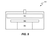
図8は、実施形態に従ってタングステン薄膜を堆積させるプロセスを実行するのに適している処理システムのブロック図である。システム800は、搬送モジュール803を備えている。搬送モジュール803は、様々な反応モジュールどうしの間を移動するため、清潔な加圧環境を提供して処理されている基板が汚染されるリスクを最小に抑える。搬送モジュール803に取り付けられているのは、実施形態によるALDおよびCVDを実施する能力があるマルチステーション反応装置809である。マルチステーション反応装置809は、実施形態によっては、低圧でのタングステンALDおよび/またはタングステンCVDを実施するのに使用されてもよい。マルチステーション反応装置809は、開示した実施形態による動作を順に実施してよい複数のステーション811、813、815、および817を備えていてよい。例えば、マルチステーション反応装置809は、ステーション811がALDによるフッ素を含まない核形成層の堆積を実施し、ステーション813が低圧ALDを実施し、ステーション815および817がCVDを実施するように構成されることが可能である。ステーションは、加熱された基台もしくは基板支持体、1つ以上のガス入口もしくはシャワーヘッドまたは散布プレートを備えていてよい。基板支持体902およびシャワーヘッド903を備えている堆積ステーション900の一例を図9に示している。基台部分901にヒータを設けてよい。基台901は、ウエハを固定するためのチャックを備えていてよい。特定の実施形態では、低圧環境を用意しやすくするために、真空チャックよりも静電チャックまたは機械チャックを用いてよい。ガスは、排気管(図示せず)を介して堆積ステーション900の外へ排出されてよい。
FIG. 8 is a block diagram of a processing system suitable for performing the process of depositing a tungsten thin film according to an embodiment. The
また、搬送モジュール803には、プラズマまたは化学的な(プラズマではない)プレクリーンを実施する能力がある1つ以上の単一ステーションモジュールまたはマルチステーションモジュール807を取り付けてもよい。モジュールは、例えば堆積プロセス用に基板を準備するための様々な処理に使用されてもよい。システム800は、1つ以上のウエハ供給源モジュール801も備え、このモジュールにウエハが処理前後に格納される。空気搬送チャンバ819にある空気ロボット(図示せず)が、まずウエハを供給源モジュール801からロードロック821に移動させてよい。搬送モジュール803にあるウエハ搬送装置(一般にはロボットアームユニット)が、ウエハをロードロック821から搬送モジュール803に取り付けられたモジュールに移動させ、かつ同モジュールの中に移動させる。
The
様々な実施形態では、堆積過程でプロセスの条件を制御するためにシステムコントローラ829が用いられる。コントローラ829は通常、1つ以上の記憶装置および1つ以上のプロセッサを備える。Aプロセッサは、CPUまたはコンピュータ、アナログおよび/またはデジタル入力/出力接続部、ステッパモータの制御盤などを備えていてよい。
In various embodiments, a
コントローラ829は、堆積装置の全動作を制御してよい。システムコントローラ829は、タイミング、ガスの混合、チャンバの圧力、チャンバの温度、ウエハの温度、ウエハのチャックまたは基台の位置、および特定のプロセスの他のパラメータを制御する命令セットを含んでいるシステム制御ソフトウェアを実行する。実施形態によっては、コントローラ829に接続している記憶装置に格納されたその他のコンピュータプログラムを用いてよい。
The
通常は、コントローラ829に接続しているユーザインターフェースがある。ユーザインターフェースは、表示画面、装置のグラフィックソフトウェアディスプレイおよび/またはプロセス条件、ならびにポインティングデバイス、キーボード、タッチ画面、マイクロフォンなどのユーザ入力デバイスを備えていてよい。
Usually, there is a user interface connected to the
システム制御ロジックは、任意の適切な方法で構成されてよい。一般に、ロジックは、ハードウェアおよび/またはソフトウェアに設計または構成され得る。ドライブ回路を制御するための命令は、ハードコードされてもよいし、ソフトウェアとして提供されてもよい。命令は、「プログラミング」によって提供されてよい。このようなプログラミングは、デジタルシグナルプロセッサ、特定用途集積回路、およびハードウェアとして実装された特別なアルゴリズムを有するその他のデバイスにハードコードされたロジックなど、任意の形態のロジックを含むことが理解される。プログラミングは、汎用プロセッサ上で実行されてよいソフトウェアまたはファームウェアの命令を含むことも理解される。システム制御ソフトウェアは、任意の適切なコンピュータ可読プログラミング言語でコード化されてよい。 The system control logic may be configured in any suitable way. In general, logic can be designed or configured in hardware and / or software. Instructions for controlling the drive circuit may be hard-coded or provided as software. Instructions may be provided by "programming". It is understood that such programming includes any form of logic, such as digital signal processors, application-specific integrated circuits, and logic hard-coded into other devices with special algorithms implemented as hardware. .. It is also understood that programming includes software or firmware instructions that may be executed on a general purpose processor. The system control software may be encoded in any suitable computer-readable programming language.
ゲルマニウム含有還元剤のパルス、水素の流れ、およびタングステン含有前駆体のパルス、ならびに一連のプロセスにあるその他のプロセスを制御するためのコンピュータプログラムコードは、任意の従来のコンピュータ可読プログラミング言語、例えばアセンブリ言語、C、C++、Pascal、Fまたはtranなどで記述され得る。プログラムで識別されたタスクを実施するために、コンパイルされたオブジェクトコードまたはスクリプトがプロセッサによって実行される。また、前述したように、プログラムコードはハードコードされてよい。 Computer program code for controlling germanium-containing reducing agent pulses, hydrogen flow, and tungsten-containing precursor pulses, as well as other processes in a series of processes, can be written in any conventional computer-readable programming language, such as assembly language. , C, C ++, Pascal, F or tran and the like. Compiled object code or scripts are executed by the processor to perform the tasks identified by the program. Also, as mentioned above, the program code may be hard-coded.
コントローラのパラメータは、プロセスの条件、例えば、処理ガスの組成および流速、温度、圧力、冷却ガスの圧力、基板の温度、ならびにチャンバの壁の温度などに関連している。これらのパラメータは、レシピの形態でユーザに提供されており、ユーザインターフェースを用いて入力されてよい。 Controller parameters are related to process conditions such as processing gas composition and flow rate, temperature, pressure, cooling gas pressure, substrate temperature, and chamber wall temperature. These parameters are provided to the user in the form of a recipe and may be entered using the user interface.
プロセスを監視する信号が、システムコントローラ829のアナログおよび/またはデジタル入力接続部を介して提供されてよい。プロセスを制御するための信号は、システム800のアナログおよびデジタル出力接続部に出力される。
Signals to monitor the process may be provided via the analog and / or digital input connections of the
システムソフトウェアは、多くの異なる方法で設計または構成されてよい。例えば、様々なチャンバ構成要素のサブルーチンまたは制御オブジェクトは、開示した実施形態に従って堆積プロセスを実行するのに必要なチャンバ構成要素の動作を制御するために記述されてよい。そのためのプログラムまたはプログラムの一部の例には、基板位置決めコード、処理ガス制御コード、圧力制御コード、およびヒータ制御コードがある。 System software may be designed or configured in many different ways. For example, various chamber component subroutines or control objects may be described to control the operation of the chamber components required to perform the deposition process according to the disclosed embodiments. Examples of the program or part of the program for this include a substrate positioning code, a processing gas control code, a pressure control code, and a heater control code.
実施形態によっては、コントローラ829はシステムの一部であり、このシステムは、前述した例の一部であってよい。このようなシステムは、半導体処理設備を備えることができ、これには、処理用の1つまたは複数の処理ツール、1つまたは複数のチャンバ、1つまたは複数のプラットフォーム、および/または特定の処理用構成要素(ウエハの基台、ガス流システムなど)がある。これらのシステムは、半導体のウエハまたは基板を処理する前、その最中および後に動作を制御するための電子機器と一体化していてよい。電子機器は、「コントローラ」と呼んでよく、このコントローラは、1つまたは複数のシステムの様々な構成要素またはサブ部分を制御してよい。コントローラ829は、処理要件および/またはシステムの種類に応じて、本明細書に開示した任意のプロセスを制御するようにプログラムされてよく、それには、処理ガスの供給、温度設定(例えば加熱および/または冷却)、圧力設定、真空設定、電力設定、流束設定、流体供給設定、位置決めおよび動作の設定、ツールおよびその他の搬送機へのウエハの搬送およびそこからの搬出、ならびに/または特定のシステムに接続しているか、同システムとインターフェースで接続しているロードロックがある。
In some embodiments, the
概して、コントローラは、様々な集積回路、ロジック、メモリ、および/または命令を受け取り、命令を出し、動作を制御し、洗浄動作を可能にし、エンドポイント測定を可能にするソフトウェアなどを有する電子機器であると定義されてよい。集積回路は、プログラム命令を格納するファームウェア形態のチップ、デジタルシグナルプロセッサ(DSP)、特定用途向け集積回路(ASIC)と定義されたチップ、および/または1つ以上のマイクロプロセッサ、またはプログラム命令(例えばソフトウェア)を実行するマイクロコントローラを備えていてよい。プログラム命令は、様々な個別設定(またはプログラムファイル)の形態でコントローラに通信される命令であってよく、半導体ウエハ上で、もしくは半導体ウエハに対して、またはシステムに対して特定のプロセスを実行するための動作パラメータを規定する。動作パラメータは、実施形態によっては、1つ以上の層、材料、金属、酸化物、シリコン、二酸化シリコン、表面、回路、および/またはウエハのダイの製造過程で1つ以上の処理工程を達成するために、プロセスのエンジニアが規定するレシピの一部であってよい。 In general, a controller is an electronic device that has various integrated circuits, logic, memory, and / or software that receives instructions, issues instructions, controls operations, enables cleaning operations, enables endpoint measurements, and so on. May be defined as being. An integrated circuit is a chip in the form of firmware that stores program instructions, a digital signal processor (DSP), a chip defined as an application specific integrated circuit (ASIC), and / or one or more microprocessors, or program instructions (eg, an integrated circuit). It may be equipped with a microcontroller that runs the software). A program instruction may be an instruction that is communicated to the controller in the form of various individual settings (or program files) and executes a specific process on or to the semiconductor wafer or to the system. Specifies the operating parameters for. The operating parameters, in some embodiments, achieve one or more processing steps in the process of manufacturing one or more layers, materials, metals, oxides, silicon, silicon dioxide, surfaces, circuits, and / or wafer dies. Therefore, it may be part of a recipe specified by the engineer of the process.
コントローラ829は、実施形態によっては、システムと一体化して同システムに連結しているか、そうでなければシステムにネットワークで接続しているか、これらの組み合わせであるコンピュータの一部であってもよいし、同コンピュータに連結していてもよい。例えば、コントローラ829は、「クラウド」にあってもよいし、工場ホストコンピュータシステムの全体または一部にあってもよく、これによって、ウエハの処理へのリモートアクセスが可能になり得る。コンピュータは、システムへのリモートアクセスを可能にして、現在の製造動作の進捗を監視したり、過去の製造動作の履歴を調べたり、複数の製造動作から傾向または性能の指標を調べたり、現在の処理のパラメータを変更したり、現在の処理に続く処理工程を設定したり、新たなプロセスを開始したりしてよい。いくつかの例では、リモートコンピュータ(例えばサーバ)が、プロセスのレシピをネットワーク上でシステムに提供でき、このネットワークには、ローカルネットワークまたはインターネットがあってよい。リモートコンピュータは、パラメータおよび/または設定の入力またはプログラミングを可能にするユーザインターフェースを備えていてよく、このパラメータおよび/または設定はその後、リモートコンピュータからシステムに通信される。いくつかの例では、コントローラは、データの形態で命令を受け取り、この命令は、1つ以上の動作過程で実施される処理工程の各々に対してパラメータを指定する。パラメータは、実施されるプロセスの種類、および、コントローラがインターフェースで接続されるか制御するように構成されているツールの種類に特有のものであってよいことを理解されたい。そのため、前述したように、一緒にネットワーク接続され、本明細書に記載のプロセスおよび制御などの共通の目的に向けて機能する1つ以上の別々のコントローラを備えることなどによって、コントローラは分配されてよい。このような目的のために分配されたコントローラの一例が、チャンバにある1つ以上の集積回路が、(例えばプラットフォームレベルで、またはリモートコンピュータの一部として)チャンバでのプロセスを制御するために協働する遠隔に位置している1つ以上の集積回路と通信している例である。
Depending on the embodiment, the
非限定的に、例としてのシステムには、プラズマエッチングチャンバまたはモジュール、堆積チャンバまたはモジュール、スピンリンスチャンバまたはモジュール、金属めっきチャンバまたはモジュール、洗浄チャンバまたはモジュール、ベベルエッジエッチングチャンバまたはモジュール、PVDチャンバまたはモジュール、CVDチャンバまたはモジュール、ALDチャンバまたはモジュール、原子層エッチング(ALE)チャンバまたはモジュール、イオン注入チャンバまたはモジュール、トラックチャンバまたはモジュール、ならびに、半導体ウエハの製造および/または生産に関連するか使用されてよい任意のその他の半導体処理システムがあってよい。 Non-limiting examples include plasma etching chambers or modules, deposition chambers or modules, spin rinse chambers or modules, metal plating chambers or modules, cleaning chambers or modules, bevel edge etching chambers or modules, PVD chambers or Related to or used in the manufacture and / or production of modules, CVD chambers or modules, ALD chambers or modules, atomic layer etching (ALE) chambers or modules, ion injection chambers or modules, track chambers or modules, and semiconductor wafers. There may be any other semiconductor processing system that is good.
上記のように、ツールによって実施される1つまたは複数の処理工程に応じて、コントローラは、1つ以上の他のツールの回路またはモジュール、他のツールの構成要素、クラスタツール、他のツールのインターフェース、隣接しているツール、近辺にあるツール、工場全体にあるツール、主コンピュータ、別のコントローラ、または、ツールの場所および/または半導体製造工場内のロードポートへウエハの容器を運搬し、そこから搬出する材料輸送に使用するツールと通信していることがある。 As mentioned above, depending on one or more processing steps performed by the tool, the controller may be a circuit or module of one or more other tools, components of other tools, cluster tools, other tools. Transport the container of wafers to the interface, adjacent tools, nearby tools, factory-wide tools, main computer, another controller, or tool location and / or load port in the semiconductor manufacturing plant, where May communicate with tools used to transport materials from.
コントローラ829は、様々なプログラムを備えていてよい。基板位置決めプログラムは、基板を基台またはチャックの上にロードし、基板とガスの入口および/またはターゲットなどのチャンバの他の部分との間の空間を制御するのに使用されるチャンバ構成要素を制御するためのプログラムコードを含んでいてよい。処理ガス制御プログラムは、ガスの組成、流束、パルス時間を制御するため、かつ任意選択で、チャンバ内の圧力を安定させるために堆積前にチャンバにガスを流すためのコードを含んでいてよい。圧力制御プログラムは、例えばチャンバの排出システムにあるスロットルバルブを調節することでチャンバ内の圧力を制御するためのコードを含んでいてよい。ヒータ制御プログラムは、基板を加熱するのに使用される加熱ユニットへの電流を制御するためのコードを含んでいてよい。その代わりに、ヒータ制御プログラムは、ヘリウムなどの熱伝達ガスをウエハのチャックに供給するのを制御してもよい。
The
堆積過程で監視されてよいチャンバセンサの例には、質量流コントローラ、マノメータなどの圧力センサ、および基台またはチャックに位置している熱電対がある。所望のプロセス条件を維持するために、これらのセンサから得られたデータを用いて、適切にプログラムされたフィードバックおよび制御アルゴリズムを使用してよい。 Examples of chamber sensors that may be monitored during the deposition process include mass flow controllers, pressure sensors such as manometers, and thermocouples located at the base or chuck. Data obtained from these sensors may be used with appropriately programmed feedback and control algorithms to maintain the desired process conditions.
以下は、半導体処理ツールの単一または複数のチャンバにおいて開示した実施形態の実施を説明している。本明細書に記載の装置およびプロセスは、例えば半導体デバイス、ディスプレイ、LED、光起電性パネルなどの製造または生産用に、リソグラフィパターニングのツールまたはプロセスと合わせて使用されてよい。通常は、必ずしも必要ではないが、そのようなツール/プロセスは、共通の製造設備で一緒に使用または実行される。膜のリソグラフィパターニングは通常、以下の工程の一部または全部を含み、各工程には多数の可能なツールが備わっている:(1)スピンオン用のツールまたはスプレイオン用のツールを用いて、ワークピース、すなわち基板上にフォトレジストを塗布する;(2)ホットプレートまたは炉またはUV硬化用のツールを用いてフォトレジストを硬化させる;(3)ウエハステッパなどのツールを用いてフォトレジストを可視光線またはUVまたはX線に曝露する;(4)レジストを選択的に除去するようにレジストを露光し、それによってウェットベンチなどのツールを用いてそれをパターニングする;(5)ドライエッチングまたはプラズマ支援エッチング用のツールを用いてレジストパターンを下地膜またはワークピースに転写させる;および(6)RFまたはマイクロ波のプラズマレジストストリッパなどのツールを用いてレジストを除去する。本発明は以下の適用例としても実現できる。
[適用例1]
方法であって、
フッ素含有タングステン前駆体と還元剤との交互のパルスに基板を曝露し、これによってタングステン含有膜を前記基板に堆積させることを含み、
前記フッ素含有タングステン前駆体がパルスを発生させている間、前記基板を収容しているチャンバのチャンバ圧力は10トル未満であり、前記タングステン含有膜中のフッ素濃度は、10 19 原子/cm 3 未満である、方法。
[適用例2]
前記チャンバ圧力は7トル未満である、適用例1に記載の方法。
[適用例3]
前記チャンバ圧力は5トル未満である、適用例1に記載の方法。
[適用例4]
前記タングステン含有膜はタングステン核形成層である、適用例1に記載の方法。
[適用例5]
前記タングステン含有膜は、フッ素を含まないプロセスを介して堆積された第1のタングステン含有膜上に堆積される、適用例1〜4のいずれか一項に記載の方法。
[適用例6]
前記タングステン含有膜は、バリア層上に堆積される、適用例1〜4のいずれか一項に記載の方法。
[適用例7]
前記還元剤は、シリコン含有還元剤、ホウ素含有還元剤、およびゲルマニウム含有還元剤から選択される、適用例1〜4のいずれか一項に記載の方法。
[適用例8]
前記フッ素含有タングステン前駆体のパルスは、水素(H 2 )を含んでいる、適用例1〜4のいずれか一項に記載の方法。
[適用例9]
前記タングステン含有膜の抵抗率は130μΩ/cm未満である、適用例1〜4のいずれか一項に記載の方法。
[適用例10]
前記タングステン含有膜の抵抗率は110μΩ/cm未満である、適用例1〜4のいずれか一項に記載の方法。
[適用例11]
前記タングステン含有膜上への化学気相堆積(CVD)によってタングステンバルク層を堆積させることをさらに含む、適用例1〜4のいずれか一項に記載の方法。
[適用例12]
前記タングステン含有膜中のフッ素濃度は10 18 原子/cm 3 未満である、適用例1〜4のいずれか一項に記載の方法。
[適用例13]
方法であって、
フッ素を含まないプロセスによって第1のタングステン含有膜を基板上に堆積させることと、
フッ素含有前駆体を用いる原子層の堆積によって第2のタングステン含有膜を第1のタングステン含有膜に堆積させることと
を含み、
前記第2のタングステン含有膜の堆積中に前記基板を収容しているチャンバのチャンバ圧力が10トル未満である、方法。
[適用例14]
前記第1のタングステン含有膜は、バリア層上に堆積される、適用例13に記載の方法。
[適用例15]
前記第1のタングステン含有膜は、酸化シリコン上に堆積される、適用例13に記載の方法。
[適用例16]
前記チャンバ圧力は7トル未満である、適用例13または14に記載の方法。
[適用例17]
前記チャンバ圧力は5トル未満である、適用例13または14に記載の方法。
[適用例18]
前記第2のタングステン含有膜中のフッ素濃度は、10 19 原子/cm 3 未満である、適用例13または14に記載の方法。
[適用例19]
前記第2のタングステン含有膜中のフッ素濃度は、10 18 原子/cm 3 未満である、適用例13または14に記載の方法。
[適用例20]
基板を処理する装置であって、
(a)基板を保持するように構成された基台を備える少なくとも1つの処理チャンバと、
(b)真空空間に連結させるための少なくとも1つの出口と、
(c)1つ以上の処理ガス供給源に連結している1つ以上の処理ガス入口と、
(d)前記装置内の動作を制御するためのコントローラであって、還元剤およびフッ素含有タングステン前駆体を交互にパルスした状態で前記処理チャンバに導入するための機械可読命令を含む、コントローラと、を備え、
前記チャンバの圧力は10トル未満である、装置。
The following describes embodiments of the disclosed embodiments in a single or multiple chambers of a semiconductor processing tool. The devices and processes described herein may be used in conjunction with lithographic patterning tools or processes for the manufacture or production of, for example, semiconductor devices, displays, LEDs, photovoltaic panels and the like. Usually, but not always necessary, such tools / processes are used or run together in a common manufacturing facility. Film lithography patterning usually involves some or all of the following steps, each of which has a number of possible tools: (1) Work with a spin-on tool or a spray-on tool. Apply the photoresist onto the piece, i.e. the substrate; (2) cure the photoresist using a hot plate or furnace or a tool for UV curing; (3) use a tool such as a wafer stepper to view the photoresist. Or exposed to UV or X-rays; (4) expose the resist to selectively remove it, thereby patterning it using a tool such as a wet bench; (5) dry etching or plasma-assisted etching. Transfer the resist pattern to the undercoat or workpiece using a tool for; and (6) remove the resist using a tool such as an RF or microwave plasma resist stripper. The present invention can also be realized as the following application example.
[Application Example 1]
It ’s a method,
It involves exposing the substrate to alternating pulses of fluorine-containing tungsten precursor and reducing agent, thereby depositing a tungsten-containing film on the substrate.
While the fluorine-containing tungsten precursor is generating pulses, chamber pressure chamber containing the substrate is less than 10 torr, the fluorine concentration of the tungsten-containing film is less than 10 19 atoms / cm 3 Is the way.
[Application example 2]
The method of application example 1, wherein the chamber pressure is less than 7 torr.
[Application example 3]
The method according to Application Example 1, wherein the chamber pressure is less than 5 torr.
[Application example 4]
The method according to Application Example 1, wherein the tungsten-containing film is a tungsten nucleation layer.
[Application Example 5]
The method according to any one of Application Examples 1 to 4, wherein the tungsten-containing film is deposited on a first tungsten-containing film deposited through a fluorine-free process.
[Application example 6]
The method according to any one of Application Examples 1 to 4, wherein the tungsten-containing film is deposited on the barrier layer.
[Application 7]
The method according to any one of Application Examples 1 to 4, wherein the reducing agent is selected from a silicon-containing reducing agent, a boron-containing reducing agent, and a germanium-containing reducing agent.
[Application Example 8]
The method according to any one of Application Examples 1 to 4 , wherein the pulse of the fluorine-containing tungsten precursor contains hydrogen (H 2).
[Application 9]
The method according to any one of Application Examples 1 to 4, wherein the resistivity of the tungsten-containing film is less than 130 μΩ / cm.
[Application Example 10]
The method according to any one of Application Examples 1 to 4, wherein the resistivity of the tungsten-containing film is less than 110 μΩ / cm.
[Application Example 11]
The method according to any one of Application Examples 1 to 4, further comprising depositing a tungsten bulk layer by chemical vapor deposition (CVD) on the tungsten-containing membrane.
[Application 12]
The method according to any one of Application Examples 1 to 4, wherein the fluorine concentration in the tungsten-containing film is less than 10 18 atoms / cm 3.
[Application 13]
It ’s a method,
By depositing the first tungsten-containing film on the substrate by a fluorine-free process,
To deposit the second tungsten-containing film on the first tungsten-containing film by depositing an atomic layer using a fluorine-containing precursor.
Including
A method in which the chamber pressure of the chamber accommodating the substrate during the deposition of the second tungsten-containing membrane is less than 10 torr.
[Application 14]
The method according to Application Example 13, wherein the first tungsten-containing film is deposited on the barrier layer.
[Application Example 15]
The method according to Application Example 13, wherein the first tungsten-containing film is deposited on silicon oxide.
[Application 16]
13. The method of
[Application example 17]
13. The method of
[Application Example 18]
The fluorine concentration of the second tungsten-containing film is less than 10 19 atoms / cm 3, The method according to Application Example 13 or 14.
[Application Example 19]
The fluorine concentration of the second tungsten-containing film is less than 10 18 atoms / cm 3, The method according to Application Example 13 or 14.
[Application 20]
A device that processes substrates
(A) At least one processing chamber with a base configured to hold the substrate and
(B) At least one outlet for connecting to the vacuum space,
(C) One or more treated gas inlets connected to one or more treated gas sources.
(D) A controller for controlling operation in the apparatus, including a machine-readable instruction for introducing a reducing agent and a fluorine-containing tungsten precursor into the processing chamber in an alternately pulsed state. Equipped with
The device in which the pressure in the chamber is less than 10 torr.
Claims (16)
フッ素含有タングステン前駆体と還元剤との交互のパルスに基板を曝露し、これによってタングステン含有膜を前記基板に堆積させることを含み、
前記フッ素含有タングステン前駆体がパルスを発生させている間、前記基板を収容しているチャンバのチャンバ圧力は5トル未満であり、前記タングステン含有膜中のフッ素濃度は、1018原子/cm3未満である、方法。 It ’s a method,
It involves exposing the substrate to alternating pulses of fluorine-containing tungsten precursor and reducing agent, thereby depositing a tungsten-containing film on the substrate.
While the fluorine-containing tungsten precursor is generating pulses, chamber pressure chamber containing the substrate is less than 5 Torr, the fluorine concentration of the tungsten-containing film is less than 10 18 atoms / cm 3 Is the way.
フッ素を含まないプロセスによって第1のタングステン含有膜を基板上に堆積させることと、
フッ素含有前駆体を用いる原子層の堆積によって第2のタングステン含有膜を前記第1のタングステン含有膜に堆積させることと
を含み、
前記第2のタングステン含有膜の堆積中に前記基板を収容しているチャンバのチャンバ圧力が5トル未満であり、前記第2のタングステン含有膜中のフッ素濃度は、1018原子/cm3未満である、方法。 It ’s a method,
By depositing the first tungsten-containing film on the substrate by a fluorine-free process,
And a depositing a second tungsten-containing film by deposition of atomic layer using a fluorine-containing precursor to the first tungsten-containing film,
Wherein a second tungsten-containing film wherein the chamber pressure of the chamber containing the substrate is less than 5 torr during deposition of, the fluorine concentration of said second tungsten-containing film is less than 10 18 atoms / cm 3 There is a way.
(a)基板を保持するように構成された基台を備える少なくとも1つの処理チャンバと、
(b)真空空間に連結させるための少なくとも1つの出口と、
(c)1つ以上の処理ガス供給源に連結している1つ以上の処理ガス入口と、
(d)前記装置内の動作を制御するためのコントローラであって、還元剤およびフッ素含有タングステン前駆体を交互にパルスした状態で前記処理チャンバに導入して1018原子/cm3未満の合計フッ素濃度を有するタングステン含有膜を堆積するための機械可読命令を含む、コントローラと、を備え、
前記チャンバの圧力は5トル未満である、装置。 A device that processes substrates
(A) At least one processing chamber with a base configured to hold the substrate and
(B) At least one outlet for connecting to the vacuum space,
(C) One or more treated gas inlets connected to one or more treated gas sources.
; (D) a controller for controlling the operation of the apparatus, a reducing agent and a fluorine-containing tungsten precursor is introduced into the processing chamber in a state of pulsed alternately 10 18 atoms / cm 3 less than the total fluorine Equipped with a controller, which includes machine-readable instructions for depositing a tungsten-containing film with a concentration,
The device in which the pressure in the chamber is less than 5 torr.
Applications Claiming Priority (2)
| Application Number | Priority Date | Filing Date | Title |
|---|---|---|---|
| US14/723,275 | 2015-05-27 | ||
| US14/723,275 US9754824B2 (en) | 2015-05-27 | 2015-05-27 | Tungsten films having low fluorine content |
Publications (3)
| Publication Number | Publication Date |
|---|---|
| JP2017014615A JP2017014615A (en) | 2017-01-19 |
| JP2017014615A5 JP2017014615A5 (en) | 2019-09-05 |
| JP6971539B2 true JP6971539B2 (en) | 2021-11-24 |
Family
ID=57398986
Family Applications (1)
| Application Number | Title | Priority Date | Filing Date |
|---|---|---|---|
| JP2016105216A Active JP6971539B2 (en) | 2015-05-27 | 2016-05-26 | Tungsten film with low fluorine content |
Country Status (4)
| Country | Link |
|---|---|
| US (1) | US9754824B2 (en) |
| JP (1) | JP6971539B2 (en) |
| KR (1) | KR20160140458A (en) |
| TW (1) | TWI709656B (en) |
Families Citing this family (25)
| Publication number | Priority date | Publication date | Assignee | Title |
|---|---|---|---|---|
| US9653353B2 (en) | 2009-08-04 | 2017-05-16 | Novellus Systems, Inc. | Tungsten feature fill |
| US9969622B2 (en) | 2012-07-26 | 2018-05-15 | Lam Research Corporation | Ternary tungsten boride nitride films and methods for forming same |
| US9953984B2 (en) | 2015-02-11 | 2018-04-24 | Lam Research Corporation | Tungsten for wordline applications |
| US9754824B2 (en) | 2015-05-27 | 2017-09-05 | Lam Research Corporation | Tungsten films having low fluorine content |
| US9978605B2 (en) | 2015-05-27 | 2018-05-22 | Lam Research Corporation | Method of forming low resistivity fluorine free tungsten film without nucleation |
| US9793139B2 (en) * | 2015-10-29 | 2017-10-17 | Sandisk Technologies Llc | Robust nucleation layers for enhanced fluorine protection and stress reduction in 3D NAND word lines |
| JP6710089B2 (en) * | 2016-04-04 | 2020-06-17 | 東京エレクトロン株式会社 | Method for forming tungsten film |
| US10573522B2 (en) | 2016-08-16 | 2020-02-25 | Lam Research Corporation | Method for preventing line bending during metal fill process |
| US10283404B2 (en) * | 2017-03-30 | 2019-05-07 | Lam Research Corporation | Selective deposition of WCN barrier/adhesion layer for interconnect |
| CN110268506A (en) * | 2017-03-31 | 2019-09-20 | 株式会社国际电气 | Manufacturing method, substrate board treatment and the program of semiconductor device |
| KR102572271B1 (en) | 2017-04-10 | 2023-08-28 | 램 리써치 코포레이션 | Low resistivity films containing molybdenum |
| US10460987B2 (en) * | 2017-05-09 | 2019-10-29 | Taiwan Semiconductor Manufacturing Company Ltd. | Semiconductor package device with integrated antenna and manufacturing method thereof |
| WO2019036292A1 (en) * | 2017-08-14 | 2019-02-21 | Lam Research Corporation | Metal fill process for three-dimensional vertical nand wordline |
| JP7018748B2 (en) * | 2017-11-28 | 2022-02-14 | 東京エレクトロン株式会社 | Film formation method and calculation method of film formation conditions |
| US10665685B2 (en) * | 2017-11-30 | 2020-05-26 | Taiwan Semiconductor Manufacturing Co., Ltd. | Semiconductor device and fabrication method thereof |
| TWI713961B (en) | 2018-01-15 | 2020-12-21 | 美商應用材料股份有限公司 | Techniques to improve adhesion and defects for tungsten carbide film |
| KR20200140391A (en) | 2018-05-03 | 2020-12-15 | 램 리써치 코포레이션 | Method of depositing tungsten and other metals on 3D NAND structures |
| TW202203305A (en) * | 2018-05-04 | 2022-01-16 | 美商應用材料股份有限公司 | Deposition of metal films |
| KR102513403B1 (en) | 2018-07-30 | 2023-03-24 | 주식회사 원익아이피에스 | Methods of depositing tungsten |
| CN113169056A (en) * | 2018-11-19 | 2021-07-23 | 朗姆研究公司 | Molybdenum template for tungsten |
| KR20220139417A (en) * | 2019-01-28 | 2022-10-14 | 램 리써치 코포레이션 | Deposition of metal films |
| CN113557320A (en) | 2019-03-11 | 2021-10-26 | 朗姆研究公司 | Precursors for deposition of molybdenum-containing films |
| JP7295749B2 (en) * | 2019-09-13 | 2023-06-21 | キオクシア株式会社 | Semiconductor device manufacturing method |
| JP2023026869A (en) * | 2021-08-16 | 2023-03-01 | キオクシア株式会社 | Semiconductor memory and manufacturing method of semiconductor memory |
| US20230107536A1 (en) * | 2021-10-05 | 2023-04-06 | Applied Materials, Inc. | Methods for forming low resistivity tungsten features |
Family Cites Families (244)
| Publication number | Priority date | Publication date | Assignee | Title |
|---|---|---|---|---|
| FI117944B (en) | 1999-10-15 | 2007-04-30 | Asm Int | A method for growing transition metal nitride thin films |
| JPS5629648A (en) | 1979-08-16 | 1981-03-25 | Toshiba Tungaloy Co Ltd | High hardness sintered body |
| JPS62216224A (en) | 1986-03-17 | 1987-09-22 | Fujitsu Ltd | Selectively growing method for tungsten |
| JPS62260340A (en) | 1986-05-06 | 1987-11-12 | Toshiba Corp | Manufacture of semiconductor device |
| US4746375A (en) | 1987-05-08 | 1988-05-24 | General Electric Company | Activation of refractory metal surfaces for electroless plating |
| US4962063A (en) | 1988-11-10 | 1990-10-09 | Applied Materials, Inc. | Multistep planarized chemical vapor deposition process with the use of low melting inorganic material for flowing while depositing |
| JPH02187031A (en) | 1989-01-14 | 1990-07-23 | Sharp Corp | Semiconductor device |
| US5250329A (en) | 1989-04-06 | 1993-10-05 | Microelectronics And Computer Technology Corporation | Method of depositing conductive lines on a dielectric |
| GB8907898D0 (en) | 1989-04-07 | 1989-05-24 | Inmos Ltd | Semiconductor devices and fabrication thereof |
| US5028565A (en) | 1989-08-25 | 1991-07-02 | Applied Materials, Inc. | Process for CVD deposition of tungsten layer on semiconductor wafer |
| DE69033760T2 (en) | 1990-01-08 | 2001-10-25 | Lsi Logic Corp | Structure for filtering process gases for use in a chemical vapor deposition chamber |
| KR100209856B1 (en) | 1990-08-31 | 1999-07-15 | 가나이 쓰도무 | Method of manufacturing semiconductor device |
| JPH04142061A (en) | 1990-10-02 | 1992-05-15 | Sony Corp | Formation of tungsten plug |
| US5250467A (en) | 1991-03-29 | 1993-10-05 | Applied Materials, Inc. | Method for forming low resistance and low defect density tungsten contacts to silicon semiconductor wafer |
| US5308655A (en) | 1991-08-16 | 1994-05-03 | Materials Research Corporation | Processing for forming low resistivity titanium nitride films |
| US5567583A (en) | 1991-12-16 | 1996-10-22 | Biotronics Corporation | Methods for reducing non-specific priming in DNA detection |
| JPH05226280A (en) | 1992-02-14 | 1993-09-03 | Matsushita Electric Ind Co Ltd | Manufacture of semiconductor device |
| CA2067565C (en) | 1992-04-29 | 1999-02-16 | Ismail T. Emesh | Deposition of tungsten |
| US5370739A (en) | 1992-06-15 | 1994-12-06 | Materials Research Corporation | Rotating susceptor semiconductor wafer processing cluster tool module useful for tungsten CVD |
| US5326723A (en) | 1992-09-09 | 1994-07-05 | Intel Corporation | Method for improving stability of tungsten chemical vapor deposition |
| KR950012738B1 (en) | 1992-12-10 | 1995-10-20 | 현대전자산업주식회사 | Method of making a tungsten contact plug supply to semiconductor device |
| JP3014019B2 (en) | 1993-11-26 | 2000-02-28 | 日本電気株式会社 | Method for manufacturing semiconductor device |
| KR970009867B1 (en) | 1993-12-17 | 1997-06-18 | 현대전자산업 주식회사 | Forming method of tungsten silicide in the semiconductor device |
| JP3291889B2 (en) | 1994-02-15 | 2002-06-17 | ソニー株式会社 | Dry etching method |
| EP0704551B1 (en) | 1994-09-27 | 2000-09-06 | Applied Materials, Inc. | Method of processing a substrate in a vacuum processing chamber |
| JPH08115984A (en) | 1994-10-17 | 1996-05-07 | Hitachi Ltd | Semiconductor device and its manufacture |
| US6001729A (en) | 1995-01-10 | 1999-12-14 | Kawasaki Steel Corporation | Method of forming wiring structure for semiconductor device |
| JP2737764B2 (en) | 1995-03-03 | 1998-04-08 | 日本電気株式会社 | Semiconductor device and manufacturing method thereof |
| JPH0922896A (en) | 1995-07-07 | 1997-01-21 | Toshiba Corp | Method of selective forming of metal film |
| JPH0927596A (en) | 1995-07-11 | 1997-01-28 | Sanyo Electric Co Ltd | Manufacture of semiconductor device |
| US5863819A (en) | 1995-10-25 | 1999-01-26 | Micron Technology, Inc. | Method of fabricating a DRAM access transistor with dual gate oxide technique |
| TW310461B (en) | 1995-11-10 | 1997-07-11 | Matsushita Electric Ind Co Ltd | |
| US6017818A (en) | 1996-01-22 | 2000-01-25 | Texas Instruments Incorporated | Process for fabricating conformal Ti-Si-N and Ti-B-N based barrier films with low defect density |
| US5833817A (en) | 1996-04-22 | 1998-11-10 | Taiwan Semiconductor Manufacturing Company, Ltd. | Method for improving conformity and contact bottom coverage of sputtered titanium nitride barrier layers |
| US5633200A (en) | 1996-05-24 | 1997-05-27 | Micron Technology, Inc. | Process for manufacturing a large grain tungsten nitride film and process for manufacturing a lightly nitrided titanium salicide diffusion barrier with a large grain tungsten nitride cover layer |
| US5963833A (en) | 1996-07-03 | 1999-10-05 | Micron Technology, Inc. | Method for cleaning semiconductor wafers and |
| US5916365A (en) | 1996-08-16 | 1999-06-29 | Sherman; Arthur | Sequential chemical vapor deposition |
| US5916634A (en) | 1996-10-01 | 1999-06-29 | Sandia Corporation | Chemical vapor deposition of W-Si-N and W-B-N |
| KR100214852B1 (en) | 1996-11-02 | 1999-08-02 | 김영환 | Forming method for metal wiring in semiconductor device |
| US6310300B1 (en) | 1996-11-08 | 2001-10-30 | International Business Machines Corporation | Fluorine-free barrier layer between conductor and insulator for degradation prevention |
| KR100255516B1 (en) | 1996-11-28 | 2000-05-01 | 김영환 | A metal wire of semiconductor device and forming method thereof |
| US6297152B1 (en) | 1996-12-12 | 2001-10-02 | Applied Materials, Inc. | CVD process for DCS-based tungsten silicide |
| JP3090074B2 (en) | 1997-01-20 | 2000-09-18 | 日本電気株式会社 | Semiconductor device and manufacturing method thereof |
| US5804249A (en) | 1997-02-07 | 1998-09-08 | Lsi Logic Corporation | Multistep tungsten CVD process with amorphization step |
| US6156382A (en) | 1997-05-16 | 2000-12-05 | Applied Materials, Inc. | Chemical vapor deposition process for depositing tungsten |
| US6037248A (en) | 1997-06-13 | 2000-03-14 | Micron Technology, Inc. | Method of fabricating integrated circuit wiring with low RC time delay |
| US6287965B1 (en) | 1997-07-28 | 2001-09-11 | Samsung Electronics Co, Ltd. | Method of forming metal layer using atomic layer deposition and semiconductor device having the metal layer as barrier metal layer or upper or lower electrode of capacitor |
| US5956609A (en) | 1997-08-11 | 1999-09-21 | Taiwan Semiconductor Manufacturing Company, Ltd. | Method for reducing stress and improving step-coverage of tungsten interconnects and plugs |
| US5913145A (en) | 1997-08-28 | 1999-06-15 | Texas Instruments Incorporated | Method for fabricating thermally stable contacts with a diffusion barrier formed at high temperatures |
| US5795824A (en) | 1997-08-28 | 1998-08-18 | Novellus Systems, Inc. | Method for nucleation of CVD tungsten films |
| US5926720A (en) | 1997-09-08 | 1999-07-20 | Lsi Logic Corporation | Consistent alignment mark profiles on semiconductor wafers using PVD shadowing |
| US6861356B2 (en) | 1997-11-05 | 2005-03-01 | Tokyo Electron Limited | Method of forming a barrier film and method of forming wiring structure and electrodes of semiconductor device having a barrier film |
| US7829144B2 (en) | 1997-11-05 | 2010-11-09 | Tokyo Electron Limited | Method of forming a metal film for electrode |
| US6099904A (en) | 1997-12-02 | 2000-08-08 | Applied Materials, Inc. | Low resistivity W using B2 H6 nucleation step |
| US6284316B1 (en) | 1998-02-25 | 2001-09-04 | Micron Technology, Inc. | Chemical vapor deposition of titanium |
| JPH11260759A (en) | 1998-03-12 | 1999-09-24 | Fujitsu Ltd | Manufacture of semiconductor device |
| US6452276B1 (en) | 1998-04-30 | 2002-09-17 | International Business Machines Corporation | Ultra thin, single phase, diffusion barrier for metal conductors |
| US6066366A (en) | 1998-07-22 | 2000-05-23 | Applied Materials, Inc. | Method for depositing uniform tungsten layers by CVD |
| US6143082A (en) | 1998-10-08 | 2000-11-07 | Novellus Systems, Inc. | Isolation of incompatible processes in a multi-station processing chamber |
| KR100273767B1 (en) | 1998-10-28 | 2001-01-15 | 윤종용 | Tungsten film manufacturing method of semiconductor device and semiconductor device manufactured accordingly |
| US6037263A (en) | 1998-11-05 | 2000-03-14 | Vanguard International Semiconductor Corporation | Plasma enhanced CVD deposition of tungsten and tungsten compounds |
| US6331483B1 (en) | 1998-12-18 | 2001-12-18 | Tokyo Electron Limited | Method of film-forming of tungsten |
| KR100296126B1 (en) | 1998-12-22 | 2001-08-07 | 박종섭 | Gate electrode formation method of highly integrated memory device |
| US20010014533A1 (en) | 1999-01-08 | 2001-08-16 | Shih-Wei Sun | Method of fabricating salicide |
| JP3206578B2 (en) | 1999-01-11 | 2001-09-10 | 日本電気株式会社 | Method of manufacturing semiconductor device having multilayer wiring structure |
| JP4570704B2 (en) | 1999-02-17 | 2010-10-27 | 株式会社アルバック | Barrier film manufacturing method |
| US6306211B1 (en) | 1999-03-23 | 2001-10-23 | Matsushita Electric Industrial Co., Ltd. | Method for growing semiconductor film and method for fabricating semiconductor device |
| TW452607B (en) | 1999-03-26 | 2001-09-01 | Nat Science Council | Production of a refractory metal by chemical vapor deposition of a bilayer-stacked tungsten metal |
| US6245654B1 (en) | 1999-03-31 | 2001-06-12 | Taiwan Semiconductor Manufacturing Company, Ltd | Method for preventing tungsten contact/via plug loss after a backside pressure fault |
| US6294468B1 (en) | 1999-05-24 | 2001-09-25 | Agere Systems Guardian Corp. | Method of chemical vapor depositing tungsten films |
| US6720261B1 (en) | 1999-06-02 | 2004-04-13 | Agere Systems Inc. | Method and system for eliminating extrusions in semiconductor vias |
| US6174812B1 (en) | 1999-06-08 | 2001-01-16 | United Microelectronics Corp. | Copper damascene technology for ultra large scale integration circuits |
| US6355558B1 (en) | 1999-06-10 | 2002-03-12 | Texas Instruments Incorporated | Metallization structure, and associated method, to improve crystallographic texture and cavity fill for CVD aluminum/PVD aluminum alloy films |
| US6309964B1 (en) | 1999-07-08 | 2001-10-30 | Taiwan Semiconductor Manufacturing Company | Method for forming a copper damascene structure over tungsten plugs with improved adhesion, oxidation resistance, and diffusion barrier properties using nitridation of the tungsten plug |
| US6265312B1 (en) | 1999-08-02 | 2001-07-24 | Stmicroelectronics, Inc. | Method for depositing an integrated circuit tungsten film stack that includes a post-nucleation pump down step |
| US6391785B1 (en) | 1999-08-24 | 2002-05-21 | Interuniversitair Microelektronica Centrum (Imec) | Method for bottomless deposition of barrier layers in integrated circuit metallization schemes |
| US6309966B1 (en) | 1999-09-03 | 2001-10-30 | Motorola, Inc. | Apparatus and method of a low pressure, two-step nucleation tungsten deposition |
| US6303480B1 (en) | 1999-09-13 | 2001-10-16 | Applied Materials, Inc. | Silicon layer to improve plug filling by CVD |
| US6924226B2 (en) | 1999-10-02 | 2005-08-02 | Uri Cohen | Methods for making multiple seed layers for metallic interconnects |
| US6610151B1 (en) | 1999-10-02 | 2003-08-26 | Uri Cohen | Seed layers for interconnects and methods and apparatus for their fabrication |
| US6902763B1 (en) | 1999-10-15 | 2005-06-07 | Asm International N.V. | Method for depositing nanolaminate thin films on sensitive surfaces |
| KR100330163B1 (en) | 2000-01-06 | 2002-03-28 | 윤종용 | A Method of Forming Tungsten Contact Plug in A Semiconductor Devices |
| US6277744B1 (en) | 2000-01-21 | 2001-08-21 | Advanced Micro Devices, Inc. | Two-level silane nucleation for blanket tungsten deposition |
| US6777331B2 (en) | 2000-03-07 | 2004-08-17 | Simplus Systems Corporation | Multilayered copper structure for improving adhesion property |
| US6429126B1 (en) | 2000-03-29 | 2002-08-06 | Applied Materials, Inc. | Reduced fluorine contamination for tungsten CVD |
| EP1290746B1 (en) | 2000-05-18 | 2012-04-25 | Corning Incorporated | High performance solid electrolyte fuel cells |
| JP3651360B2 (en) | 2000-05-19 | 2005-05-25 | 株式会社村田製作所 | Method for forming electrode film |
| US7253076B1 (en) | 2000-06-08 | 2007-08-07 | Micron Technologies, Inc. | Methods for forming and integrated circuit structures containing ruthenium and tungsten containing layers |
| US6620723B1 (en) | 2000-06-27 | 2003-09-16 | Applied Materials, Inc. | Formation of boride barrier layers using chemisorption techniques |
| JP2002016066A (en) | 2000-06-27 | 2002-01-18 | Mitsubishi Electric Corp | Semiconductor device and its manufacturing method |
| US6936538B2 (en) * | 2001-07-16 | 2005-08-30 | Applied Materials, Inc. | Method and apparatus for depositing tungsten after surface treatment to improve film characteristics |
| US6551929B1 (en) | 2000-06-28 | 2003-04-22 | Applied Materials, Inc. | Bifurcated deposition process for depositing refractory metal layers employing atomic layer deposition and chemical vapor deposition techniques |
| US7405158B2 (en) | 2000-06-28 | 2008-07-29 | Applied Materials, Inc. | Methods for depositing tungsten layers employing atomic layer deposition techniques |
| US7101795B1 (en) | 2000-06-28 | 2006-09-05 | Applied Materials, Inc. | Method and apparatus for depositing refractory metal layers employing sequential deposition techniques to form a nucleation layer |
| US7732327B2 (en) | 2000-06-28 | 2010-06-08 | Applied Materials, Inc. | Vapor deposition of tungsten materials |
| US7964505B2 (en) | 2005-01-19 | 2011-06-21 | Applied Materials, Inc. | Atomic layer deposition of tungsten materials |
| US6491978B1 (en) | 2000-07-10 | 2002-12-10 | Applied Materials, Inc. | Deposition of CVD layers for copper metallization using novel metal organic chemical vapor deposition (MOCVD) precursors |
| US6218301B1 (en) | 2000-07-31 | 2001-04-17 | Applied Materials, Inc. | Deposition of tungsten films from W(CO)6 |
| US6740591B1 (en) | 2000-11-16 | 2004-05-25 | Intel Corporation | Slurry and method for chemical mechanical polishing of copper |
| CN1295756C (en) | 2000-11-17 | 2007-01-17 | 东京毅力科创株式会社 | Method of forming metal wiring and semiconductor manufacturing apparatus for forming metal wiring |
| US6908848B2 (en) | 2000-12-20 | 2005-06-21 | Samsung Electronics, Co., Ltd. | Method for forming an electrical interconnection providing improved surface morphology of tungsten |
| KR100375230B1 (en) | 2000-12-20 | 2003-03-08 | 삼성전자주식회사 | Method for forming an interconnection of semiconductor device having a smooth surface |
| KR100399417B1 (en) | 2001-01-08 | 2003-09-26 | 삼성전자주식회사 | A method for preparing of integrated circuit of semiconductor |
| US20020117399A1 (en) | 2001-02-23 | 2002-08-29 | Applied Materials, Inc. | Atomically thin highly resistive barrier layer in a copper via |
| KR20020072996A (en) | 2001-03-14 | 2002-09-19 | 주성엔지니어링(주) | Method for forming a metal plug |
| US20020190379A1 (en) * | 2001-03-28 | 2002-12-19 | Applied Materials, Inc. | W-CVD with fluorine-free tungsten nucleation |
| US20020168840A1 (en) | 2001-05-11 | 2002-11-14 | Applied Materials, Inc. | Deposition of tungsten silicide films |
| US9076843B2 (en) | 2001-05-22 | 2015-07-07 | Novellus Systems, Inc. | Method for producing ultra-thin tungsten layers with improved step coverage |
| US7262125B2 (en) | 2001-05-22 | 2007-08-28 | Novellus Systems, Inc. | Method of forming low-resistivity tungsten interconnects |
| US7141494B2 (en) | 2001-05-22 | 2006-11-28 | Novellus Systems, Inc. | Method for reducing tungsten film roughness and improving step coverage |
| US6635965B1 (en) | 2001-05-22 | 2003-10-21 | Novellus Systems, Inc. | Method for producing ultra-thin tungsten layers with improved step coverage |
| US7589017B2 (en) | 2001-05-22 | 2009-09-15 | Novellus Systems, Inc. | Methods for growing low-resistivity tungsten film |
| US7955972B2 (en) | 2001-05-22 | 2011-06-07 | Novellus Systems, Inc. | Methods for growing low-resistivity tungsten for high aspect ratio and small features |
| US7005372B2 (en) | 2003-01-21 | 2006-02-28 | Novellus Systems, Inc. | Deposition of tungsten nitride |
| US6686278B2 (en) | 2001-06-19 | 2004-02-03 | United Microelectronics Corp. | Method for forming a plug metal layer |
| US7211144B2 (en) | 2001-07-13 | 2007-05-01 | Applied Materials, Inc. | Pulsed nucleation deposition of tungsten layers |
| JP2005518088A (en) | 2001-07-16 | 2005-06-16 | アプライド マテリアルズ インコーポレイテッド | Formation of tungsten composite film |
| US20030029715A1 (en) | 2001-07-25 | 2003-02-13 | Applied Materials, Inc. | An Apparatus For Annealing Substrates In Physical Vapor Deposition Systems |
| JP2005504885A (en) | 2001-07-25 | 2005-02-17 | アプライド マテリアルズ インコーポレイテッド | Barrier formation using a novel sputter deposition method |
| JP4032872B2 (en) | 2001-08-14 | 2008-01-16 | 東京エレクトロン株式会社 | Method for forming tungsten film |
| JP4595989B2 (en) | 2001-08-24 | 2010-12-08 | 東京エレクトロン株式会社 | Deposition method |
| US6607976B2 (en) | 2001-09-25 | 2003-08-19 | Applied Materials, Inc. | Copper interconnect barrier layer structure and formation method |
| TW589684B (en) | 2001-10-10 | 2004-06-01 | Applied Materials Inc | Method for depositing refractory metal layers employing sequential deposition techniques |
| JP2003142484A (en) | 2001-10-31 | 2003-05-16 | Mitsubishi Electric Corp | Method of manufacturing semiconductor device |
| US6566262B1 (en) | 2001-11-01 | 2003-05-20 | Lsi Logic Corporation | Method for creating self-aligned alloy capping layers for copper interconnect structures |
| US20030091739A1 (en) | 2001-11-14 | 2003-05-15 | Hitoshi Sakamoto | Barrier metal film production apparatus, barrier metal film production method, metal film production method, and metal film production apparatus |
| US20030091870A1 (en) | 2001-11-15 | 2003-05-15 | Siddhartha Bhowmik | Method of forming a liner for tungsten plugs |
| US20030123216A1 (en) | 2001-12-27 | 2003-07-03 | Yoon Hyungsuk A. | Deposition of tungsten for the formation of conformal tungsten silicide |
| US6998014B2 (en) | 2002-01-26 | 2006-02-14 | Applied Materials, Inc. | Apparatus and method for plasma assisted deposition |
| US6833161B2 (en) | 2002-02-26 | 2004-12-21 | Applied Materials, Inc. | Cyclical deposition of tungsten nitride for metal oxide gate electrode |
| US6566250B1 (en) | 2002-03-18 | 2003-05-20 | Taiwant Semiconductor Manufacturing Co., Ltd | Method for forming a self aligned capping layer |
| US6797620B2 (en) | 2002-04-16 | 2004-09-28 | Applied Materials, Inc. | Method and apparatus for improved electroplating fill of an aperture |
| KR100446300B1 (en) | 2002-05-30 | 2004-08-30 | 삼성전자주식회사 | Method for forming metal interconnections of semiconductor device |
| US20030224217A1 (en) | 2002-05-31 | 2003-12-04 | Applied Materials, Inc. | Metal nitride formation |
| US6905543B1 (en) | 2002-06-19 | 2005-06-14 | Novellus Systems, Inc | Methods of forming tungsten nucleation layer |
| TWI287559B (en) | 2002-08-22 | 2007-10-01 | Konica Corp | Organic-inorganic hybrid film, its manufacturing method, optical film, and polarizing film |
| US6706625B1 (en) | 2002-12-06 | 2004-03-16 | Chartered Semiconductor Manufacturing Ltd. | Copper recess formation using chemical process for fabricating barrier cap for lines and vias |
| US6962873B1 (en) | 2002-12-10 | 2005-11-08 | Novellus Systems, Inc. | Nitridation of electrolessly deposited cobalt |
| KR20050110613A (en) | 2002-12-23 | 2005-11-23 | 어플라이드 씬 필름스 인코포레이티드 | Aluminum phosphate coatings |
| JP4429919B2 (en) | 2002-12-27 | 2010-03-10 | 株式会社アルバック | Method for forming tungsten nitride film |
| JP2004235456A (en) | 2003-01-30 | 2004-08-19 | Seiko Epson Corp | Film depositing system, film depositing process, and process for manufacturing semiconductor device |
| US7713592B2 (en) | 2003-02-04 | 2010-05-11 | Tegal Corporation | Nanolayer deposition process |
| JP3956049B2 (en) | 2003-03-07 | 2007-08-08 | 東京エレクトロン株式会社 | Method for forming tungsten film |
| US6844258B1 (en) | 2003-05-09 | 2005-01-18 | Novellus Systems, Inc. | Selective refractory metal and nitride capping |
| US7211508B2 (en) | 2003-06-18 | 2007-05-01 | Applied Materials, Inc. | Atomic layer deposition of tantalum based barrier materials |
| JP2005029821A (en) | 2003-07-09 | 2005-02-03 | Tokyo Electron Ltd | Film-forming method |
| US7754604B2 (en) | 2003-08-26 | 2010-07-13 | Novellus Systems, Inc. | Reducing silicon attack and improving resistivity of tungsten nitride film |
| JP4606006B2 (en) | 2003-09-11 | 2011-01-05 | ルネサスエレクトロニクス株式会社 | Manufacturing method of semiconductor device |
| US7078341B2 (en) | 2003-09-30 | 2006-07-18 | Tokyo Electron Limited | Method of depositing metal layers from metal-carbonyl precursors |
| US6924223B2 (en) | 2003-09-30 | 2005-08-02 | Tokyo Electron Limited | Method of forming a metal layer using an intermittent precursor gas flow process |
| KR100557626B1 (en) | 2003-12-23 | 2006-03-10 | 주식회사 하이닉스반도체 | Method for Forming Bit-Line of Semiconductor Device |
| US20050139838A1 (en) | 2003-12-26 | 2005-06-30 | Matsushita Electric Industrial Co., Ltd. | Semiconductor device and method for manufacturing semiconductor device |
| KR101108304B1 (en) | 2004-02-26 | 2012-01-25 | 노벨러스 시스템즈, 인코포레이티드 | Deposition of tungsten nitride |
| CN100370585C (en) | 2004-04-12 | 2008-02-20 | 株式会社爱发科 | Method of forming barrier film and method of forming electrode film |
| CN1942999B (en) | 2004-04-21 | 2012-04-25 | 皇家飞利浦电子股份有限公司 | Method for the thermal treatment of tungsten electrodes free from thorium oxide for high-pressure discharge lamps |
| US7605469B2 (en) | 2004-06-30 | 2009-10-20 | Intel Corporation | Atomic layer deposited tantalum containing adhesion layer |
| US7429402B2 (en) | 2004-12-10 | 2008-09-30 | Applied Materials, Inc. | Ruthenium as an underlayer for tungsten film deposition |
| US20060145190A1 (en) | 2004-12-31 | 2006-07-06 | Salzman David B | Surface passivation for III-V compound semiconductors |
| KR100642750B1 (en) | 2005-01-31 | 2006-11-10 | 삼성전자주식회사 | Semiconductor device and method for manufacturing the same |
| US7344983B2 (en) | 2005-03-18 | 2008-03-18 | International Business Machines Corporation | Clustered surface preparation for silicide and metal contacts |
| US7220671B2 (en) | 2005-03-31 | 2007-05-22 | Intel Corporation | Organometallic precursors for the chemical phase deposition of metal films in interconnect applications |
| JP4738178B2 (en) | 2005-06-17 | 2011-08-03 | 富士通セミコンダクター株式会社 | Manufacturing method of semiconductor device |
| JP4945937B2 (en) | 2005-07-01 | 2012-06-06 | 東京エレクトロン株式会社 | Tungsten film forming method, film forming apparatus, and storage medium |
| JP4864368B2 (en) | 2005-07-21 | 2012-02-01 | シャープ株式会社 | Vapor deposition method |
| US7517798B2 (en) | 2005-09-01 | 2009-04-14 | Micron Technology, Inc. | Methods for forming through-wafer interconnects and structures resulting therefrom |
| US7235485B2 (en) | 2005-10-14 | 2007-06-26 | Samsung Electronics Co., Ltd. | Method of manufacturing semiconductor device |
| US8993055B2 (en) | 2005-10-27 | 2015-03-31 | Asm International N.V. | Enhanced thin film deposition |
| US7524765B2 (en) | 2005-11-02 | 2009-04-28 | Intel Corporation | Direct tailoring of the composition and density of ALD films |
| US7276796B1 (en) | 2006-03-15 | 2007-10-02 | International Business Machines Corporation | Formation of oxidation-resistant seed layer for interconnect applications |
| JP2007250907A (en) | 2006-03-16 | 2007-09-27 | Renesas Technology Corp | Semiconductor device and manufacturing method therefor |
| US8258057B2 (en) | 2006-03-30 | 2012-09-04 | Intel Corporation | Copper-filled trench contact for transistor performance improvement |
| TW200746268A (en) | 2006-04-11 | 2007-12-16 | Applied Materials Inc | Process for forming cobalt-containing materials |
| US7557047B2 (en) | 2006-06-09 | 2009-07-07 | Micron Technology, Inc. | Method of forming a layer of material using an atomic layer deposition process |
| KR100884339B1 (en) | 2006-06-29 | 2009-02-18 | 주식회사 하이닉스반도체 | Method for forming W film and method for forming W connection line in semiconductor device |
| US7355254B2 (en) | 2006-06-30 | 2008-04-08 | Intel Corporation | Pinning layer for low resistivity N-type source drain ohmic contacts |
| KR100705936B1 (en) | 2006-06-30 | 2007-04-13 | 주식회사 하이닉스반도체 | Method for forming bitline of semiconductor device |
| US8153831B2 (en) | 2006-09-28 | 2012-04-10 | Praxair Technology, Inc. | Organometallic compounds, processes for the preparation thereof and methods of use thereof |
| KR100894769B1 (en) | 2006-09-29 | 2009-04-24 | 주식회사 하이닉스반도체 | Method of forming a metal wire in a semiconductor device |
| KR100881391B1 (en) * | 2006-09-29 | 2009-02-05 | 주식회사 하이닉스반도체 | Method for forming gate of semiconductor device |
| KR20080036679A (en) | 2006-10-24 | 2008-04-29 | 삼성전자주식회사 | Method of forming a non-volatile memory device |
| US7675119B2 (en) | 2006-12-25 | 2010-03-09 | Elpida Memory, Inc. | Semiconductor device and manufacturing method thereof |
| US20080174021A1 (en) | 2007-01-18 | 2008-07-24 | Samsung Electronics Co., Ltd. | Semiconductor devices having metal interconnections, semiconductor cluster tools used in fabrication thereof and methods of fabricating the same |
| US20080254619A1 (en) | 2007-04-14 | 2008-10-16 | Tsang-Jung Lin | Method of fabricating a semiconductor device |
| TWI493058B (en) | 2007-05-15 | 2015-07-21 | Applied Materials Inc | Atomic layer deposition of tungsten materials |
| JP2008288289A (en) | 2007-05-16 | 2008-11-27 | Oki Electric Ind Co Ltd | Field-effect transistor and its manufacturing method |
| US7655567B1 (en) | 2007-07-24 | 2010-02-02 | Novellus Systems, Inc. | Methods for improving uniformity and resistivity of thin tungsten films |
| KR101225642B1 (en) | 2007-11-15 | 2013-01-24 | 삼성전자주식회사 | Method for formation of contact plug of semiconductor device using H2 remote plasma treatment |
| CN101952944B (en) | 2007-11-21 | 2013-01-02 | 朗姆研究公司 | Method of controlling etch microloading for a tungsten-containing layer |
| US8080324B2 (en) | 2007-12-03 | 2011-12-20 | Kobe Steel, Ltd. | Hard coating excellent in sliding property and method for forming same |
| US7772114B2 (en) | 2007-12-05 | 2010-08-10 | Novellus Systems, Inc. | Method for improving uniformity and adhesion of low resistivity tungsten film |
| US8053365B2 (en) | 2007-12-21 | 2011-11-08 | Novellus Systems, Inc. | Methods for forming all tungsten contacts and lines |
| US8062977B1 (en) | 2008-01-31 | 2011-11-22 | Novellus Systems, Inc. | Ternary tungsten-containing resistive thin films |
| KR101163825B1 (en) | 2008-03-28 | 2012-07-09 | 도쿄엘렉트론가부시키가이샤 | Electrostatic chuck and manufacturing method thereof |
| US8058170B2 (en) | 2008-06-12 | 2011-11-15 | Novellus Systems, Inc. | Method for depositing thin tungsten film with low resistivity and robust micro-adhesion characteristics |
| US8385644B2 (en) | 2008-07-08 | 2013-02-26 | Zeitera, Llc | Digital video fingerprinting based on resultant weighted gradient orientation computation |
| US7968460B2 (en) | 2008-06-19 | 2011-06-28 | Micron Technology, Inc. | Semiconductor with through-substrate interconnect |
| US8551885B2 (en) | 2008-08-29 | 2013-10-08 | Novellus Systems, Inc. | Method for reducing tungsten roughness and improving reflectivity |
| US20100062149A1 (en) | 2008-09-08 | 2010-03-11 | Applied Materials, Inc. | Method for tuning a deposition rate during an atomic layer deposition process |
| US20100072623A1 (en) | 2008-09-19 | 2010-03-25 | Advanced Micro Devices, Inc. | Semiconductor device with improved contact plugs, and related fabrication methods |
| JP2010093116A (en) | 2008-10-09 | 2010-04-22 | Panasonic Corp | Semiconductor device and method for manufacturing the same |
| US7825024B2 (en) | 2008-11-25 | 2010-11-02 | Taiwan Semiconductor Manufacturing Company, Ltd. | Method of forming through-silicon vias |
| US7964502B2 (en) | 2008-11-25 | 2011-06-21 | Freescale Semiconductor, Inc. | Multilayered through via |
| US8129270B1 (en) | 2008-12-10 | 2012-03-06 | Novellus Systems, Inc. | Method for depositing tungsten film having low resistivity, low roughness and high reflectivity |
| US20100144140A1 (en) | 2008-12-10 | 2010-06-10 | Novellus Systems, Inc. | Methods for depositing tungsten films having low resistivity for gapfill applications |
| US8110877B2 (en) | 2008-12-19 | 2012-02-07 | Intel Corporation | Metal-insulator-semiconductor tunneling contacts having an insulative layer disposed between source/drain contacts and source/drain regions |
| US8071478B2 (en) | 2008-12-31 | 2011-12-06 | Applied Materials, Inc. | Method of depositing tungsten film with reduced resistivity and improved surface morphology |
| DE102009015747B4 (en) | 2009-03-31 | 2013-08-08 | Globalfoundries Dresden Module One Limited Liability Company & Co. Kg | A method of fabricating transistors having metal gate electrode structures and high-k gate dielectric and an intermediate etch stop layer |
| US9159571B2 (en) | 2009-04-16 | 2015-10-13 | Lam Research Corporation | Tungsten deposition process using germanium-containing reducing agent |
| US20100267230A1 (en) | 2009-04-16 | 2010-10-21 | Anand Chandrashekar | Method for forming tungsten contacts and interconnects with small critical dimensions |
| US8039394B2 (en) | 2009-06-26 | 2011-10-18 | Seagate Technology Llc | Methods of forming layers of alpha-tantalum |
| US9034768B2 (en) | 2010-07-09 | 2015-05-19 | Novellus Systems, Inc. | Depositing tungsten into high aspect ratio features |
| US10256142B2 (en) | 2009-08-04 | 2019-04-09 | Novellus Systems, Inc. | Tungsten feature fill with nucleation inhibition |
| US8119527B1 (en) | 2009-08-04 | 2012-02-21 | Novellus Systems, Inc. | Depositing tungsten into high aspect ratio features |
| US9653353B2 (en) | 2009-08-04 | 2017-05-16 | Novellus Systems, Inc. | Tungsten feature fill |
| US8207062B2 (en) | 2009-09-09 | 2012-06-26 | Novellus Systems, Inc. | Method for improving adhesion of low resistivity tungsten/tungsten nitride layers |
| EP2501722A4 (en) | 2009-11-19 | 2013-05-01 | Univ Singapore | Method for producing t cell receptor-like monoclonal antibodies and uses thereof |
| DE102009055392B4 (en) | 2009-12-30 | 2014-05-22 | Globalfoundries Dresden Module One Limited Liability Company & Co. Kg | Semiconductor component and method for producing the semiconductor device |
| JP5729911B2 (en) * | 2010-03-11 | 2015-06-03 | ノベラス・システムズ・インコーポレーテッドNovellus Systems Incorporated | Tungsten film manufacturing method and tungsten film deposition apparatus |
| US8709948B2 (en) | 2010-03-12 | 2014-04-29 | Novellus Systems, Inc. | Tungsten barrier and seed for copper filled TSV |
| US9129945B2 (en) | 2010-03-24 | 2015-09-08 | Applied Materials, Inc. | Formation of liner and barrier for tungsten as gate electrode and as contact plug to reduce resistance and enhance device performance |
| US8741394B2 (en) | 2010-03-25 | 2014-06-03 | Novellus Systems, Inc. | In-situ deposition of film stacks |
| US8778797B2 (en) | 2010-09-27 | 2014-07-15 | Novellus Systems, Inc. | Systems and methods for selective tungsten deposition in vias |
| US20120199887A1 (en) | 2011-02-03 | 2012-08-09 | Lana Chan | Methods of controlling tungsten film properties |
| US20120225191A1 (en) | 2011-03-01 | 2012-09-06 | Applied Materials, Inc. | Apparatus and Process for Atomic Layer Deposition |
| US8865594B2 (en) | 2011-03-10 | 2014-10-21 | Applied Materials, Inc. | Formation of liner and barrier for tungsten as gate electrode and as contact plug to reduce resistance and enhance device performance |
| US8546250B2 (en) | 2011-08-18 | 2013-10-01 | Wafertech Llc | Method of fabricating vertical integrated semiconductor device with multiple continuous single crystal silicon layers vertically separated from one another |
| US8916435B2 (en) | 2011-09-09 | 2014-12-23 | International Business Machines Corporation | Self-aligned bottom plate for metal high-K dielectric metal insulator metal (MIM) embedded dynamic random access memory |
| WO2013063260A1 (en) | 2011-10-28 | 2013-05-02 | Applied Materials, Inc. | High temperature tungsten metallization process |
| CN104272440B (en) | 2012-03-27 | 2017-02-22 | 诺发系统公司 | Tungsten feature fill with nucleation inhibition |
| US9034760B2 (en) | 2012-06-29 | 2015-05-19 | Novellus Systems, Inc. | Methods of forming tensile tungsten films and compressive tungsten films |
| US9969622B2 (en) | 2012-07-26 | 2018-05-15 | Lam Research Corporation | Ternary tungsten boride nitride films and methods for forming same |
| US8975184B2 (en) | 2012-07-27 | 2015-03-10 | Novellus Systems, Inc. | Methods of improving tungsten contact resistance in small critical dimension features |
| KR20140028992A (en) * | 2012-08-31 | 2014-03-10 | 에스케이하이닉스 주식회사 | Semiconductor device with tungsten gate electrode and method for fabricating the same |
| KR101990051B1 (en) | 2012-08-31 | 2019-10-01 | 에스케이하이닉스 주식회사 | Semiconductor device with fluorine free tungsten barrier layer and method for fabricating the same |
| US8853080B2 (en) | 2012-09-09 | 2014-10-07 | Novellus Systems, Inc. | Method for depositing tungsten film with low roughness and low resistivity |
| US9169556B2 (en) | 2012-10-11 | 2015-10-27 | Applied Materials, Inc. | Tungsten growth modulation by controlling surface composition |
| US9153486B2 (en) | 2013-04-12 | 2015-10-06 | Lam Research Corporation | CVD based metal/semiconductor OHMIC contact for high volume manufacturing applications |
| US8975142B2 (en) | 2013-04-25 | 2015-03-10 | Globalfoundries Inc. | FinFET channel stress using tungsten contacts in raised epitaxial source and drain |
| JP6494940B2 (en) * | 2013-07-25 | 2019-04-03 | ラム リサーチ コーポレーションLam Research Corporation | Void-free tungsten filling to different size features |
| US9362163B2 (en) | 2013-07-30 | 2016-06-07 | Lam Research Corporation | Methods and apparatuses for atomic layer cleaning of contacts and vias |
| US9589808B2 (en) | 2013-12-19 | 2017-03-07 | Lam Research Corporation | Method for depositing extremely low resistivity tungsten |
| US9953984B2 (en) | 2015-02-11 | 2018-04-24 | Lam Research Corporation | Tungsten for wordline applications |
| US9754824B2 (en) | 2015-05-27 | 2017-09-05 | Lam Research Corporation | Tungsten films having low fluorine content |
| US9613818B2 (en) | 2015-05-27 | 2017-04-04 | Lam Research Corporation | Deposition of low fluorine tungsten by sequential CVD process |
-
2015
- 2015-05-27 US US14/723,275 patent/US9754824B2/en active Active
-
2016
- 2016-05-26 KR KR1020160064757A patent/KR20160140458A/en active IP Right Grant
- 2016-05-26 JP JP2016105216A patent/JP6971539B2/en active Active
- 2016-05-26 TW TW105116363A patent/TWI709656B/en active
Also Published As
| Publication number | Publication date |
|---|---|
| US20160351444A1 (en) | 2016-12-01 |
| TW201710543A (en) | 2017-03-16 |
| US9754824B2 (en) | 2017-09-05 |
| JP2017014615A (en) | 2017-01-19 |
| TWI709656B (en) | 2020-11-11 |
| KR20160140458A (en) | 2016-12-07 |
Similar Documents
| Publication | Publication Date | Title |
|---|---|---|
| JP6971539B2 (en) | Tungsten film with low fluorine content | |
| US11355345B2 (en) | Method for preventing line bending during metal fill process | |
| JP7224335B2 (en) | Low resistance film containing molybdenum | |
| US20220020641A1 (en) | Void free low stress fill | |
| US9613818B2 (en) | Deposition of low fluorine tungsten by sequential CVD process | |
| JP7092456B2 (en) | Deposit of low fluorine tungsten by continuous CVD process | |
| US10546751B2 (en) | Forming low resistivity fluorine free tungsten film without nucleation | |
| CN111357083A (en) | Self-limiting growth | |
| KR102361226B1 (en) | Tungsten nucleation process to enable low resistivity tungsten feature fill | |
| JP2017008412A5 (en) | ||
| JP2023113892A (en) | Molybdenum filling for 3d nand or other purposes | |
| JP2022513479A (en) | Atomic layer deposition on 3D NAND structure | |
| US20220181158A1 (en) | High step coverage tungsten deposition | |
| US20220364232A1 (en) | Tungsten deposition | |
| US20220349048A1 (en) | Reducing line bending during metal fill process | |
| CN115836380A (en) | Low resistance pulsed CVD tungsten | |
| WO2023038905A1 (en) | Process gas ramp during semiconductor processing | |
| KR20240052872A (en) | Process gas ramping during semiconductor processing | |
| KR20230155949A (en) | Reduce line bending during metal filling process | |
| TW202401671A (en) | Tungsten wordline fill in high aspect ratio 3d nand architecture |
Legal Events
| Date | Code | Title | Description |
|---|---|---|---|
| A621 | Written request for application examination |
Free format text: JAPANESE INTERMEDIATE CODE: A621 Effective date: 20190522 |
|
| A521 | Written amendment |
Free format text: JAPANESE INTERMEDIATE CODE: A523 Effective date: 20190725 |
|
| A977 | Report on retrieval |
Free format text: JAPANESE INTERMEDIATE CODE: A971007 Effective date: 20200521 |
|
| A131 | Notification of reasons for refusal |
Free format text: JAPANESE INTERMEDIATE CODE: A131 Effective date: 20200630 |
|
| A601 | Written request for extension of time |
Free format text: JAPANESE INTERMEDIATE CODE: A601 Effective date: 20200924 |
|
| A521 | Written amendment |
Free format text: JAPANESE INTERMEDIATE CODE: A523 Effective date: 20201222 |
|
| A131 | Notification of reasons for refusal |
Free format text: JAPANESE INTERMEDIATE CODE: A131 Effective date: 20210316 |
|
| A601 | Written request for extension of time |
Free format text: JAPANESE INTERMEDIATE CODE: A601 Effective date: 20210610 |
|
| A521 | Written amendment |
Free format text: JAPANESE INTERMEDIATE CODE: A523 Effective date: 20210916 |
|
| TRDD | Decision of grant or rejection written | ||
| A01 | Written decision to grant a patent or to grant a registration (utility model) |
Free format text: JAPANESE INTERMEDIATE CODE: A01 Effective date: 20211005 |
|
| A61 | First payment of annual fees (during grant procedure) |
Free format text: JAPANESE INTERMEDIATE CODE: A61 Effective date: 20211102 |
|
| R150 | Certificate of patent or registration of utility model |
Ref document number: 6971539 Country of ref document: JP Free format text: JAPANESE INTERMEDIATE CODE: R150 |