JP6909566B2 - Wiring circuit board and its manufacturing method - Google Patents
Wiring circuit board and its manufacturing method Download PDFInfo
- Publication number
- JP6909566B2 JP6909566B2 JP2016173689A JP2016173689A JP6909566B2 JP 6909566 B2 JP6909566 B2 JP 6909566B2 JP 2016173689 A JP2016173689 A JP 2016173689A JP 2016173689 A JP2016173689 A JP 2016173689A JP 6909566 B2 JP6909566 B2 JP 6909566B2
- Authority
- JP
- Japan
- Prior art keywords
- wiring pattern
- insulating layer
- support substrate
- ground layer
- layer
- Prior art date
- Legal status (The legal status is an assumption and is not a legal conclusion. Google has not performed a legal analysis and makes no representation as to the accuracy of the status listed.)
- Active
Links
Images


Classifications
-
- H—ELECTRICITY
- H05—ELECTRIC TECHNIQUES NOT OTHERWISE PROVIDED FOR
- H05K—PRINTED CIRCUITS; CASINGS OR CONSTRUCTIONAL DETAILS OF ELECTRIC APPARATUS; MANUFACTURE OF ASSEMBLAGES OF ELECTRICAL COMPONENTS
- H05K1/00—Printed circuits
- H05K1/02—Details
- H05K1/0213—Electrical arrangements not otherwise provided for
- H05K1/0216—Reduction of cross-talk, noise or electromagnetic interference
- H05K1/0218—Reduction of cross-talk, noise or electromagnetic interference by printed shielding conductors, ground planes or power plane
- H05K1/0224—Patterned shielding planes, ground planes or power planes
-
- H—ELECTRICITY
- H05—ELECTRIC TECHNIQUES NOT OTHERWISE PROVIDED FOR
- H05K—PRINTED CIRCUITS; CASINGS OR CONSTRUCTIONAL DETAILS OF ELECTRIC APPARATUS; MANUFACTURE OF ASSEMBLAGES OF ELECTRICAL COMPONENTS
- H05K1/00—Printed circuits
- H05K1/02—Details
- H05K1/03—Use of materials for the substrate
- H05K1/05—Insulated conductive substrates, e.g. insulated metal substrate
- H05K1/056—Insulated conductive substrates, e.g. insulated metal substrate the metal substrate being covered by an organic insulating layer
-
- H—ELECTRICITY
- H05—ELECTRIC TECHNIQUES NOT OTHERWISE PROVIDED FOR
- H05K—PRINTED CIRCUITS; CASINGS OR CONSTRUCTIONAL DETAILS OF ELECTRIC APPARATUS; MANUFACTURE OF ASSEMBLAGES OF ELECTRICAL COMPONENTS
- H05K1/00—Printed circuits
- H05K1/02—Details
- H05K1/0213—Electrical arrangements not otherwise provided for
- H05K1/0216—Reduction of cross-talk, noise or electromagnetic interference
- H05K1/0218—Reduction of cross-talk, noise or electromagnetic interference by printed shielding conductors, ground planes or power plane
-
- G—PHYSICS
- G11—INFORMATION STORAGE
- G11B—INFORMATION STORAGE BASED ON RELATIVE MOVEMENT BETWEEN RECORD CARRIER AND TRANSDUCER
- G11B5/00—Recording by magnetisation or demagnetisation of a record carrier; Reproducing by magnetic means; Record carriers therefor
- G11B5/48—Disposition or mounting of heads or head supports relative to record carriers ; arrangements of heads, e.g. for scanning the record carrier to increase the relative speed
- G11B5/4806—Disposition or mounting of heads or head supports relative to record carriers ; arrangements of heads, e.g. for scanning the record carrier to increase the relative speed specially adapted for disk drive assemblies, e.g. assembly prior to operation, hard or flexible disk drives
- G11B5/484—Integrated arm assemblies, e.g. formed by material deposition or by etching from single piece of metal or by lamination of materials forming a single arm/suspension/head unit
-
- G—PHYSICS
- G11—INFORMATION STORAGE
- G11B—INFORMATION STORAGE BASED ON RELATIVE MOVEMENT BETWEEN RECORD CARRIER AND TRANSDUCER
- G11B5/00—Recording by magnetisation or demagnetisation of a record carrier; Reproducing by magnetic means; Record carriers therefor
- G11B5/48—Disposition or mounting of heads or head supports relative to record carriers ; arrangements of heads, e.g. for scanning the record carrier to increase the relative speed
- G11B5/4806—Disposition or mounting of heads or head supports relative to record carriers ; arrangements of heads, e.g. for scanning the record carrier to increase the relative speed specially adapted for disk drive assemblies, e.g. assembly prior to operation, hard or flexible disk drives
- G11B5/486—Disposition or mounting of heads or head supports relative to record carriers ; arrangements of heads, e.g. for scanning the record carrier to increase the relative speed specially adapted for disk drive assemblies, e.g. assembly prior to operation, hard or flexible disk drives with provision for mounting or arranging electrical conducting means or circuits on or along the arm assembly
-
- H—ELECTRICITY
- H05—ELECTRIC TECHNIQUES NOT OTHERWISE PROVIDED FOR
- H05K—PRINTED CIRCUITS; CASINGS OR CONSTRUCTIONAL DETAILS OF ELECTRIC APPARATUS; MANUFACTURE OF ASSEMBLAGES OF ELECTRICAL COMPONENTS
- H05K1/00—Printed circuits
- H05K1/02—Details
- H05K1/0213—Electrical arrangements not otherwise provided for
- H05K1/0216—Reduction of cross-talk, noise or electromagnetic interference
- H05K1/0218—Reduction of cross-talk, noise or electromagnetic interference by printed shielding conductors, ground planes or power plane
- H05K1/0224—Patterned shielding planes, ground planes or power planes
- H05K1/0225—Single or multiple openings in a shielding, ground or power plane
-
- H—ELECTRICITY
- H05—ELECTRIC TECHNIQUES NOT OTHERWISE PROVIDED FOR
- H05K—PRINTED CIRCUITS; CASINGS OR CONSTRUCTIONAL DETAILS OF ELECTRIC APPARATUS; MANUFACTURE OF ASSEMBLAGES OF ELECTRICAL COMPONENTS
- H05K1/00—Printed circuits
- H05K1/02—Details
- H05K1/0213—Electrical arrangements not otherwise provided for
- H05K1/0216—Reduction of cross-talk, noise or electromagnetic interference
- H05K1/0228—Compensation of cross-talk by a mutually correlated lay-out of printed circuit traces, e.g. for compensation of cross-talk in mounted connectors
-
- H—ELECTRICITY
- H05—ELECTRIC TECHNIQUES NOT OTHERWISE PROVIDED FOR
- H05K—PRINTED CIRCUITS; CASINGS OR CONSTRUCTIONAL DETAILS OF ELECTRIC APPARATUS; MANUFACTURE OF ASSEMBLAGES OF ELECTRICAL COMPONENTS
- H05K1/00—Printed circuits
- H05K1/02—Details
- H05K1/0213—Electrical arrangements not otherwise provided for
- H05K1/0237—High frequency adaptations
- H05K1/025—Impedance arrangements, e.g. impedance matching, reduction of parasitic impedance
-
- H—ELECTRICITY
- H05—ELECTRIC TECHNIQUES NOT OTHERWISE PROVIDED FOR
- H05K—PRINTED CIRCUITS; CASINGS OR CONSTRUCTIONAL DETAILS OF ELECTRIC APPARATUS; MANUFACTURE OF ASSEMBLAGES OF ELECTRICAL COMPONENTS
- H05K1/00—Printed circuits
- H05K1/02—Details
- H05K1/0296—Conductive pattern lay-out details not covered by sub groups H05K1/02 - H05K1/0295
- H05K1/0298—Multilayer circuits
-
- H—ELECTRICITY
- H05—ELECTRIC TECHNIQUES NOT OTHERWISE PROVIDED FOR
- H05K—PRINTED CIRCUITS; CASINGS OR CONSTRUCTIONAL DETAILS OF ELECTRIC APPARATUS; MANUFACTURE OF ASSEMBLAGES OF ELECTRICAL COMPONENTS
- H05K1/00—Printed circuits
- H05K1/02—Details
- H05K1/03—Use of materials for the substrate
- H05K1/05—Insulated conductive substrates, e.g. insulated metal substrate
-
- H—ELECTRICITY
- H05—ELECTRIC TECHNIQUES NOT OTHERWISE PROVIDED FOR
- H05K—PRINTED CIRCUITS; CASINGS OR CONSTRUCTIONAL DETAILS OF ELECTRIC APPARATUS; MANUFACTURE OF ASSEMBLAGES OF ELECTRICAL COMPONENTS
- H05K1/00—Printed circuits
- H05K1/02—Details
- H05K1/11—Printed elements for providing electric connections to or between printed circuits
- H05K1/115—Via connections; Lands around holes or via connections
-
- H—ELECTRICITY
- H05—ELECTRIC TECHNIQUES NOT OTHERWISE PROVIDED FOR
- H05K—PRINTED CIRCUITS; CASINGS OR CONSTRUCTIONAL DETAILS OF ELECTRIC APPARATUS; MANUFACTURE OF ASSEMBLAGES OF ELECTRICAL COMPONENTS
- H05K3/00—Apparatus or processes for manufacturing printed circuits
- H05K3/46—Manufacturing multilayer circuits
- H05K3/4644—Manufacturing multilayer circuits by building the multilayer layer by layer, i.e. build-up multilayer circuits
-
- H—ELECTRICITY
- H05—ELECTRIC TECHNIQUES NOT OTHERWISE PROVIDED FOR
- H05K—PRINTED CIRCUITS; CASINGS OR CONSTRUCTIONAL DETAILS OF ELECTRIC APPARATUS; MANUFACTURE OF ASSEMBLAGES OF ELECTRICAL COMPONENTS
- H05K3/00—Apparatus or processes for manufacturing printed circuits
- H05K3/46—Manufacturing multilayer circuits
- H05K3/4685—Manufacturing of cross-over conductors
-
- H—ELECTRICITY
- H05—ELECTRIC TECHNIQUES NOT OTHERWISE PROVIDED FOR
- H05K—PRINTED CIRCUITS; CASINGS OR CONSTRUCTIONAL DETAILS OF ELECTRIC APPARATUS; MANUFACTURE OF ASSEMBLAGES OF ELECTRICAL COMPONENTS
- H05K1/00—Printed circuits
- H05K1/02—Details
- H05K1/0213—Electrical arrangements not otherwise provided for
- H05K1/0237—High frequency adaptations
- H05K1/0245—Lay-out of balanced signal pairs, e.g. differential lines or twisted lines
-
- H—ELECTRICITY
- H05—ELECTRIC TECHNIQUES NOT OTHERWISE PROVIDED FOR
- H05K—PRINTED CIRCUITS; CASINGS OR CONSTRUCTIONAL DETAILS OF ELECTRIC APPARATUS; MANUFACTURE OF ASSEMBLAGES OF ELECTRICAL COMPONENTS
- H05K1/00—Printed circuits
- H05K1/02—Details
- H05K1/0277—Bendability or stretchability details
-
- H—ELECTRICITY
- H05—ELECTRIC TECHNIQUES NOT OTHERWISE PROVIDED FOR
- H05K—PRINTED CIRCUITS; CASINGS OR CONSTRUCTIONAL DETAILS OF ELECTRIC APPARATUS; MANUFACTURE OF ASSEMBLAGES OF ELECTRICAL COMPONENTS
- H05K1/00—Printed circuits
- H05K1/02—Details
- H05K1/03—Use of materials for the substrate
- H05K1/0393—Flexible materials
-
- H—ELECTRICITY
- H05—ELECTRIC TECHNIQUES NOT OTHERWISE PROVIDED FOR
- H05K—PRINTED CIRCUITS; CASINGS OR CONSTRUCTIONAL DETAILS OF ELECTRIC APPARATUS; MANUFACTURE OF ASSEMBLAGES OF ELECTRICAL COMPONENTS
- H05K1/00—Printed circuits
- H05K1/02—Details
- H05K1/03—Use of materials for the substrate
- H05K1/05—Insulated conductive substrates, e.g. insulated metal substrate
- H05K1/053—Insulated conductive substrates, e.g. insulated metal substrate the metal substrate being covered by an inorganic insulating layer
-
- H—ELECTRICITY
- H05—ELECTRIC TECHNIQUES NOT OTHERWISE PROVIDED FOR
- H05K—PRINTED CIRCUITS; CASINGS OR CONSTRUCTIONAL DETAILS OF ELECTRIC APPARATUS; MANUFACTURE OF ASSEMBLAGES OF ELECTRICAL COMPONENTS
- H05K1/00—Printed circuits
- H05K1/02—Details
- H05K1/09—Use of materials for the conductive, e.g. metallic pattern
-
- H—ELECTRICITY
- H05—ELECTRIC TECHNIQUES NOT OTHERWISE PROVIDED FOR
- H05K—PRINTED CIRCUITS; CASINGS OR CONSTRUCTIONAL DETAILS OF ELECTRIC APPARATUS; MANUFACTURE OF ASSEMBLAGES OF ELECTRICAL COMPONENTS
- H05K2201/00—Indexing scheme relating to printed circuits covered by H05K1/00
- H05K2201/01—Dielectrics
- H05K2201/0137—Materials
- H05K2201/0154—Polyimide
-
- H—ELECTRICITY
- H05—ELECTRIC TECHNIQUES NOT OTHERWISE PROVIDED FOR
- H05K—PRINTED CIRCUITS; CASINGS OR CONSTRUCTIONAL DETAILS OF ELECTRIC APPARATUS; MANUFACTURE OF ASSEMBLAGES OF ELECTRICAL COMPONENTS
- H05K2201/00—Indexing scheme relating to printed circuits covered by H05K1/00
- H05K2201/01—Dielectrics
- H05K2201/0183—Dielectric layers
- H05K2201/0187—Dielectric layers with regions of different dielectrics in the same layer, e.g. in a printed capacitor for locally changing the dielectric properties
-
- H—ELECTRICITY
- H05—ELECTRIC TECHNIQUES NOT OTHERWISE PROVIDED FOR
- H05K—PRINTED CIRCUITS; CASINGS OR CONSTRUCTIONAL DETAILS OF ELECTRIC APPARATUS; MANUFACTURE OF ASSEMBLAGES OF ELECTRICAL COMPONENTS
- H05K2201/00—Indexing scheme relating to printed circuits covered by H05K1/00
- H05K2201/01—Dielectrics
- H05K2201/0183—Dielectric layers
- H05K2201/0191—Dielectric layers wherein the thickness of the dielectric plays an important role
-
- H—ELECTRICITY
- H05—ELECTRIC TECHNIQUES NOT OTHERWISE PROVIDED FOR
- H05K—PRINTED CIRCUITS; CASINGS OR CONSTRUCTIONAL DETAILS OF ELECTRIC APPARATUS; MANUFACTURE OF ASSEMBLAGES OF ELECTRICAL COMPONENTS
- H05K2201/00—Indexing scheme relating to printed circuits covered by H05K1/00
- H05K2201/01—Dielectrics
- H05K2201/0183—Dielectric layers
- H05K2201/0195—Dielectric or adhesive layers comprising a plurality of layers, e.g. in a multilayer structure
-
- H—ELECTRICITY
- H05—ELECTRIC TECHNIQUES NOT OTHERWISE PROVIDED FOR
- H05K—PRINTED CIRCUITS; CASINGS OR CONSTRUCTIONAL DETAILS OF ELECTRIC APPARATUS; MANUFACTURE OF ASSEMBLAGES OF ELECTRICAL COMPONENTS
- H05K2201/00—Indexing scheme relating to printed circuits covered by H05K1/00
- H05K2201/07—Electric details
- H05K2201/0776—Resistance and impedance
-
- H—ELECTRICITY
- H05—ELECTRIC TECHNIQUES NOT OTHERWISE PROVIDED FOR
- H05K—PRINTED CIRCUITS; CASINGS OR CONSTRUCTIONAL DETAILS OF ELECTRIC APPARATUS; MANUFACTURE OF ASSEMBLAGES OF ELECTRICAL COMPONENTS
- H05K2201/00—Indexing scheme relating to printed circuits covered by H05K1/00
- H05K2201/09—Shape and layout
- H05K2201/09209—Shape and layout details of conductors
- H05K2201/09218—Conductive traces
- H05K2201/09227—Layout details of a plurality of traces, e.g. escape layout for Ball Grid Array [BGA] mounting
-
- H—ELECTRICITY
- H05—ELECTRIC TECHNIQUES NOT OTHERWISE PROVIDED FOR
- H05K—PRINTED CIRCUITS; CASINGS OR CONSTRUCTIONAL DETAILS OF ELECTRIC APPARATUS; MANUFACTURE OF ASSEMBLAGES OF ELECTRICAL COMPONENTS
- H05K2201/00—Indexing scheme relating to printed circuits covered by H05K1/00
- H05K2201/09—Shape and layout
- H05K2201/09209—Shape and layout details of conductors
- H05K2201/09218—Conductive traces
- H05K2201/09254—Branched layout
-
- H—ELECTRICITY
- H05—ELECTRIC TECHNIQUES NOT OTHERWISE PROVIDED FOR
- H05K—PRINTED CIRCUITS; CASINGS OR CONSTRUCTIONAL DETAILS OF ELECTRIC APPARATUS; MANUFACTURE OF ASSEMBLAGES OF ELECTRICAL COMPONENTS
- H05K2201/00—Indexing scheme relating to printed circuits covered by H05K1/00
- H05K2201/09—Shape and layout
- H05K2201/09209—Shape and layout details of conductors
- H05K2201/0929—Conductive planes
- H05K2201/093—Layout of power planes, ground planes or power supply conductors, e.g. having special clearance holes therein
-
- H—ELECTRICITY
- H05—ELECTRIC TECHNIQUES NOT OTHERWISE PROVIDED FOR
- H05K—PRINTED CIRCUITS; CASINGS OR CONSTRUCTIONAL DETAILS OF ELECTRIC APPARATUS; MANUFACTURE OF ASSEMBLAGES OF ELECTRICAL COMPONENTS
- H05K2201/00—Indexing scheme relating to printed circuits covered by H05K1/00
- H05K2201/10—Details of components or other objects attached to or integrated in a printed circuit board
- H05K2201/10007—Types of components
- H05K2201/10083—Electromechanical or electro-acoustic component, e.g. microphone
-
- H—ELECTRICITY
- H05—ELECTRIC TECHNIQUES NOT OTHERWISE PROVIDED FOR
- H05K—PRINTED CIRCUITS; CASINGS OR CONSTRUCTIONAL DETAILS OF ELECTRIC APPARATUS; MANUFACTURE OF ASSEMBLAGES OF ELECTRICAL COMPONENTS
- H05K2203/00—Indexing scheme relating to apparatus or processes for manufacturing printed circuits covered by H05K3/00
- H05K2203/05—Patterning and lithography; Masks; Details of resist
- H05K2203/0502—Patterning and lithography
- H05K2203/0514—Photodevelopable thick film, e.g. conductive or insulating paste
-
- H—ELECTRICITY
- H05—ELECTRIC TECHNIQUES NOT OTHERWISE PROVIDED FOR
- H05K—PRINTED CIRCUITS; CASINGS OR CONSTRUCTIONAL DETAILS OF ELECTRIC APPARATUS; MANUFACTURE OF ASSEMBLAGES OF ELECTRICAL COMPONENTS
- H05K3/00—Apparatus or processes for manufacturing printed circuits
- H05K3/40—Forming printed elements for providing electric connections to or between printed circuits
- H05K3/4038—Through-connections; Vertical interconnect access [VIA] connections
Description
本発明は、配線回路基板およびその製造方法に関する。 The present invention relates to a wiring circuit board and a method for manufacturing the same.
従来から、種々の電気機器または電子機器に配線回路基板が用いられている。特許文献1には、配線回路基板として、ハードディスクドライブ装置のアクチュエータに用いられるサスペンション基板が記載されている。
Conventionally, wiring circuit boards have been used in various electric devices or electronic devices.
特許文献1の配線回路基板においては、サスペンション本体部上に第1の絶縁層が形成される。第1の絶縁層上に第1および第2の配線パターンが間隔をおいて平行に形成される。第1および第2の配線パターンの両側における第1の絶縁層上の領域には、第2の絶縁層が形成される。第2の配線パターン側における第2の絶縁層上の領域に第3の配線パターンが形成され、第1の配線パターン側における第2の絶縁層上の領域に第4の配線パターンが形成される。
In the wiring circuit board of
第1の配線パターンと第3の配線パターンとが所定箇所で互いに接続されることにより、第1の書込用配線パターンが構成される。第2の配線パターンと第4の配線パターンとが所定箇所で互いに接続されることにより、第2の書込用配線パターンが構成される。第1の書込用配線パターンと第2の書込用配線パターンとは、一対の信号線路対を構成する。 By connecting the first wiring pattern and the third wiring pattern to each other at a predetermined position, the first writing wiring pattern is configured. The second wiring pattern and the fourth wiring pattern are connected to each other at predetermined points to form a second wiring pattern for writing. The first writing wiring pattern and the second writing wiring pattern form a pair of signal line pairs.
特許文献1の配線回路基板においては、第1および第2の配線パターンは、第3および第4の配線パターンよりも低い位置に形成される。したがって、第1〜第4の配線パターンが同一平面上に形成されている場合に比べて、第1〜第4の配線パターン間の距離が長くなる。そのため、第1〜第4の配線パターン間の近接効果が低下する。それにより、第1〜第4の配線パターンを伝送する電気信号の損失が低減される。
In the wiring circuit board of
しかしながら、近年、電気機器または電子機器に用いられる電気信号の高周波化が進んでいる。そのため、配線回路基板には、高い周波数帯域において電気信号の伝送損失がさらに低減されることが求められる。 However, in recent years, the frequency of electric signals used in electric devices or electronic devices has been increasing. Therefore, the wiring circuit board is required to further reduce the transmission loss of the electric signal in the high frequency band.
本発明の目的は、高い周波数帯域において電気信号の損失が低減された配線回路基板およびその製造方法を提供することである。 An object of the present invention is to provide a wiring circuit board having reduced loss of electric signals in a high frequency band and a method for manufacturing the same.
(1)第1の発明に係る配線回路基板は、導電性材料により形成される支持基板と、支持基板上に形成される第1の絶縁層と、支持基板に電気的に接続されるように第1の絶縁層上に形成され、支持基板よりも高い電気伝導率を有する接地層と、第1の絶縁層上に形成される下部配線パターンと、接地層および下部配線パターンを覆うように第1の絶縁層上に形成される第2の絶縁層と、接地層に重なるように第2の絶縁層上に形成される上部配線パターンとを備え、支持基板、第1の絶縁層および第2の絶縁層の積層方向において、接地層と上部配線パターンとの間隔は、下部配線パターンと上部配線パターンとの間隔よりも大きい。
(1) The wiring circuit board according to the first invention is electrically connected to a support board formed of a conductive material, a first insulating layer formed on the support board, and the support board. A ground layer formed on the first insulating layer and having a higher electrical conductivity than the support substrate, a lower wiring pattern formed on the first insulating layer, and a first layer so as to cover the ground layer and the lower wiring pattern. A support substrate, a first insulating layer, and a second insulating layer are provided with a second insulating layer formed on the insulating
この配線回路基板においては、支持基板上に第1の絶縁層が形成される。第1の絶縁層上に接地層および下部配線パターンが形成される。また、接地層および下部配線パターンを覆うように第1の絶縁層上に第2の絶縁層が形成される。さらに、接地層に重なるように第2の絶縁層上に上部配線パターンが形成される。この場合、下部配線パターンおよび上部配線パターンの各々に電気信号を伝送させることができる。 In this wiring circuit board, a first insulating layer is formed on the support board. A ground layer and a lower wiring pattern are formed on the first insulating layer. Further, a second insulating layer is formed on the first insulating layer so as to cover the ground layer and the lower wiring pattern. Further, an upper wiring pattern is formed on the second insulating layer so as to overlap the ground layer. In this case, an electric signal can be transmitted to each of the lower wiring pattern and the upper wiring pattern.
高い周波数帯域を有する電気信号が上部配線パターンを伝送する場合、上部配線パターンから電磁波が発生する。その電磁波が支持基板または接地層に入射すると、支持基板または接地層に渦電流が発生し、上部配線パターンと支持基板または接地層とが電磁的に結合する。上部配線パターンを伝送する電気信号には、支持基板または接地層に発生する渦電流の大きさに応じた損失が生じる。電気信号の損失は、渦電流が大きいほど大きく、渦電流が小さいほど小さい。 When an electric signal having a high frequency band transmits an upper wiring pattern, an electromagnetic wave is generated from the upper wiring pattern. When the electromagnetic wave is incident on the support substrate or the ground layer, an eddy current is generated in the support substrate or the ground layer, and the upper wiring pattern and the support substrate or the ground layer are electromagnetically coupled. The electrical signal transmitted through the upper wiring pattern has a loss depending on the magnitude of the eddy current generated in the support substrate or the ground layer. The larger the eddy current, the larger the loss of the electric signal, and the smaller the eddy current, the smaller the loss.
ある導体に電磁波が与えられることによりその導体に発生する渦電流は、その導体の電気伝導率が低いほど大きく、その導体の電気伝導率が高いほど小さい。接地層は、支持基板に比べて高い電気伝導率を有する。したがって、電磁波により接地層に発生する渦電流は、電磁波により支持基板に発生する渦電流よりも小さい。 The eddy current generated in a conductor when an electromagnetic wave is applied to the conductor is larger as the electric conductivity of the conductor is lower, and smaller as the electric conductivity of the conductor is higher. The ground layer has a higher electrical conductivity than the support substrate. Therefore, the eddy current generated in the ground layer by the electromagnetic wave is smaller than the eddy current generated in the support substrate by the electromagnetic wave.
上記の構成によれば、上部配線パターンの少なくとも一部と支持基板との間に接地層が位置するので、上部配線パターンから支持基板に向かって放射される電磁波の少なくとも一部は、接地層に入射し、支持基板に到達しない。また、接地層に発生する渦電流は、接地層と上部配線パターンとの間隔が大きいほど小さくなる。 According to the above configuration, since the ground layer is located between at least a part of the upper wiring pattern and the support board, at least a part of the electromagnetic waves radiated from the upper wiring pattern toward the support board is in the ground layer. It is incident and does not reach the support substrate. Further, the eddy current generated in the ground layer becomes smaller as the distance between the ground layer and the upper wiring pattern becomes larger.
また、積層方向における接地層と上部配線パターンとの間の間隔が、積層方向における下部配線パターンと上部配線パターンとの間の間隔よりも大きい。したがって、積層方向における接地層と上部配線パターンとの間の間隔が積層方向における下部配線パターンと上部配線パターンとの間の間隔以下である場合に比べて、接地層に発生する渦電流が小さくされる。これらの結果、高い周波数帯域において上部配線パターンを伝送する電気信号の損失が低減される。 Further, the distance between the ground layer and the upper wiring pattern in the stacking direction is larger than the distance between the lower wiring pattern and the upper wiring pattern in the stacking direction. Therefore, the eddy current generated in the ground layer is smaller than that in the case where the distance between the ground layer and the upper wiring pattern in the stacking direction is less than or equal to the distance between the lower wiring pattern and the upper wiring pattern in the stacking direction. NS. As a result, the loss of the electrical signal transmitting the upper wiring pattern in the high frequency band is reduced.
(2)第1の絶縁層は、第1の厚みを有する第1の部分と第1の厚みよりも大きい第2の厚みを有する第2の部分とを含み、接地層は、第1の絶縁層の第1の部分上に形成され、下部配線パターンは、第1の絶縁層の第2の部分上に形成されてもよい。この場合、積層方向における接地層と上部配線パターンとの間の間隔を、積層方向における下部配線パターンと上部配線パターンとの間の間隔よりも容易に大きくすることができる。 (2) The first insulating layer includes a first portion having a first thickness and a second portion having a second thickness larger than the first thickness, and the ground contact layer is a first insulating layer. It may be formed on the first portion of the layer and the lower wiring pattern may be formed on the second portion of the first insulating layer. In this case, the distance between the ground layer and the upper wiring pattern in the stacking direction can be easily made larger than the distance between the lower wiring pattern and the upper wiring pattern in the stacking direction.
(3)支持基板には、第1の開口部が形成され、接地層には、支持基板の第1の開口部に重なる第2の開口部が形成され、上部配線パターンの少なくとも一部は、接地層の第2の開口部に重なってもよい。 (3) A first opening is formed in the support substrate, a second opening is formed in the ground layer so as to overlap the first opening of the support substrate, and at least a part of the upper wiring pattern is formed. It may overlap the second opening of the ground layer.
上部配線パターンの特性インピーダンスの値は、上部配線パターンと支持基板および接地層とが重なる部分の面積に応じて定まる。上記の構成によれば、支持基板および接地層に第1および第2の開口部がそれぞれ形成される。したがって、第1および第2の開口部の大きさおよび数を調整することにより、上部配線パターンの特性インピーダンスの値を容易に調整することができる。 The value of the characteristic impedance of the upper wiring pattern is determined according to the area of the portion where the upper wiring pattern overlaps with the support substrate and the ground layer. According to the above configuration, first and second openings are formed in the support substrate and the ground layer, respectively. Therefore, by adjusting the size and number of the first and second openings, the value of the characteristic impedance of the upper wiring pattern can be easily adjusted.
(4)接地層の第2の開口部の寸法は、上部配線パターンと支持基板との間に接地層の一部が存在するように設定されてもよい。この場合、支持基板および接地層に第1および第2の開口部をそれぞれ設けつつ、上部配線パターンから支持基板に向かって放射される電磁波が支持基板に到達することを抑制することができる。これにより、上部配線パターンの特性インピーダンスの値を所望の値に調整しつつ、高い周波数帯域において上部配線パターンを伝送する電気信号の損失を低減することができる。 (4) The dimension of the second opening of the ground layer may be set so that a part of the ground layer exists between the upper wiring pattern and the support substrate. In this case, it is possible to prevent the electromagnetic waves radiated from the upper wiring pattern toward the support substrate from reaching the support substrate while providing the first and second openings in the support substrate and the ground layer, respectively. As a result, it is possible to reduce the loss of the electric signal transmitting the upper wiring pattern in the high frequency band while adjusting the characteristic impedance value of the upper wiring pattern to a desired value.
(5)第2の発明に係る配線回路基板は、導電性材料により形成される支持基板と、支持基板上に形成される第1の絶縁層と、支持基板に電気的に接続されるように第1の絶縁層上に形成され、支持基板よりも高い電気伝導率を有する接地層と、接地層を覆うように第1の絶縁層上に形成される第2の絶縁層と、接地層に重なるように第2の絶縁層上に形成される上部配線パターンとを備え、支持基板には、第1の開口部が形成され、接地層には、支持基板の第1の開口部に重なる第2の開口部が形成され、上部配線パターンの少なくとも一部は、接地層の第2の開口部に重なり、接地層の第2の開口部の寸法は、上部配線パターンと支持基板との間に接地層の一部が存在するように設定される。 (5) The wiring circuit board according to the second invention is electrically connected to a support board formed of a conductive material, a first insulating layer formed on the support board, and the support board. On the ground layer formed on the first insulating layer and having a higher electrical conductivity than the support substrate, the second insulating layer formed on the first insulating layer so as to cover the ground layer, and the ground layer. It is provided with an upper wiring pattern formed on the second insulating layer so as to overlap, a first opening is formed in the support substrate, and the ground layer overlaps the first opening of the support substrate. Two openings are formed, at least a portion of the upper wiring pattern overlaps the second opening of the ground layer, and the dimensions of the second opening of the ground layer are between the upper wiring pattern and the support substrate. It is set so that a part of the ground layer is present.
この配線回路基板においては、支持基板上に第1の絶縁層が形成される。第1の絶縁層上に接地層が形成される。また、接地層を覆うように第1の絶縁層上に第2の絶縁層が形成される。さらに、接地層に重なるように第2の絶縁層上に上部配線パターンが形成される。この場合、上部配線パターンに電気信号を伝送させることができる。 In this wiring circuit board, a first insulating layer is formed on the support board. A ground layer is formed on the first insulating layer. Further, a second insulating layer is formed on the first insulating layer so as to cover the ground layer. Further, an upper wiring pattern is formed on the second insulating layer so as to overlap the ground layer. In this case, the electric signal can be transmitted to the upper wiring pattern.
高い周波数帯域を有する電気信号が上部配線パターンを伝送する場合、上部配線パターンから電磁波が発生する。その電磁波が支持基板または接地層に入射すると、支持基板または接地層に渦電流が発生し、上部配線パターンと支持基板または接地層とが電磁的に結合する。上部配線パターンを伝送する電気信号には、支持基板または接地層に発生する渦電流の大きさに応じた損失が生じる。電気信号の損失は、渦電流が大きいほど大きく、渦電流が小さいほど小さい。 When an electric signal having a high frequency band transmits an upper wiring pattern, an electromagnetic wave is generated from the upper wiring pattern. When the electromagnetic wave is incident on the support substrate or the ground layer, an eddy current is generated in the support substrate or the ground layer, and the upper wiring pattern and the support substrate or the ground layer are electromagnetically coupled. The electrical signal transmitted through the upper wiring pattern has a loss depending on the magnitude of the eddy current generated in the support substrate or the ground layer. The larger the eddy current, the larger the loss of the electric signal, and the smaller the eddy current, the smaller the loss.
ある導体に電磁波が与えられることによりその導体に発生する渦電流は、その導体の電気伝導率が低いほど大きく、その導体の電気伝導率が高いほど小さい。接地層は、支持基板に比べて高い電気伝導率を有する。したがって、電磁波により接地層に発生する渦電流は、電磁波により支持基板に発生する渦電流よりも小さい。 The eddy current generated in a conductor when an electromagnetic wave is applied to the conductor is larger as the electric conductivity of the conductor is lower, and smaller as the electric conductivity of the conductor is higher. The ground layer has a higher electrical conductivity than the support substrate. Therefore, the eddy current generated in the ground layer by the electromagnetic wave is smaller than the eddy current generated in the support substrate by the electromagnetic wave.
上記の構成によれば、上部配線パターンの少なくとも一部と支持基板との間に接地層が位置するので、上部配線パターンから支持基板に向かって放射される電磁波の少なくとも一部は、接地層に入射し、支持基板に到達しない。これにより、高い周波数帯域において上部配線パターンを伝送する電気信号の損失が低減される。 According to the above configuration, since the ground layer is located between at least a part of the upper wiring pattern and the support board, at least a part of the electromagnetic waves radiated from the upper wiring pattern toward the support board is in the ground layer. It is incident and does not reach the support substrate. This reduces the loss of the electrical signal transmitting the upper wiring pattern in the high frequency band.
また、上部配線パターンの特性インピーダンスの値は、上部配線パターンと支持基板および接地層とが重なる部分の面積に応じて定まる。上記の構成によれば、支持基板および接地層に第1および第2の開口部がそれぞれ形成される。したがって、第1および第2の開口部の大きさおよび数を調整することにより、上部配線パターンの特性インピーダンスの値を容易に調整することができる。 Further, the value of the characteristic impedance of the upper wiring pattern is determined according to the area of the portion where the upper wiring pattern overlaps with the support substrate and the ground layer. According to the above configuration, first and second openings are formed in the support substrate and the ground layer, respectively. Therefore, by adjusting the size and number of the first and second openings, the value of the characteristic impedance of the upper wiring pattern can be easily adjusted.
さらに、接地層の第2の開口部の寸法は、上部配線パターンと支持基板との間に接地層の一部が存在するように設定される。そのため、支持基板および接地層に第1および第2の開口部をそれぞれ設けつつ、上部配線パターンから支持基板に向かって放射される電磁波が支持基板に到達することを抑制することができる。これにより、上部配線パターンの特性インピーダンスの値を所望の値に調整しつつ、高い周波数帯域において上部配線パターンを伝送する電気信号の損失を低減することができる。 Further, the dimension of the second opening of the ground layer is set so that a part of the ground layer exists between the upper wiring pattern and the support substrate. Therefore, it is possible to prevent the electromagnetic waves radiated from the upper wiring pattern toward the support substrate from reaching the support substrate while providing the first and second openings in the support substrate and the ground layer, respectively. As a result, it is possible to reduce the loss of the electric signal transmitting the upper wiring pattern in the high frequency band while adjusting the characteristic impedance value of the upper wiring pattern to a desired value.
(6)上部配線パターンは第1の方向に延び、第2の開口部は、第1の方向に並ぶように接地層に間欠的に複数形成されてもよい。この場合、複数の第2の開口部とともに複数の第1の開口部が第1の方向に間欠的に並ぶ。それにより、上部配線パターンの特性インピーダンスの均一性を向上させることができる。 (6) The upper wiring pattern may extend in the first direction, and a plurality of second openings may be intermittently formed in the ground layer so as to line up in the first direction. In this case, the plurality of first openings are intermittently arranged in the first direction together with the plurality of second openings. Thereby, the uniformity of the characteristic impedance of the upper wiring pattern can be improved.
(7)配線回路基板は、第1および第2の絶縁層を貫通する第1および第2のビアをさらに備え、支持基板は、接地層に電気的に接続された支持部と、支持部から電気的に絶縁された配線部とを含み、上部配線パターンは、信号線路対を構成する第1および第2の信号線路を含み、第1の信号線路は、第1および第2の分岐線路を含み、第2の信号線路は、互いに電気的に接続された第3および第4の分岐線路を含み、第1の信号線路の第1および第2の分岐線路と第2の信号線路の第3および第4の分岐線路とは、交互に並ぶように配置され、第1のビアは、第1の信号線路の第1の分岐線路と支持基板の配線部とを電気的に接続し、第2のビアは、第1の信号線路の第2の分岐線路と支持基板の配線部とを電気的に接続してもよい。 (7) The wiring circuit board further includes first and second vias penetrating the first and second insulating layers, and the support board is provided with a support portion electrically connected to the ground layer and from the support portion. The upper wiring pattern includes the first and second signal lines constituting the signal line pair, and the first signal line includes the first and second branch lines. The second signal line includes the third and fourth branch lines electrically connected to each other, and the first and second branch lines of the first signal line and the third of the second signal line. And the fourth branch line are arranged so as to be arranged alternately, and the first via electrically connects the first branch line of the first signal line and the wiring portion of the support substrate, and the second via is used. The via may electrically connect the second branch line of the first signal line and the wiring portion of the support substrate.
この場合、第1の信号線路の第1の分岐線路の一部と第1の分岐線路の残りの部分とが、第1のビア、配線部および第2のビアを通して電気的に接続される。それにより、第1の分岐線路の一部と第1の分岐線路の残りの部分とが互いに離間するように第1の分岐線路を第2の絶縁層上に形成するとともに、第1の分岐線路の一部と第1の分岐線路の残りの部分との間を通るように第3または第4の分岐線路を第2の絶縁層上に形成することができる。したがって、第2の絶縁層上で、第1および第2の分岐線路と第3および第4の分岐線路とを交互に並ぶように配置することができる。 In this case, a part of the first branch line of the first signal line and the rest of the first branch line are electrically connected through the first via, the wiring portion and the second via. As a result, the first branch line is formed on the second insulating layer so that a part of the first branch line and the remaining part of the first branch line are separated from each other, and the first branch line is formed. A third or fourth branch line can be formed on the second insulating layer so as to pass between a part of the first branch line and the rest of the first branch line. Therefore, the first and second branch lines and the third and fourth branch lines can be arranged alternately on the second insulating layer.
第1および第2の分岐線路と第3および第4の分岐線路とが交互に並ぶことにより、第1の分岐線路の一側面および他側面ならびに第2の分岐線路の一側面および他側面のうち3つの側面と、第3の分岐線路の一側面および他側面ならびに第4の分岐線路の一側面および他側面のうち3つの側面とが、互いに対向する。それにより、第1の信号線路と第2の信号線路との対向面積が大きくなり、上部配線パターンのキャパシタンスが大きくなる。その結果、第1および第2の信号線路の特性インピーダンスが低減される。 By alternately arranging the first and second branch lines and the third and fourth branch lines, one side surface and the other side surface of the first branch line and one side surface and the other side surface of the second branch line The three sides and one side and the other side of the third branch line and three sides of the one side and the other side of the fourth branch line face each other. As a result, the facing area between the first signal line and the second signal line becomes large, and the capacitance of the upper wiring pattern becomes large. As a result, the characteristic impedance of the first and second signal lines is reduced.
(8)配線回路基板は、第1の絶縁層上に形成される中継パターンと、第2の絶縁層を貫通する第1および第2のビアをさらに備え、上部配線パターンは、信号線路対を構成する第1および第2の信号線路を含み、第1の信号線路は、第1および第2の分岐線路を含み、第2の信号線路は、互いに電気的に接続された第3および第4の分岐線路を含み、第1の信号線路の第1および第2の分岐線路と第2の信号線路の第3および第4の分岐線路とは、交互に並ぶように配置され、第1のビアは、第1の信号線路の第1の分岐線路と中継パターンとを電気的に接続し、第2のビアは、第1の信号線路の第2の分岐線路と中継パターンとを電気的に接続してもよい。 (8) The wiring circuit board further includes a relay pattern formed on the first insulating layer and first and second vias penetrating the second insulating layer, and the upper wiring pattern has a signal line pair. The first and second signal lines that constitute the first signal line include the first and second branch lines, and the second signal line includes the third and fourth signal lines that are electrically connected to each other. The first and second branch lines of the first signal line and the third and fourth branch lines of the second signal line are arranged so as to be alternately arranged, and the first via is included. Electrically connects the first branch line of the first signal line and the relay pattern, and the second via electrically connects the second branch line of the first signal line and the relay pattern. You may.
上記の構成によれば、第1の信号線路の第1の分岐線路の一部と第1の分岐線路の残りの部分とが、第1のビア、中継パターンおよび第2のビアを通して電気的に接続される。それにより、第1の分岐線路の一部と第1の分岐線路の残りの部分とが互いに離間するように第1の分岐線路を第2の絶縁層上に形成するとともに、第1の分岐線路の一部と第1の分岐線路の残りの部分との間を通るように第3または第4の分岐線路を第2の絶縁層上に形成することができる。したがって、第2の絶縁層上で、第1および第2の分岐線路と第3および第4の分岐線路とを交互に並ぶように配置することができる。 According to the above configuration, a part of the first branch line of the first signal line and the rest of the first branch line are electrically passed through the first via, the relay pattern and the second via. Be connected. As a result, the first branch line is formed on the second insulating layer so that a part of the first branch line and the remaining part of the first branch line are separated from each other, and the first branch line is formed. A third or fourth branch line can be formed on the second insulating layer so as to pass between a part of the first branch line and the rest of the first branch line. Therefore, the first and second branch lines and the third and fourth branch lines can be arranged alternately on the second insulating layer.
第1および第2の分岐線路と第3および第4の分岐線路とが交互に並ぶことにより、第1の分岐線路の一側面および他側面ならびに第2の分岐線路の一側面および他側面のうち3つの側面と、第3の分岐線路の一側面および他側面ならびに第4の分岐線路の一側面および他側面のうち3つの側面とが、互いに対向する。それにより、第1の信号線路と第2の信号線路との対向面積が大きくなり、上部配線パターンのキャパシタンスが大きくなる。その結果、第1および第2の信号線路の特性インピーダンスが低減される。 By alternately arranging the first and second branch lines and the third and fourth branch lines, one side surface and the other side surface of the first branch line and one side surface and the other side surface of the second branch line The three sides and one side and the other side of the third branch line and three sides of the one side and the other side of the fourth branch line face each other. As a result, the facing area between the first signal line and the second signal line becomes large, and the capacitance of the upper wiring pattern becomes large. As a result, the characteristic impedance of the first and second signal lines is reduced.
(9)配線回路基板は、第1の絶縁層を貫通して接地層と支持基板とを電気的に接続する第3のビアをさらに備えてもよい。この場合、第3のビアを介して接地層を支持基板に電気的に容易に接続することができる。 (9) The wiring circuit board may further include a third via that penetrates the first insulating layer and electrically connects the ground layer and the support board. In this case, the ground layer can be easily electrically connected to the support substrate via the third via.
(10)支持基板はステンレスを含み、接地層は銅を含んでもよい。この場合、ステンレス鋼により、上部配線パターンを支持するために必要とされる支持基板の十分な剛性を確保することができる。また、ステンレス鋼の表面には不動態皮膜が形成される。それにより、腐食による支持基板の劣化が抑制される。銅はステンレス鋼に比べて高い電気伝導率を有する。それにより、電磁波により接地層に発生する渦電流を小さくすることができる。 (10) The support substrate may contain stainless steel, and the ground layer may contain copper. In this case, the stainless steel can ensure sufficient rigidity of the support substrate required to support the upper wiring pattern. In addition, a passivation film is formed on the surface of stainless steel. As a result, deterioration of the support substrate due to corrosion is suppressed. Copper has higher electrical conductivity than stainless steel. Thereby, the eddy current generated in the ground layer by the electromagnetic wave can be reduced.
(11)配線回路基板は、上部配線パターンを覆うように第2の絶縁層上に形成される第3の絶縁層をさらに備えてもよい。この場合、上部配線パターンが第3の絶縁層により保護される。 (11) The wiring circuit board may further include a third insulating layer formed on the second insulating layer so as to cover the upper wiring pattern. In this case, the upper wiring pattern is protected by the third insulating layer.
(12)第3の発明に係る配線回路基板の製造方法は、導電性材料により形成される支持基板上に積層された第1の絶縁層を準備するステップと、支持基板に電気的に接続されるように第1の絶縁層上に支持基板よりも高い電気伝導率を有する接地層を形成し、第1の絶縁層上に下部配線パターンを形成するステップと、接地層および下部配線パターンを覆うように第1の絶縁層上に第2の絶縁層を形成するステップと、接地層に重なるように第2の絶縁層上に上部配線パターンを形成するステップとを含み、接地層および下部配線パターンを形成するステップは、支持基板、第1の絶縁層および第2の絶縁層の積層方向において、接地層と上部配線パターンとの間隔が下部配線パターンと上部配線パターンとの間隔よりも大きくなるように接地層および下部配線パターンを形成することを含む。 (12) The method for manufacturing a wiring circuit board according to a third invention includes a step of preparing a first insulating layer laminated on a support board formed of a conductive material, and an electrical connection to the support board. A step of forming a ground layer having a higher electrical conductivity than the support substrate on the first insulating layer and forming a lower wiring pattern on the first insulating layer, and covering the ground layer and the lower wiring pattern. A step of forming a second insulating layer on the first insulating layer and a step of forming an upper wiring pattern on the second insulating layer so as to overlap the ground layer are included, and the ground layer and the lower wiring pattern are included. The step of forming the above is such that the distance between the ground layer and the upper wiring pattern is larger than the distance between the lower wiring pattern and the upper wiring pattern in the stacking direction of the support substrate, the first insulating layer, and the second insulating layer. Includes forming a grounding layer and a lower wiring pattern.
この配線回路基板の製造方法においては、支持基板上に第1の絶縁層が形成される。第1の絶縁層上に接地層および下部配線パターンが形成される。また、接地層および下部配線パターンを覆うように第1の絶縁層上に第2の絶縁層が形成される。さらに、接地層に重なるように第2の絶縁層上に上部配線パターンが形成される。この場合、下部配線パターンおよび上部配線パターンの各々に電気信号を伝送させることができる。 In this method of manufacturing a wiring circuit board, a first insulating layer is formed on the support board. A ground layer and a lower wiring pattern are formed on the first insulating layer. Further, a second insulating layer is formed on the first insulating layer so as to cover the ground layer and the lower wiring pattern. Further, an upper wiring pattern is formed on the second insulating layer so as to overlap the ground layer. In this case, an electric signal can be transmitted to each of the lower wiring pattern and the upper wiring pattern.
高い周波数帯域を有する電気信号が上部配線パターンを伝送する場合、上部配線パターンから電磁波が発生する。その電磁波が支持基板または接地層に入射すると、支持基板または接地層に渦電流が発生し、上部配線パターンと支持基板または接地層とが電磁的に結合する。上部配線パターンを伝送する電気信号には、支持基板または接地層に発生する渦電流の大きさに応じた損失が生じる。電気信号の損失は、渦電流が大きいほど大きく、渦電流が小さいほど小さい。 When an electric signal having a high frequency band transmits an upper wiring pattern, an electromagnetic wave is generated from the upper wiring pattern. When the electromagnetic wave is incident on the support substrate or the ground layer, an eddy current is generated in the support substrate or the ground layer, and the upper wiring pattern and the support substrate or the ground layer are electromagnetically coupled. The electrical signal transmitted through the upper wiring pattern has a loss depending on the magnitude of the eddy current generated in the support substrate or the ground layer. The larger the eddy current, the larger the loss of the electric signal, and the smaller the eddy current, the smaller the loss.
ある導体に電磁波が与えられることによりその導体に発生する渦電流は、その導体の電気伝導率が低いほど大きく、その導体の電気伝導率が高いほど小さい。接地層は、支持基板に比べて高い電気伝導率を有する。したがって、電磁波により接地層に発生する渦電流は、電磁波により支持基板に発生する渦電流よりも小さい。 The eddy current generated in a conductor when an electromagnetic wave is applied to the conductor is larger as the electric conductivity of the conductor is lower, and smaller as the electric conductivity of the conductor is higher. The ground layer has a higher electrical conductivity than the support substrate. Therefore, the eddy current generated in the ground layer by the electromagnetic wave is smaller than the eddy current generated in the support substrate by the electromagnetic wave.
上記の製造方法によれば、上部配線パターンの少なくとも一部と支持基板との間に接地層が位置するので、上部配線パターンから支持基板に向かって放射される電磁波の少なくとも一部は、接地層に入射し、支持基板に到達しない。また、接地層に発生する渦電流は、接地層と上部配線パターンとの間隔が大きいほど小さくなる。 According to the above manufacturing method, since the ground layer is located between at least a part of the upper wiring pattern and the support board, at least a part of the electromagnetic waves radiated from the upper wiring pattern toward the support board is the ground layer. Does not reach the support substrate. Further, the eddy current generated in the ground layer becomes smaller as the distance between the ground layer and the upper wiring pattern becomes larger.
また、積層方向における接地層と上部配線パターンとの間の間隔が、積層方向における下部配線パターンと上部配線パターンとの間の間隔よりも大きい。したがって、積層方向における接地層と上部配線パターンとの間の間隔が積層方向における下部配線パターンと上部配線パターンとの間の間隔以下である場合に比べて、接地層に発生する渦電流が小さくされる。これらの結果、高い周波数帯域において上部配線パターンを伝送する電気信号の損失が低減される。 Further, the distance between the ground layer and the upper wiring pattern in the stacking direction is larger than the distance between the lower wiring pattern and the upper wiring pattern in the stacking direction. Therefore, the eddy current generated in the ground layer is smaller than that in the case where the distance between the ground layer and the upper wiring pattern in the stacking direction is less than or equal to the distance between the lower wiring pattern and the upper wiring pattern in the stacking direction. NS. As a result, the loss of the electrical signal transmitting the upper wiring pattern in the high frequency band is reduced.
(13)第4の発明に係る配線回路基板の製造方法は、導電性材料により形成される支持基板上に積層された第1の絶縁層を準備するステップと、支持基板に電気的に接続されるように第1の絶縁層上に支持基板よりも高い電気伝導率を有する接地層を形成するステップと、接地層を覆うように第1の絶縁層上に第2の絶縁層を形成するステップと、接地層に重なるように第2の絶縁層上に上部配線パターンを形成するステップと、支持基板に第1の開口部を形成するステップと、接地層に支持基板の第1の開口部に重なる第2の開口部を形成するステップとを含み、上部配線パターンを形成するステップは、上部配線パターンの少なくとも一部が接地層の第2の開口部に重なるように上部配線パターンを形成することを含み、第2の開口部を形成するステップは、上部配線パターンと支持基板との間に接地層の一部が存在するように第2の開口部の寸法を設定することを含む。 (13) The method for manufacturing a wiring circuit board according to a fourth invention includes a step of preparing a first insulating layer laminated on a support board formed of a conductive material, and an electric connection to the support board. A step of forming a ground layer having a higher electrical conductivity than the support substrate on the first insulating layer, and a step of forming a second insulating layer on the first insulating layer so as to cover the ground layer. A step of forming an upper wiring pattern on the second insulating layer so as to overlap the ground layer, a step of forming a first opening in the support substrate, and a step of forming the first opening of the support substrate in the ground layer. The step of forming the upper wiring pattern includes the step of forming the overlapping second opening, and the step of forming the upper wiring pattern is to form the upper wiring pattern so that at least a part of the upper wiring pattern overlaps with the second opening of the ground layer. The step of forming the second opening includes sizing the second opening so that a portion of the ground layer is present between the top wiring pattern and the support substrate.
この配線回路基板の製造方法においては、支持基板上に第1の絶縁層が形成される。第1の絶縁層上に接地層が形成される。また、接地層を覆うように第1の絶縁層上に第2の絶縁層が形成される。さらに、接地層に重なるように第2の絶縁層上に上部配線パターンが形成される。この場合、上部配線パターンに電気信号を伝送させることができる。 In this method of manufacturing a wiring circuit board, a first insulating layer is formed on the support board. A ground layer is formed on the first insulating layer. Further, a second insulating layer is formed on the first insulating layer so as to cover the ground layer. Further, an upper wiring pattern is formed on the second insulating layer so as to overlap the ground layer. In this case, the electric signal can be transmitted to the upper wiring pattern.
高い周波数帯域を有する電気信号が上部配線パターンを伝送する場合、上部配線パターンから電磁波が発生する。その電磁波が支持基板または接地層に入射すると、支持基板または接地層に渦電流が発生し、上部配線パターンと支持基板または接地層とが電磁的に結合する。上部配線パターンを伝送する電気信号には、支持基板または接地層に発生する渦電流の大きさに応じた損失が生じる。電気信号の損失は、渦電流が大きいほど大きく、渦電流が小さいほど小さい。 When an electric signal having a high frequency band transmits an upper wiring pattern, an electromagnetic wave is generated from the upper wiring pattern. When the electromagnetic wave is incident on the support substrate or the ground layer, an eddy current is generated in the support substrate or the ground layer, and the upper wiring pattern and the support substrate or the ground layer are electromagnetically coupled. The electrical signal transmitted through the upper wiring pattern has a loss depending on the magnitude of the eddy current generated in the support substrate or the ground layer. The larger the eddy current, the larger the loss of the electric signal, and the smaller the eddy current, the smaller the loss.
ある導体に電磁波が与えられることによりその導体に発生する渦電流は、その導体の電気伝導率が低いほど大きく、その導体の電気伝導率が高いほど小さい。接地層は、支持基板に比べて高い電気伝導率を有する。したがって、電磁波により接地層に発生する渦電流は、電磁波により支持基板に発生する渦電流よりも小さい。 The eddy current generated in a conductor when an electromagnetic wave is applied to the conductor is larger as the electric conductivity of the conductor is lower, and smaller as the electric conductivity of the conductor is higher. The ground layer has a higher electrical conductivity than the support substrate. Therefore, the eddy current generated in the ground layer by the electromagnetic wave is smaller than the eddy current generated in the support substrate by the electromagnetic wave.
上記の製造方法によれば、上部配線パターンの少なくとも一部と支持基板との間に接地層が位置するので、上部配線パターンから支持基板に向かって放射される電磁波の少なくとも一部は、接地層に入射し、支持基板に到達しない。これにより、高い周波数帯域において上部配線パターンを伝送する電気信号の損失が低減される。 According to the above manufacturing method, since the ground layer is located between at least a part of the upper wiring pattern and the support board, at least a part of the electromagnetic waves radiated from the upper wiring pattern toward the support board is the ground layer. Does not reach the support substrate. This reduces the loss of the electrical signal transmitting the upper wiring pattern in the high frequency band.
また、上部配線パターンの特性インピーダンスの値は、上部配線パターンと支持基板および接地層とが重なる部分の面積に応じて定まる。上記の構成によれば、支持基板および接地層に第1および第2の開口部がそれぞれ形成される。したがって、第1および第2の開口部の大きさおよび数を調整することにより、上部配線パターンの特性インピーダンスの値を容易に調整することができる。 Further, the value of the characteristic impedance of the upper wiring pattern is determined according to the area of the portion where the upper wiring pattern overlaps with the support substrate and the ground layer. According to the above configuration, first and second openings are formed in the support substrate and the ground layer, respectively. Therefore, by adjusting the size and number of the first and second openings, the value of the characteristic impedance of the upper wiring pattern can be easily adjusted.
さらに、接地層の第2の開口部の寸法は、上部配線パターンと支持基板との間に接地層の一部が存在するように設定される。そのため、支持基板および接地層に第1および第2の開口部をそれぞれ設けつつ、上部配線パターンから支持基板に向かって放射される電磁波が支持基板に到達することを抑制することができる。これにより、上部配線パターンの特性インピーダンスの値を所望の値に調整しつつ、高い周波数帯域において上部配線パターンを伝送する電気信号の損失を低減することができる。 Further, the dimension of the second opening of the ground layer is set so that a part of the ground layer exists between the upper wiring pattern and the support substrate. Therefore, it is possible to prevent the electromagnetic waves radiated from the upper wiring pattern toward the support substrate from reaching the support substrate while providing the first and second openings in the support substrate and the ground layer, respectively. As a result, it is possible to reduce the loss of the electric signal transmitting the upper wiring pattern in the high frequency band while adjusting the characteristic impedance value of the upper wiring pattern to a desired value.
本発明によれば、高い周波数帯域において電気信号の損失が低減される。 According to the present invention, the loss of electrical signals is reduced in the high frequency band.
以下、本発明の一実施の形態に係る配線回路基板およびその製造方法について図面を参照しながら説明する。本発明の一実施の形態に係る配線回路基板として、ハードディスクドライブ装置のアクチュエータに用いられる回路付サスペンション基板(以下、サスペンション基板と略記する。)について説明する。 Hereinafter, a wiring circuit board according to an embodiment of the present invention and a method for manufacturing the same will be described with reference to the drawings. As a wiring circuit board according to an embodiment of the present invention, a suspension board with a circuit (hereinafter, abbreviated as suspension board) used for an actuator of a hard disk drive device will be described.
[1]第1の実施の形態
(1)サスペンション基板の構造
図1は、本発明の第1の実施の形態に係るサスペンション基板の平面図である。図1において、矢印が向かう方向を前方と呼び、その逆方向を後方と呼ぶ。図1に示すように、サスペンション基板1は、サスペンション本体部として例えばステンレス鋼からなる支持基板10を備える。図1においては、支持基板10は、略前後方向に延びている。
[1] First Embodiment (1) Structure of Suspension Board FIG. 1 is a plan view of the suspension board according to the first embodiment of the present invention. In FIG. 1, the direction in which the arrow points is referred to as forward, and the opposite direction is referred to as backward. As shown in FIG. 1, the
サスペンション基板1は、長尺状の支持プレート90により支持される。図1に点線で示すように、サスペンション基板1には、書込用配線パターンW1,W2、読取用配線パターンR1,R2および電源用配線パターンP1,P2が形成されている。書込用配線パターンW1,W2および読取用配線パターンR1,R2は、高い周波数帯域を有する電気信号を伝送させるための高周波線路である。電源用配線パターンP1,P2は、書込用配線パターンW1,W2および読取用配線パターンR1,R2を伝送する電気信号よりも低い周波数帯域を有する電気信号を伝送させるための低周波線路である。
The
支持基板10の先端部には、U字状の開口部11を形成することにより磁気ヘッド搭載部(以下、タング部と呼ぶ)12が設けられている。タング部12は、支持基板10に対して所定の角度をなすように一点鎖線Rの箇所で折り曲げ加工される。
A magnetic head mounting portion (hereinafter referred to as a tongue portion) 12 is provided at the tip portion of the
支持基板10の一端部におけるタング部12の上面には4個の接続端子21,22,23,24が形成されている。また、支持基板10が延びる方向(前後方向)における支持基板10の中央部近傍の両側部には、2個の接続端子25,26がそれぞれ形成されている。タング部12の上面に磁気ヘッドを有するヘッドスライダ(図示せず)が実装される。タング部12の接続端子21〜24にヘッドスライダの磁気ヘッドの端子が接続される。接続端子25,26は、後述する2つの圧電素子95,96にそれぞれ接続される。
Four
支持基板10の他端部の上面には6個の接続端子31,32,33,34,35,36が形成されている。接続端子31〜34には、プリアンプ等の電子回路が接続される。接続端子35,36には圧電素子95,96用の電源回路が接続される。接続端子21〜26と接続端子31〜36とは、それぞれ書込用配線パターンW1,W2、読取用配線パターンR1,R2および電源用配線パターンP1,P2により電気的に接続されている。また、支持基板10の中央部には複数の孔部Hが形成されている。
Six
支持プレート90は、前端領域91、後端領域92および中央領域93を有する。後端領域92は矩形状を有する。前端領域91は台形状を有し、その幅は後方から前方に向かって漸次減少する。中央領域93は前後方向に延びる矩形状を有し、前端領域91と後端領域92との間に配置される。サスペンション基板1が支持プレート90の上面に支持された状態において、接続端子31〜36を含むサスペンション基板1の端部は、後端領域92から後方に突出する。
The
中央領域93の一部分には、圧電素子実装領域94が設けられる。圧電素子実装領域94は、サスペンション基板1の接続端子25,26と重なる。圧電素子実装領域94の両側部は、外方に湾曲するように突出する。また、圧電素子実装領域94には、幅方向(前後方向に直交する方向)に延びる貫通孔94hが形成される。この構成によれば、支持プレート90の圧電素子実装領域94の部分は、前後方向に伸縮性を有する。
A piezoelectric
貫通孔94hをまたぐように圧電素子実装領域94の下面に圧電素子95,96が実装される。圧電素子95,96は、サスペンション基板1の両側方にそれぞれ位置する。圧電素子95,96は、貫通孔94hを通してサスペンション基板1の接続端子25,26にそれぞれ接続される。
接続端子25,35および電源用配線パターンP1を介して圧電素子95に電圧が印加され、接続端子26,36および電源用配線パターンP2を介して圧電素子96に電圧が印加される。これにより、圧電素子95,96の伸縮に伴って、支持プレート90が前後方向に伸縮する。圧電素子95,96に印加される電圧を制御することにより、サスペンション基板1上のヘッドスライダの磁気ヘッドの微小な位置合わせが可能になる。
A voltage is applied to the
支持プレート90に支持されたサスペンション基板1はハードディスク装置に設けられる。磁気ディスクへの情報の書込み時に一対の書込用配線パターンW1,W2に電流が流れる。書込用配線パターンW1と書込用配線パターンW2とは、差動の書込み信号を伝送させる差動信号線路対を構成する。また、磁気ディスクからの情報の読取り時に一対の読取用配線パターンR1,R2に電流が流れる。読取用配線パターンR1と読取用配線パターンR2とは、差動の読取り信号を伝送させる差動信号線路対を構成する。
The
(2)書込用配線パターンおよび電源用配線パターン
書込用配線パターンW1,W2および電源用配線パターンP1の構成について説明する。図2は、図1の書込用配線パターンW1,W2および電源用配線パターンP1の構成を示す模式図である。
(2) Writing Wiring Pattern and Power Supply Wiring Pattern The configurations of the writing wiring patterns W1 and W2 and the power supply wiring pattern P1 will be described. FIG. 2 is a schematic diagram showing the configurations of the writing wiring patterns W1 and W2 and the power supply wiring pattern P1 of FIG.
図2に示すように、書込用配線パターンW1は、線路LA1〜LA5により構成される。接続端子21に線路LA1の一端部が接続され、接続端子31に線路LA2の一端部が接続される。線路LA3,LA4の一端部は、線路LA1の他端部に一体化する。線路LA3の他端部と線路LA5の一端部とが交差領域CN1において電気的に接続される。交差領域CN1の詳細については後述する。線路LA4,LA5の他端部は、線路LA2の他端部に一体化する。
As shown in FIG. 2, the writing wiring pattern W1 is composed of lines LA1 to LA5. One end of the line LA1 is connected to the
書込用配線パターンW2は、線路LB1〜LB5により構成される。接続端子22に線路LB1の一端部が接続され、接続端子32に線路LB2の一端部が接続される。線路LB3,LB4の一端部は、線路LB1の他端部に一体化する。線路LB3の他端部と線路LB5の一端部とが交差領域CN2において電気的に接続される。交差領域CN2の詳細については後述する。線路LB4,LB5の他端部は、線路LB2の他端部に一体化する。
The writing wiring pattern W2 is composed of lines LB1 to LB5. One end of the line LB1 is connected to the
書込用配線パターンW1の線路LA4,LA5と書込用配線パターンW2の線路LB3,LB4とは、互いに交互にかつ平行に配置される。書込用配線パターンW1の線路LA5は、交差領域CN2において書込用配線パターンW2の線路LB3,LB5の端部間を通って延び、書込用配線パターンW2の線路LB3は、交差領域CN1において書込用配線パターンW1の線路LA3,LA5の端部間を通って延びる。 The lines LA4 and LA5 of the writing wiring pattern W1 and the lines LB3 and LB4 of the writing wiring pattern W2 are arranged alternately and in parallel with each other. The line LA5 of the writing wiring pattern W1 extends between the ends of the lines LB3 and LB5 of the writing wiring pattern W2 in the intersection area CN2, and the line LB3 of the writing wiring pattern W2 extends in the intersection area CN1. It extends between the ends of the lines LA3 and LA5 of the writing wiring pattern W1.
電源用配線パターンP1は、書込用配線パターンW1,W2から離間した位置で、2つの接続端子25,35をつなぐように設けられる。
The power supply wiring pattern P1 is provided so as to connect the two
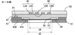
図3は、図1のサスペンション基板1のうち一点鎖線で取り囲まれる部分Qの拡大平面図である。図4は、図3のA−A線断面図である。図5は、図3のB−B線断面図である。図6は、図3のC−C線断面図である。図3に示すように、図1の部分Qでは、書込用配線パターンW1,W2の線路LA4,LA5,LB3,LB4および電源用配線パターンP1が前後方向に直交する方向に並ぶように形成されている。
FIG. 3 is an enlarged plan view of a portion Q of the
図4に示すように、支持基板10上に、例えばポリイミドからなる第1の絶縁層41が形成されている。第1の絶縁層41は、薄肉部41Aおよび厚肉部41Bを有する。厚肉部41Bの厚みは、薄肉部41Aの厚みよりも大きい。
As shown in FIG. 4, a first insulating
第1の絶縁層41の薄肉部41A上に、支持基板10よりも高い電気伝導率を有する接地層50が形成されている。接地層50の材料としては、例えば銅が用いられる。支持基板10がステンレス鋼からなる場合には、金または銀を接地層50の材料として用いてもよい。あるいは、金、銀および銅のいずれかを含みかつステンレス鋼よりも高い電気伝導率を有する合金を接地層50の材料として用いてもよい。
A
なお、接地層50は、多層構造を有してもよい。例えば、接地層50は、支持基板10がステンレス鋼からなる場合に、銅層上にニッケル層または銀層が積層された2層構造を有してもよいし、銅層上にニッケル層および金層が積層された3層構造を有してもよい。接地層50が銅層を含む多層構造を有する場合には、銅層の表面を被覆するように、銅層の上面上および側面上にニッケル層、銀層または金層等の他の金属層が形成されてもよい。
The
接地層50の下方における第1の絶縁層41の薄肉部41Aの部分に貫通孔H13が形成される。接地層50は、貫通孔H13内において支持基板10に接触する。貫通孔H13内の接地層50の部分によりビアV3が形成される。これにより、接地層50がビアV3を介して支持基板10に電気的に接続される。
A through hole H13 is formed in the
第1の絶縁層41の厚肉部41B上に、本発明の下部配線パターンとして電源用配線パターンP1が形成されている。電源用配線パターンP1の材料としては、例えば銅が用いられる。なお、電源用配線パターンP1の表面は、ニッケル層または銀層等で被覆されてもよい。
A power supply wiring pattern P1 is formed as a lower wiring pattern of the present invention on the
接地層50および電源用配線パターンP1を覆うように、第1の絶縁層41上に、例えばポリイミドからなる第2の絶縁層42が形成されている。本例では、第2の絶縁層42はさらに接地層50に接触するように形成されている。
A second insulating
第2の絶縁層42上に、本発明の上部配線パターンとして書込用配線パターンW1,W2の線路LA4,LA5,LB3,LB4が形成されている。書込用配線パターンW1,W2の線路LA4,LA5,LB3,LB4の少なくとも一部は、接地層50に重なる。書込用配線パターンW1,W2の材料としては、例えば銅が用いられる。書込用配線パターンW1,W2を覆うように、第2の絶縁層42上に、例えばポリイミドからなる第3の絶縁層60が形成されている。なお、書込用配線パターンW1,W2の表面は、ニッケル層または銀層等で被覆されてもよい。
Lines LA4, LA5, LB3, and LB4 of the writing wiring patterns W1 and W2 are formed on the second insulating
上記の構成により、支持基板10、第1の絶縁層41および第2の絶縁層42の積層方向(以下、基板積層方向と呼ぶ。)において、接地層50と書込用配線パターンW1との間隔d1は、電源用配線パターンP1と書込用配線パターンW1との間隔d2よりも大きくなるように設定される。
With the above configuration, the distance between the
図3では、図4の第1の絶縁層41、第2の絶縁層42および第3の絶縁層60の図示を省略している。また、図3では、書込用配線パターンW1,W2を太い実線およびハッチングで示し、電源用配線パターンP1を太い一点鎖線およびハッチングで示し、接地層50を実線およびドットパターンで示す。さらに、支持基板10を二点鎖線で示す。
In FIG. 3, the first insulating
高い周波数帯域を有する電気信号が書込用配線パターンW1,W2を伝送する場合、書込用配線パターンW1,W2から電磁波が発生する。発生する電磁波が支持基板10または接地層50に入射すると、支持基板10に渦電流が発生し、書込用配線パターンW1,W2と支持基板10または接地層50とが電磁的に結合する。書込用配線パターンW1,W2を伝送する電気信号には、支持基板10または接地層50に発生する渦電流の大きさに応じた損失が生じる。電気信号の損失は、発生する渦電流が大きいほど大きく、発生する渦電流が小さいほど小さい。
When an electric signal having a high frequency band transmits the writing wiring patterns W1 and W2, electromagnetic waves are generated from the writing wiring patterns W1 and W2. When the generated electromagnetic wave is incident on the
ある導体に電磁波が与えられることによりその導体に発生する渦電流は、その導体の電気伝導率が低いほど大きく、その導体の電気伝導率が高いほど小さい。接地層50は、支持基板10に比べて高い電気伝導率を有する。そのため、電磁波により接地層50に発生する渦電流は、電磁波により支持基板10に発生する渦電流よりも小さい。
The eddy current generated in a conductor when an electromagnetic wave is applied to the conductor is larger as the electric conductivity of the conductor is lower, and smaller as the electric conductivity of the conductor is higher. The
上記の構成によれば、書込用配線パターンW1,W2の少なくとも一部と支持基板10との間に接地層50が位置するので、書込用配線パターンW1,W2から支持基板10に向かって放射される電磁波の少なくとも一部は、接地層50に入射し、支持基板10に到達しない。また、接地層50に発生する渦電流は、接地層50と書込用配線パターンW1,W2との間隔が大きいほど小さい。上記の構成によれば、基板積層方向における接地層50と書込用配線パターンW1,W2との間隔d1(図4)が、電源用配線パターンP1と書込用配線パターンW1との間隔d2(図4)よりも大きい。したがって、接地層50が第1の絶縁層41の厚肉部41B上に形成される場合に比べて接地層50に発生する渦電流が小さくされる。これらの結果、高い周波数帯域において書込用配線パターンW1,W2を伝送する電気信号の損失が低減される。
According to the above configuration, since the
書込用配線パターンW1,W2の特性インピーダンスの値は、書込用配線パターンW1,W2と支持基板10および接地層50とが重なる部分の面積に応じて定まる。例えば、書込用配線パターンW1の特性インピーダンスの値は、書込用配線パターンW1の一部と支持基板10および接地層50とが重なる場合に比べて、書込用配線パターンW1全体と支持基板10および接地層50とが重なる場合の方が小さくなる。また、その特性インピーダンスの値は、書込用配線パターンW1と支持基板10および接地層50とが重ならない場合に比べて、書込用配線パターンW1の一部と支持基板10および接地層50とが重なる場合の方が小さくなる。
The value of the characteristic impedance of the writing wiring patterns W1 and W2 is determined according to the area of the portion where the writing wiring patterns W1 and W2 overlap with the
そこで、本実施の形態では、各書込用配線パターンW1,W2の特性インピーダンスの値が所望の値に近づくように、書込用配線パターンW1,W2と支持基板10および接地層50とが重なる部分の面積が調整される。具体的には、図3、図5および図6に示すように、予め設定されるインピーダンスに応じて、書込用配線パターンW1,W2に重なる複数の第1の開口部19が支持基板10に形成される。また、複数の第1の開口部19にそれぞれ重なる複数の第2の開口部59が接地層50に形成される。
Therefore, in the present embodiment, the writing wiring patterns W1 and W2 overlap with the
複数の第1の開口部19および複数の第2の開口部59は、基本的に書込用配線パターンW1,W2が延びる方向に並ぶように間欠的に形成される。それにより、書込用配線パターンW1,W2の特性インピーダンスの均一性を向上させることができる。
The plurality of
なお、設定されるインピーダンスによっては、複数の第1の開口部19および複数の第2の開口部59は、支持基板10および接地層50にそれぞれ形成されなくてもよい。または、設定されるインピーダンスによっては、支持基板10および接地層50には、1つの第1の開口部19および1つの第2の開口部59のみが形成されてもよい。
Depending on the impedance to be set, the plurality of
図3に示すように、互いに重なり合う第1の開口部19および第2の開口部59は、サスペンション基板1を基板積層方向に沿って見た場合に第1の開口部19の内縁が第2の開口部59の内縁を取り囲むように形成される。この場合、図5に示すように、書込用配線パターンW1,W2に直交する方向においては、接地層50の各第2の開口部59の寸法d4が対応する支持基板10の第1の開口部19の寸法d3に比べて小さい。また、図6に示すように、書込用配線パターンW1,W2に平行な方向においては、接地層50の各第2の開口部59の寸法d6が対応する支持基板10の第1の開口部19の寸法d5に比べて小さい。
As shown in FIG. 3, the
このような構成により、支持基板10および接地層50に第1の開口部19および第2の開口部59をそれぞれ設けつつ、書込用配線パターンW1,W2から支持基板10に向かって放射される電磁波が支持基板10に到達することを抑制することができる。したがって、各書込用配線パターンW1,W2の特性インピーダンスの値を所望の値に調整しつつ、高い周波数帯域において書込用配線パターンW1,W2を伝送する電気信号の損失を低減することができる。
With such a configuration, the
(3)交差領域
図7は、図2の交差領域CN1の拡大平面図である。図8は、図7のD−D線断面図である。図7では、図4の第1の絶縁層41、第2の絶縁層42および第3の絶縁層60の図示を省略している。また、図7では、書込用配線パターンW1(図2)の線路LA3,LA5および書込用配線パターンW2(図2)の線路LB3を太い実線およびハッチングで示す。また、接地層50を実線およびドットパターンで示す。さらに、支持基板10を二点鎖線で示す。図2の交差領域CN2は、交差領域CN1と同様の構成を有する。
(3) Intersection region FIG. 7 is an enlarged plan view of the intersection region CN1 of FIG. FIG. 8 is a cross-sectional view taken along the line DD of FIG. In FIG. 7, the first insulating
図7および図8に示すように、支持基板10のうち交差領域CN1が形成される部分には、環状開口部18が形成される。これにより、支持基板10の一部に、他の部分から電気的に分離された島状の部分が形成される。以下の説明では、支持基板10のうち島状の部分を配線部10Xと呼び、支持基板10のうち配線部10Xを除く部分を支持部10Yと呼ぶ。配線部10Xおよび支持部10Yは、環状開口部18により電気的に分離されている。
As shown in FIGS. 7 and 8, an
配線部10Xの上方を通って延びるように書込用配線パターンW2の線路LB3が配置され、線路LB3の両側に書込用配線パターンW1の線路LA3の他端部および線路LA5の一端部が配置される。
The line LB3 of the writing wiring pattern W2 is arranged so as to extend above the
線路LA3の他端部および線路LA5の一端部には、円形の接続部G1,G2がそれぞれ設けられる。また、接続部G1の下方における第1の絶縁層41および第2の絶縁層42の部分に貫通孔H11が形成され、接続部G2の下方における第1の絶縁層41および第2の絶縁層42の部分に貫通孔H12が形成される。
Circular connecting portions G1 and G2 are provided at the other end of the line LA3 and one end of the line LA5, respectively. Further, through holes H11 are formed in the portions of the first insulating
接続部G1は、貫通孔H11内において配線部10Xに接触する。接続部G2は、貫通孔H12内において配線部10Xに接触する。貫通孔H11内の接続部G1の部分によりビアV1が形成され、貫通孔H12内の接続部G2の部分によりビアV2が形成される。これにより、線路LA3,LA5が、ビアV1,V2および配線部10Xを介して電気的に接続される。
The connecting portion G1 contacts the
接続部G1,G2の形状は、円形に限らず、楕円形、三角形、四角形または扇形等の他の形状であってもよい。また、貫通孔H11,H12の横断面形状は、楕円形、三角形、四角形または扇形等の他の形状であってもよい。 The shape of the connecting portions G1 and G2 is not limited to a circle, and may be another shape such as an ellipse, a triangle, a quadrangle, or a fan. Further, the cross-sectional shapes of the through holes H11 and H12 may be other shapes such as an ellipse, a triangle, a quadrangle, or a fan.
このように、本実施の形態においては、線路LA3と線路LA5とが交差領域CN1のビアV1,V2および配線部10Xを介して電気的に接続される。また、線路LB3(図2)と線路LB5(図2)とが交差領域CN2(図2)のビアV1,V2および配線部10Xを介して電気的に接続される。
As described above, in the present embodiment, the line LA3 and the line LA5 are electrically connected via the vias V1 and V2 of the intersection region CN1 and the
これにより、書込用配線パターンW1と書込用配線パターンW2とを互いに干渉させることなく、図2の書込用配線パターンW1の線路LA4,LA5と図2の書込用配線パターンW2の線路LB3,LB4とを交互に並ぶように配置することができる。 As a result, the lines LA4 and LA5 of the writing wiring pattern W1 of FIG. 2 and the lines of the writing wiring pattern W2 of FIG. 2 do not interfere with each other without causing the writing wiring pattern W1 and the writing wiring pattern W2 to interfere with each other. LB3 and LB4 can be arranged so as to be arranged alternately.
上記の構成によれば、線路LA4の一側面および他側面ならびに線路LA5の一側面および他側面のうち3つの側面と、線路LB3の一側面および他側面ならびに線路LB4の一側面および他側面のうち3つの側面とが、互いに対向する。それにより、書込用配線パターンW1,W2の間の対向面積が大きくなり、書込用配線パターンW1,W2のキャパシタンスが大きくなる。その結果、書込用配線パターンW1,W2の特性インピーダンスが低減される。 According to the above configuration, one side surface and the other side surface of the line LA4, three side surfaces of the one side surface and the other side surface of the line LA5, one side surface and the other side surface of the line LB3, and one side surface and the other side surface of the line LB4. The three sides face each other. As a result, the facing area between the writing wiring patterns W1 and W2 becomes large, and the capacitance of the writing wiring patterns W1 and W2 becomes large. As a result, the characteristic impedance of the writing wiring patterns W1 and W2 is reduced.
なお、図1の読取用配線パターンR1,R2は、例えばそれぞれ1つの線路により図4の第2の絶縁層42上に形成される。あるいは、読取用配線パターンR1,R2は、上記の書込用配線パターンW1,W2の構成と同様に、電気信号が分岐して伝送するように構成された複数の線路により形成されてもよい。
The reading wiring patterns R1 and R2 of FIG. 1 are formed on the second insulating
(4)サスペンション基板の製造方法
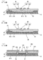
サスペンション基板1の製造方法について説明する。図9〜図15は、図1のサスペンション基板1の製造方法を示す模式的工程断面図である。図9〜図15の各図においては、(a)が図3のA−A線断面図に対応し、(b)が図3のB−B線断面図に対応し、(c)が図7のD−D線断面図に対応する。ここでは、図1のタング部12、複数の接続端子21〜26,31〜36、複数の孔部H、読取用配線パターンR1,R2および電源用配線パターンP2の形成工程についての説明は省略する。
(4) Manufacturing Method of Suspension Board The manufacturing method of the
初めに、図9(a)〜(c)に示すように、例えばステンレス鋼からなる長尺状の支持基板10上に、例えば感光性ポリイミド樹脂前駆体41pを塗布する。支持基板10の厚みは、例えば8μm以上100μm以下である。
First, as shown in FIGS. 9 (a) to 9 (c), for example, a photosensitive
次に、図10(a)〜(c)に示すように、露光機において所定の階調を有するマスクを介して支持基板10上の感光性ポリイミド樹脂前駆体41pに紫外線を照射する。これにより、ポリイミドからなる第1の絶縁層41が形成される。厚肉部41Bの厚みは、例えば1μm以上25μm以下である。薄肉部41Aの厚みは、厚肉部41Bの厚みよりもわずかに小さい。
Next, as shown in FIGS. 10A to 10C, the photosensitive
また、図10(a)に示すように、接地層50が形成されることになる第1の絶縁層41の薄肉部41Aの部分に貫通孔H13が形成される。それにより、支持基板10の部分が貫通孔H13を通して第1の絶縁層41よりも上方の空間に露出する。さらに、図10(c)に示すように、図2の交差領域CN1を構成することになる第1の絶縁層41の厚肉部41Bの部分に間隔を隔てて並ぶ2つの貫通孔H1,H2が形成される。それにより、支持基板10の上面の2つの部分が2つの貫通孔H1,H2を通して第1の絶縁層41よりも上方の空間に露出する。
Further, as shown in FIG. 10A, a through hole H13 is formed in the
次に、図11(a)〜(c)に示すように、第1の絶縁層41の薄肉部41A上に銅からなる接地層50を形成する。また、接地層50の形成と同時に、第1の絶縁層41の厚肉部41B上に銅からなる電源用配線パターンP1を形成する。このとき、図11(b)に示すように、接地層50には、図3の複数の第2の開口部59が形成される。接地層50および電源用配線パターンP1の厚みは、例えば1μm以上20μm以下である。さらに、図11(a)に示すように、接地層50の形成時には、貫通孔H13の内部に銅が充填される。それにより、ビアV3が形成される。
Next, as shown in FIGS. 11A to 11C, a
次に、図12(a)〜(c)に示すように、接地層50および電源用配線パターンP1を覆うように、第1の絶縁層41上にポリイミドからなる第2の絶縁層42を形成する。このとき、第2の絶縁層42は、接地層50に接触するように形成される。第2の絶縁層42の厚みは、例えば1μm以上25μm以下である。
Next, as shown in FIGS. 12A to 12C, a second insulating
また、図12(c)に示すように、第1の絶縁層41の2つの貫通孔H1,H2にそれぞれ重なるように第2の絶縁層42の部分に貫通孔H3,H4が形成される。貫通孔H1と貫通孔H3とが連なることにより貫通孔H11となり、貫通孔H2と貫通孔H4とが連なることにより貫通孔H12となる。
Further, as shown in FIG. 12C, through holes H3 and H4 are formed in the portion of the second insulating
次に、図13(a)〜(c)に示すように、少なくとも一部が接地層50に重なるように第2の絶縁層42上に銅からなる書込用配線パターンW1,W2を形成する。本例では、図13(a)に示すように、書込用配線パターンW1,W2の線路LA4,LA5,LB3,LB4の一部が接地層50上に位置する。また、図13(b)に示すように、線路LA4,LA5,LB3,LB4の他の部分が接地層50に形成される複数の第2の開口部59上に位置する。さらに、図13(c)に示すように、書込用配線パターンW1の線路LA3の他端部に接続部G1が位置し、書込用配線パターンW1の線路LA5の一端部に接続部G2が位置する。線路LA3,LA5の形成時には、2つの貫通孔H11,H12の内部に銅が充填される。それにより、ビアV1,V2が形成される。
Next, as shown in FIGS. 13 (a) to 13 (c), writing wiring patterns W1 and W2 made of copper are formed on the second insulating
書込用配線パターンW1,W2の厚みは、例えば1μm以上20μm以下である。書込用配線パターンW1,W2を構成する各線路LA1〜LA5,LB1〜LB5の幅は、例えば6μm以上100μm以下である。また、線路LA4,LB3,LA5,LB4のうち隣り合う各2つの線路の間隔は、例えば6μm以上100μm以下である。各ビアV1,V2の外径は、例えば15μm以上150μm以下である。 The thickness of the writing wiring patterns W1 and W2 is, for example, 1 μm or more and 20 μm or less. The width of each of the lines LA1 to LA5 and LB1 to LB5 constituting the writing wiring patterns W1 and W2 is, for example, 6 μm or more and 100 μm or less. Further, the distance between two adjacent lines of the lines LA4, LB3, LA5, and LB4 is, for example, 6 μm or more and 100 μm or less. The outer diameter of each via V1 and V2 is, for example, 15 μm or more and 150 μm or less.
次に、図14(a)〜(c)に示すように、書込用配線パターンW1,W2を覆うように、第2の絶縁層42上にポリイミドからなる第3の絶縁層60を形成する。第3の絶縁層60は、書込用配線パターンW1,W2を保護するために用いられる。第3の絶縁層60の厚みは、例えば2μm以上25μm以下である。
Next, as shown in FIGS. 14A to 14C, a third insulating
最後に、図15(a)〜(c)に示すように、支持基板10の外縁を設計寸法に応じて加工するとともに、支持基板10に複数の第1の開口部19および環状開口部18を形成する。複数の第1の開口部19は、複数の第2の開口部59をそれぞれ取り囲む。環状開口部18は、ビアV1,V2に接する支持基板10の部分を取り囲む。それにより、サスペンション基板1が完成する。
Finally, as shown in FIGS. 15A to 15C, the outer edge of the
(5)効果
本実施の形態に係るサスペンション基板1においては、支持基板10上に第1の絶縁層41が形成される。第1の絶縁層41の薄肉部41A上に接地層50が形成され、第1の絶縁層41の厚肉部41B上に電源用配線パターンP1が形成される。また、接地層50および電源用配線パターンP1を覆うように第1の絶縁層41上に第2の絶縁層42が形成される。さらに、少なくとも一部が接地層50に重なるように第2の絶縁層42上に書込用配線パターンW1,W2が形成される。この場合、電源用配線パターンP1および書込用配線パターンW1,W2の各々に電気信号を伝送させることができる。
(5) Effect In the
上記の構成によれば、書込用配線パターンW1,W2の少なくとも一部と支持基板10との間に接地層50が位置するので、書込用配線パターンW1,W2から支持基板10に向かって放射される電磁波の少なくとも一部は、接地層50に入射し、支持基板10に到達しない。また、上記の構成によれば、基板積層方向における接地層50と書込用配線パターンW1,W2との間隔d1が、電源用配線パターンP1と書込用配線パターンW1との間隔d2よりも大きく設定される。この場合、接地層50が第1の絶縁層41の厚肉部41B上に形成される場合に比べて接地層50に発生する渦電流が小さくされる。これらの結果、高い周波数帯域において書込用配線パターンW1,W2を伝送する電気信号の損失が低減される。
According to the above configuration, since the
上記の例では、ステンレス鋼からなる支持基板10が用いられる。この場合、支持基板10において、ステンレス鋼により書込用配線パターンW1,W2、読取用配線パターンR1,R2および電源用配線パターンP1,P2を支持するために必要とされる十分な剛性を確保することができる。また、ステンレス鋼の表面には不動態膜が形成される。それにより、腐食による支持基板10の劣化が抑止される。
In the above example, the
[2]第2の実施の形態
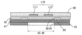
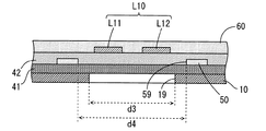
第2の実施の形態に係るサスペンション基板について、第1の実施の形態に係るサスペンション基板1とは異なる点を説明する。図16、図17および図18は、第2の実施の形態に係るサスペンション基板の一部拡大平面図である。図16、図17および図18は、それぞれ図3のA−A線断面図、B−B線断面図およびC−C線断面図に相当する。
[2] Second Embodiment The suspension substrate according to the second embodiment will be described as being different from the
図16および図17に示すように、本実施の形態に係るサスペンション基板1においては、電源用配線パターンP1,P2が第1の絶縁層41上に形成されない。また、図16〜図18に示すように、第1の絶縁層41は、薄肉部41Aと厚肉部41Bとを有さずに、均一な厚みに形成される。
As shown in FIGS. 16 and 17, in the
第1の実施の形態と同様に、各書込用配線パターンW1,W2の特性インピーダンスの値が所望の値に近づくように、書込用配線パターンW1,W2と支持基板10および接地層50とが重なる部分の面積が調整される。具体的には、書込用配線パターンW1,W2に重なる複数の第1の開口部19が支持基板10に形成される。また、複数の第1の開口部19にそれぞれ重なる複数の第2の開口部59が接地層50に形成される。サスペンション基板1を基板積層方向に沿って見た場合に、第1の開口部19の内縁が第2の開口部59の内縁を取り囲む。
Similar to the first embodiment, the writing wiring patterns W1 and W2, the
この場合、図17に示すように、書込用配線パターンW1,W2に直交する方向においては、接地層50の各第2の開口部59の寸法d4が対応する支持基板10の第1の開口部19の寸法d3に比べて小さい。また、図18に示すように、書込用配線パターンW1,W2に平行な方向においては、接地層50の各第2の開口部59の寸法d6が対応する支持基板10の第1の開口部19の寸法d5に比べて小さい。
In this case, as shown in FIG. 17, in the direction orthogonal to the writing wiring patterns W1 and W2, the first opening of the
上記の構成によれば、書込用配線パターンW1,W2の少なくとも一部と支持基板10との間に接地層50が位置するので、書込用配線パターンW1,W2から支持基板10に向かって放射される電磁波の少なくとも一部は、接地層50に入射し、支持基板10に到達しない。また、第1の開口部19および第2の開口部59の大きさおよび数を調整することにより、書込用配線パターンW1,W2の特性インピーダンスの値を容易に調整することができる。
According to the above configuration, since the
ここで、接地層50の第2の開口部59の寸法は、書込用配線パターンW1,W2と支持基板10との間に接地層50の一部が存在するように設定される。そのため、支持基板10および接地層50に第1の開口部19および第2の開口部59をそれぞれ設けつつ、書込用配線パターンW1,W2から支持基板10に向かって放射される電磁波が支持基板10に到達することを抑制することができる。これにより、書込用配線パターンW1,W2の特性インピーダンスの値を所望の値に調整しつつ、高い周波数帯域において書込用配線パターンW1,W2を伝送する電気信号の損失を低減することができる。
Here, the dimensions of the
なお、本実施の形態に係るサスペンション基板1の製造方法は、以下の点を除き、第1の実施の形態に係るサスペンション基板1の製造方法と同様である。図10(a)〜(c)の工程において、階調を有さないマスクを介して支持基板10上の感光性ポリイミド樹脂前駆体41pに紫外線が照射される。また、図11(a)〜(c)の工程において、電源用配線パターンP1,P2が第1の絶縁層41上に形成されない。
The method for manufacturing the
[3]他の実施の形態
(1)上記実施の形態においては、支持基板10の配線部10Xを通して線路LA3と線路LA5とが電気的に接続されるが、本発明はこれに限定されない。図19は、他の実施の形態に係るサスペンション基板のうち図7のD−D線に対応する部分の断面図である。
[3] Other Embodiments (1) In the above embodiment, the line LA3 and the line LA5 are electrically connected through the
図19に示すように、本実施の形態に係るサスペンション基板1は、接続部G1,G2に重なるように第1の絶縁層41の厚肉部41B上に配置された中継パターン51をさらに備える。中継パターン51は、図1の書込用配線パターンW1,W2等と同一の材料により書込用配線パターンW1,W2と同時に形成することができる。
As shown in FIG. 19, the
接続部G1,G2の下方における第2の絶縁層42の部分に貫通孔H11,H12がそれぞれ形成される。接続部G1は貫通孔H11内において中継パターン51に接触し、接続部G2は貫通孔H12内において中継パターン51に接触する。貫通孔H11内の接続部G1の部分によりビアV1が形成され、貫通孔H12内の接続部G2の部分によりビアV2が形成される。これにより、線路LA3,LA5が、ビアV1,V2、中継パターン51を介して電気的に接続される。
Through holes H11 and H12 are formed in the portion of the second insulating
図19の構成においては、支持基板10の一部を配線部10Xとして用いる必要がない。そのため、支持基板10に図8の環状開口部18が形成されない。
In the configuration of FIG. 19, it is not necessary to use a part of the
(2)上記実施の形態においては、接地層50がビアV3を介して支持基板10に電気的に接続されるが、本発明はこれに限定されない。接地層50がビアV3を介さずに支持基板10に電気的に接続されてもよい。
(2) In the above embodiment, the
(3)第1の実施の形態においては、電源用配線パターンP1,P2は低い周波数帯域を有する電気信号を伝送させるための低周波線路であるが、本発明はこれに限定されない。電源用配線パターンP1,P2を伝送する電気信号の損失がある程度許容される場合には、電源用配線パターンP1,P2に高い周波数帯域を有する電気信号を伝送させてもよい。すなわち、電源用配線パターンP1,P2を高周波線路として用いてもよい。 (3) In the first embodiment, the power supply wiring patterns P1 and P2 are low-frequency lines for transmitting an electric signal having a low frequency band, but the present invention is not limited thereto. If the loss of the electric signal for transmitting the power supply wiring patterns P1 and P2 is tolerated to some extent, the electric signal having a high frequency band may be transmitted to the power supply wiring patterns P1 and P2. That is, the power supply wiring patterns P1 and P2 may be used as the high frequency line.
(4)第1の実施の形態においては、支持基板10の第1の開口部19の内縁が接地層50の第2の開口部59の内縁を取り囲むが、本発明はこれに限定されない。支持基板10の第1の開口部19の内縁が接地層50の第2の開口部59の内縁と重なっていてもよい。あるいは、接地層50の第2の開口部59の内縁が支持基板10の第1の開口部19の内縁を取り囲んでもよい。
(4) In the first embodiment, the inner edge of the
(5)第1の実施の形態においては、第1の絶縁層41が薄肉部41Aと厚肉部41Bと有するが、本発明はこれに限定されない。第1の絶縁層41が薄肉部41Aと厚肉部41Bと有さずに、均一な厚みに形成されてもよい。この場合、接地層50の厚みは、電源用配線パターンP1の厚みよりも小さく形成される。
(5) In the first embodiment, the first insulating
[4]請求項の各構成要素と実施の形態の各部との対応関係
以下、請求項の各構成要素と実施の形態の各部との対応の例について説明するが、本発明は下記の例に限定されない。
[4] Correspondence between each component of the claim and each part of the embodiment The example of correspondence between each component of the claim and each part of the embodiment will be described below. Not limited.
上記実施の形態においては、支持基板10が支持基板の例であり、第1の絶縁層41が第1の絶縁層の例であり、第2の絶縁層42が第2の絶縁層の例である。第3の絶縁層60が第3の絶縁層の例であり、接地層50が接地層の例であり、電源用配線パターンP1が下部配線パターンの例であり、書込用配線パターンW1,W2が上部配線パターンの例である。
In the above embodiment, the
サスペンション基板1が配線回路基板の例であり、薄肉部41Aが第1の部分の例であり、厚肉部41Bが第2の部分の例であり、第1の開口部19が第1の開口部の例である。第2の開口部59が第2の開口部の例であり、ビアV1が第1のビアの例であり、ビアV2が第2のビアの例であり、ビアV3が第3のビアの例であり、支持部10Yが支持部の例である。
The
配線部10Xが配線部の例であり、書込用配線パターンW1が第1の信号線路の例であり、書込用配線パターンW2が第2の信号線路の例であり、線路LA4が第1の分岐線路の例である。線路LA5が第2の分岐線路の例であり、線路LB3が第3の分岐線路の例であり、線路LB4が第4の分岐線路の例であり、中継パターン51が中継パターンの例である。
The
請求項の各構成要素として、請求項に記載されている構成または機能を有する他の種々の要素を用いることもできる。 As each component of the claim, various other components having the structure or function described in the claim can also be used.
[5]実施例
(1)第1の実施の形態についての実施例および比較例
第1の実施の形態についての実施例1,2および比較例1,2として、以下のサスペンション基板を想定する。図20(a)は実施例1に係るサスペンション基板の平面図であり、図20(b)は図20(a)のJ1−J1線断面図である。
[5] Examples (1) Examples and Comparative Examples of the First Embodiment As Examples 1 and 2 and Comparative Examples 1 and 2 of the first embodiment, the following suspension substrates are assumed. 20 (a) is a plan view of the suspension substrate according to the first embodiment, and FIG. 20 (b) is a cross-sectional view taken along the line J1-J1 of FIG. 20 (a).
図20(a)に示すように、実施例1に係るサスペンション基板では、一方向に延びる上部配線パターンL10および下部配線パターンL20が、一方向に直交する他方向に並ぶように形成されている。上部配線パターンL10は、2つの線路L11,L12を含む。線路L11,L12により差動信号線路対が構成される。 As shown in FIG. 20A, in the suspension substrate according to the first embodiment, the upper wiring pattern L10 and the lower wiring pattern L20 extending in one direction are formed so as to be arranged in other directions orthogonal to one direction. The upper wiring pattern L10 includes two lines L11 and L12. Lines L11 and L12 form a differential signal line pair.
図20(b)に示すように、ステンレス鋼からなる支持基板10上にポリイミドからなる第1の絶縁層41が形成される。第1の絶縁層41の薄肉部41A上に銅からなる接地層50が形成される。第1の絶縁層41の厚肉部41B上に銅からなる下部配線パターンL20が形成される。接地層50および下部配線パターンL20を覆うように、第1の絶縁層41上に、ポリイミドからなる第2の絶縁層42が形成される。第2の絶縁層42上に、銅からなる上部配線パターンL10が形成される。上部配線パターンL10を覆うように、第2の絶縁層42上に、ポリイミドからなる第3の絶縁層60が形成される。
As shown in FIG. 20B, a first insulating
図20(a)では、図20(b)の第1の絶縁層41、第2の絶縁層42および第3の絶縁層60の図示を省略している。また、図20(a)では、上部配線パターンL10を太い実線およびハッチングで示し、下部配線パターンL20を太い一点鎖線およびハッチングで示し、接地層50を実線およびドットパターンで示す。さらに、支持基板10を二点鎖線で示す。
In FIG. 20A, the first insulating
実施例1に係るサスペンション基板においては、線路L11,L12および下部配線パターンL20の各々の長さは20mmである。線路L11,L12および下部配線パターンL20の各々の幅d11および厚みd12はそれぞれ80μmおよび8μmである。線路L11,L12の間隔d13は20μmである。接地層50の幅d14は300μmである。下部配線パターンL20および接地層50の各々の厚みd15は4μmである。
In the suspension substrate according to the first embodiment, the lengths of the lines L11 and L12 and the lower wiring pattern L20 are 20 mm, respectively. The width d11 and thickness d12 of the lines L11 and L12 and the lower wiring pattern L20 are 80 μm and 8 μm, respectively. The distance d13 between the lines L11 and L12 is 20 μm. The width d14 of the
第1の絶縁層41の薄肉部41Aの厚みd20および厚肉部41Bの厚みd21は、それぞれ2μmおよび8μmである。第2の絶縁層42の厚みd22および第3の絶縁層60の厚みd23は、それぞれ8μmおよび12μmである。基板積層方向において、接地層50と線路L11,L12との間隔d1は10μmであり、下部配線パターンL20と線路L11,L12との間隔d2は4μmである。なお、実施例1に係るサスペンション基板においては、後述する開口率は0%に設定される。
The thickness d20 of the
図21は実施例2に係るサスペンション基板の平面図である。図22(a)は図21のJ2−J2線断面図であり、図22(b)は図21のJ3−J3線断面図である。図21では、図20(a)の例と同様に、サスペンション基板の複数の構成要素のうち一部の構成要素を互いに異なる態様で示すとともに、他の構成要素の図示を省略している。実施例2に係るサスペンション基板は、以下の点を除いて実施例1に係るサスペンション基板と同じ構成を有する。 FIG. 21 is a plan view of the suspension substrate according to the second embodiment. 22 (a) is a sectional view taken along line J2-J2 of FIG. 21, and FIG. 22 (b) is a sectional view taken along line J3-J3 of FIG. 21. In FIG. 21, as in the example of FIG. 20A, some of the plurality of components of the suspension substrate are shown in different modes from each other, and the other components are not shown. The suspension substrate according to the second embodiment has the same configuration as the suspension substrate according to the first embodiment except for the following points.
図21および図22(a),(b)に示すように、実施例2に係るサスペンション基板においては、上部配線パターンL10に重なる支持基板10の部分に、一方向に並ぶように間欠的に複数の第1の開口部19が形成される。また、接地層50に複数の第1の開口部19に重なる複数の第2の開口部59がそれぞれ形成される。
As shown in FIGS. 21 and 22 (a) and 22 (b), in the suspension substrate according to the second embodiment, a plurality of suspension substrates are intermittently arranged so as to be arranged in one direction on the portion of the
ここで、複数の第1の開口部19と上部配線パターンL10とが重なる部分の面積の合計を開口面積とした場合に、第2の絶縁層42上で上部配線パターンL10が形成される部分の面積(第2の絶縁層42と上部配線パターンL10との接触部の面積)に対する開口面積の割合を開口率と呼ぶ。実施例2に係るサスペンション基板においては、開口率は50%に設定される。
Here, when the total area of the portions where the plurality of
図23(a)は比較例1に係るサスペンション基板の平面図であり、図23(b)は図23(a)のJ4−J4線断面図である。図23(a)では、図20(a)の例と同様に、サスペンション基板の複数の構成要素のうち一部の構成要素を互いに異なる態様で示すとともに、他の構成要素の図示を省略している。比較例1に係るサスペンション基板は、以下の点を除いて実施例1に係るサスペンション基板と同じ構成を有する。 FIG. 23 (a) is a plan view of the suspension substrate according to Comparative Example 1, and FIG. 23 (b) is a sectional view taken along line J4-J4 of FIG. 23 (a). In FIG. 23A, as in the example of FIG. 20A, some of the plurality of components of the suspension board are shown in different modes from each other, and the other components are omitted from the illustration. There is. The suspension substrate according to Comparative Example 1 has the same configuration as the suspension substrate according to Example 1 except for the following points.
図23(a),(b)に示すように、比較例1に係るサスペンション基板においては、第1の絶縁層41が、薄肉部41Aと厚肉部41Bとを有さずに、均一な厚みに形成される。第1の絶縁層41の厚みd21は8μmである。また、接地層50の厚みd15は、下部配線パターンL20の厚みと等しく、4μmである。そのため、基板積層方向における接地層50と線路L11,L12との間隔d1は、基板積層方向における下部配線パターンL20と線路L11,L12との間隔d2と等しく、4μmである。なお、比較例1に係るサスペンション基板においては、開口率は0%に設定される。
As shown in FIGS. 23 (a) and 23 (b), in the suspension substrate according to Comparative Example 1, the first insulating
図24(a)は比較例2に係るサスペンション基板の平面図であり、図24(b)は図24(a)のJ5−J5線断面図であり、図24(c)は図24(a)のJ6−J6線断面図である。図24(a)では、図20(a)の例と同様に、サスペンション基板の複数の構成要素のうち一部の構成要素を互いに異なる態様で示すとともに、他の構成要素の図示を省略している。比較例2に係るサスペンション基板は、以下の点を除いて比較例1に係るサスペンション基板と同じ構成を有する。 24 (a) is a plan view of the suspension substrate according to Comparative Example 2, FIG. 24 (b) is a sectional view taken along line J5-J5 of FIG. 24 (a), and FIG. 24 (c) is FIG. 24 (a). ) Is a cross-sectional view taken along the line J6-J6. In FIG. 24A, as in the example of FIG. 20A, some of the components of the suspension substrate are shown in different modes from each other, and the other components are omitted from the illustration. There is. The suspension substrate according to Comparative Example 2 has the same configuration as the suspension substrate according to Comparative Example 1 except for the following points.
図24(a)〜(c)に示すように、比較例2に係るサスペンション基板においては、実施例2に係るサスペンション基板と同様に、上部配線パターンL10に重なる支持基板10の部分に、一方向に並ぶように間欠的に複数の第1の開口部19が形成される。また、上部配線パターンL10に重なる接地層50の部分に、複数の第1の開口部19にそれぞれ重なるように複数の第2の開口部59が形成される。比較例2に係るサスペンション基板においては、開口率は50%に設定される。
As shown in FIGS. 24A to 24C, in the suspension substrate according to Comparative Example 2, similarly to the suspension substrate according to Example 2, one direction is provided on the portion of the
実施例1,2および比較例1,2に係るサスペンション基板の各部の寸法が下記表1に示される。 The dimensions of each part of the suspension substrate according to Examples 1 and 2 and Comparative Examples 1 and 2 are shown in Table 1 below.

図25は、実施例1,2および比較例1,2に係るサスペンション基板についてのシミュレーション結果を示す図である。図25においては、縦軸はSパラメータSdd21[dB]を表し、横軸は電気信号の周波数[GHz]を表す。また、図25においては、実施例1,2についてのシミュレーション結果をそれぞれ太い実線および太い点線で示す。比較例1,2についてのシミュレーション結果をそれぞれ一点鎖線および二点鎖線で示す。 FIG. 25 is a diagram showing simulation results for suspension substrates according to Examples 1 and 2 and Comparative Examples 1 and 2. In FIG. 25, the vertical axis represents the S parameter Sdd21 [dB], and the horizontal axis represents the frequency [GHz] of the electric signal. Further, in FIG. 25, the simulation results for Examples 1 and 2 are shown by thick solid lines and thick dotted lines, respectively. The simulation results for Comparative Examples 1 and 2 are shown by the alternate long and short dash line and the alternate long and short dash line, respectively.
なお、図25においては、縦軸に示される負の利得は損失を示す。そのため、SパラメータSdd21の値が低いほど減衰量が大きいことを示し、SパラメータSdd21の値が0に近いほど減衰量が小さいことを示す。 In FIG. 25, the negative gain shown on the vertical axis indicates the loss. Therefore, the lower the value of the S parameter Sdd21, the larger the attenuation amount, and the closer the value of the S parameter Sdd21 is to 0, the smaller the attenuation amount.
図25のシミュレーション結果によれば、0〜20GHzの周波数帯域において、実施例1に係るサスペンション基板を伝送する電気信号の減衰量は、比較例1,2に係るサスペンション基板を伝送する電気信号の減衰量よりも小さい。これにより、基板積層方向において、接地層50と線路L11,L12との間隔d1を下部配線パターンL20と線路L11,L12との間隔d2よりも大きくすることにより、広い周波数帯域に渡って電気信号の減衰量を低減することが可能であることがわかった。
According to the simulation result of FIG. 25, in the frequency band of 0 to 20 GHz, the amount of attenuation of the electric signal transmitted through the suspension substrate according to the first embodiment is the attenuation of the electric signal transmitted through the suspension substrate according to Comparative Examples 1 and 2. Less than the amount. As a result, in the substrate stacking direction, the distance d1 between the
また、図25のシミュレーション結果によれば、0〜20GHzの周波数帯域において、実施例2に係るサスペンション基板を伝送する電気信号の減衰量は、実施例1に係るサスペンション基板を伝送する電気信号の減衰量よりもさらに小さい。それにより、開口率を大きく設定することにより、広い周波数帯域に渡って電気信号の減衰量をより低減することが可能であることがわかった。 Further, according to the simulation result of FIG. 25, in the frequency band of 0 to 20 GHz, the amount of attenuation of the electric signal transmitted through the suspension substrate according to the second embodiment is the attenuation of the electric signal transmitted through the suspension substrate according to the first embodiment. Even smaller than the quantity. As a result, it was found that by setting a large aperture ratio, it is possible to further reduce the amount of attenuation of the electric signal over a wide frequency band.
(2)第2の実施の形態についての実施例および比較例
第2の実施の形態についての実施例3および比較例3,4として、以下のサスペンション基板を想定する。図26は、実施例3に係るサスペンション基板の断面図である。図26の断面図は、図17のB−B線断面図に対応する。後述する図27および図28においても同様である。
(2) Examples and Comparative Examples of the Second Embodiment As Examples 3 and Comparative Examples 3 and 4 of the second embodiment, the following suspension substrates are assumed. FIG. 26 is a cross-sectional view of the suspension substrate according to the third embodiment. The cross-sectional view of FIG. 26 corresponds to the cross-sectional view taken along the line BB of FIG. The same applies to FIGS. 27 and 28, which will be described later.
図26に示すように、実施例3に係るサスペンション基板では、ステンレス鋼からなる支持基板10上にポリイミドからなる第1の絶縁層41が形成される。第1の絶縁層41は、均一な厚みを有する。第1の絶縁層41上に銅からなる接地層50が形成される。接地層50を覆うように第1の絶縁層41上にポリイミドからなる第2の絶縁層42が形成される。
As shown in FIG. 26, in the suspension substrate according to the third embodiment, the first insulating
第2の絶縁層42上に、銅からなる上部配線パターンL10が形成される。上部配線パターンL10は、差動信号線路対を構成する2つの線路L11,L12を含む。上部配線パターンL10を覆うように、第2の絶縁層42上に、ポリイミドからなる第3の絶縁層60が形成される。上部配線パターンL10に重なる第1の開口部19が支持基板10に形成される。また、第1の開口部19に重なる第2の開口部59が接地層50に形成される。
An upper wiring pattern L10 made of copper is formed on the second insulating
上部配線パターンL10に直交する方向においては、接地層50の第2の開口部59の寸法d4は、支持基板10の第1の開口部19の寸法d3に比べて小さい。同様に、上部配線パターンL10に平行な方向においては、接地層50の第2の開口部59の寸法d6(図18)は、支持基板10の第1の開口部19の寸法d5(図18)に比べて小さい。
In the direction orthogonal to the upper wiring pattern L10, the dimension d4 of the
図27は、比較例3に係るサスペンション基板の断面図である。比較例3に係るサスペンション基板は、以下の点を除いて実施例3に係るサスペンション基板と同じ構成を有する。図27に示すように、比較例3に係るサスペンション基板では、上部配線パターンL10に直交する方向においては、接地層50の第2の開口部59の寸法d4は、支持基板10の第1の開口部19の寸法d3と等しい。同様に、上部配線パターンL10に平行な方向においては、接地層50の第2の開口部59の寸法d6(図18)は、支持基板10の第1の開口部19の寸法d5(図18)と等しい。
FIG. 27 is a cross-sectional view of the suspension substrate according to Comparative Example 3. The suspension substrate according to Comparative Example 3 has the same configuration as the suspension substrate according to Example 3 except for the following points. As shown in FIG. 27, in the suspension board according to Comparative Example 3, in the direction orthogonal to the upper wiring pattern L10, the dimension d4 of the
図28は、比較例4に係るサスペンション基板の断面図である。比較例4に係るサスペンション基板は、以下の点を除いて実施例3に係るサスペンション基板と同じ構成を有する。図28に示すように、比較例4に係るサスペンション基板では、上部配線パターンL10に直交する方向においては、接地層50の第2の開口部59の寸法d4は、支持基板10の第1の開口部19の寸法d3に比べて大きい。同様に、上部配線パターンL10に平行な方向においては、接地層50の第2の開口部59の寸法d6(図18)は、支持基板10の第1の開口部19の寸法d5(図18)に比べて大きい。
FIG. 28 is a cross-sectional view of the suspension substrate according to Comparative Example 4. The suspension substrate according to Comparative Example 4 has the same configuration as the suspension substrate according to Example 3 except for the following points. As shown in FIG. 28, in the suspension board according to Comparative Example 4, in the direction orthogonal to the upper wiring pattern L10, the dimension d4 of the
実施例3および比較例3,4に係るサスペンション基板の上部配線パターンL10を電気信号が伝送するときの透過特性を表すSパラメータSdd21をシミュレーションにより求めた。図29は、実施例3および比較例3,4に係るサスペンション基板についてのシミュレーション結果を示す図である。図29においては、縦軸はSパラメータSdd21[dB]を表し、横軸は電気信号の周波数[GHz]を表す。また、図29においては、実施例3、比較例3および比較例4についてのシミュレーション結果をそれぞれ実線、一点鎖線および二点鎖線で示す。 The S-parameter Sdd21 representing the transmission characteristic when the electric signal transmits the upper wiring pattern L10 of the suspension substrate according to the third embodiment and the third and fourth comparative examples was obtained by simulation. FIG. 29 is a diagram showing simulation results for the suspension substrates according to Example 3 and Comparative Examples 3 and 4. In FIG. 29, the vertical axis represents the S parameter Sdd21 [dB], and the horizontal axis represents the frequency [GHz] of the electric signal. Further, in FIG. 29, the simulation results for Example 3, Comparative Example 3 and Comparative Example 4 are shown by solid lines, alternate long and short dash lines, and alternate long and short dash lines, respectively.
図29のシミュレーション結果によれば、0〜10GHzの周波数帯域において、実施例3に係るサスペンション基板を伝送する電気信号の減衰量は、比較例3に係るサスペンション基板を伝送する電気信号の減衰量よりも小さい。また、比較例3に係るサスペンション基板を伝送する電気信号の減衰量は、比較例4に係るサスペンション基板を伝送する電気信号の減衰量よりも小さい。これにより、接地層50の第2の開口部59の寸法d4,d6を支持基板10の第1の開口部19の寸法d3,d5に比べてそれぞれ小さくすることにより、広い周波数帯域に渡って電気信号の減衰量を低減することが可能であることがわかった。
According to the simulation result of FIG. 29, the attenuation amount of the electric signal transmitted through the suspension substrate according to the third embodiment is larger than the attenuation amount of the electric signal transmitted through the suspension substrate according to the comparative example 3 in the frequency band of 0 to 10 GHz. Is also small. Further, the amount of attenuation of the electric signal transmitted through the suspension substrate according to Comparative Example 3 is smaller than the amount of attenuation of the electric signal transmitted through the suspension substrate according to Comparative Example 4. As a result, the dimensions d4 and d6 of the
本発明は種々の配線回路基板に有効に利用することができる。 The present invention can be effectively used for various wiring circuit boards.
1 サスペンション基板
10 支持基板
10X 配線部
10Y 支持部
11 開口部
12 タング部
18 環状開口部
19,59 開口部
21〜26 接続端子
31〜36 接続端子
41,42,60 絶縁層
41A 薄肉部
41B 厚肉部
41p 感光性ポリイミド樹脂前駆体
50 接地層
51 中継パターン
90 支持プレート
91 前端領域
92 後端領域
93 中央領域
94 圧電素子実装領域
94h 貫通孔
95,96 圧電素子
CN1,CN2 交差領域
d1,d2,d13 間隔
d3〜d6 寸法
d11,d14 幅
d12,d15,d20〜d23 厚み
G1,G2 接続部
H 孔部
H1〜H4,H11〜H13 貫通孔
L10 上部配線パターン
L11,L12,LA1〜LA5,LB1〜LB5 線路
L20 下部配線パターン
P1,P2 電源用配線パターン
R1,R2 読取用配線パターン
V1〜V3 ビア
W1,W2 書込用配線パターン
1
Claims (13)
前記支持基板上に形成される第1の絶縁層と、
前記支持基板に電気的に接続されるように前記第1の絶縁層上に形成され、前記支持基板よりも高い電気伝導率を有する接地層と、
前記第1の絶縁層上に形成される下部配線パターンと、
前記接地層および前記下部配線パターンを覆うように前記第1の絶縁層上に形成される第2の絶縁層と、
前記接地層に重なるように前記第2の絶縁層上に形成される上部配線パターンとを備え、
前記支持基板、前記第1の絶縁層および前記第2の絶縁層の積層方向において、前記接地層と前記上部配線パターンとの間隔は、前記下部配線パターンと前記上部配線パターンとの間隔よりも大きい、配線回路基板。 A support substrate formed of a conductive material and
A first insulating layer formed on the support substrate and
A ground layer formed on the first insulating layer so as to be electrically connected to the support substrate and having a higher electrical conductivity than the support substrate.
The lower wiring pattern formed on the first insulating layer and
A second insulating layer formed on the first insulating layer so as to cover the ground layer and the lower wiring pattern, and a second insulating layer.
It is provided with an upper wiring pattern formed on the second insulating layer so as to overlap the ground layer.
In the stacking direction of the support substrate, the first insulating layer, and the second insulating layer, the distance between the ground layer and the upper wiring pattern is larger than the distance between the lower wiring pattern and the upper wiring pattern. , Wiring circuit board.
前記接地層は、前記第1の絶縁層の前記第1の部分上に形成され、
前記下部配線パターンは、前記第1の絶縁層の前記第2の部分上に形成される、請求項1記載の配線回路基板。 The first insulating layer includes a first portion having a first thickness and a second portion having a second thickness larger than the first thickness.
The ground layer is formed on the first portion of the first insulating layer.
The wiring circuit board according to claim 1, wherein the lower wiring pattern is formed on the second portion of the first insulating layer.
前記接地層には、前記支持基板の前記第1の開口部に重なる第2の開口部が形成され、
前記上部配線パターンの少なくとも一部は、前記接地層の前記第2の開口部に重なる、請求項1または2記載の配線回路基板。 A first opening is formed in the support substrate.
A second opening that overlaps the first opening of the support substrate is formed in the ground layer.
The wiring circuit board according to claim 1 or 2, wherein at least a part of the upper wiring pattern overlaps with the second opening of the ground layer.
前記支持基板上に形成される第1の絶縁層と、
前記支持基板に電気的に接続されるように前記第1の絶縁層上に形成され、前記支持基板よりも高い電気伝導率を有する接地層と、
前記接地層を覆うように前記第1の絶縁層上に形成される第2の絶縁層と、
前記接地層に重なるように前記第2の絶縁層上に形成される上部配線パターンとを備え、
前記支持基板には、第1の開口部が形成され、
前記接地層には、前記支持基板の前記第1の開口部に重なる第2の開口部が形成され、
前記上部配線パターンの少なくとも一部は、前記接地層の前記第2の開口部に重なり、
前記接地層の前記第2の開口部の寸法は、前記上部配線パターンと前記支持基板との間に前記接地層の一部が存在するように設定される、配線回路基板。 A support substrate formed of a conductive material and
A first insulating layer formed on the support substrate and
A ground layer formed on the first insulating layer so as to be electrically connected to the support substrate and having a higher electrical conductivity than the support substrate.
A second insulating layer formed on the first insulating layer so as to cover the ground layer,
It is provided with an upper wiring pattern formed on the second insulating layer so as to overlap the ground layer.
A first opening is formed in the support substrate.
A second opening that overlaps the first opening of the support substrate is formed in the ground layer.
At least a portion of the top wiring pattern overlaps the second opening of the ground layer.
The dimension of the second opening of the ground layer is set so that a part of the ground layer exists between the upper wiring pattern and the support board.
前記第2の開口部は、前記第1の方向に並ぶように前記接地層に間欠的に複数形成される、請求項3〜5のいずれか一項に記載の配線回路基板。 The upper wiring pattern extends in the first direction.
The wiring circuit board according to any one of claims 3 to 5, wherein a plurality of the second openings are intermittently formed in the ground layer so as to line up in the first direction.
前記支持基板は、前記接地層に電気的に接続された支持部と、前記支持部から電気的に絶縁された配線部とを含み、
前記上部配線パターンは、信号線路対を構成する第1および第2の信号線路を含み、
前記第1の信号線路は、第1および第2の分岐線路を含み、
前記第2の信号線路は、互いに電気的に接続された第3および第4の分岐線路を含み、
前記第1の信号線路の前記第1および第2の分岐線路と前記第2の信号線路の前記第3および第4の分岐線路とは、交互に並ぶように配置され、
前記第1のビアは、前記第1の信号線路の前記第1の分岐線路と前記支持基板の前記配線部とを電気的に接続し、
前記第2のビアは、前記第1の信号線路の前記第2の分岐線路と前記支持基板の前記配線部とを電気的に接続する、請求項1〜6のいずれか一項に記載の配線回路基板。 Further comprising first and second vias penetrating the first and second insulating layers.
The support substrate includes a support portion electrically connected to the ground layer and a wiring portion electrically insulated from the support portion.
The upper wiring pattern includes first and second signal lines constituting a signal line pair.
The first signal line includes first and second branch lines.
The second signal line includes third and fourth branch lines that are electrically connected to each other.
The first and second branch lines of the first signal line and the third and fourth branch lines of the second signal line are arranged so as to be arranged alternately.
The first via electrically connects the first branch line of the first signal line and the wiring portion of the support substrate.
The wiring according to any one of claims 1 to 6, wherein the second via electrically connects the second branch line of the first signal line and the wiring portion of the support substrate. Circuit board.
前記第2の絶縁層を貫通する第1および第2のビアをさらに備え、
前記上部配線パターンは、信号線路対を構成する第1および第2の信号線路を含み、
前記第1の信号線路は、第1および第2の分岐線路を含み、
前記第2の信号線路は、互いに電気的に接続された第3および第4の分岐線路を含み、
前記第1の信号線路の前記第1および第2の分岐線路と前記第2の信号線路の前記第3および第4の分岐線路とは、交互に並ぶように配置され、
前記第1のビアは、前記第1の信号線路の前記第1の分岐線路と前記中継パターンとを電気的に接続し、
前記第2のビアは、前記第1の信号線路の前記第2の分岐線路と前記中継パターンとを電気的に接続する、請求項1〜6のいずれか一項に記載の配線回路基板。 The relay pattern formed on the first insulating layer and
Further provided with first and second vias penetrating the second insulating layer.
The upper wiring pattern includes first and second signal lines constituting a signal line pair.
The first signal line includes first and second branch lines.
The second signal line includes third and fourth branch lines that are electrically connected to each other.
The first and second branch lines of the first signal line and the third and fourth branch lines of the second signal line are arranged so as to be arranged alternately.
The first via electrically connects the first branch line of the first signal line and the relay pattern.
The wiring circuit board according to any one of claims 1 to 6, wherein the second via electrically connects the second branch line of the first signal line and the relay pattern.
前記支持基板に電気的に接続されるように前記第1の絶縁層上に前記支持基板よりも高い電気伝導率を有する接地層を形成し、前記第1の絶縁層上に下部配線パターンを形成するステップと、
前記接地層および前記下部配線パターンを覆うように前記第1の絶縁層上に第2の絶縁層を形成するステップと、
前記接地層に重なるように前記第2の絶縁層上に上部配線パターンを形成するステップとを含み、
前記接地層および前記下部配線パターンを形成するステップは、前記支持基板、前記第1の絶縁層および前記第2の絶縁層の積層方向において、前記接地層と前記上部配線パターンとの間隔が前記下部配線パターンと前記上部配線パターンとの間隔よりも大きくなるように前記接地層および前記下部配線パターンを形成することを含む、配線回路基板の製造方法。 A step of preparing a first insulating layer laminated on a support substrate formed of a conductive material, and
A ground layer having a higher electrical conductivity than the support substrate is formed on the first insulating layer so as to be electrically connected to the support substrate, and a lower wiring pattern is formed on the first insulating layer. Steps to do and
A step of forming a second insulating layer on the first insulating layer so as to cover the ground layer and the lower wiring pattern.
A step of forming an upper wiring pattern on the second insulating layer so as to overlap the ground layer is included.
In the step of forming the ground layer and the lower wiring pattern, the distance between the ground layer and the upper wiring pattern in the stacking direction of the support substrate, the first insulating layer, and the second insulating layer is the lower portion. A method for manufacturing a wiring circuit board, which comprises forming the ground layer and the lower wiring pattern so as to be larger than the distance between the wiring pattern and the upper wiring pattern.
前記支持基板に電気的に接続されるように前記第1の絶縁層上に前記支持基板よりも高い電気伝導率を有する接地層を形成するステップと、
前記接地層を覆うように前記第1の絶縁層上に第2の絶縁層を形成するステップと、
前記接地層に重なるように前記第2の絶縁層上に上部配線パターンを形成するステップと、
前記支持基板に第1の開口部を形成するステップと、
前記接地層に前記支持基板の前記第1の開口部に重なる第2の開口部を形成するステップとを含み、
前記上部配線パターンを形成するステップは、前記上部配線パターンの少なくとも一部が前記接地層の前記第2の開口部に重なるように前記上部配線パターンを形成することを含み、
前記第2の開口部を形成するステップは、前記上部配線パターンと前記支持基板との間に前記接地層の一部が存在するように前記第2の開口部の寸法を設定することを含む、配線回路基板の製造方法。
A step of preparing a first insulating layer laminated on a support substrate formed of a conductive material, and
A step of forming a ground layer having a higher electrical conductivity than the support substrate on the first insulating layer so as to be electrically connected to the support substrate.
A step of forming a second insulating layer on the first insulating layer so as to cover the ground layer,
A step of forming an upper wiring pattern on the second insulating layer so as to overlap the ground layer,
The step of forming the first opening in the support substrate,
The ground layer includes a step of forming a second opening overlapping the first opening of the support substrate.
The step of forming the upper wiring pattern includes forming the upper wiring pattern so that at least a part of the upper wiring pattern overlaps the second opening of the ground layer.
The step of forming the second opening comprises sizing the second opening so that a portion of the grounding layer is present between the upper wiring pattern and the support substrate. Wiring circuit board manufacturing method .
Priority Applications (3)
| Application Number | Priority Date | Filing Date | Title |
|---|---|---|---|
| JP2016173689A JP6909566B2 (en) | 2016-09-06 | 2016-09-06 | Wiring circuit board and its manufacturing method |
| CN201710795624.0A CN107801294B (en) | 2016-09-06 | 2017-09-06 | Wired circuit board and method for manufacturing same |
| US15/696,270 US10327327B2 (en) | 2016-09-06 | 2017-09-06 | Printed circuit board and method of manufacturing the same |
Applications Claiming Priority (1)
| Application Number | Priority Date | Filing Date | Title |
|---|---|---|---|
| JP2016173689A JP6909566B2 (en) | 2016-09-06 | 2016-09-06 | Wiring circuit board and its manufacturing method |
Publications (3)
| Publication Number | Publication Date |
|---|---|
| JP2018041795A JP2018041795A (en) | 2018-03-15 |
| JP2018041795A5 JP2018041795A5 (en) | 2019-09-12 |
| JP6909566B2 true JP6909566B2 (en) | 2021-07-28 |
Family
ID=61281538
Family Applications (1)
| Application Number | Title | Priority Date | Filing Date |
|---|---|---|---|
| JP2016173689A Active JP6909566B2 (en) | 2016-09-06 | 2016-09-06 | Wiring circuit board and its manufacturing method |
Country Status (3)
| Country | Link |
|---|---|
| US (1) | US10327327B2 (en) |
| JP (1) | JP6909566B2 (en) |
| CN (1) | CN107801294B (en) |
Families Citing this family (4)
| Publication number | Priority date | Publication date | Assignee | Title |
|---|---|---|---|---|
| EP3261417A1 (en) * | 2016-06-22 | 2017-12-27 | OSRAM GmbH | A support structure for lighting devices, corresponding lighting device and method |
| WO2020241296A1 (en) * | 2019-05-30 | 2020-12-03 | パナソニックIpマネジメント株式会社 | Structural body, system, and structure |
| US20210392742A1 (en) * | 2020-06-11 | 2021-12-16 | Innogrit Technologies Co., Ltd. | Embedded microstrip with open slot for high speed signal traces |
| KR20220097718A (en) * | 2020-12-31 | 2022-07-08 | 삼성전자주식회사 | Wiring Board and Semiconductor Module Including the Same |
Family Cites Families (19)
| Publication number | Priority date | Publication date | Assignee | Title |
|---|---|---|---|---|
| JP3891912B2 (en) | 2002-10-09 | 2007-03-14 | 日本発条株式会社 | Disk drive suspension |
| JP4222882B2 (en) * | 2003-06-03 | 2009-02-12 | 日東電工株式会社 | Printed circuit board |
| JP4403090B2 (en) | 2005-03-02 | 2010-01-20 | 日東電工株式会社 | Printed circuit board |
| JP4640802B2 (en) * | 2005-07-07 | 2011-03-02 | 日東電工株式会社 | Suspension board with circuit |
| JP4339834B2 (en) * | 2005-08-23 | 2009-10-07 | 日東電工株式会社 | Method for manufacturing suspension board with circuit |
| JP4611159B2 (en) * | 2005-09-20 | 2011-01-12 | 日東電工株式会社 | Printed circuit board |
| JP4330580B2 (en) * | 2005-12-09 | 2009-09-16 | 日本発條株式会社 | Multilayer ground layer head suspension and method for manufacturing the same, multilayer ground layer flexure and method for manufacturing the same |
| JP2008034639A (en) | 2006-07-28 | 2008-02-14 | Nitto Denko Corp | Wired circuit board |
| JP2008282995A (en) | 2007-05-10 | 2008-11-20 | Nitto Denko Corp | Wiring circuit board |
| JP4960918B2 (en) * | 2008-04-02 | 2012-06-27 | 日東電工株式会社 | Printed circuit board |
| US8633395B2 (en) * | 2008-06-06 | 2014-01-21 | National University Corporation Tohoku University | Multilayer wiring board |
| JP5139169B2 (en) | 2008-06-20 | 2013-02-06 | 日東電工株式会社 | Wiring circuit board and manufacturing method thereof |
| JP4547035B2 (en) * | 2008-11-10 | 2010-09-22 | 日東電工株式会社 | Wiring circuit board and manufacturing method thereof |
| CN101908344B (en) * | 2009-06-02 | 2015-03-04 | 日东电工株式会社 | Wiring circuit base plate |
| JP5870496B2 (en) * | 2011-03-18 | 2016-03-01 | 大日本印刷株式会社 | Flexure substrate for suspension, suspension, suspension with head, and hard disk drive |
| JP5861274B2 (en) * | 2011-05-24 | 2016-02-16 | 大日本印刷株式会社 | Flexure substrate for suspension, suspension, suspension with head, and hard disk drive |
| JP2014049170A (en) * | 2012-09-04 | 2014-03-17 | Dainippon Printing Co Ltd | Substrate for suspension, suspension, suspension with element, hard disk drive and manufacturing method for them |
| JP6407511B2 (en) * | 2013-09-05 | 2018-10-17 | 日東電工株式会社 | Wiring circuit board continuity inspection method and wiring circuit board manufacturing method |
| JP6808266B2 (en) * | 2016-05-18 | 2021-01-06 | 日東電工株式会社 | Wiring circuit board and its manufacturing method |
-
2016
- 2016-09-06 JP JP2016173689A patent/JP6909566B2/en active Active
-
2017
- 2017-09-06 US US15/696,270 patent/US10327327B2/en active Active
- 2017-09-06 CN CN201710795624.0A patent/CN107801294B/en active Active
Also Published As
| Publication number | Publication date |
|---|---|
| US20180070438A1 (en) | 2018-03-08 |
| CN107801294B (en) | 2022-04-22 |
| CN107801294A (en) | 2018-03-13 |
| JP2018041795A (en) | 2018-03-15 |
| US10327327B2 (en) | 2019-06-18 |
Similar Documents
| Publication | Publication Date | Title |
|---|---|---|
| JP6909566B2 (en) | Wiring circuit board and its manufacturing method | |
| JP6627648B2 (en) | Circuit board and electronic circuit module using the same | |
| JP5249870B2 (en) | Wiring circuit board and manufacturing method thereof | |
| JP3397707B2 (en) | Substrate with shield plane with various aperture patterns for transmission time and impedance control | |
| CN107306475B (en) | Wired circuit board and method for manufacturing same | |
| US9301386B2 (en) | Printed circuit board and method of manufacturing the same | |
| US9940957B2 (en) | Printed circuit board and method of manufacturing the same | |
| CN110506454B (en) | Connection structure between substrates | |
| JP2011198402A (en) | Flexure substrate for suspension, suspension, suspension with head, and hard disk drive | |
| JP2003008154A (en) | Printed wiring board, coaxial cable, and electronic device | |
| JP5669499B2 (en) | Printed circuit board | |
| US10154579B2 (en) | Printed circuit board and method of manufacturing the same | |
| JP7021329B2 (en) | Wiring circuit board and its manufacturing method | |
| JP6807180B2 (en) | Wiring circuit board and its manufacturing method | |
| JP2010010550A (en) | Mounting structure of electronic part | |
| JP2005347489A (en) | Semiconductor device | |
| JP2006049496A (en) | Printed wiring board | |
| JP2012243857A (en) | Printed board and manufacturing method of printed board | |
| JP5469261B2 (en) | Wiring circuit board and manufacturing method thereof | |
| JP2006114623A (en) | Substrate module, printed circuit board and electronic device employing it | |
| CN117677029A (en) | Signal transmission structure and manufacturing method | |
| JP2021132074A (en) | Coil component and circuit board including the same | |
| KR100954991B1 (en) | Transmission line impedance matching | |
| JP2002368353A (en) | Printed wiring board | |
| JP2009147100A (en) | Multilayer printed wiring board |
Legal Events
| Date | Code | Title | Description |
|---|---|---|---|
| A521 | Request for written amendment filed |
Free format text: JAPANESE INTERMEDIATE CODE: A523 Effective date: 20190731 |
|
| A621 | Written request for application examination |
Free format text: JAPANESE INTERMEDIATE CODE: A621 Effective date: 20190731 |
|
| A977 | Report on retrieval |
Free format text: JAPANESE INTERMEDIATE CODE: A971007 Effective date: 20200427 |
|
| A131 | Notification of reasons for refusal |
Free format text: JAPANESE INTERMEDIATE CODE: A131 Effective date: 20200602 |
|
| A131 | Notification of reasons for refusal |
Free format text: JAPANESE INTERMEDIATE CODE: A131 Effective date: 20201215 |
|
| TRDD | Decision of grant or rejection written | ||
| A01 | Written decision to grant a patent or to grant a registration (utility model) |
Free format text: JAPANESE INTERMEDIATE CODE: A01 Effective date: 20210615 |
|
| A61 | First payment of annual fees (during grant procedure) |
Free format text: JAPANESE INTERMEDIATE CODE: A61 Effective date: 20210705 |
|
| R150 | Certificate of patent or registration of utility model |
Ref document number: 6909566 Country of ref document: JP Free format text: JAPANESE INTERMEDIATE CODE: R150 |