JP6901490B2 - Light emitting element package and lighting equipment including it - Google Patents
Light emitting element package and lighting equipment including it Download PDFInfo
- Publication number
- JP6901490B2 JP6901490B2 JP2018541110A JP2018541110A JP6901490B2 JP 6901490 B2 JP6901490 B2 JP 6901490B2 JP 2018541110 A JP2018541110 A JP 2018541110A JP 2018541110 A JP2018541110 A JP 2018541110A JP 6901490 B2 JP6901490 B2 JP 6901490B2
- Authority
- JP
- Japan
- Prior art keywords
- light emitting
- lead frame
- emitting element
- layer
- fuselage
- Prior art date
- Legal status (The legal status is an assumption and is not a legal conclusion. Google has not performed a legal analysis and makes no representation as to the accuracy of the status listed.)
- Active
Links
Images


Classifications
-
- F—MECHANICAL ENGINEERING; LIGHTING; HEATING; WEAPONS; BLASTING
- F21—LIGHTING
- F21K—NON-ELECTRIC LIGHT SOURCES USING LUMINESCENCE; LIGHT SOURCES USING ELECTROCHEMILUMINESCENCE; LIGHT SOURCES USING CHARGES OF COMBUSTIBLE MATERIAL; LIGHT SOURCES USING SEMICONDUCTOR DEVICES AS LIGHT-GENERATING ELEMENTS; LIGHT SOURCES NOT OTHERWISE PROVIDED FOR
- F21K9/00—Light sources using semiconductor devices as light-generating elements, e.g. using light-emitting diodes [LED] or lasers
- F21K9/90—Methods of manufacture
-
- H—ELECTRICITY
- H01—ELECTRIC ELEMENTS
- H01L—SEMICONDUCTOR DEVICES NOT COVERED BY CLASS H10
- H01L33/00—Semiconductor devices with at least one potential-jump barrier or surface barrier specially adapted for light emission; Processes or apparatus specially adapted for the manufacture or treatment thereof or of parts thereof; Details thereof
- H01L33/48—Semiconductor devices with at least one potential-jump barrier or surface barrier specially adapted for light emission; Processes or apparatus specially adapted for the manufacture or treatment thereof or of parts thereof; Details thereof characterised by the semiconductor body packages
- H01L33/62—Arrangements for conducting electric current to or from the semiconductor body, e.g. lead-frames, wire-bonds or solder balls
-
- F—MECHANICAL ENGINEERING; LIGHTING; HEATING; WEAPONS; BLASTING
- F21—LIGHTING
- F21K—NON-ELECTRIC LIGHT SOURCES USING LUMINESCENCE; LIGHT SOURCES USING ELECTROCHEMILUMINESCENCE; LIGHT SOURCES USING CHARGES OF COMBUSTIBLE MATERIAL; LIGHT SOURCES USING SEMICONDUCTOR DEVICES AS LIGHT-GENERATING ELEMENTS; LIGHT SOURCES NOT OTHERWISE PROVIDED FOR
- F21K9/00—Light sources using semiconductor devices as light-generating elements, e.g. using light-emitting diodes [LED] or lasers
-
- F—MECHANICAL ENGINEERING; LIGHTING; HEATING; WEAPONS; BLASTING
- F21—LIGHTING
- F21S—NON-PORTABLE LIGHTING DEVICES; SYSTEMS THEREOF; VEHICLE LIGHTING DEVICES SPECIALLY ADAPTED FOR VEHICLE EXTERIORS
- F21S2/00—Systems of lighting devices, not provided for in main groups F21S4/00 - F21S10/00 or F21S19/00, e.g. of modular construction
- F21S2/005—Systems of lighting devices, not provided for in main groups F21S4/00 - F21S10/00 or F21S19/00, e.g. of modular construction of modular construction
-
- H—ELECTRICITY
- H01—ELECTRIC ELEMENTS
- H01L—SEMICONDUCTOR DEVICES NOT COVERED BY CLASS H10
- H01L33/00—Semiconductor devices with at least one potential-jump barrier or surface barrier specially adapted for light emission; Processes or apparatus specially adapted for the manufacture or treatment thereof or of parts thereof; Details thereof
- H01L33/36—Semiconductor devices with at least one potential-jump barrier or surface barrier specially adapted for light emission; Processes or apparatus specially adapted for the manufacture or treatment thereof or of parts thereof; Details thereof characterised by the electrodes
- H01L33/40—Materials therefor
- H01L33/405—Reflective materials
-
- H—ELECTRICITY
- H01—ELECTRIC ELEMENTS
- H01L—SEMICONDUCTOR DEVICES NOT COVERED BY CLASS H10
- H01L33/00—Semiconductor devices with at least one potential-jump barrier or surface barrier specially adapted for light emission; Processes or apparatus specially adapted for the manufacture or treatment thereof or of parts thereof; Details thereof
- H01L33/36—Semiconductor devices with at least one potential-jump barrier or surface barrier specially adapted for light emission; Processes or apparatus specially adapted for the manufacture or treatment thereof or of parts thereof; Details thereof characterised by the electrodes
- H01L33/40—Materials therefor
- H01L33/42—Transparent materials
-
- H—ELECTRICITY
- H01—ELECTRIC ELEMENTS
- H01L—SEMICONDUCTOR DEVICES NOT COVERED BY CLASS H10
- H01L33/00—Semiconductor devices with at least one potential-jump barrier or surface barrier specially adapted for light emission; Processes or apparatus specially adapted for the manufacture or treatment thereof or of parts thereof; Details thereof
- H01L33/48—Semiconductor devices with at least one potential-jump barrier or surface barrier specially adapted for light emission; Processes or apparatus specially adapted for the manufacture or treatment thereof or of parts thereof; Details thereof characterised by the semiconductor body packages
- H01L33/52—Encapsulations
- H01L33/56—Materials, e.g. epoxy or silicone resin
-
- H—ELECTRICITY
- H01—ELECTRIC ELEMENTS
- H01L—SEMICONDUCTOR DEVICES NOT COVERED BY CLASS H10
- H01L2224/00—Indexing scheme for arrangements for connecting or disconnecting semiconductor or solid-state bodies and methods related thereto as covered by H01L24/00
- H01L2224/01—Means for bonding being attached to, or being formed on, the surface to be connected, e.g. chip-to-package, die-attach, "first-level" interconnects; Manufacturing methods related thereto
- H01L2224/42—Wire connectors; Manufacturing methods related thereto
- H01L2224/47—Structure, shape, material or disposition of the wire connectors after the connecting process
- H01L2224/48—Structure, shape, material or disposition of the wire connectors after the connecting process of an individual wire connector
- H01L2224/481—Disposition
- H01L2224/48151—Connecting between a semiconductor or solid-state body and an item not being a semiconductor or solid-state body, e.g. chip-to-substrate, chip-to-passive
- H01L2224/48221—Connecting between a semiconductor or solid-state body and an item not being a semiconductor or solid-state body, e.g. chip-to-substrate, chip-to-passive the body and the item being stacked
- H01L2224/48245—Connecting between a semiconductor or solid-state body and an item not being a semiconductor or solid-state body, e.g. chip-to-substrate, chip-to-passive the body and the item being stacked the item being metallic
- H01L2224/48247—Connecting between a semiconductor or solid-state body and an item not being a semiconductor or solid-state body, e.g. chip-to-substrate, chip-to-passive the body and the item being stacked the item being metallic connecting the wire to a bond pad of the item
-
- H—ELECTRICITY
- H01—ELECTRIC ELEMENTS
- H01L—SEMICONDUCTOR DEVICES NOT COVERED BY CLASS H10
- H01L2224/00—Indexing scheme for arrangements for connecting or disconnecting semiconductor or solid-state bodies and methods related thereto as covered by H01L24/00
- H01L2224/01—Means for bonding being attached to, or being formed on, the surface to be connected, e.g. chip-to-package, die-attach, "first-level" interconnects; Manufacturing methods related thereto
- H01L2224/42—Wire connectors; Manufacturing methods related thereto
- H01L2224/47—Structure, shape, material or disposition of the wire connectors after the connecting process
- H01L2224/48—Structure, shape, material or disposition of the wire connectors after the connecting process of an individual wire connector
- H01L2224/484—Connecting portions
- H01L2224/4847—Connecting portions the connecting portion on the bonding area of the semiconductor or solid-state body being a wedge bond
- H01L2224/48471—Connecting portions the connecting portion on the bonding area of the semiconductor or solid-state body being a wedge bond the other connecting portion not on the bonding area being a ball bond, i.e. wedge-to-ball, reverse stitch
-
- H—ELECTRICITY
- H01—ELECTRIC ELEMENTS
- H01L—SEMICONDUCTOR DEVICES NOT COVERED BY CLASS H10
- H01L24/00—Arrangements for connecting or disconnecting semiconductor or solid-state bodies; Methods or apparatus related thereto
- H01L24/01—Means for bonding being attached to, or being formed on, the surface to be connected, e.g. chip-to-package, die-attach, "first-level" interconnects; Manufacturing methods related thereto
- H01L24/42—Wire connectors; Manufacturing methods related thereto
- H01L24/47—Structure, shape, material or disposition of the wire connectors after the connecting process
- H01L24/48—Structure, shape, material or disposition of the wire connectors after the connecting process of an individual wire connector
-
- H—ELECTRICITY
- H01—ELECTRIC ELEMENTS
- H01L—SEMICONDUCTOR DEVICES NOT COVERED BY CLASS H10
- H01L25/00—Assemblies consisting of a plurality of individual semiconductor or other solid state devices ; Multistep manufacturing processes thereof
- H01L25/16—Assemblies consisting of a plurality of individual semiconductor or other solid state devices ; Multistep manufacturing processes thereof the devices being of types provided for in two or more different main groups of groups H01L27/00 - H01L33/00, or in a single subclass of H10K, H10N, e.g. forming hybrid circuits
- H01L25/167—Assemblies consisting of a plurality of individual semiconductor or other solid state devices ; Multistep manufacturing processes thereof the devices being of types provided for in two or more different main groups of groups H01L27/00 - H01L33/00, or in a single subclass of H10K, H10N, e.g. forming hybrid circuits comprising optoelectronic devices, e.g. LED, photodiodes
-
- H—ELECTRICITY
- H01—ELECTRIC ELEMENTS
- H01L—SEMICONDUCTOR DEVICES NOT COVERED BY CLASS H10
- H01L33/00—Semiconductor devices with at least one potential-jump barrier or surface barrier specially adapted for light emission; Processes or apparatus specially adapted for the manufacture or treatment thereof or of parts thereof; Details thereof
- H01L33/48—Semiconductor devices with at least one potential-jump barrier or surface barrier specially adapted for light emission; Processes or apparatus specially adapted for the manufacture or treatment thereof or of parts thereof; Details thereof characterised by the semiconductor body packages
- H01L33/483—Containers
- H01L33/486—Containers adapted for surface mounting
-
- H—ELECTRICITY
- H01—ELECTRIC ELEMENTS
- H01L—SEMICONDUCTOR DEVICES NOT COVERED BY CLASS H10
- H01L33/00—Semiconductor devices with at least one potential-jump barrier or surface barrier specially adapted for light emission; Processes or apparatus specially adapted for the manufacture or treatment thereof or of parts thereof; Details thereof
- H01L33/48—Semiconductor devices with at least one potential-jump barrier or surface barrier specially adapted for light emission; Processes or apparatus specially adapted for the manufacture or treatment thereof or of parts thereof; Details thereof characterised by the semiconductor body packages
- H01L33/58—Optical field-shaping elements
- H01L33/60—Reflective elements
-
- H—ELECTRICITY
- H01—ELECTRIC ELEMENTS
- H01L—SEMICONDUCTOR DEVICES NOT COVERED BY CLASS H10
- H01L33/00—Semiconductor devices with at least one potential-jump barrier or surface barrier specially adapted for light emission; Processes or apparatus specially adapted for the manufacture or treatment thereof or of parts thereof; Details thereof
- H01L33/48—Semiconductor devices with at least one potential-jump barrier or surface barrier specially adapted for light emission; Processes or apparatus specially adapted for the manufacture or treatment thereof or of parts thereof; Details thereof characterised by the semiconductor body packages
- H01L33/64—Heat extraction or cooling elements
Description
実施例は発光素子パッケージ及びこれを含む照明装置に関するものである。 The embodiment relates to a light emitting device package and a lighting device including the same.
発光ダイオード(LED:Light Emitting Diode)は化合物半導体の特性を用いて電気を赤外線又は光に変換させて信号をやり取りするとか、光源として使われる半導体素子の一種である。 A light emitting diode (LED: Light Emitting Diode) is a type of semiconductor element used as a light source, such as converting electricity into infrared rays or light to exchange signals by using the characteristics of a compound semiconductor.
III−V族窒化物半導体(group III−V nitride semiconductor)は物理的及び化学的特性によって発光ダイオード(LED)又はレーザーダイオード(LD:Laser Diode)などの発光素子の核心素材として脚光を浴びている。 Group III-V nitride semiconductors are in the limelight as the core material of light emitting devices such as light emitting diodes (LEDs) or laser diodes (LDs) due to their physical and chemical properties. ..
このような発光ダイオードは白熱灯と蛍光灯などの既存の照明器具に使われる水銀(Hg)のような環境有害物質を含んでいなくて環境に優しい優れた特性を有し、長い寿命と低電力消費の特性などの利点があるので、既存の光源を取り替えている。 Such light emitting diodes do not contain environmentally harmful substances such as mercury (Hg) used in existing lighting fixtures such as incandescent lamps and fluorescent lamps, have excellent environmentally friendly properties, and have a long life and low life. It replaces the existing light source because it has advantages such as power consumption characteristics.
発光ダイオードを含む既存の発光素子パッケージの基板はセラミックなどで具現されるため、クラックを発生させ、高い製造コストを有する問題点がある。また、発光ダイオードを含む既存の発光素子パッケージの外周部は剛性が弱くてクラック(crack)が発生する問題点がある。 Since the substrate of the existing light emitting element package including the light emitting diode is embodied in ceramic or the like, there is a problem that cracks are generated and the manufacturing cost is high. Further, there is a problem that the outer peripheral portion of the existing light emitting element package including the light emitting diode has low rigidity and cracks occur.
一実施例は改善された特性を有する発光素子パッケージ及びこれを含む照明装置を提供する。 One embodiment provides a light emitting device package having improved properties and a lighting device including the same.
他の実施例は優れた剛性を有しながらも光抽出効率は維持することができる発光素子パッケージ及びこれを含む照明装置を提供する。 Another embodiment provides a light emitting device package capable of maintaining light extraction efficiency while having excellent rigidity, and a lighting device including the same.
一実施例による発光素子パッケージは、カーボンブラックを含むブラックエポキシモールディングコンパウンド(EMC)を含む胴体;前記胴体によって互いに電気的に離隔した第1及び第2リードフレーム;前記第1及び第2リードフレームの少なくとも一つ上に配置された発光素子;及び前記発光素子を取り囲むように前記胴体と前記第1及び第2リードフレーム上に配置されたモールディング部材を含むことができる。 The light emitting device package according to one embodiment is a fuselage containing a black epoxy molding compound (EMC) containing carbon black; first and second lead frames electrically separated from each other by the fuselage; the first and second lead frames. A light emitting element arranged at least one above; and a molding member arranged on the body and the first and second lead frames so as to surround the light emitting element can be included.
例えば、前記胴体の上面と前記第1及び第2リードフレームのそれぞれの上面は同一平面上に位置してもよい。 For example, the upper surface of the body and the upper surfaces of the first and second lead frames may be located on the same plane.
例えば、前記胴体の上面と前記第1及び第2リードフレームのそれぞれの上面は平らな形状を有してもよい。 For example, the upper surface of the body and the upper surfaces of the first and second lead frames may have a flat shape.
例えば、前記発光素子から前記第1及び第2リードフレームの下端までの熱抵抗は5℃/Wであってもよい。 For example, the thermal resistance from the light emitting element to the lower ends of the first and second lead frames may be 5 ° C./W.
例えば、前記発光素子は発光構造物を含むことができる。 For example, the light emitting element can include a light emitting structure.
例えば、前記発光構造物は、第1導電型半導体層;前記第1導電型半導体層上に配置された活性層;及び前記活性層上に配置された第2導電型半導体層を含むことができる。ここで、発光素子パッケージは前記第2導電型半導体層を前記第2リードフレームに電気的に連結する第1ワイヤをさらに含み、前記第1導電型半導体層は前記第1リードフレームに電気的に連結されることができる。もしくは、前記発光素子パッケージは、前記第1導電型半導体層を前記第1リードフレームに電気的に連結する第1ワイヤ;及び前記第2導電型半導体層を前記第2リードフレームに電気的に連結する第2ワイヤをさらに含むことができる。 For example, the light emitting structure can include a first conductive semiconductor layer; an active layer arranged on the first conductive semiconductor layer; and a second conductive semiconductor layer arranged on the active layer. .. Here, the light emitting element package further includes a first wire that electrically connects the second conductive semiconductor layer to the second lead frame, and the first conductive semiconductor layer electrically connects to the first lead frame. Can be linked. Alternatively, the light emitting device package has a first wire that electrically connects the first conductive semiconductor layer to the first lead frame; and the second conductive semiconductor layer that is electrically connected to the second lead frame. A second wire to be used can be further included.
もしくは、例えば、前記発光構造物は、第1導電型半導体層;前記第1導電型半導体層の下に配置された活性層;及び前記活性層の下に配置された第2導電型半導体層を含み、前記発光素子は、前記発光構造物上に配置された基板;前記第1導電型半導体層の下に配置された第1電極;及び前記第2導電型半導体層の下に配置された第2電極をさらに含むことができる。この場合、前記発光素子パッケージは、前記第1電極と前記第1リードフレームの間に配置された第1半田部;及び前記第2電極と前記第2リードフレームの間に配置された第2半田部をさらに含むことができる。 Alternatively, for example, the light emitting structure includes a first conductive semiconductor layer; an active layer arranged under the first conductive semiconductor layer; and a second conductive semiconductor layer arranged under the active layer. The light emitting element includes a substrate arranged on the light emitting structure; a first electrode arranged under the first conductive semiconductor layer; and a second electrode arranged under the second conductive semiconductor layer. Two electrodes can be further included. In this case, the light emitting element package is the first solder portion arranged between the first electrode and the first lead frame; and the second solder arranged between the second electrode and the second lead frame. Parts can be further included.
例えば、前記モールディング部材は、前記発光素子の側部を取り囲み、前記第1及び第2リードフレーム上に配置された第1モールディング部材;及び前記発光素子の上部を取り囲み、前記第1モールディング部材上に配置された第2モールディング部材を含むことができる。 For example, the molding member surrounds a side portion of the light emitting element, surrounds a first molding member arranged on the first and second lead frames; and surrounds an upper portion of the light emitting element, and is placed on the first molding member. The arranged second molding member can be included.
例えば、前記第1モールディング部材の厚さは前記発光素子の厚さと同一であってもよい。前記胴体の厚さと前記第1及び第2リードフレームの厚さは互いに同一であってもよい。 For example, the thickness of the first molding member may be the same as the thickness of the light emitting element. The thickness of the body and the thickness of the first and second lead frames may be the same as each other.
例えば、前記第1リードフレームは、第1−1層;及び前記第1−1層上に配置され、前記第1−1層より広い第1−2層を含み、前記第2リードフレームは、第2−1層;及び前記第2−1層上に配置され、前記第2−1層より広い第2−2層を含むことができる。前記胴体は、前記第1−1層が収容される第1−1収容空間;前記第2−1層が収容される第2−1収容空間;前記第1−1収容空間と前記第2−1収容空間を互いに離隔させるように配置された隔壁;前記第1−2層が収容され、前記第1−1収容空間上に配置された第1−2収容空間;及び前記第2−2層が収容され、前記第2−1収容空間上に配置された第2−2収容空間を含むことができる。 For example, the first lead frame is arranged on the 1-1 layer; and the 1-1 layer, and includes a 1-2 layer wider than the 1-1 layer, and the second lead frame is a layer. The 2-1st layer; and the 2nd-2nd layer arranged on the 2-1st layer and wider than the 2-1st layer can be included. The fuselage is a 1-1 accommodation space in which the 1-1 layer is accommodated; a 2-1 accommodation space in which the 2-1 layer is accommodated; the 1-1 accommodation space and the 2-. A partition wall arranged so as to separate 1 accommodation space from each other; a 1-2 accommodation space in which the 1-2 layers are accommodated and arranged on the 1-1 accommodation space; and the 2-2 layer. Can include a 2-2 containment space arranged on the 2-1 containment space.
例えば、前記第1−2層は前記第1−2収容空間の外側に突出した少なくとも一つの第1突出部を含み、前記第2−2層は前記第2−2収容空間の外側に突出した少なくとも一つの第2突出部を含み、前記胴体は前記第1及び第2突出部を収容する複数のブラインドホールを含むことができる。 For example, the first and second layers include at least one first protrusion protruding outside the first and second accommodation spaces, and the second and second layers project outside the second and second accommodation spaces. The fuselage may include a plurality of blind holes accommodating the first and second protrusions, including at least one second protrusion.
例えば、前記第1−1層と前記第1−2層は一体型であってもよく、前記第2−1層と前記第2−2層は一体型であってもよい。 For example, the 1-1 layer and the 1-2 layer may be integrated, and the 2-1 layer and the 2-2 layer may be integrated.
例えば、前記発光素子パッケージは、前記第1及び第2リードフレームと一緒に前記モールディング部材を閉じこめるダムをさらに含むことができる。 For example, the light emitting element package may further include a dam that encloses the molding member together with the first and second lead frames.
例えば、前記発光素子パッケージは、前記第1又は第2リードフレームの他の一つ上に配置されたツェナーダイオード;及び前記ツェナーダイオードと前記第2リードフレームを互いに電気的に連結する第3ワイヤをさらに含むことができる。 For example, the light emitting element package comprises a Zener diode arranged on the other one of the first or second lead frames; and a third wire that electrically connects the Zener diode and the second lead frame to each other. Further can be included.
例えば、前記第1及び第2リードフレームは前記胴体に射出成形方式で結合されることができる。 For example, the first and second lead frames can be coupled to the fuselage by an injection molding method.
他の実施例による発光素子パッケージは、第1及び第2リードフレーム;前記第1及び第2リードフレームを互いに電気的に分離させ、前記第1及び第2リードフレームと一緒にキャビティを定義する内側胴体;前記キャビティ内で前記第1又は第2リードフレームの少なくとも1ヶ所に配置された光源;及び前記内側胴体の外側面を取り囲み、前記内側胴体とは違う素材を有する外側胴体を含むことができる。 The light emitting device package according to another embodiment is an inner side that electrically separates the first and second lead frames from each other and defines a cavity together with the first and second lead frames. A fuselage; a light source located at least one of the first or second lead frames in the cavity; and an outer fuselage that surrounds the outer surface of the inner fuselage and has a material different from that of the inner fuselage can be included. ..
例えば、前記内側胴体と前記外側胴体のそれぞれはEMCを含むことができる。 For example, each of the inner fuselage and the outer fuselage can include EMC.
例えば、前記内側胴体はホワイトEMCを含み、前記外側胴体はブラックEMCを含むことができる。 For example, the inner fuselage can include white EMC and the outer fuselage can include black EMC.
例えば、前記内側胴体は、前記第1及び第2リードフレームを互いに電気的に離隔させる下部;及び前記下部から伸びて前記キャビティの側面を形成する側部を含むことができる。 For example, the inner fuselage may include a lower portion that electrically separates the first and second lead frames from each other; and a side portion that extends from the lower portion to form a side surface of the cavity.
例えば、前記内側胴体は前記外側胴体の上部面を貫通する反射突出部をさらに含むことができる。前記反射突出部は前記外側胴体の上部面を2等分するとか4等分することができる。 For example, the inner fuselage may further include reflective protrusions that penetrate the upper surface of the outer fuselage. The reflective protrusion can divide the upper surface of the outer fuselage into two or four equal parts.
例えば、前記反射突出部は対称の平面形状を有してもよい。 For example, the reflective protrusion may have a symmetrical planar shape.
例えば、前記内側胴体の下部は複数の貫通孔を含み、前記第1リードフレームは、前記複数の貫通孔の一部に挿入されて配置された第1下側リードフレーム;及び前記第1下側リードフレーム上に配置され、前記キャビティの底面の一部を形成する第1上側リードフレームを含み、前記第2リードフレームは、前記複数の貫通孔の残りに挿入されて配置された第2下側リードフレーム;及び前記第2下側リードフレーム上に配置され、前記キャビティの前記底面の残りを形成する第2上側リードフレームを含むことができる。 For example, the lower portion of the inner fuselage includes a plurality of through holes, and the first lead frame is a first lower lead frame inserted and arranged in a part of the plurality of through holes; and the first lower side. A second lower side that is placed on the lead frame and includes a first upper lead frame that forms part of the bottom surface of the cavity, the second lead frame being inserted and placed in the rest of the plurality of through holes. A lead frame; and a second upper lead frame that is placed on the second lower lead frame and forms the rest of the bottom surface of the cavity can be included.
例えば、前記第1下側リードフレームと前記第1上側リードフレームは一体型であってもよく、前記第2下側リードフレームと前記第2上側リードフレームは一体型であってもよい。 For example, the first lower lead frame and the first upper lead frame may be integrated, and the second lower lead frame and the second upper lead frame may be integrated.
例えば、前記第1上側リードフレームと前記第2上側リードフレームと前記内側胴体の下部は前記キャビティの底面に相当する同一平面を形成することができる。 For example, the first upper lead frame, the second upper lead frame, and the lower part of the inner fuselage can form the same plane corresponding to the bottom surface of the cavity.
例えば、前記内側胴体の側部は少なくとも一つの内側締結孔を含み、前記外側胴体は前記内側締結孔と連通する少なくとも一つの外側締結孔を含み、前記第1及び第2リードフレームのそれぞれは前記内側締結孔と前記外側締結孔に埋め込まれて前記内側胴体と前記外側胴体を締結する締結突出部を含むことができる。 For example, the side portion of the inner fuselage includes at least one inner fastening hole, the outer fuselage includes at least one outer fastening hole communicating with the inner fastening hole, and each of the first and second lead frames is said. It may include a fastening protrusion embedded in the inner fastening hole and the outer fastening hole to fasten the inner body and the outer body.
例えば、前記少なくとも一つの内側締結孔は互いに一定の間隔で離隔した複数の内側締結孔を含み、前記少なくとも一つの外側締結孔は互いに一定の間隔で離隔した複数の外側締結孔を含むことができる。 For example, the at least one inner fastening hole may include a plurality of inner fastening holes separated from each other at regular intervals, and the at least one outer fastening hole may include a plurality of outer fastening holes separated from each other at regular intervals. ..
例えば、前記発光素子パッケージは、前記キャビティに埋め込まれて前記光源を取り囲むモールディング部材をさらに含むことができる。 For example, the light emitting device package may further include a molding member embedded in the cavity and surrounding the light source.
例えば、前記発光素子パッケージは、前記キャビティを覆うように配置された上部構造物をさらに含むことができる。 For example, the light emitting device package may further include a superstructure arranged to cover the cavity.
例えば、前記内側胴体と前記外側胴体は対称の平面形状を有してもよい。 For example, the inner body and the outer body may have a symmetrical planar shape.
さらに他の実施例による照明装置は、前記発光素子パッケージを含むことができる。 The lighting device according to still another embodiment can include the light emitting element package.
発光素子パッケージ及びこれを含む照明装置の一実施例はセラミック又はAlNの基板を有する既存の発光素子パッケージより安いコストで製造することができ、優れた剛性、射出性及び工程性を有し、単位時間当たりもっと多い個数で製造することができ、高い設計自由度を有し、優れた放熱特性を有し、クラックと粉塵の発生を防止することができるようにし、他の実施例は内側胴体がブラックEMCより優れた反射性を有するホワイトEMCで具現され、外側胴体がホワイトEMCより優れた強度を有するブラックEMCで具現されるので、優れた光抽出効率を有しながらも強い剛性を有することができる。 An embodiment of a light emitting element package and a lighting device including the same can be manufactured at a lower cost than an existing light emitting element package having a ceramic or AlN substrate, and has excellent rigidity, emission and processability, and is a unit. It can be manufactured in larger quantities per hour, has a high degree of design flexibility, has excellent heat dissipation characteristics, can prevent the generation of cracks and dust, and in other examples the inner fuselage It is embodied in white EMC, which has better reflectivity than black EMC, and the outer body is embodied in black EMC, which has better strength than white EMC, so it can have strong rigidity while having excellent light extraction efficiency. it can.
以下、本発明を具体的に説明するために実施例に基づいて説明し、発明の理解を助けるために添付図面を参照して詳細に説明する。しかし、本発明による実施例は様々な他の形態に変形されることができ、本発明の範囲が以下で詳述する実施例に限定されるものと解釈されてはいけない。本発明の実施例は当該分野で平均的な知識を有する者に本発明をより完全に説明するために提供するものである。 Hereinafter, the present invention will be described in detail based on examples in order to specifically explain the present invention, and will be described in detail with reference to the accompanying drawings in order to assist the understanding of the invention. However, the examples according to the invention can be transformed into various other forms and should not be construed as limiting the scope of the invention to the examples detailed below. The examples of the present invention are provided to those who have average knowledge in the art to more fully explain the present invention.
本発明による実施例の説明において、各要素(element)の“上又は下(on or under)”に形成されるものとして記載される場合、上又は下(on or under)は二つの要素(element)が互いに直接(directly)接触するかあるいは一つ以上の他の要素(element)が前記二つの要素(element)の間に配置されて(indirectly)形成されるものを全て含む。また、“上又は下(on or under)”と表現される場合、一つの要素(element)を基準に上方のみでなく下方の意味も含むことができる。 In the description of the examples according to the present invention, when described as being formed "on or under" of each element, the upper or lower is an element. ) Are in direct contact with each other, or one or more other elements are arranged between the two elements (inventories). Further, when it is expressed as "on or under", it can include not only the upper meaning but also the lower meaning based on one element (element).
また、以下で使われる“第1”及び“第2”、“上/上部/上の”及び“下/下部/下の”などの関係的用語は、そのような実体又は要素間のある物理的又は論理的関係又は手順を必ず要求するか内包しなく、ある一つの実体又は要素を他の実体又は要素と区別するためにのみ用いることもできる。 Also, related terms such as "first" and "second", "upper / upper / upper" and "lower / lower / lower" used below are some physics between such entities or elements. It may be used only to distinguish one entity or element from another, without necessarily requiring or including a physical or logical relationship or procedure.
以下、実施例による発光素子パッケージ1000A、1000B、1000C、1000Dをデカルト座標系を用いて説明するが、実施例はこれに限られない。すなわち、デカルト座標系によると、x軸、y軸及びz軸は互いに直交するが、実施例はこれに限られない。すなわち、x軸、y軸、z軸は直交する代わりに互いに交差してもよい。 Hereinafter, the light emitting element packages 1000A, 1000B, 1000C, and 1000D according to the examples will be described using the Cartesian coordinate system, but the examples are not limited to this. That is, according to the Cartesian coordinate system, the x-axis, y-axis and z-axis are orthogonal to each other, but the embodiment is not limited to this. That is, the x-axis, y-axis, and z-axis may intersect each other instead of being orthogonal to each other.
以下、一実施例及び他の実施例による発光素子パッケージ1000A、1000Bを添付図面に基づいて次のように説明する。 Hereinafter, the light emitting element packages 1000A and 1000B according to one embodiment and another embodiment will be described as follows based on the accompanying drawings.
図1は一実施例による発光素子パッケージ1000Aの全体分解斜視図を示し、図2は図1に示した発光素子パッケージ1000Aの部分結合斜視図を示し、図3は図1及び図2に示した発光素子パッケージ1000Aの中間を切開した断面図を示す。
FIG. 1 shows an overall exploded perspective view of the light emitting
図1〜図3を参照すると、一実施例による発光素子パッケージ1000Aは、胴体110、第1及び第2リードフレーム122、124、発光素子130、モールディング部材140、ツェナーダイオード150、接着層152及び第1及び第3ワイヤ162、164を含む。
Referring to FIGS. 1 to 3, the light emitting
胴体110はカーボンブラック(carbon black)を含むブラックエポキシモールディングコンパウンド(EMC:Epoxy Molding Compound)を含むことができる。胴体110は発光素子パッケージ1000Aのベースに相当する部分である。
The
第1リードフレーム122と第2リードフレーム124は胴体110によって互いに電気的に離隔することができる。第1及び第2リードフレーム122、124は発光素子130に電力を提供する役割をする。また、第1及び第2リードフレーム122、124は発光素子130で発生した光を反射させて光効率を高める役割をすることもでき、発光素子130で発生した熱を外部に排出させる役割をすることもできる。第1及び第2リードフレーム122、124のそれぞれは銅(Cu:Copper)などの電気的伝導性を有する物質で具現されることができるが、実施例は第1及び第2リードフレーム122、124の特定の材質に限られない。
The
第1リードフレーム122は第1−1層122L及び第1−2層122Hを含むことができる。第1−1層122Lは第1リードフレーム122の下層に相当し、第1−2層122Hは第1リードフレーム122の上層に相当する。第1−2層122Hは第1−1層122L上に配置され、第1−1層122Lより広い面積を有することができる。図1及び図2を参照すると、第1−1層122Lと第1−2層122Hは別個の層であるものとして示されているが、実施例はこれに限られない。他の実施例によると、図3に示したように、第1−1層122Lと第1−2層122Hは一体型であってもよい。
The
第2リードフレーム124は第2−1層124L及び第2−2層124Hを含むことができる。第2−1層124Lは第2リードフレーム124の下層に相当し、第2−2層124Hは第2リードフレーム124の上層に相当する。第2−2層124Hは第2−1層124L上に配置され、第2−1層124Lより広い面積を有することができる。図1及び図2を参照すると、第2−1層124Lと第2−2層124Hは別個の層であるものとして示されているが、実施例はこれに限られない。他の実施例によると、図3に示したように、第2−1層124Lと第2−2層124Hは一体型であってもよい。
The
第1リードフレーム122が互いに異なる広さを有する第1−1層及び第1−2層122L、122Hに区分され、第2リードフレーム124が互いに異なる広さを有する第2−1層及び第2−2層124L、124Hに区分されて胴体110に配置される場合、第1及び第2リードフレーム122、124は胴体110に安定的に支持されて固定されることができ、第1及び第2リードフレーム122、124と胴体110間の接触面積が広くなって放熱性がもっと優れることができる。
The
図4は図1〜図3に示した第1及び第2リードフレーム122、124と胴体110の分解斜視図を示し、図5は第1及び第2リードフレーム122、124と胴体110の部分結合斜視図を示し、図6は第1及び第2リードフレーム122、124と胴体110の全体結合斜視図を示す。
FIG. 4 shows an exploded perspective view of the first and second lead frames 122 and 124 and the
図4〜図6を参照すると、胴体110は第1−1及び第2−1収容空間H11、H21、第1−2及び第2−2収容空間H12、H22及び隔壁Bを含むことができる。
With reference to FIGS. 4-6, the
図4を参照すると、第1−1収容空間H11は第1リードフレーム122の第1−1層122Lが収容される空間をなし、第2−1収容空間H21は第2リードフレーム124の第2−1層124Lが収容される空間をなす。ここで、第1−1収容空間H11と第2−1収容空間H21は胴体110の隔壁Bによって互いに離隔して配置されることができる。よって、図5に示したように、第1−1収容空間H11に収容された第1リードフレーム122の第1−1層122Lと第2−1収容空間H21に収容された第2リードフレーム124の第2−1層124Lは胴体110の隔壁Bによって互いに電気的に離隔することができる。
Referring to FIG. 4, the 1-1 accommodation space H11 forms a space in which the 1-1
図5を参照すると、第1−2収容空間H12は第1リードフレーム122の第1−2層122Hが収容される空間をなし、第1−1収容空間H11上に位置する。第2−2収容空間H22は第2リードフレーム124の第2−2層124Hが収容される空間をなし、第2−1収容空間H21上に位置する。ここで、第1−2収容空間H12と第2−2収容空間H22は胴体110の隔壁Bによって互いに離隔して配置されることができる。よって、図6に示したように、第1−2収容空間H12に収容された第1リードフレーム122の第1−2層122Hと第2−2収容空間H22に収容された第2リードフレーム124の第2−2層124Hは隔壁Bによって互いに電気的に離隔することができる。
Referring to FIG. 5, the 1-2 accommodation space H12 forms a space in which the 1-2
また、第1リードフレーム122の第1−2層122Hは第1−2収容空間H12の外側に突出した少なくとも一つの第1突出部P1を含む。第2リードフレーム124の第2−2層124Hは第2−2収容空間H22の外側に突出した少なくとも一つの第2突出部P2を含むことができる。
Further, the first and
胴体110は複数のブラインドホール(blind hole)H31、H32をさらに含むことができる。第1ブラインドホールH31は第1突出部P1を収容し、第2ブラインドホールH32は第2突出部P2を収容することができる形状を有する。
The
第1ブラインドホールH31と第1突出部P1間の結合及び第2ブラインドホールH32と第2突出部P2間の結合によって第1及び第2リードフレーム122、124は胴体110に安定的に支持されて固定されることができ、第1及び第2リードフレーム122、124と胴体110間の接触面積が広くなって放熱性がもっと優れることができる。
The first and second lead frames 122 and 124 are stably supported by the
実施例によると、胴体110がブラックEMCで具現されることにより、図6に示したように、胴体110の上面110Tは平らな(flat)形状を有してもよい。
According to the embodiment, since the
また、第1リードフレーム122の上面122HTと第2リードフレーム124の上面124HTも平らな形状を有してもよい。この場合、胴体110の上面110Tと第1及び第2リードフレーム122、124の上面122HT、124HTは互いに同一平面上に位置することができる。
Further, the upper surface 122HT of the
また、図2を参照すると、胴体110は第1厚さT1を有することができ、第1リードフレーム122と第2リードフレーム124のそれぞれは第2厚さT2を有することができる。図示のように、第1リードフレーム122の第2厚さT2は第1−1層122Lと第1−2層122Hの各厚さを合わせた厚さに相当し、第2リードフレーム124の第2厚さT2は第2−1層124Lと第2−2層124Hの各厚さを合わせた厚さに相当する。
Further, referring to FIG. 2, the
また、図示のように、第1リードフレーム122の第2厚さT2と第2リードフレーム124の第2厚さT2は互いに同一であってもよい。しかし、他の実施例によると、第1リードフレーム122の第2厚さT2と第2リードフレーム124の第2厚さT2は互いに異なってもよい。
Further, as shown in the drawing, the second thickness T2 of the
また、胴体110の第1厚さT1と第1及び第2リードフレーム122、124のそれぞれの第2厚さT2は互いに同一であっても異なってもよい。
Further, the first thickness T1 of the
また、製造工程で後述するように、第1及び第2リードフレーム122、124は胴体110に射出成形(injection molding)方式で結合されることができる。
Further, as will be described later in the manufacturing process, the first and second lead frames 122 and 124 can be coupled to the
また、たとえ図示されてはいないが、第1及び第2リードフレーム122、124の両側面はメッキ処理されることができる。すなわち、第1リードフレーム122において第1−1層122Lの下部面と第1−2層122Hの上部面122HT、及び第2リードフレーム124において第2−1層124Lの下部面と第2−2層124Hの上部面124HTのそれぞれは銀(Ag)又は金(Au)でメッキ処理されることができる。
Further, although not shown, both side surfaces of the first and second lead frames 122 and 124 can be plated. That is, in the
一方、図1〜図3を再び参照すると、発光素子130は第1及び第2リードフレーム122、124の少なくとも一つ上に配置されることができる。
On the other hand, referring to FIGS. 1 to 3 again, the
また、図1〜図3に示したように、発光素子130は垂直型ボンディング構造を有することができるが、実施例はこれに限られない。すなわち、他の実施例によると、発光素子130は水平型ボンディング構造又はフリップチップ型ボンディング構造を有することができる。
Further, as shown in FIGS. 1 to 3, the
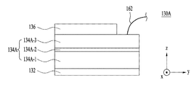
図7a〜図7cは実施例による発光素子パッケージ1000Aに含まれる発光素子130の多様な実施例130A、130B、130Cの断面図を示す。
7a-7c show cross-sectional views of various examples 130A, 130B, 130C of the
図1〜図3に示した発光素子130は、図7aに示したように、垂直型ボンディング構造を有することができる。しかし、他の実施例によると、発光素子130は、図7bに示したように、水平型ボンディング構造を有することもでき、図7cに示したように、フリップチップ型ボンディング構造を有することもできる。
The
図7a〜図7cに示した発光素子130:130A〜130Cは発光構造物134A、134B、134Cを含むことができる。
The light emitting elements 130: 130A to 130C shown in FIGS. 7a to 7c can include light emitting
相異なるボンディング構造にかかわらず、発光構造物134A、134B、134Cは第1導電型半導体層134A−1、134B−1、134C−1、活性層134A−2、134B−2、134C−2及び第2導電型半導体層134A−3、134B−3、134C−3を含むことができる。発光構造物134A、134B、134Cは互いに異なる構成物質を有することができ、これについては以下で説明する。
Regardless of the different bonding structures, the
まず、図7aに示した垂直型ボンディング構造を有する発光素子130Aは支持基板132、発光構造物134A及びオーム接触層136を含むことができる。
First, the
支持基板132は発光構造物134Aを支持する役割をし、導電型物質を含むことができる。これは、支持基板132上に配置された第1導電型半導体層134A−1が支持基板132を介して第1リードフレーム122に電気的に連結されるようにするためである。
The
例えば、支持基板132はサファイア(Al203)、GaN、SiC、ZnO、GaP、InP、Ga203、GaAs及びSiの少なくとも1種を含むことができるが、これに限られない。仮に、支持基板132が導電型の場合、支持基板132の全体は第1電極の役割をすることができるので、電気伝導度に優れた金属を使うことができ、発光素子130Aの作動時に発生する熱を充分に発散させることができなければならないので、熱伝導度が高い金属を使うことができる。このために、支持基板132は、モリブデン(Mo)、シリコン(Si)、タングステン(W)、銅(Cu)及びアルミニウム(Al)からなる群から選択される物質又はこれらの合金でなることができ、さらに金(Au)、銅合金(Cu Alloy)、ニッケル(Ni)、銅−タングステン(Cu−W)、キャリアウエハー(例:GaN、Si、Ge、GaAs、ZnO、SiGe、SiC、Ga2O3など)などを選択的に含むことができる。
For example, the
また、支持基板132が反射性物質で具現される場合、発光構造物134Aから放出されて上部又は側部に向かわなくて支持基板132に向かう光を反射させて光抽出効率を高めることができる。
Further, when the
もしくは、支持基板132と発光構造物134Aの間に反射層(図示せず)がさらに配置されることもできる。
Alternatively, a reflective layer (not shown) may be further arranged between the
反射層は活性層134A−2から放出された光を上方に反射させる役割をし、支持基板132上に配置され、約2500Åの厚さを有することができる。例えば、反射層はアルミニウム(Al)、銀(Ag)、ニッケル(Ni)、白金(Pt)、ロジウム(Rh)、又はAl、Ag、Pt又はRhを含む合金を含む金属層でなることができる。アルミニウム又は銀などは活性層134A−2で発生した光を効果的に反射して発光素子130Aの光抽出効率を大きく改善させることができる。また、このような反射層は多様な光反射パターンを有することができる。光反射パターンは半球形陽刻形態を有してもよいが、陰刻形態又はその他の多様な形態を有してもよい。
The reflective layer serves to reflect the light emitted from the
第1導電型半導体層134A−1は支持基板132上に配置される。第1導電型半導体層134A−1は第1導電型ドーパントがドープされた3族−5族化合物半導体で具現されることができ、第1導電型がn型の場合、n型ドーパントとしてSi、Ge、Sn、Se又はTeを含むことができるが、これに限定されない。
The first
第1導電型半導体層134A−1は、例えばAlxInyGa(1−x−y)N(0≦x≦1、0≦y≦1、0≦x+y≦1)の組成式を有する半導体物質を含むことができる。第1導電型半導体層134A−1はGaN、InN、AlN、InGaN、AlGaN、InAlGaN、AlInN、AlGaAs、InGaAs、AlInGaAs、GaP、AlGaP、InGaP、AlInGaP及びInPのいずれか1種以上で形成されることができる。
The first
活性層134A−2は第1導電型半導体層134A−1上に配置される。活性層134A−2は第1導電型半導体層134A−1を通じて注入される電子と第2導電型半導体層134A−3を通じて注入される正孔が互いに会って、活性層134A−2を成す物質固有のエネルギーバンドによって決定されるエネルギーを有する光を放出する層である。
The
活性層134A−2は、単一井戸構造、多重井戸構造、単一量子井戸構造、多重量子井戸構造(MQW:Multi Quantum Well)、量子細線(Quantum−Wire)構造、又は量子ドット(Quantum Dot)構造の少なくとも一つに形成されることができる。
The
活性層134A−2の井戸層/障壁層はInGaN/GaN、InGaN/InGaN、GaN/AlGaN、InAlGaN/GaN、GaAs(InGaAs)/AlGaAs及びGaP(InGaP)/AlGaPのいずれか1種以上のペア構造に形成されることができるが、これに限定されない。井戸層は障壁層のバンドギャップより小さなバンドギャップを有する物質で形成されることができる。
The well layer / barrier layer of the
活性層134A−2の上又は/及び下には導電型クラッド層(図示せず)が形成されることができる。導電型クラッド層は活性層134A−2の障壁層のバンドギャップより広いバンドギャップを有する半導体で形成されることができる。例えば、導電型クラッド層はGaN、AlGaN、InAlGaN又は超格子構造などを含むことができる。また、導電型クラッド層はn型又はp型でドープされることができる。
A conductive clad layer (not shown) can be formed above and / below the
第2導電型半導体層134A−3は活性層134A−2上dに配置される。第2導電型半導体層134A−3は半導体化合物で形成されることができる。第2導電型半導体層134A−3は3族−5族、2族−6族などの化合物半導体で具現されることができ、例えばInxAlyGa1−x−yN(0≦x≦1、0≦y≦1、0≦x+y≦1)の組成式を有する半導体物質を含むことができる。仮に、第2導電型がp型の場合、第2導電型半導体層134A−3はp型ドーパントとして、Mg、Zn、Ca、Sr、Baなどを含むことができる。
The second
オーム接触層136は第2導電型半導体層134A−3上に配置される。第2導電型半導体層134A−3がp型半導体層の場合、不純物ドーピング濃度が低くて接触抵抗が高く、それによってオーム特性が良くないことがあるので、このようなオーム特性を改善するために、発光素子130Aはオーム接触層136をさらに含むことができる。第2導電型半導体層134A−3上に配置されるオーム接触層136は金属及び透明な伝導酸化膜(TCO:Transparent Conductive Oxide)の少なくとも一つを含むことができる。例えば、オーム接触層136は約200Åの厚さを有することができ、ITO(indium tin oxide)、IZO(indium zinc oxide)、IZTO(indium zinc tin oxide)、IAZO(indium aluminum zinc oxide)、IGZO(indium gallium zinc oxide)、IGTO(indium gallium tin oxide)、AZO(aluminum zinc oxide)、ATO(antimony tin oxide)、GZO(gallium zinc oxide)、IZON(IZO Nitride)、AGZO(Al−Ga ZnO)、IGZO(In−Ga ZnO)、ZnO、IrOx、RuOx、NiO、RuOx/ITO、Ni/IrOx/Au、及びNi/IrOx/Au/ITO、Ag、Ni、Cr、Ti、Al、Rh、Pd、Ir、Sn、In、Ru、Mg、Zn、Pt、Au及びHfの少なくとも1種を含んで形成されることができるが、このような材料に限定されない。
The
図1〜図3の場合、発光素子130Aが第1リードフレーム122上に配置されたものとして示されているが、実施例はこれに限られない。すなわち、他の実施例によると、発光素子130Aは第2リードフレーム124上に配置されることもできる。
In the case of FIGS. 1 to 3, the
また、前述したように、第1導電型半導体層134A−1は支持基板132を介して第1リードフレーム122に電気的に連結されるので、ワイヤが必要ではない。すなわち、支持基板132は第1電極の役割をすることができる。一方、第2導電型半導体層134A−3は第1ワイヤ162によって第2リードフレーム124に電気的に連結されることができる。
Further, as described above, since the first
図1〜図3及び図7aに示した第1ワイヤ162は第2導電型半導体層134A−3に直接連結されたものとして示されているが、実施例はこれに限られない。すなわち、他の実施例によると、第1ワイヤ162はオーム接触層136を介して第2導電型半導体層134A−3に電気的に連結されることもできる。この場合、オーム接触層136は第2電極の役割をすることができる。
The
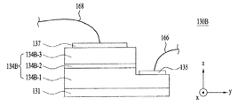
次に、図7bに示した水平型ボンディング構造を有する発光素子130Bは、基板131、発光構造物134B及び第1及び第2電極135、137を含むことができる。
Next, the
基板131は導電型物質又は非導電型物質を含むことができる。例えば、基板131はサファイア(Al203)、GaN、SiC、ZnO、GaP、InP、Ga203、GaAs及びSiの少なくとも1種を含むことができる。
The
例えば、基板131がシリコン基板の場合、(111)結晶面を主面として有することができる。シリコン基板の場合、大口径が容易で熱伝導度に優れるが、シリコンと窒化物系発光構造物134B間の熱膨張係数の差及び格子不整合によって発光構造物134Bでクラック(crack)が発生するなどの問題点が発生することもある。
For example, when the
これを防止するために、基板131と発光構造物134Bの間にバッファー層(又は、転移層)(図示せず)が配置されることができる。バッファー層は、例えばAl、In、N及びGaからなる群から選択される少なくとも1種の物質を含むことができるが、これに限られない。また、バッファー層は単層又は多層構造を有することもできる。
In order to prevent this, a buffer layer (or transition layer) (not shown) can be arranged between the
第1導電型半導体層134B−1は基板131上に配置される。第1導電型半導体層134B−1は第1導電型ドーパントがドープされたIII−V族又はII−VI族などの化合物半導体で具現されることができ、第1導電型ドーパントがドープされることができる。第1導電型半導体層134B−1がn型半導体層の場合、第1導電型ドーパントはn型ドーパントとして、Si、Ge、Sn、Se又はTeを含むことができるが、これに限定されない。
The first
例えば、第1導電型半導体層134B−1はAlxInyGa(1−x−y)N(0≦x≦1、0≦y≦1、0≦x+y≦1)の組成式を有する半導体物質を含むことができる。第1導電型半導体層134B−1はGaN、InN、AlN、InGaN、AlGaN、InAlGaN、AlInN、AlGaAs、InGaAs、AlInGaAs、GaP、AlGaP、InGaP、AlInGaP及びInPのいずれか1種以上を含むことができる。
For example, the first
活性層134B−2は第1導電型半導体層134B−1上に配置される。活性層134B−2は第1導電型半導体層134B−1を通じて注入される電子(又は、正孔)と第2導電型半導体層134B−3を通じて注入される正孔(又は、電子)が互いに会って、活性層134B−2を成す物質固有のエネルギーバンドによって決定されるエネルギーを有する光を放出する層である。
The
活性層134B−2は単一井戸構造、多重井戸構造、単一量子井戸構造、多重量子井戸構造(MQW:Multi Quantum Well)、量子細線(Quantum−Wire)構造、又は量子ドット(Quantum Dot)構造の少なくとも一つに形成されることができる。
The
活性層134B−2の井戸層/障壁層はInGaN/GaN、InGaN/InGaN、GaN/AlGaN、InAlGaN/GaN、GaAs(InGaAs)/AlGaAs及びGaP(InGaP)/AlGaPのいずれか1種以上のペア構造に形成されることができるが、これに限定されない。井戸層は障壁層のバンドギャップエネルギーより低いバンドギャップエネルギーを有する物質で形成されることができる。
The well layer / barrier layer of the
活性層134B−2の上又は/及び下には導電型クラッド層(図示せず)が形成されることができる。導電型クラッド層は活性層134B−2の障壁層のバンドギャップエネルギーより高いバンドギャップエネルギーを有する半導体で形成されることができる。例えば、導電型クラッド層はGaN、AlGaN、InAlGaN又は超格子構造などを含むことができる。また、導電型クラッド層はn型又はp型でドープされることができる。
A conductive clad layer (not shown) can be formed above and / below the
第2導電型半導体層134B−3は活性層134B−2上に配置される。第2導電型半導体層134B−3は半導体化合物で形成されることができ、III−V族又はII−VI族などの化合物半導体で具現されることができる。例えば、第2導電型半導体層134B−3はInxAlyGa1−x−yN(0≦x≦1、0≦y≦1、0≦x+y≦1)の組成式を有する半導体物質を含むことができる。第2導電型半導体層134B−3には第2導電型ドーパントがドープされることができる。第2導電型半導体層134B−3がp型半導体層の場合、第2導電型ドーパントはp型ドーパントとして、Mg、Zn、Ca、Sr、Baなどを含むことができる。
The second
第1電極135は第2導電型半導体層134B−3と活性層134B−2と第1導電型半導体層134B−1の一部をメサ食刻して露出された第1導電型半導体層134B−1上に配置される。第2電極137は第2導電型半導体層134B−3上に配置される。例えば、アルミニウム(Al)、チタン(Ti)、クロム(Cr)、ニッケル(Ni)、銅(Cu)及び金(Au)の少なくとも1種を含んで単層又は多層構造に第1及び第2電極135、137を形成することができる。
The
第1電極135が第1ワイヤ166によって第1リードフレーム122に電気的に連結されることにより、第1導電型半導体層134B−1は第1リードフレーム122に電気的に連結されることができる。また、第2電極137が第2ワイヤ168によって第2リードフレーム124に電気的に連結されることにより、第2導電型半導体層134B−3は第2リードフレーム124に電気的に連結されることができる。
By electrically connecting the
次に、図7cに示したフリップチップ型ボンディング構造を有する発光素子130Cは基板131、発光構造物134C、第1電極135及び第2電極137を含むことができる。
Next, the
基板131の下に発光構造物134Cが配置されることができる。第1導電型半導体層134C−1は基板131の下に配置される。活性層134C−2は第1導電型半導体層134C−1の下に配置される。第2導電型半導体層134C−3は活性層134C−2の下に配置される。第1電極135は第1導電型半導体層134C−1の下に配置される。第2電極137は第2導電型半導体層134C−3の下に配置される。
The
図7cに示した基板131、第1導電型半導体層134C−1、活性層134C−2、第2導電型半導体層134C−3、第1電極135及び第2電極137は図7bに示した基板131、第1導電型半導体層134B−1、活性層134B−2、第2導電型半導体層134B−3、第1電極135及び第2電極137のそれぞれと同一の役割をすることができ、同一の物質で具現されることができる。ただ、図7bに示した発光素子130Bの場合、光が上部と側部の方向に放出されるので、第2導電型半導体層134B−3と第2電極137のそれぞれは光透過性物質で具現されることができる。これとは違い、図7cに示した発光素子130Cの場合、光が上部と側部の方向に放出されるので、第1導電型半導体層134C−1、基板131及び第1電極135のそれぞれは光透過性物質で具現されることができる。
The
図7cに示したように、発光素子130Cがフリップチップ型ボンディング構造を有する場合、発光素子パッケージ1000Aは第1及び第2半田部139A、139Bをさらに含むことができる。
As shown in FIG. 7c, when the
第1半田部139Aは第1電極135と第1リードフレーム122の間に配置される。したがって、第1導電型半導体層134C−1は第1電極135及び第1半田部139Aを介して第1リードフレーム122と電気的に連結されることができる。第2半田部139Bは第2電極137と第2リードフレーム124の間に配置される。したがって、第2導電型半導体層134C−3は第2電極137及び第2半田部139Bを介して第2リードフレーム124と電気的に連結されることができる。
The
図7a〜図7cに示した発光構造物134A、134B、134Cのそれぞれにおいて、第1導電型半導体層134A−1、134B−1、134C−1はp型半導体層で、第2導電型半導体層134A−3、134B−3、134C−3はn型半導体層で具現することができる。もしくは、第1導電型半導体層134A−1、134B−1、134C−1はn型半導体層で、第2導電型半導体層134A−3、134B−3、134C−3はp型半導体層で具現することもできる。
In the
発光構造物134A、134B、134Cはn−p接合構造、p−n接合構造、n−p−n接合構造及びp−n−p接合構造のいずれか一構造に具現することができる。
The
一方、図1〜図3を再び参照すると、モールディング部材140は発光素子130を取り囲むように胴体110及び第1及び第2リードフレーム122、124上に配置されることができる。モールディング部材140は発光素子130を取り囲んで保護することができる。また、モールディング部材140は蛍光体を含み、発光素子130から放出された光の波長を変化させることができる。
On the other hand, referring to FIGS. 1 to 3 again, the
モールディング部材140は第1及び第2モールディング部材142、144を含むことができる。
The
第1モールディング部材142は発光素子130の側部を取り囲み、第1及び第2リードフレーム122、124上に配置されることができる。第1モールディング部材142は発光素子130から放出される光の光束を向上させ、外部の環境から発光素子130が損傷(damage)することを防止する役割をする。
The
第2モールディング部材144は発光素子130の上部を取り囲み、第1モールディング部材142上に配置されることができる。第2モールディング部材144は発光素子130から放出される光の光束を2次に向上させる役割をする。また、図1〜図3に示した第1及び第3ワイヤ162、164は第2モールディング部材144まで配置されずに第1モールディング部材142の内部にのみ配置されることもでき、設計によって、第1ワイヤ162、166、第2ワイヤ168及び第3ワイヤ164のそれぞれは第1モールディング部材142だけでなく第2モールディング部材144の内部まで伸びて配置されることができる。この場合、第2モールディング部材144は第1ワイヤ162、166、第2ワイヤ168及び第3ワイヤ164のそれぞれを保護する役割をすることができる。
The
モールディング部材140はシリコーンで具現されることができる。この場合、第1モールディング部材142はホワイトシリコーン(white silicone)で具現され、第2モールディング部材144はクリアシリコーン(clear silicone)で具現されることができるが、実施例はモールディング部材140の特定の材質に限られない。
The
第1モールディング部材142の第3厚さT3と発光素子130の第4厚さT4は互いに同一であっても違ってもよい。例えば、図2に示したように、第3厚さT3は第4厚さT4と同一であってもよい。
The third thickness T3 of the
一方、ツェナーダイオード150は第1又は第2リードフレーム122、124のうち発光素子130が配置されていない他の一つのリードフレーム上に配置されることができる。例えば、図1〜図3に例示したように、発光素子130が垂直型ボンディング構造を持って第1リードフレーム122上に配置される場合、ツェナーダイオード150は第2リードフレーム124上に配置されることができる。ここで、ツェナーダイオード150と第1リードフレーム122は第3ワイヤ164を介して互いに電気的に連結されることができる。
On the other hand, the
前述した第1ワイヤ162、166、第2ワイヤ168及び第3ワイヤ164のそれぞれは金(Au)で具現されることができる。
Each of the
ツェナーダイオード150は発光素子パッケージ1000Aに流れる過電流又は印加される電圧ESD(ElectroStatic Discharge)を防止する役割をする。
The
また、接着層152はツェナーダイオード150と第2リードフレーム124の間に配置されることができる。接着層152はツェナーダイオード150を第2リードフレーム124にボンディングさせる役割をし、一種のペースト(paste)形態を有し、銀(Ag)とエポキシ(epoxy)を含むことができる。
Further, the
場合によって、発光素子パッケージ1000Aはツェナーダイオード150及び接着層152を含まないこともあり、実施例はこれらのツェナーダイオード150及び接着層152の形態又は存在有無に限られない。
In some cases, the light emitting
図8は他の実施例による発光素子パッケージ1000Bの断面図を示す。
FIG. 8 shows a cross-sectional view of the light emitting
図8に示した発光素子パッケージ1000Bは、胴体110、第1及び第2リードフレーム122、124、発光素子130、モールディング部材140、ツェナーダイオード150、接着層152、第1及び第3ワイヤ162及び164及びダム(dam)170を含むことができる。
The light emitting
図8に示した発光素子パッケージ1000Bは、ダム170をさらに含むことを除けば、図3に示した発光素子パッケージ1000Aと同一である。よって、図8に示した発光素子パッケージ1000Bにおいて図3に示した発光素子パッケージ1000Aと同一の部分に対しては同一の参照符号を付け、重複説明を省略する。
The light emitting
図8に示したダム170は第1及び第2リードフレーム122、124上に配置されたモールディング部材140を閉じこめる役割をする。すなわち、ダム170と第1及び第2リードフレーム122、124の上部面122HT、124HTがなすキャビティにモールディング部材140が配置されることができる。
The
以下、図3に示した実施例による発光素子パッケージ1000Aの製造方法を図9a〜図9dに基づいて以下で説明する。しかし、実施例による発光素子パッケージ1000Aは図9a〜図9dに示したものとは違う製造方法でも製造することができるのは言うまでもない。また、図8に示した発光素子パッケージ1000Bの場合にも、ダム170がさらに形成されることを除けば、図9a〜図9dに示した方法で製造することができるのは言うまでもない。
Hereinafter, a method for manufacturing the light emitting
図9a〜図9dは実施例による発光素子パッケージ1000Aの製造方法を説明するための工程断面図を示す。
9a to 9d show cross-sectional views of a process for explaining a method of manufacturing the light emitting
図9aを参照すると、胴体110と第1及び第2リードフレーム122、124を形成する。ここで、胴体110はブラックEMCから製造され、第1及び第2リードフレーム122、124のそれぞれは銅(Cu)から製造されることができる。
With reference to FIG. 9a, the
例えば、銅をエッチング(etching)及びスタンピング(stamping)して第1及び第2リードフレーム122、124のパターンを先に形成する。その後、パターニングされた第1及び第2リードフレーム122、124にブラックEMCを射出成形(injection molding)することによって胴体110を形成することができる。
For example, copper is etched and stamped to first form the patterns of the first and second lead frames 122, 124. After that, the
その後、第1リードフレーム122上に発光素子130をダイボンディング(die bonding)する。例えば、発光素子130は図7aに示したような構造に次のように形成されることができる。
After that, the
第1リードフレーム122上に支持基板132を形成し、支持基板132上に発光構造物134Aを形成する。第1導電型半導体層134A−1のための第1物質層、活性層134A−2のための第2物質層、第2導電型半導体層134A−3のための第3物質層を支持基板132上に順次形成する。
The
第1物質層は3族−5族、2族−6族などの化合物半導体で具現されることができ、例えばAlxInyGa(1−x−y)N(0≦x≦1、0≦y≦1、0≦x+y≦1)の組成式を有する半導体物質を含むことができる。第2物質層はペア構造に繰り返される井戸層/障壁層を含むことができ、井戸層/障壁層はInGaN/GaN、InGaN/InGaN、GaN/AlGaN、InAlGaN/GaN、GaAs(InGaAs)/AlGaAs及びGaP(InGaP)/AlGaPのいずれか1種を含むことができる。第3物質層は3族−5族、2族−6族などの化合物半導体で具現されることができ、例えばInxAlyGa1−x−yN(0≦x≦1、0≦y≦1、0≦x+y≦1)の組成式を有する半導体物質を含むことができる。 The first material layer can be embodied in a compound semiconductor such as Group 3-5, Group 2-6, and for example, Al x In y Ga (1-xy) N (0 ≦ x ≦ 1, 0). A semiconductor material having a composition formula of ≦ y ≦ 1 and 0 ≦ x + y ≦ 1) can be included. The second material layer can include a well layer / barrier layer that repeats in a pair structure, and the well layer / barrier layer includes InGaN / GaN, InGaN / InGaN, GaN / AlGaN, InAlGaN / GaN, GaAs (InGaAs) / AlGaAs, and so on. Any one of GaP (InGaP) / AlGaP can be included. The third material layer is a Group III-V, it is embodied in a compound semiconductor such as a Group 2 -6 group that can, for example, In x Al y Ga 1-x -y N (0 ≦ x ≦ 1,0 ≦ y A semiconductor material having a composition formula of ≦ 1, 0 ≦ x + y ≦ 1) can be included.
その後、第1〜第3物質層を通常の写真食刻工程でパターニングして発光構造物134を形成することができる。その後、発光構造物134上にオーム接触層136を形成する。
After that, the first to third material layers can be patterned by a normal photographic engraving process to form the
この時、発光素子130が形成されるうちに接着層152とツェナーダイオード150を第2リードフレーム124上に形成することができる。
At this time, the
その後、図9bを参照すると、発光素子130をワイヤボンディング(Wire bonding)する。すなわち、発光素子130の第2導電型半導体層134A−3と第2リードフレーム124を電気的に連結する第1ワイヤ162を形成し、ツェナーダイオード150を第1リードフレーム122と電気的に連結する第3ワイヤ164を形成する。
Then, referring to FIG. 9b, the
その後、図9cを参照すると、胴体110と第1及び第2リードフレーム122、124の側部にダム210を形成することで、モールディング部材140が収容されるキャビティを形成するダム工程を進める。このように、ダム工程を行う理由は、流動性(又は、粘性)を有する第1及び第2モールディング部材142、144が硬化する前に流れないようにするためである。
After that, referring to FIG. 9c, the dam step of forming the cavity in which the
その後、図9dに示したように、ダム210、第1及び第2リードフレーム122、124及び胴体110によって形成される空間にモールディング部材140を満たすディスペンシング(dispensing)工程を進める。この時、第1モールディング部材142を発光素子130の高さまで形成した後、第2モールディング部材144を発光素子130の上部面と第1モールディング部材142上に形成する。前述したように、ダム210が配置されることにより、ディスペンスされたモールディング部材140が硬化する前に流れることがない。
Then, as shown in FIG. 9d, a dispensing step of filling the space formed by the
その後、図9dに示したダム210を除去すれば、図3に示した発光素子パッケージ1000Aが出来上がることができる。図9a〜図9dは一つの発光素子パッケージ1000Aを製造する工程断面図であるが、複数の発光素子パッケージ1000Aが図9a〜図9dに示した工程によって同時に形成されることができる。この場合、図9dに示したような工程後、ダイシング(dicing)工程を行って単一発光素子パッケージ1000Aに分離することができる。
After that, if the
以下、ブラックEMCで具現された胴体110を有する実施例による発光素子パッケージ1000A、1000Bとホワイト(white)EMC、PCT(polycyclohexylene−dimethylene terephthalates)のようなセラミック、又はAlNで具現された基板を有する比較例による発光素子パッケージを次のように比較する。また、比較例による発光素子パッケージは、たとえ図示されてはいないが、説明の便宜上、実施例による発光素子パッケージ1000A、1000Bにおいて胴体110の代わりに基板を含むと仮定する。
Below, a comparison with light emitting device packages 1000A, 1000B according to an embodiment having a
比較例による発光素子パッケージのように、基板をホワイトEMC、セラミック又はAlNで具現する場合、多様な問題が生じることがある。 When the substrate is embodied in white EMC, ceramic or AlN as in the light emitting device package according to the comparative example, various problems may occur.
例えば、比較例による発光素子パッケージの製造コストより実施例による発光素子パッケージ1000A、1000Bの製造コストがずっと低い。何故ならば、セラミック又はAlNの値段はブラックEMCより10倍〜30倍程度高いからである。 For example, the manufacturing cost of the light emitting element packages 1000A and 1000B according to the embodiment is much lower than the manufacturing cost of the light emitting element package according to the comparative example. This is because the price of ceramic or AlN is about 10 to 30 times higher than that of black EMC.
また、比較例による発光素子パッケージがPCT又はホワイトEMCで具現された基板を有する場合、発光素子パッケージの剛性、射出性、工程性が不安になることがある。一方、実施例による発光素子パッケージ1000A、1000Bは胴体110をブラックEMCで具現することにより、このような不安な問題を解消することができる。
Further, when the light emitting element package according to the comparative example has a substrate embodied in PCT or white EMC, the rigidity, ejection property, and processability of the light emitting element package may become uncertain. On the other hand, in the light emitting element packages 1000A and 1000B according to the embodiment, such an uneasy problem can be solved by embodying the
また、ブラックEMC又はホワイトEMCは粒子を含み、ブラックEMCに含まれた粒子はホワイトEMCに含まれた粒子よりもっと小さい。よって、実施例による発光素子パッケージ1000A、1000Bのように胴体110をブラックEMCで製造する場合、第1及び第2リードフレーム122、124の集積度が増加して、単位時間当たり製造可能な発光素子パッケージの個数を増加させることができる。さらに、粒子の大きさが小さくなる場合、発光素子パッケージ1000A、1000Bを多様な形態に設計することができるなど、設計の自由度が増加することができる。
Further, the black EMC or the white EMC contains particles, and the particles contained in the black EMC are much smaller than the particles contained in the white EMC. Therefore, when the
また、比較例による発光素子パッケージは発光素子130から第1及び第2リードフレーム122、124までの熱抵抗(thermal resistance)が7.5℃/Wである。一方、実施例によると、胴体110をブラックEMCで具現する場合、発光素子130から第1及び第2リードフレーム122、124の下端(122Lの底面又は124Lの底面)までの熱抵抗は5℃/Wと相対的に小さい。よって、同じ電力で、ブラックEMCで具現された胴体110を有する発光素子パッケージ1000A、1000Bはセラミック又はAlNなどで具現された基板を有する比較例による発光素子パッケージより相対的に熱伝導が早くて優れた放熱特性を有する。
Further, the light emitting element package according to the comparative example has a thermal resistance of 7.5 ° C./W from the
また、比較例による発光素子パッケージのように基板をホワイトEMC又はセラミックで具現する場合、基板にクラック(crack)が発生することがあるだけではなく、製造工程上粉塵が発生して発光素子パッケージの性能に悪影響を及ぼすことがある。しかし、実施例による発光素子パッケージのように胴体110をブラックEMCで具現する場合、このようなクラックと粉塵発生を防止することができる。
Further, when the substrate is embodied in white EMC or ceramic as in the light emitting element package according to the comparative example, not only cracks may occur in the substrate, but also dust is generated in the manufacturing process to generate the light emitting element package. May adversely affect performance. However, when the
また、比較例による発光素子パッケージの基板は樹脂などで具現されるので、コップ形態を有し、その上部面が平らな断面形状を有することができない。しかし、基板をセラミックで具現する場合、基板の上部面は平らな断面形状を有してもよいが、セラミックは前述したようにブラックEMCと比較すると多様な問題点がある。一方、実施例による発光素子パッケージ1000A、1000Bの場合、セラミックより安いブラックEMCを使って価格を減らしながらも胴体110の上部面110Tを図6に例示したように平らに形成することができる。
Further, since the substrate of the light emitting element package according to the comparative example is embodied in a resin or the like, it cannot have a cup shape and its upper surface cannot have a flat cross-sectional shape. However, when the substrate is embodied in ceramic, the upper surface of the substrate may have a flat cross-sectional shape, but ceramic has various problems as compared with black EMC as described above. On the other hand, in the case of the light emitting element packages 1000A and 1000B according to the embodiment, the
以下、さらに他の実施例による発光素子パッケージ1000C、1000Dを添付図面に基づいて次のように説明する。 Hereinafter, the light emitting element packages 1000C and 1000D according to still another embodiment will be described as follows based on the accompanying drawings.
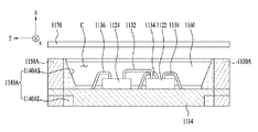
図10はさらに他の実施例による発光素子パッケージ1000Cの上部結合斜視図を示し、図11は図10に示した発光素子パッケージ1000Cの上部分解斜視図を示し、図12は図10に示した発光素子パッケージ1000Cの下部分解斜視図を示し、図13は図10に示した発光素子パッケージ1000Cの平面図を示し、図14は図10に示した発光素子パッケージ1000Cの底面図を示し、図15は図10に示した発光素子パッケージ1000Cの上部部分結合斜視図を示し、図16及び図17は図10に示した発光素子パッケージ1000Cの断面図を示す。
FIG. 10 shows an upper coupled perspective view of the light emitting
図10〜図17を参照すると、さらに他の実施例による発光素子パッケージ1000Cは、第1及び第2リードフレーム1112、1114、光源1122、1124、ツェナーダイオード1126、第1〜第4ワイヤ1132〜1138、内側胴体1140A、外側胴体1150A、モールディング部材1160及び上部構造物1170を含むことができる。図10〜図15で、モールディング部材1160と上部構造物1170の図示は省略した。
Referring to FIGS. 10 to 17, the light emitting
内側胴体1140Aは第1及び第2リードフレーム1112、1114を互いに電気的に分離させ、第1及び第2リードフレーム1112、1114と一緒にキャビティ(C:Cavity)を定義することができる。
The
また、内側胴体1140Aは下部1140AL及び側部1140ASを含むことができる。ここで、内側胴体1140Aの下部1140ALは第1及び第2リードフレーム1112、1114を互いに電気的に離隔させる役割をする。このために、第1及び第2リードフレーム1112、1114の間に内側胴体1140Aの下部1140ALが配置されることができる。内側胴体1140Aの側部1140ASは下部1140ALから伸びてキャビティCの側面を形成することができる。
Further, the
内側胴体1140Aの側部1140ASが傾斜面を有する場合、光源1122、1124から放出される光が傾斜面で反射されて上方に進行することによって光抽出効率を高めることができる。
When the side portion 1140AS of the
図18はさらに他の実施例による発光素子パッケージ1000Dの上部結合斜視図を示し、図19は図18に示した発光素子パッケージ1000Dの上部部分結合斜視図を示す。
FIG. 18 shows an upper coupled perspective view of the light emitting
内側胴体1140A、1140Bは外側胴体1150A、1150Bの上部面を貫通する反射突出部1140AP、1140BPをさらに含むことができる。例えば、図10〜図15に例示したように、反射突出部1140APは発光素子パッケージ1000Cの第1外方向(例えば、x軸方向)に突出して外側胴体1150Aの上部面を2等分することができる。もしくは、図18及び図19に示したように、反射突出部1140BPは第2外方向(例えば、x軸とy軸方向)に突出して外側胴体1150Bの上部面を4等分することもできる。しかし、実施例はこれに限られない。すなわち、他の実施例によると、内側胴体1140A、1140Bは外側胴体1150A、1150Bの上部面を3等分するとか5等分以上することができるのは言うまでもない。
The
図10〜図19に例示した反射突出部1140AP、1140BPは対称の平面形状を有してもよい。すなわち、図10〜図15に示した反射突出部1140APはx軸方向に対称の平面形状を有し、図18及び図19に示した反射突出部1140BPはx軸方向及びy軸方向に対称の平面形状を有してもよい。 The reflective protrusions 1140AP and 1140BP illustrated in FIGS. 10 to 19 may have a symmetrical planar shape. That is, the reflection protrusion 1140AP shown in FIGS. 10 to 15 has a planar shape symmetrical in the x-axis direction, and the reflection protrusion 1140BP shown in FIGS. 18 and 19 is symmetrical in the x-axis direction and the y-axis direction. It may have a planar shape.
図10〜図15に示した反射突出部1140APと違う形態の反射突出部1140BPを有する相違点を除けば、図18及び図19に示した発光素子パッケージ1000Dは図10〜図17に示した発光素子パッケージ1000Cと同一である。したがって、以下で図18及び図19に示した発光素子パッケージ1000Dに対しては図10〜図17に示した発光素子パッケージ1000Cについての説明を適用することができる。
Except for the difference that the reflection protrusion 1140AP shown in FIGS. 10 to 15 and the reflection protrusion 1140BP having a different form from the reflection protrusion 1140AP, the light emitting
内側胴体1140Aの下部1140ALは複数の貫通孔を含むことができる。例示したように、内側胴体1140Aの下部1140ALは第1〜第3貫通孔TH1、TH2、TH3を含むことができる。
The lower portion 1140AL of the
第1及び第2リードフレーム1112、1114は、前述したように、内側胴体1140Aによって互いに電気的に離隔することができる。第1及び第2リードフレーム1112、1114は光源1122、1124に電源を提供する役割をする。また、第1及び第2リードフレーム1112、1114は光源1122、1124で発生した光を反射させて光効率を高める役割をすることもでき、光源1122、1124で発生した熱を外部に排出させる役割もすることができる。
The first and second lead frames 1112 and 1114 can be electrically separated from each other by the
第1リードフレーム1112は第1下側リードフレーム1112B及び第1上側リードフレーム1112Tを含むことができる。第1下側リードフレーム1112Bは複数の貫通孔の一部(例えば、第1貫通孔TH1)に挿入されて配置されることができる。第1上側リードフレーム1112Tは第1下側リードフレーム1112B上に配置され、キャビティCの底面の一部を形成することができる。
The
また、第1下側リードフレーム1112Bと第1上側リードフレーム1112Tは例示したように互いに別個であってもよく、例示したものとは違って一体型であってもよい。
Further, the first
第1貫通孔TH1に挿入される第1下側リードフレーム1112Bとは違い、第1上側リードフレーム1112Tは第1貫通孔TH1に挿入されなくてもよいが、実施例はこれに限られない。第1上側リードフレーム1112Tは第1下側リードフレーム1112Bより広い平面積を有することができるが、実施例はこれに限られない。
Unlike the first
また、第2リードフレーム1114は第2下側リードフレーム1114B及び第2上側リードフレーム1114Tを含むことができる。第2下側リードフレーム1114Bは複数の貫通孔の残り(例えば、第2及び第3貫通孔TH2、TH3)に挿入されて配置されることができる。特に、図12を参照すると、第2下側リードフレーム1114Bは互いに別個である第2−1下側リードフレーム1114B1及び第2−2下側リードフレーム1114B2を含むことができる。第2−1下側リードフレーム1114B1は第2貫通孔TH2に挿入されて配置され、第2−2下側リードフレーム1114B2は第3貫通孔TH3に挿入されて配置されることができる。しかし、実施例はこれに限られない。他の実施例によると、図12に示したものとは違い、第2下側リードフレーム1114Bは一つであってもよい。すなわち、第2−1及び第2−2下側リードフレーム1114B1、1114B2は一体型であってもよい。仮に、第2−1及び第2−2下側リードフレーム1114B1、1114B2が一体型の場合、第2及び第3貫通孔TH2、TH3が互いに統合された貫通孔(図示せず)に一体型の第2下側リードフレーム1114Bが挿入されて配置されることができる。
Further, the
第2上側リードフレーム1114Tは第2下側リードフレーム1114B上に配置され、キャビティCの底面の残りを形成することができる。
The second
また、第2下側リードフレーム1114Bと第2上側リードフレーム1114Tは例示したように互いに別個であってもよく、例示したものとは違って一体型であってもよい。
Further, the second
第2及び第3貫通孔TH2、TH3にそれぞれ挿入される第2−1及び第2−2下側リードフレーム1114B1、1114B2とは違い、第2上側リードフレーム1114Tは第2及び第3貫通孔TH2、TH3に挿入されなくてもよいが、実施例はこれに限られない。第2上側リードフレーム1114Tは第2下側リードフレーム1114Bより広い平面積を有することができるが、実施例はこれに限られない。
Unlike the second and second lower lead frames 1114B1 and 1114B2, which are inserted into the second and third through holes TH2 and TH3, respectively, the second
図15を参照すると、第1上側リードフレーム1112Tと第2上側リードフレーム1114Tと内側胴体1140Aの下部1140ALはキャビティCの底面に相当する同一水平面を形成することができる。
Referring to FIG. 15, the first
第1及び第2リードフレーム1112、1114のそれぞれは電気伝導性を有する物質で具現されることができるが、実施例は第1及び第2リードフレーム1112、1114の特定の材質に限られない。第1及び第2リードフレーム1112、1114のそれぞれは銅(Cu)、ニッケル(Ni)、銀(Ag)又は金(Au)の少なくとも1種を含むことができる。例えば、第1及び第2リードフレーム1112、1114のそれぞれのベース(base)物質は銅(Cu)であり、ベースの粗い部分を1次的に銅(Cu)又はニッケル(Ni)で下地メッキ(strike)した後、銀(Ag)又は金(Au)でメイン(main)メッキすることにより、第1及び第2リードフレーム1112、1114のそれぞれを形成することができる。ここで、下地メッキとは、第1及び第2リードフレーム1112、1114のベースの表面は谷と山が繰り返される粗い面であるので、谷を銅(Cu)又はニッケル(Ni)で満たす工程を意味する。 Each of the first and second lead frames 1112 and 1114 can be embodied in a material having electrical conductivity, but the examples are not limited to the specific materials of the first and second lead frames 1112 and 1114. Each of the first and second lead frames 1112 and 1114 can contain at least one of copper (Cu), nickel (Ni), silver (Ag) or gold (Au). For example, the base material of the first and second lead frames 1112 and 1114 is copper (Cu), and the rough portion of the base is primarily plated with copper (Cu) or nickel (Ni). After striking), the first and second lead frames 1112 and 1114 can be formed by main plating with silver (Ag) or gold (Au). Here, the base plating is a step of filling the valleys with copper (Cu) or nickel (Ni) because the surface of the bases of the first and second lead frames 1112 and 1114 is a rough surface in which valleys and peaks are repeated. means.
ここで、第1下側リードフレーム1112Bと第2下側リードフレーム1114Bは発光素子パッケージ1000Cの下部に配置されるプリント基板(図示せず)に実装されることができる。
Here, the first
一方、光源1122、1124はキャビティC内で第1又は第2リードフレーム1112、1114の少なくとも1ヶ所に配置されることができる。
On the other hand, the
ここで、光源1122、1124は発光ダイオード(LED:Light Emitting Diode)であってもよく、レーザーダイオード(LD:Laser Diode)であってもよいが、実施例は光源1122、1124の形態に限られない。ここで、光源1122、1124は前述した一実施例の発光素子130:130A、130B、130Cに相当する。
Here, the
また、図10〜図19の場合、2個の光源1122、1124が配置されたものとして例示されているが、実施例は光源1122、1124の個数に限られない。すなわち、他の実施例によると、一つの光源のみ配置されることもでき、3個以上の光源が配置されることもできる。
Further, in the case of FIGS. 10 to 19, two
図10〜図19に示したように、光源1122、1124のそれぞれは水平型ボンディング構造を有することができるが、実施例はこれに限られない。すなわち、他の実施例によると、光源1122、1124のそれぞれは垂直型ボンディング構造又はフリップチップ型ボンディング構造を有することができる。
As shown in FIGS. 10 to 19, each of the
図1〜図19の場合、光源1122、1124が第2リードフレーム1114上に配置されたものとして示されているが、実施例はこれに限られない。すなわち、他の実施例によると、光源1122、1124は第1リードフレーム1112上に配置されることもできる。
In the case of FIGS. 1 to 19, the
図20a〜図20cは実施例による発光素子パッケージ1000C、1000Dに含まれる光源1122、1124のそれぞれの多様な実施例1200A、1200B、1200Cの断面図を示す。
20a-20c show cross-sectional views of various examples 1200A, 1200B and 1200C of the
図10〜図19に示した光源1122、1124のそれぞれは、図20aに示したように、水平型ボンディング構造を有することができる。しかし、他の実施例によると、光源1122、1124のそれぞれは、図20bに示したように、垂直型ボンディング構造を有することもでき、図20cに示したように、フリップチップ型ボンディング構造を有することもできる。
Each of the
図20a〜図20cに示した光源1200A、1200B、1200Cは発光構造物1220A、1250、1220Bを含むことができる。
The
相異なるボンディング構造にかかわらず、発光構造物1220A、1250、1220Bは第1導電型半導体層1222A、1252、1222B、活性層1224A、1254、1224B及び第2導電型半導体層1226A、1256、1226Bを含むことができる。発光構造物1220A、1250、1220Bは互いに同一であるとか又は互いに違う構成物質を有することができ、これについては以下で説明する。
Despite the different bonding structures, the
図20aに示した水平型ボンディング構造を有する光源1200Aは図7bに示した水平型ボンディング構造を有する発光素子130Bと同一であるので、重複説明を省略する。すなわち、図20aに示した基板1210A、発光構造物1220A、第1及び第2電極1232A、1234Aは図7bに示した基板131、発光構造物134B及び第1及び第2電極135、137にそれぞれ相当する。
Since the
仮に、図20aに示した光源1200Aが光源1122に相当する場合、第1電極1232Aがワイヤ1242を介して第1リードフレーム1112に電気的に連結されることにより、第1導電型半導体層1222Aは第1リードフレーム1112に電気的に連結されることができる。この場合、ワイヤ1242は図10〜図19に示した第1ワイヤ1132に相当することができる。
If the
もしくは、図20aに示した光源1200Aが光源1124に相当する場合、第1電極1232Aがワイヤ1242を介して隣接した他の光源1122に電気的に連結されることにより、第1導電型半導体層1222Aは他の光源1122に電気的に連結されることができる。この場合、ワイヤ1242は図10〜図19に示した第2ワイヤ1134に相当することができる。
Alternatively, when the
また、仮に、図20aに示した光源1200Aが光源1122に相当する場合、第2電極1234Aはワイヤ 1244を介して隣接した他の光源1124に電気的に連結されることにより、第2導電型半導体層1226Aは他の光源1124に電気的に連結されることができる。この場合、ワイヤ 1244は図10〜図19に示した第2ワイヤ1134に相当することができる。
If the
もしくは、図20aに示した光源1200Aが光源1124に相当する場合、第2電極1234Aはワイヤ1244を介して第2リードフレーム1114に電気的に連結されることにより、第2導電型半導体層1226Aは第2リードフレーム1114に電気的に連結されることができる。ここで、第2ワイヤ 1244は図10〜図19に示した第3ワイヤ1136に相当することができる。
Alternatively, when the
たとえ図示されてはいないが、第2導電型半導体層1226Aと第2電極1234Aの間にオーム接触層(図示せず)がさらに配置されることができる。第2導電型半導体層1226Aがp型半導体層の場合、不純物ドーピング濃度が低くて接触抵抗が高くなり、よってオーム特性が良くないことがあるので、このようなオーム特性を改善するために、オーム接触層がさらに配置されることができる。オーム接触層の厚さ及び材質は図7aに示したオーム接触層136の厚さ及び材質と同一であるので、重複説明を省略する。
Although not shown, an ohm contact layer (not shown) can be further placed between the second
次に、図20bに示した垂直型ボンディング構造を有する光源1200Bは、支持基板1240、発光構造物1250及び第1電極1260を含むことができる。図20bに示した支持基板1240及び発光構造物1250は図7aに示した発光素子130Aの支持基板132及び発光構造物134Aにそれぞれに相当するので、同一の部分については重複説明を省略する。
Next, the
光源1200Bが第2リードフレーム1114上に配置される場合、第2導電型半導体層1256は支持基板1240を介して第2リードフレーム1114に電気的に連結される。しかし、光源1200Bが第1リードフレーム1112上に配置される場合、第2導電型半導体層1256は支持基板1240を介して第1リードフレーム1112に電気的に連結されることができる。
When the
第2導電型半導体層1256は支持基板1240上に配置される。第2導電型半導体層1256は半導体化合物で形成されることができる。第2導電型半導体層1256は3族−5族、2族−6族などの化合物半導体で具現されることができ、例えばInxAlyGa1−x−yN(0≦x≦1、0≦y≦1、0≦x+y≦1)の組成式を有する半導体物質を含むことができる。仮に、第2導電型がp型の場合、第2導電型半導体層1256はp型ドーパントとして、Mg、Zn、Ca、Sr、Baなどを含むことができる。
The second
活性層1254は図7aに示した活性層134A−2と同一であるので、重複説明を省略する。
Since the
第1導電型半導体層1252は活性層1254上に配置される。第1導電型半導体層1252は第1導電型ドーパントがドープされた3族−5族化合物半導体で具現されることができ、第1導電型がn型の場合、n型ドーパントとして、Si、Ge、Sn、Se又はTeを含むことができるが、これに限定されない。
The first conductive semiconductor layer 1252 is arranged on the
第1導電型半導体層1252は、例えばAlxInyGa(1−x−y)N(0≦x≦1、0≦y≦1、0≦x+y≦1)の組成式を有する半導体物質を含むことができる。第1導電型半導体層1252はGaN、InN、AlN、InGaN、AlGaN、InAlGaN、AlInN、AlGaAs、InGaAs、AlInGaAs、GaP、AlGaP、InGaP、AlInGaP及びInPのいずれか1種以上で形成されることができる。 The first conductive semiconductor layer 1252 is a semiconductor material having a composition formula of, for example, Al x In y Ga (1-xy) N (0 ≦ x ≦ 1, 0 ≦ y ≦ 1, 0 ≦ x + y ≦ 1). Can include. The first conductive semiconductor layer 1252 can be formed of any one or more of GaN, InN, AlN, InGaN, AlGaN, InAlGaN, AlInN, AlGaAs, InGaAs, AlInGaAs, GaP, AlGaP, InGaP, AlInGaP and InP. ..
第1電極1260は第1導電型半導体層1252上に配置される。前述したように、第2導電型半導体層1256は支持基板1240を介して第2リードフレーム1114に電気的に連結されるので、ワイヤが必要でない。一方、第1導電型半導体層1252は第1電極1260に連結されたワイヤ1272を介して第1リードフレーム1112に電気的に連結されることができる。
The
次に、図20cに示したフリップチップ型ボンディング構造を有する光源1200Cは、基板1210B、発光構造物1220B、第1電極1232B及び第2電極1234Bを含むことができる。
Next, the
図20cに示した基板1210B、発光構造物1220B、第1電極1232B、第2電極1234B、第1半田部1282及び第2半田部1284は図7cに示した基板131、発光構造物134C、第1電極135、第2電極137、第1半田部139A及び第2半田部139Bにそれぞれ相当するので、重複説明を省略する。
The
図20a〜図20cに示した発光構造物1220A、1250、1220Bのそれぞれにおいて、第1導電型半導体層1222A、1252、1222Bはn型半導体層で、第2導電型半導体層1226A、1256、1226Bはp型半導体層で具現することができる。もしくは、第1導電型半導体層1222A、1252、1222Bはp型半導体層で、第2導電型半導体層1226A、1256、1226Bはn型半導体層で具現することもできる。
In the
発光構造物1220A、1250、1220Bはn−p接合構造、p−n接合構造、n−p−n接合構造及びp−n−p接合構造のいずれか一構造に具現することができる。
The
一方、図10〜図19を再び参照すると、外側胴体1150A、1150Bは内側胴体1140A、1140Bの外側面を取り囲むように配置されることができる。
On the other hand, referring to FIGS. 10 to 19 again, the
内側胴体1140A、1140Bと外側胴体1150A、1150Bは対称の平面形状を有してもよい。例えば、図13を参照すると、発光素子パッケージ1000Cの横長L1と縦長L2は同一であってもよい。このように、横長L1と縦長L2が互いに異なる長方形平面形状の場合に比べ、横長L1と縦長L2が互いに同一である正方形平面形状を有するとき、発光素子パッケージ1000Cの外周部Pにクラックが発生する可能性が低くなることができる。また、内側胴体1140Aの側部1140ASは少なくとも一つの内側締結孔IH1、IH2を含むことができ、外側胴体1150Aは内側締結孔IH1、IH2と連通する少なくとも一つの外側締結孔OH1、OH2、OH3、OH4を含むことができる。
The
内側締結孔IH1、IH2は互いに一定の間隔で離隔して形成されることができ、外側締結孔OH1、OH2、OH3、OH4も互いに一定の間隔で離隔して形成されることができる。 The inner fastening holes IH1 and IH2 can be formed at regular intervals, and the outer fastening holes OH1, OH2, OH3, and OH4 can also be formed at regular intervals.
第1リードフレーム1112は第1締結突出部1112Pを含み、第2リードフレーム1114は第2締結突出部1114Pを含むことができる。第1及び第2締結突出部1112P、1114Pは内側胴体1140A及び外側胴体1150Aに向かって第3外方向(例えば、y軸方向)に突出した形状を有してもよい。
The
第1リードフレーム1112の第1締結突出部1112Pは内側締結孔IH1と外側締結孔OH1に埋め込まれ、第2リードフレーム1114の第2締結突出部1114Pは内側締結孔IH2と外側締結孔OH2、OH3、OH4に埋め込まれることで、内側胴体1140Aと外側胴体1150Aを締結することができる。
The
実施例の場合、第1締結突出部1112Pの個数は2個、第2締結突出部1114Pの個数は4であり、これら1112P、1114Pの個数に相応する個数の内側締結孔IH1、IH2と外側締結孔OH1、OH2、OH3、OH4が備えられる。しかし、実施例はこれら1112P、1114P、IH1、IH2、OH1、OH2、OH3、OH4の個数に限られない。
In the case of the embodiment, the number of the
一方、図16及び図17を参照すると、モールディング部材1160はキャビティCに埋め込まれ、光源1122、1124とツェナーダイオード1126を取り囲むように配置されることができる。モールディング部材1160は光源1122、1124から放出される光の光束を向上させ、外部の環境から光源1122、1124及びツェナーダイオード1126が損傷(damage)することを防止する役割をする。また、モールディング部材1160は第1〜第4ワイヤ1132〜1138を保護する役割をすることもできる。モールディング部材1160はシリコーンで具現されることができる。例えば、モールディング部材1160はホワイトシリコーン(white silicone)とクリアシリコーン(clear silicone)が積層された構造を有することができるが、実施例はモールディング部材1160の特定の構造又は材質に限られない。また、モールディング部材1160には光源1122、1124から放出される光の波長を変換するための波長変換物質(例えば、蛍光体又は燐光体)が含まれることができる。
On the other hand, referring to FIGS. 16 and 17, the
また、ツェナーダイオード1126は第1及び第2リードフレーム1112、1114のいずれか一つ上に配置されることができる。例えば、図10〜図19の場合、ツェナーダイオード1126は第1リードフレーム1112上に配置されたものとして例示されているが、実施例はこれに限られない。すなわち、他の実施例によると、ツェナーダイオード1126は第2リードフレーム1114上に配置されることもできる。ここで、ツェナーダイオード1126と第1リードフレーム1112は第4ワイヤ1138を介して互いに電気的に連結されることができる。前述した第1〜第4ワイヤ1132〜1138のそれぞれは金(Au)で具現されることができる。
Further, the
ツェナーダイオード1126は発光素子パッケージ1000C、1000Dに流れる過電流又は印加される電圧ESD(ElectroStatic Discharge)を防止する役割をする。
The
また、接着層(図示せず)がツェナーダイオード1126と第1リードフレーム1112の間に配置されることができる。接着層はツェナーダイオード1126を第1リードフレーム1112にボンディングさせる役割をし、一種のペースト(paste)形態を有し、銀(Ag)とエポキシ(epoxy)を含むことができる。
Further, an adhesive layer (not shown) can be arranged between the
場合によって、発光素子パッケージ1000C、1000Dはツェナーダイオード1126及び接着層を含まなくてもよく、実施例はツェナーダイオード1126と接着層の形態又は存在有無に限られない。
In some cases, the light emitting element packages 1000C and 1000D may not include the
一方、ついで図16及び図17を参照すると、上部構造物1170はキャビティCを覆うように配置されることができる。ここで、上部構造物1170は拡散板又はレンズに相当することができる。場合によって、上部構造物1170は省略することもできる。
On the other hand, with reference to FIGS. 16 and 17, the
図16及び図17に示したように上部構造物1170が配置される場合、光源1122、1124から放出されてから上部構造物1170で反射された光が内側胴体1140A、1140Bと外側胴体1150A、1150B側に進行することができる。この場合、内側胴体1140A、1140BがホワイトEMCで具現されれば、図10〜図17に示したように2個の反射突出部1140APが配置される場合に比べ、図18及び図19に示したように4個の反射突出部1140BPが配置される場合にもっと多くの光が反射されるので、光抽出効率が改善することができる。これは、ホワイトEMCで具現された反射突出部の個数は図18及び図19に示した発光素子パッケージ1000Dが図1〜図15に示した発光素子パッケージ1000Cより多いからである。
When the
また、外側胴体1150A、1150Bは内側胴体1140A、1140Bと違う素材からなってもよい。例えば、内側胴体1140A、1140Bは光源1122、1124に隣り合って配置され、キャビティCを定義するので、剛性よりは反射特性に優れた物質で具現されることができる。一方、外側胴体1150A、1150Bは発光素子パッケージ1000C、1000Dの外周部に配置されるので、反射特性よりは剛性に優れた物質で具現されることができる。
Further, the
例えば、内側胴体1140A、1140Bと外側胴体1150A、1150Bのそれぞれはエポキシモールディングコンパウンド(EMC:Epoxy Molding Compound)を含むことができる。例えば、内側胴体1140A、1140BはホワイトEMCを含み、外側胴体1150A、1150BはブラックEMCを含むことができる。また、内側胴体1140A、1140Bと外側胴体1150A、1150Bは射出成形(injection molding)方式で結合されることができる。
For example, each of the
以下、実施例による発光素子パッケージ1000C、1000Dの製造工程について簡単に説明すると次のようである。 Hereinafter, the manufacturing process of the light emitting element packages 1000C and 1000D according to the examples will be briefly described as follows.
まず、銅などをエッチングするエッチング(etching)工程と、ポンチで打って第1及び第2リードフレーム1112、1114のベースをパターニングするスタンピング(stamping)工程を行う。 First, an etching step of etching copper or the like and a stamping step of punching to pattern the bases of the first and second lead frames 1112 and 1114 are performed.
その後、第1及び第2リードフレーム1112、1114のパターニングされたベースをメッキするプレーティング(plating)工程を行う。プレーティング工程では前述した下地メッキとメインメッキを施すことができる。 Then, a plating step of plating the patterned bases of the first and second lead frames 1112 and 1114 is performed. In the plating process, the above-mentioned base plating and main plating can be applied.
その後、1次金型でホワイトEMCを射出して内側胴体1140A、1140Bを形成し、2次金型でブラックEMCを射出して外側胴体1150A、1150Bを形成することにより、内側胴体1140A、1140Bと外側胴体1150A、1150Bを結合させることができる。
After that, the white EMC is injected with the primary mold to form the
その後、第2リードフレーム1114上に光源1122、1124と第1〜第3ワイヤ1132〜1136を形成する。光源1122、1124と第1〜第3ワイヤ1132〜1136が形成されるうちに、ツェナーダイオード1126が第1リードフレーム1112上に形成され、第4ワイヤ1138がツェナーダイオード1126と第2リードフレーム1114の間にワイヤボンディング工程によって形成されることができる。
After that, the
その後、キャビティCにモールディング部材1160を満たすディスペンシング(dispensing)工程を行うことができる。
After that, a dispensing step of filling the cavity C with the
複数の発光素子パッケージが前述した工程で同時に形成される場合、ダイシング(dicing)工程を行うことによって個別的な発光素子パッケージ1000C、1000Dを形成することができる。 When a plurality of light emitting element packages are formed at the same time in the above-mentioned steps, individual light emitting element packages 1000C and 1000D can be formed by performing a dicing step.
また、ホワイトEMCとブラックEMCのそれぞれはエポキシレジン(epoxy resin)、硬化剤(Hardener)及びフィラー(filler)を含むことができる。例えば、ホワイトEMCに含まれたフィラーの重量%に対する体積(vol)は76/83(vol/wt%)、ブラックEMCに含まれたフィラーの重量%に対する体積(vol)は84/74(vol/wt%)であってもよい。 In addition, each of the white EMC and the black EMC can contain an epoxy resin, a hardener, and a filler. For example, the volume (vol) of the filler contained in the white EMC with respect to the weight% is 76/83 (vol / wt%), and the volume (vol) of the filler contained in the black EMC with respect to the weight% is 84/74 (vol / vol /). It may be wt%).
また、ホワイトEMCはブラックEMCより光反射性に優れ、ブラックEMCはホワイトEMCより剛性が高い。例えば、ホワイトEMCとブラックEMCの破壊強度は次の表1の通りである。 In addition, white EMC has better light reflectivity than black EMC, and black EMC has higher rigidity than white EMC. For example, the breaking strengths of white EMC and black EMC are shown in Table 1 below.

表1を参照すると、ブラックEMCの破壊強度がホワイトEMCの破壊強度よりおよそ2倍以上であることが分かる。 With reference to Table 1, it can be seen that the breaking strength of the black EMC is about twice or more the breaking strength of the white EMC.
したがって、光源1122、1124が配置されるキャビティCを形成する内側胴体1140A、1140BをホワイトEMCで具現する場合、ブラックEMCで内側胴体1140A、1140Bを具現するときより光抽出能力が改善することができる。
Therefore, when the
また、図13を参照すると、発光素子パッケージ1000C、1000Dの外側Pはクラックが発生しやすい。 Further, referring to FIG. 13, cracks are likely to occur on the outer side P of the light emitting element packages 1000C and 1000D.
したがって、発光素子パッケージ1000C、1000Dの外側PをホワイトEMCより強い剛性を有するブラックEMCで具現する場合、ホワイトEMCで外側胴体1150A、1150Bを具現するときより発光素子パッケージ1000C、1000Dの剛性が改善し、クラック発生地点Pでクラックが発生することを防止することができる。
Therefore, when the outer P of the light emitting element packages 1000C and 1000D is embodied by the black EMC having a rigidity stronger than that of the white EMC, the rigidity of the light emitting element packages 1000C and 1000D is improved as compared with the case where the
前述した発光素子パッケージ1000C、1000Dは胴体を内側胴体1140A、1140Bと外側胴体1150A、1150Bに二元化し、内側胴体1140A、1140BはブラックEMCより優れた反射性を有するホワイトEMCで具現し、外側胴体1150A、1150BはホワイトEMCより優れた剛性を有するブラックEMCで具現することにより、優れた光抽出効率を有しながらも強い剛性を有することができる。
The above-mentioned light emitting element packages 1000C and 1000D have the fuselage dualized into the
一方、互いに相反すると明示的に記載されていない限り、前述した実施例による発光素子パッケージ1000A、1000B、1000C、1000Dのいずれか一実施例についての説明は他の実施例にも適用することができる。すなわち、互いに相反しない限り、実施例1000A、1000Bについての説明は他の実施例1000C、1000Dにも適用することができ、実施例1000C、1000Dについての説明は他の実施例1000A、1000Bにも適用することができる。 On the other hand, unless it is explicitly stated that they contradict each other, the description of any one of the light emitting device packages 1000A, 1000B, 1000C, and 1000D according to the above-described embodiment can be applied to other examples. .. That is, the description of Examples 1000A and 1000B can be applied to other Examples 1000C and 1000D as long as they do not conflict with each other, and the description of Examples 1000C and 1000D also applies to other Examples 1000A and 1000B. can do.
実施例による発光素子パッケージ1000A、1000B、1000C、1000Dは複数が基板上にアレイされることができ、発光素子パッケージ1000A、1000B、1000C、1000Dの光経路上に光学部材である導光板、プリズムシート、拡散シートなどが配置されることができる。このような発光素子パッケージ1000A、1000B、1000C、1000D、基板、光学部材はバックライトユニットとして機能することができる。 A plurality of the light emitting element packages 1000A, 1000B, 1000C, and 1000D according to the embodiment can be arranged on the substrate, and the light guide plate and the prism sheet which are optical members are arranged on the optical path of the light emitting element packages 1000A, 1000B, 1000C, and 1000D. , Diffusion sheet and the like can be arranged. Such light emitting element packages 1000A, 1000B, 1000C, 1000D, a substrate, and an optical member can function as a backlight unit.
また、実施例による発光素子パッケージ1000A、1000B、1000C、1000Dは表示装置、指示装置又は照明装置に適用されることができる。 Further, the light emitting element packages 1000A, 1000B, 1000C, 1000D according to the embodiment can be applied to a display device, an indicator device, or a lighting device.
ここで、表示装置は、ボトムカバーと、ボトムカバー上に配置される反射板と、光を放出する発光モジュールと、反射板の前方に配置され、発光モジュールから発散される光を前方に案内する導光板と、導光板の前方に配置されるプリズムシートを含む光学シートと、光学シートの前方に配置されるディスプレイパネルと、ディスプレイパネルと連結され、ディスプレイパネルに画像信号を供給する画像信号出力回路と、ディスプレイパネルの前方に配置されるカラーフィルターとを含むことができる。ここで、ボトムカバー、反射板、発光モジュール、導光板、及び光学シートはバックライトユニット(Backlight Unit)を成すことができる。 Here, the display device is arranged in front of the bottom cover, the reflector arranged on the bottom cover, the light emitting module that emits light, and the light emitting module, and guides the light emitted from the light emitting module forward. An image signal output circuit that is connected to a light guide plate, an optical sheet including a prism sheet arranged in front of the light guide plate, a display panel arranged in front of the optical sheet, and a display panel to supply an image signal to the display panel. And a color filter located in front of the display panel. Here, the bottom cover, the reflector, the light emitting module, the light guide plate, and the optical sheet can form a backlight unit (Backlight Unit).
また、照明装置は、基板と実施例による発光素子パッケージ1000A、1000B、1000C、1000Dを含む光源モジュール、光源モジュールの熱を発散させる放熱体、及び外部から受けた電気的信号を処理又は変換して光源モジュールに提供する電源提供部を含むことができる。例えば、照明装置は、ランプ、ヘッドランプ、又は街灯を含むことができる。 Further, the lighting device processes or converts a light source module including a substrate and light emitting element packages 1000A, 1000B, 1000C, 1000D according to an embodiment, a radiator that dissipates heat from the light source module, and an electrical signal received from the outside. A power supply unit provided to the light source module can be included. For example, the luminaire can include lamps, headlamps, or street lights.
ヘッドランプは、基板上に配置される発光素子パッケージ1000A、1000B、1000C、1000Dを含む発光モジュール、発光モジュールから照射される光を一定方向に、例えば前方に反射させるリフレクタ(reflector)、リフレクタによって反射される光を前方に屈折させるレンズ、及びリフレクタによって反射されてレンズに向かう光の一部を遮断又は反射して設計者の所望の配光パターンを成すようにするシェード(shade)を含むことができる。 The head lamp is reflected by a light emitting module including light emitting element packages 1000A, 1000B, 1000C, 1000D arranged on a substrate, a reflector that reflects light emitted from the light emitting module in a certain direction, for example, forward, and a reflector. It may include a lens that refracts the light to be forward, and a shade that blocks or reflects some of the light that is reflected by the reflector and directed toward the lens to form the light distribution pattern desired by the designer. it can.
以上、実施例に基づいて説明したが、これは単に例示のためのもので、本発明を限定するものではなく、本発明が属する分野の通常の知識を有する者であれば、この実施例の本質的な特性を逸脱しない範疇内で、以上に例示しなかったさまざまの変形及び応用が可能であることが分かる。例えば、実施例に具体的に示した各構成要素は変形して実施することができるものである。そして、このような変形及び応用に関連した相違点は添付の請求範囲で規定する本発明の範囲に含まれるものに解釈されなければならない。
発明の実施のための形態
Although the above description has been made based on the examples, this is merely an example and does not limit the present invention, and any person who has ordinary knowledge in the field to which the present invention belongs can use the examples. It can be seen that various modifications and applications not illustrated above are possible within the scope of not deviating from the essential characteristics. For example, each component specifically shown in the embodiment can be modified and implemented. And such differences related to modifications and applications must be construed as being within the scope of the invention as defined in the appended claims.
Embodiments for carrying out the invention
発明の実施のための形態は前述した“発明を実施するための形態”で充分に説明した。 The embodiment for carrying out the invention has been fully described in the above-mentioned "mode for carrying out the invention".
実施例による発光素子パッケージは、表示装置、指示装置又は照明装置に用いられることができる。 The light emitting element package according to the embodiment can be used for a display device, an indicator device, or a lighting device.
Claims (9)
前記胴体によって互いに電気的に離隔した第1及び第2リードフレーム、及び、
発光素子を取り囲むように前記胴体と前記第1及び第2リードフレーム上に配置されたモールディング部材、を含み、
前記胴体は、
前記第1及び第2リードフレームを互いに電気的に分離させ、前記第1及び第2リードフレームと一緒にキャビティを定義する内側胴体、及び、
前記内側胴体の外側面を取り囲み、前記内側胴体とは違う素材を有する外側胴体、を含み、
前記発光素子は前記キャビティ内に配置され、
前記内側胴体は前記外側導体より優れた反射性を有し、
前記外側胴体は前記内側胴体より優れた剛性を有し、
前記内側胴体は、
前記第1及び第2リードフレームを互いに電気的に離隔させる下部、及び、
前記下部から伸びて前記キャビティの側面を形成する側部、を含み、
前記内側胴体は、前記外側胴体の上部面を貫通する反射突出部をさらに含み、
前記反射突出部は前記外側胴体の上部面を2等分又は4等分する、発光素子パッケージ。 Torso ,
First and second lead frames and electrically separated from each other by the body and,,
Wherein said body so as to surround the light emitting element and the first and second molding member disposed on a lead frame, a,
The fuselage
Wherein the first and second lead frame electrically separated from each other, the inner body defining a cavity together with the first and second lead frames and,
It surrounds the outer surface of said inner body includes an outer body, having a different material from said inner body,
The light emitting element is arranged in the cavity and
The inner fuselage has better reflectivity than the outer conductor and
The outer body may have a stiffness better than the inner body,
The inner fuselage
The lower part that electrically separates the first and second lead frames from each other, and
Includes sides, which extend from the bottom and form the sides of the cavity.
The inner fuselage further includes a reflective protrusion that penetrates the upper surface of the outer fuselage.
The reflective protrusion is a light emitting element package that divides the upper surface of the outer body into two or four equal parts.
前記第1リードフレームは、
前記複数の貫通孔の一部に挿入されて配置された第1下側リードフレーム、及び、
前記第1下側リードフレーム上に配置され、前記キャビティの底面の一部を形成する第1上側リードフレーム、を含み、
前記第2リードフレームは、
前記複数の貫通孔の他部に挿入されて配置された第2下側リードフレーム、及び、
前記第2下側リードフレーム上に配置され、前記キャビティの前記底面の他部を形成する第2上側リードフレーム、を含む、請求項1又は2に記載の発光素子パッケージ。 The lower part of the inner fuselage contains a plurality of through holes.
The first lead frame is
Wherein the plurality of first lower lead frame are arranged to be inserted into a portion of the through-holes and,
The first upper lead frame, which is arranged on the first lower lead frame and forms a part of the bottom surface of the cavity, is included.
The second lead frame is
Said plurality of second lower lead frame are arranged to be inserted into other portions of the through-holes and,
The light emitting device package according to claim 1 or 2 , which comprises a second upper lead frame which is arranged on the second lower lead frame and forms another portion of the bottom surface of the cavity.
下側リードフレームと前記第2上側リードフレームは一体型である、請求項3に記載の発
光素子パッケージ。 The first lower lead frame and the first upper lead frame are integrated, and the second
The light emitting element package according to claim 3 , wherein the lower lead frame and the second upper lead frame are integrated.
記キャビティの底面に相当する同一平面を形成する、請求項3に記載の発光素子パッケー
ジ。 The light emitting element package according to claim 3 , wherein the first upper lead frame, the second upper lead frame, and the lower portion of the inner body form the same plane corresponding to the bottom surface of the cavity.
前記外側胴体は前記内側締結孔と連通する少なくとも一つの外側締結孔を含み、
前記第1及び第2リードフレームのそれぞれは前記内側締結孔と前記外側締結孔に埋め
込まれて前記内側胴体と前記外側胴体を締結する締結突出部を含む、請求項1〜5のいずれか一項に記載の発光素子パッケージ。 The sides of the inner fuselage include at least one inner fastening hole.
The outer fuselage includes at least one outer fastening hole communicating with the inner fastening hole.
Any one of claims 1 to 5 , each of the first and second lead frames includes a fastening protrusion embedded in the inner fastening hole and the outer fastening hole to fasten the inner body and the outer body. The light emitting element package described in.
み、
前記少なくとも一つの外側締結孔は互いに一定の間隔で離隔した複数の外側締結孔を含
む、請求項6に記載の発光素子パッケージ。 The at least one inner fastening hole includes a plurality of inner fastening holes separated from each other at regular intervals.
The light emitting device package according to claim 6 , wherein the at least one outer fastening hole includes a plurality of outer fastening holes separated from each other at regular intervals.
光素子パッケージ。 The light emitting device package according to claim 7 , further comprising a superstructure arranged so as to cover the cavity.
Applications Claiming Priority (5)
| Application Number | Priority Date | Filing Date | Title |
|---|---|---|---|
| KR10-2016-0016104 | 2016-02-12 | ||
| KR1020160016104A KR102562091B1 (en) | 2016-02-12 | 2016-02-12 | Light emitting device package |
| KR1020160021779A KR102509312B1 (en) | 2016-02-24 | 2016-02-24 | Light emitting device package |
| KR10-2016-0021779 | 2016-02-24 | ||
| PCT/KR2017/001498 WO2017138779A1 (en) | 2016-02-12 | 2017-02-10 | Light emitting device package and lighting apparatus comprising same |
Publications (3)
| Publication Number | Publication Date |
|---|---|
| JP2019505097A JP2019505097A (en) | 2019-02-21 |
| JP2019505097A5 JP2019505097A5 (en) | 2020-02-27 |
| JP6901490B2 true JP6901490B2 (en) | 2021-07-14 |
Family
ID=59563219
Family Applications (1)
| Application Number | Title | Priority Date | Filing Date |
|---|---|---|---|
| JP2018541110A Active JP6901490B2 (en) | 2016-02-12 | 2017-02-10 | Light emitting element package and lighting equipment including it |
Country Status (5)
| Country | Link |
|---|---|
| US (1) | US10557596B2 (en) |
| EP (1) | EP3416202B1 (en) |
| JP (1) | JP6901490B2 (en) |
| CN (1) | CN108633317B (en) |
| WO (1) | WO2017138779A1 (en) |
Families Citing this family (6)
| Publication number | Priority date | Publication date | Assignee | Title |
|---|---|---|---|---|
| US11677059B2 (en) | 2017-04-26 | 2023-06-13 | Samsung Electronics Co., Ltd. | Light-emitting device package including a lead frame |
| KR102335216B1 (en) * | 2017-04-26 | 2021-12-03 | 삼성전자 주식회사 | Light emitting device package |
| GB201717950D0 (en) * | 2017-10-31 | 2017-12-13 | Rentokil Initial 1927 Plc | A light for an insect light trap, and an insect light trap |
| KR20200112369A (en) * | 2019-03-22 | 2020-10-05 | 삼성전자주식회사 | Light emitting device package |
| US11329206B2 (en) * | 2020-09-28 | 2022-05-10 | Dominant Opto Technologies Sdn Bhd | Lead frame and housing sub-assembly for use in a light emitting diode package and method for manufacturing the same |
| CN112599695B (en) * | 2020-12-10 | 2022-11-04 | 深圳市华星光电半导体显示技术有限公司 | Display device |
Family Cites Families (35)
| Publication number | Priority date | Publication date | Assignee | Title |
|---|---|---|---|---|
| US4916464A (en) * | 1987-04-22 | 1990-04-10 | Oki Electric Industry Co., Ltd. | Light emitting diode array print head having no bonding wire connections |
| US5416871A (en) * | 1993-04-09 | 1995-05-16 | Sumitomo Electric Industries, Ltd. | Molded optical connector module |
| US5951152A (en) * | 1997-06-17 | 1999-09-14 | Lumex, Inc. | Light source housing apparatus and method of manufacture |
| US6116946A (en) * | 1998-07-27 | 2000-09-12 | Lewis; Daniel Raymond | Surface mounted modular jack with integrated magnetics and LEDS |
| CN1224112C (en) | 1999-06-23 | 2005-10-19 | 西铁城电子股份有限公司 | Light emitting diode |
| US6349105B1 (en) * | 2000-04-07 | 2002-02-19 | Stratos Lightwave, Inc. | Small format optical subassembly |
| JP4045781B2 (en) | 2001-08-28 | 2008-02-13 | 松下電工株式会社 | Light emitting device |
| JP4269709B2 (en) * | 2002-02-19 | 2009-05-27 | 日亜化学工業株式会社 | Light emitting device and manufacturing method thereof |
| JP2003304000A (en) * | 2002-04-08 | 2003-10-24 | Citizen Electronics Co Ltd | Method for manufacturing package for light-emitting diode |
| KR100567559B1 (en) * | 2002-07-25 | 2006-04-05 | 마츠시다 덴코 가부시키가이샤 | Device with photoelectric element |
| JP4691955B2 (en) * | 2003-10-28 | 2011-06-01 | 日亜化学工業株式会社 | Fluorescent substance and light emitting device |
| JP2007073575A (en) | 2005-09-05 | 2007-03-22 | Matsushita Electric Ind Co Ltd | Semiconductor light emitting device |
| JP4798000B2 (en) * | 2007-01-15 | 2011-10-19 | パナソニック電工株式会社 | LED package |
| JP5125450B2 (en) | 2007-03-13 | 2013-01-23 | 日立化成工業株式会社 | Thermosetting light reflecting resin composition, substrate for mounting optical semiconductor element, manufacturing method thereof, and optical semiconductor device |
| JP2010153666A (en) * | 2008-12-25 | 2010-07-08 | Showa Denko Kk | Light-emitting device, light emitting module, method of manufacturing light-emitting device |
| JP5488326B2 (en) | 2009-09-01 | 2014-05-14 | 信越化学工業株式会社 | White thermosetting silicone epoxy hybrid resin composition for optical semiconductor device, method for producing the same, pre-mold package and LED device |
| US9733357B2 (en) * | 2009-11-23 | 2017-08-15 | Avago Technologies General Ip (Singapore) Pte. Ltd. | Infrared proximity sensor package with improved crosstalk isolation |
| TW201128812A (en) * | 2009-12-01 | 2011-08-16 | Lg Innotek Co Ltd | Light emitting device |
| DE102009058421A1 (en) * | 2009-12-16 | 2011-06-22 | OSRAM Opto Semiconductors GmbH, 93055 | Method for producing a housing for an optoelectronic semiconductor component, housing and optoelectronic semiconductor component |
| JP5347953B2 (en) * | 2009-12-28 | 2013-11-20 | 日亜化学工業株式会社 | Light emitting device and manufacturing method thereof |
| JP5710128B2 (en) | 2010-01-19 | 2015-04-30 | 大日本印刷株式会社 | Manufacturing method of lead frame with resin |
| MY155671A (en) | 2010-01-29 | 2015-11-13 | Toshiba Kk | LED package and method for manufacturing same |
| US9882094B2 (en) * | 2011-03-14 | 2018-01-30 | Intellectual Discovery Co., Ltd. | Light source with inner and outer bodies comprising three different encapsulants |
| JP2013077794A (en) | 2011-09-16 | 2013-04-25 | Sekisui Chem Co Ltd | Optical semiconductor device |
| KR101347454B1 (en) | 2012-05-02 | 2014-01-03 | 김미숙 | Led package and fabricating method |
| CN202695533U (en) * | 2012-06-29 | 2013-01-23 | 四川柏狮光电技术有限公司 | Thermoelectricity separation light-emitting diode (LED) support |
| KR101973395B1 (en) * | 2012-08-09 | 2019-04-29 | 엘지이노텍 주식회사 | Light emitting module |
| JP6476567B2 (en) * | 2013-03-29 | 2019-03-06 | 日亜化学工業株式会社 | Light emitting device |
| JP6323217B2 (en) * | 2013-07-10 | 2018-05-16 | 日亜化学工業株式会社 | Light emitting device |
| KR102160775B1 (en) | 2014-03-20 | 2020-09-29 | 엘지이노텍 주식회사 | A light emitting device package |
| KR20150127433A (en) | 2014-05-07 | 2015-11-17 | 서울반도체 주식회사 | Light emitting diode package |
| US20150330772A1 (en) * | 2014-05-15 | 2015-11-19 | Nataporn Charusabha | Proximity Sensor Having a Daughterboard-Mounted Light Detector |
| KR102252156B1 (en) * | 2014-07-08 | 2021-05-17 | 엘지이노텍 주식회사 | Light emitting device package |
| KR102323593B1 (en) * | 2014-07-23 | 2021-11-17 | 엘지이노텍 주식회사 | Lighting source module and display module having the same |
| US10217918B2 (en) * | 2014-08-26 | 2019-02-26 | Lg Innotek Co., Ltd. | Light-emitting element package |
-
2017
- 2017-02-10 WO PCT/KR2017/001498 patent/WO2017138779A1/en active Application Filing
- 2017-02-10 JP JP2018541110A patent/JP6901490B2/en active Active
- 2017-02-10 EP EP17750471.9A patent/EP3416202B1/en active Active
- 2017-02-10 CN CN201780010898.2A patent/CN108633317B/en active Active
- 2017-02-10 US US16/077,360 patent/US10557596B2/en active Active
Also Published As
| Publication number | Publication date |
|---|---|
| US10557596B2 (en) | 2020-02-11 |
| CN108633317A (en) | 2018-10-09 |
| EP3416202B1 (en) | 2021-04-07 |
| EP3416202A4 (en) | 2019-09-25 |
| CN108633317B (en) | 2021-07-09 |
| EP3416202A1 (en) | 2018-12-19 |
| US20190086039A1 (en) | 2019-03-21 |
| WO2017138779A1 (en) | 2017-08-17 |
| JP2019505097A (en) | 2019-02-21 |
Similar Documents
| Publication | Publication Date | Title |
|---|---|---|
| JP6901490B2 (en) | Light emitting element package and lighting equipment including it | |
| US10651345B2 (en) | Light emitting device, light emitting device package including the device, and lighting apparatus including the package | |
| JP6101001B2 (en) | Light emitting device package and illumination system including the same | |
| CN107924968B (en) | Light emitting element, light emitting element package including the same, and light emitting device including the same | |
| JP4903902B2 (en) | Light emitting device, method for manufacturing light emitting device, and light emitting device package | |
| JP5963798B2 (en) | Light emitting device package and lighting system | |
| EP2988341B1 (en) | Light emitting device package | |
| JP5416149B2 (en) | Light emitting device package and lighting system | |
| US10109772B2 (en) | Light emitting device package and lighting apparatus including the same | |
| JP2011233897A (en) | Light emitting device and light emitting device package | |
| JP2011139062A (en) | Light-emitting element, light-emitting package, and lighting system | |
| EP2315272B1 (en) | Light emitting diode, light emitting diode package, and lighting system | |
| JP5566850B2 (en) | Light emitting device, light emitting device package, and lighting system | |
| KR102562091B1 (en) | Light emitting device package | |
| JP2011146707A (en) | Light emitting element chip, and plight emitting element package | |
| KR20130007314A (en) | Light emitting device | |
| KR101896683B1 (en) | Light emitting module and lighting system having the same | |
| KR102509312B1 (en) | Light emitting device package | |
| KR101734544B1 (en) | Light emitting device package | |
| KR20160090590A (en) | Light source module and lighting device | |
| KR101830950B1 (en) | Light emitting device | |
| CN107949921A (en) | Light emitting device package and light-emitting device | |
| KR20160120527A (en) | Light source module and lighting device |
Legal Events
| Date | Code | Title | Description |
|---|---|---|---|
| A521 | Request for written amendment filed |
Free format text: JAPANESE INTERMEDIATE CODE: A523 Effective date: 20180813 |
|
| A521 | Request for written amendment filed |
Free format text: JAPANESE INTERMEDIATE CODE: A523 Effective date: 20200115 |
|
| A621 | Written request for application examination |
Free format text: JAPANESE INTERMEDIATE CODE: A621 Effective date: 20200115 |
|
| A977 | Report on retrieval |
Free format text: JAPANESE INTERMEDIATE CODE: A971007 Effective date: 20210129 |
|
| A131 | Notification of reasons for refusal |
Free format text: JAPANESE INTERMEDIATE CODE: A131 Effective date: 20210209 |
|
| A521 | Request for written amendment filed |
Free format text: JAPANESE INTERMEDIATE CODE: A523 Effective date: 20210506 |
|
| TRDD | Decision of grant or rejection written | ||
| A01 | Written decision to grant a patent or to grant a registration (utility model) |
Free format text: JAPANESE INTERMEDIATE CODE: A01 Effective date: 20210608 |
|
| A61 | First payment of annual fees (during grant procedure) |
Free format text: JAPANESE INTERMEDIATE CODE: A61 Effective date: 20210617 |
|
| R150 | Certificate of patent or registration of utility model |
Ref document number: 6901490 Country of ref document: JP Free format text: JAPANESE INTERMEDIATE CODE: R150 |
|
| S111 | Request for change of ownership or part of ownership |
Free format text: JAPANESE INTERMEDIATE CODE: R313113 |
|
| R350 | Written notification of registration of transfer |
Free format text: JAPANESE INTERMEDIATE CODE: R350 |