JP6891099B2 - A phase shift mask blank, a method for manufacturing a phase shift mask using the blank, and a method for manufacturing a display device. - Google Patents
A phase shift mask blank, a method for manufacturing a phase shift mask using the blank, and a method for manufacturing a display device. Download PDFInfo
- Publication number
- JP6891099B2 JP6891099B2 JP2017230282A JP2017230282A JP6891099B2 JP 6891099 B2 JP6891099 B2 JP 6891099B2 JP 2017230282 A JP2017230282 A JP 2017230282A JP 2017230282 A JP2017230282 A JP 2017230282A JP 6891099 B2 JP6891099 B2 JP 6891099B2
- Authority
- JP
- Japan
- Prior art keywords
- phase shift
- layer
- film
- light
- chromium
- Prior art date
- Legal status (The legal status is an assumption and is not a legal conclusion. Google has not performed a legal analysis and makes no representation as to the accuracy of the status listed.)
- Active
Links
- 230000010363 phase shift Effects 0.000 title claims description 668
- 238000004519 manufacturing process Methods 0.000 title claims description 60
- 238000000034 method Methods 0.000 title claims description 49
- 239000011651 chromium Substances 0.000 claims description 199
- 229910052751 metal Inorganic materials 0.000 claims description 198
- 239000002184 metal Substances 0.000 claims description 198
- 239000000463 material Substances 0.000 claims description 170
- 229910052804 chromium Inorganic materials 0.000 claims description 146
- VYZAMTAEIAYCRO-UHFFFAOYSA-N Chromium Chemical compound [Cr] VYZAMTAEIAYCRO-UHFFFAOYSA-N 0.000 claims description 136
- IJGRMHOSHXDMSA-UHFFFAOYSA-N Atomic nitrogen Chemical compound N#N IJGRMHOSHXDMSA-UHFFFAOYSA-N 0.000 claims description 119
- 239000000758 substrate Substances 0.000 claims description 98
- 229910052760 oxygen Inorganic materials 0.000 claims description 88
- 229910052757 nitrogen Inorganic materials 0.000 claims description 79
- 238000005530 etching Methods 0.000 claims description 75
- QVGXLLKOCUKJST-UHFFFAOYSA-N atomic oxygen Chemical compound [O] QVGXLLKOCUKJST-UHFFFAOYSA-N 0.000 claims description 68
- 239000001301 oxygen Substances 0.000 claims description 68
- 230000009467 reduction Effects 0.000 claims description 56
- 229910052799 carbon Inorganic materials 0.000 claims description 52
- 238000012546 transfer Methods 0.000 claims description 45
- 239000010936 titanium Substances 0.000 claims description 43
- 229910021332 silicide Inorganic materials 0.000 claims description 42
- FVBUAEGBCNSCDD-UHFFFAOYSA-N silicide(4-) Chemical compound [Si-4] FVBUAEGBCNSCDD-UHFFFAOYSA-N 0.000 claims description 41
- OKTJSMMVPCPJKN-UHFFFAOYSA-N Carbon Chemical compound [C] OKTJSMMVPCPJKN-UHFFFAOYSA-N 0.000 claims description 37
- 229910052710 silicon Inorganic materials 0.000 claims description 31
- 229910052719 titanium Inorganic materials 0.000 claims description 27
- RTAQQCXQSZGOHL-UHFFFAOYSA-N Titanium Chemical compound [Ti] RTAQQCXQSZGOHL-UHFFFAOYSA-N 0.000 claims description 26
- 239000010703 silicon Substances 0.000 claims description 26
- 238000002834 transmittance Methods 0.000 claims description 26
- XUIMIQQOPSSXEZ-UHFFFAOYSA-N Silicon Chemical compound [Si] XUIMIQQOPSSXEZ-UHFFFAOYSA-N 0.000 claims description 25
- 239000007769 metal material Substances 0.000 claims description 24
- QDOXWKRWXJOMAK-UHFFFAOYSA-N dichromium trioxide Chemical compound O=[Cr]O[Cr]=O QDOXWKRWXJOMAK-UHFFFAOYSA-N 0.000 claims description 22
- 230000003287 optical effect Effects 0.000 claims description 22
- YXTPWUNVHCYOSP-UHFFFAOYSA-N bis($l^{2}-silanylidene)molybdenum Chemical compound [Si]=[Mo]=[Si] YXTPWUNVHCYOSP-UHFFFAOYSA-N 0.000 claims description 18
- 229910021344 molybdenum silicide Inorganic materials 0.000 claims description 18
- 230000008569 process Effects 0.000 claims description 16
- 239000002131 composite material Substances 0.000 claims description 15
- 150000004767 nitrides Chemical class 0.000 claims description 12
- WEAMLHXSIBDPGN-UHFFFAOYSA-N (4-hydroxy-3-methylphenyl) thiocyanate Chemical compound CC1=CC(SC#N)=CC=C1O WEAMLHXSIBDPGN-UHFFFAOYSA-N 0.000 claims description 11
- CXOWYMLTGOFURZ-UHFFFAOYSA-N azanylidynechromium Chemical compound [Cr]#N CXOWYMLTGOFURZ-UHFFFAOYSA-N 0.000 claims description 11
- 229910021341 titanium silicide Inorganic materials 0.000 claims description 11
- 229910021355 zirconium silicide Inorganic materials 0.000 claims description 11
- 150000002739 metals Chemical class 0.000 claims description 9
- 238000011161 development Methods 0.000 claims description 5
- 230000001678 irradiating effect Effects 0.000 claims description 2
- KVMWOOXRTBUMIS-UHFFFAOYSA-N molybdenum zirconium Chemical compound [Zr].[Mo].[Mo] KVMWOOXRTBUMIS-UHFFFAOYSA-N 0.000 claims description 2
- 239000010408 film Substances 0.000 description 621
- 239000010410 layer Substances 0.000 description 475
- 239000007789 gas Substances 0.000 description 196
- 238000004544 sputter deposition Methods 0.000 description 77
- 239000000203 mixture Substances 0.000 description 54
- 239000000243 solution Substances 0.000 description 25
- 229910000423 chromium oxide Inorganic materials 0.000 description 17
- 230000000052 comparative effect Effects 0.000 description 17
- YCKRFDGAMUMZLT-UHFFFAOYSA-N Fluorine atom Chemical compound [F] YCKRFDGAMUMZLT-UHFFFAOYSA-N 0.000 description 14
- MHAJPDPJQMAIIY-UHFFFAOYSA-N Hydrogen peroxide Chemical compound OO MHAJPDPJQMAIIY-UHFFFAOYSA-N 0.000 description 14
- 239000011737 fluorine Substances 0.000 description 14
- 229910052731 fluorine Inorganic materials 0.000 description 14
- 229910052750 molybdenum Inorganic materials 0.000 description 14
- 230000008033 biological extinction Effects 0.000 description 13
- XKRFYHLGVUSROY-UHFFFAOYSA-N Argon Chemical compound [Ar] XKRFYHLGVUSROY-UHFFFAOYSA-N 0.000 description 12
- ZOKXTWBITQBERF-UHFFFAOYSA-N Molybdenum Chemical compound [Mo] ZOKXTWBITQBERF-UHFFFAOYSA-N 0.000 description 12
- 239000011733 molybdenum Substances 0.000 description 12
- WGLPBDUCMAPZCE-UHFFFAOYSA-N Trioxochromium Chemical compound O=[Cr](=O)=O WGLPBDUCMAPZCE-UHFFFAOYSA-N 0.000 description 11
- 238000004833 X-ray photoelectron spectroscopy Methods 0.000 description 11
- 239000004215 Carbon black (E152) Substances 0.000 description 10
- CURLTUGMZLYLDI-UHFFFAOYSA-N Carbon dioxide Chemical compound O=C=O CURLTUGMZLYLDI-UHFFFAOYSA-N 0.000 description 10
- KRHYYFGTRYWZRS-UHFFFAOYSA-N Fluorane Chemical compound F KRHYYFGTRYWZRS-UHFFFAOYSA-N 0.000 description 10
- MWUXSHHQAYIFBG-UHFFFAOYSA-N Nitric oxide Chemical compound O=[N] MWUXSHHQAYIFBG-UHFFFAOYSA-N 0.000 description 10
- ATUOYWHBWRKTHZ-UHFFFAOYSA-N Propane Chemical compound CCC ATUOYWHBWRKTHZ-UHFFFAOYSA-N 0.000 description 10
- PPBRXRYQALVLMV-UHFFFAOYSA-N Styrene Chemical compound C=CC1=CC=CC=C1 PPBRXRYQALVLMV-UHFFFAOYSA-N 0.000 description 10
- -1 chromium (Cr) Chemical class 0.000 description 10
- 229930195733 hydrocarbon Natural products 0.000 description 10
- 150000002430 hydrocarbons Chemical class 0.000 description 10
- VNWKTOKETHGBQD-UHFFFAOYSA-N methane Chemical compound C VNWKTOKETHGBQD-UHFFFAOYSA-N 0.000 description 10
- VLTRZXGMWDSKGL-UHFFFAOYSA-N perchloric acid Chemical compound OCl(=O)(=O)=O VLTRZXGMWDSKGL-UHFFFAOYSA-N 0.000 description 10
- VSZWPYCFIRKVQL-UHFFFAOYSA-N selanylidenegallium;selenium Chemical compound [Se].[Se]=[Ga].[Se]=[Ga] VSZWPYCFIRKVQL-UHFFFAOYSA-N 0.000 description 10
- 239000000126 substance Substances 0.000 description 10
- 238000000985 reflectance spectrum Methods 0.000 description 8
- MYMOFIZGZYHOMD-UHFFFAOYSA-N Dioxygen Chemical compound O=O MYMOFIZGZYHOMD-UHFFFAOYSA-N 0.000 description 7
- 230000015572 biosynthetic process Effects 0.000 description 7
- 230000000903 blocking effect Effects 0.000 description 7
- 229910001882 dioxygen Inorganic materials 0.000 description 7
- 238000001039 wet etching Methods 0.000 description 7
- QAOWNCQODCNURD-UHFFFAOYSA-N Sulfuric acid Chemical compound OS(O)(=O)=O QAOWNCQODCNURD-UHFFFAOYSA-N 0.000 description 6
- 229910052786 argon Inorganic materials 0.000 description 6
- 230000005540 biological transmission Effects 0.000 description 6
- 239000001307 helium Substances 0.000 description 6
- 229910052734 helium Inorganic materials 0.000 description 6
- SWQJXJOGLNCZEY-UHFFFAOYSA-N helium atom Chemical compound [He] SWQJXJOGLNCZEY-UHFFFAOYSA-N 0.000 description 6
- 229910052743 krypton Inorganic materials 0.000 description 6
- DNNSSWSSYDEUBZ-UHFFFAOYSA-N krypton atom Chemical compound [Kr] DNNSSWSSYDEUBZ-UHFFFAOYSA-N 0.000 description 6
- 229910052754 neon Inorganic materials 0.000 description 6
- GKAOGPIIYCISHV-UHFFFAOYSA-N neon atom Chemical compound [Ne] GKAOGPIIYCISHV-UHFFFAOYSA-N 0.000 description 6
- MGWGWNFMUOTEHG-UHFFFAOYSA-N 4-(3,5-dimethylphenyl)-1,3-thiazol-2-amine Chemical compound CC1=CC(C)=CC(C=2N=C(N)SC=2)=C1 MGWGWNFMUOTEHG-UHFFFAOYSA-N 0.000 description 5
- GRYLNZFGIOXLOG-UHFFFAOYSA-N Nitric acid Chemical compound O[N+]([O-])=O GRYLNZFGIOXLOG-UHFFFAOYSA-N 0.000 description 5
- 239000001273 butane Substances 0.000 description 5
- 239000001569 carbon dioxide Substances 0.000 description 5
- 229910002092 carbon dioxide Inorganic materials 0.000 description 5
- 229910001873 dinitrogen Inorganic materials 0.000 description 5
- 230000000694 effects Effects 0.000 description 5
- 239000011261 inert gas Substances 0.000 description 5
- IJDNQMDRQITEOD-UHFFFAOYSA-N n-butane Chemical compound CCCC IJDNQMDRQITEOD-UHFFFAOYSA-N 0.000 description 5
- OFBQJSOFQDEBGM-UHFFFAOYSA-N n-pentane Natural products CCCCC OFBQJSOFQDEBGM-UHFFFAOYSA-N 0.000 description 5
- 229910017604 nitric acid Inorganic materials 0.000 description 5
- JCXJVPUVTGWSNB-UHFFFAOYSA-N nitrogen dioxide Inorganic materials O=[N]=O JCXJVPUVTGWSNB-UHFFFAOYSA-N 0.000 description 5
- 239000001294 propane Substances 0.000 description 5
- XGXDPENSUQBIDF-UHFFFAOYSA-O azanium;cerium;nitrate Chemical compound [NH4+].[Ce].[Ce].[O-][N+]([O-])=O XGXDPENSUQBIDF-UHFFFAOYSA-O 0.000 description 4
- LDDQLRUQCUTJBB-UHFFFAOYSA-O azanium;hydrofluoride Chemical compound [NH4+].F LDDQLRUQCUTJBB-UHFFFAOYSA-O 0.000 description 4
- 238000005259 measurement Methods 0.000 description 4
- 239000012528 membrane Substances 0.000 description 4
- 239000007800 oxidant agent Substances 0.000 description 4
- 238000000059 patterning Methods 0.000 description 4
- 238000005477 sputtering target Methods 0.000 description 4
- VYPSYNLAJGMNEJ-UHFFFAOYSA-N Silicium dioxide Chemical compound O=[Si]=O VYPSYNLAJGMNEJ-UHFFFAOYSA-N 0.000 description 3
- 238000004380 ashing Methods 0.000 description 3
- 230000003247 decreasing effect Effects 0.000 description 3
- 238000010586 diagram Methods 0.000 description 3
- 238000007865 diluting Methods 0.000 description 3
- 230000005611 electricity Effects 0.000 description 3
- 239000011259 mixed solution Substances 0.000 description 3
- 230000000704 physical effect Effects 0.000 description 3
- 238000002360 preparation method Methods 0.000 description 3
- 238000009751 slip forming Methods 0.000 description 3
- 239000010409 thin film Substances 0.000 description 3
- 229910052723 transition metal Inorganic materials 0.000 description 3
- 150000003624 transition metals Chemical class 0.000 description 3
- XLYOFNOQVPJJNP-UHFFFAOYSA-N water Substances O XLYOFNOQVPJJNP-UHFFFAOYSA-N 0.000 description 3
- 229910052726 zirconium Inorganic materials 0.000 description 3
- DDFHBQSCUXNBSA-UHFFFAOYSA-N 5-(5-carboxythiophen-2-yl)thiophene-2-carboxylic acid Chemical compound S1C(C(=O)O)=CC=C1C1=CC=C(C(O)=O)S1 DDFHBQSCUXNBSA-UHFFFAOYSA-N 0.000 description 2
- KZBUYRJDOAKODT-UHFFFAOYSA-N Chlorine Chemical compound ClCl KZBUYRJDOAKODT-UHFFFAOYSA-N 0.000 description 2
- BPQQTUXANYXVAA-UHFFFAOYSA-N Orthosilicate Chemical compound [O-][Si]([O-])([O-])[O-] BPQQTUXANYXVAA-UHFFFAOYSA-N 0.000 description 2
- NBIIXXVUZAFLBC-UHFFFAOYSA-N Phosphoric acid Chemical compound OP(O)(O)=O NBIIXXVUZAFLBC-UHFFFAOYSA-N 0.000 description 2
- QCWXUUIWCKQGHC-UHFFFAOYSA-N Zirconium Chemical compound [Zr] QCWXUUIWCKQGHC-UHFFFAOYSA-N 0.000 description 2
- SJKRCWUQJZIWQB-UHFFFAOYSA-N azane;chromium Chemical compound N.[Cr] SJKRCWUQJZIWQB-UHFFFAOYSA-N 0.000 description 2
- 238000003763 carbonization Methods 0.000 description 2
- UFGZSIPAQKLCGR-UHFFFAOYSA-N chromium carbide Chemical compound [Cr]#C[Cr]C#[Cr] UFGZSIPAQKLCGR-UHFFFAOYSA-N 0.000 description 2
- 150000002222 fluorine compounds Chemical group 0.000 description 2
- 150000001247 metal acetylides Chemical class 0.000 description 2
- 238000002156 mixing Methods 0.000 description 2
- 238000012545 processing Methods 0.000 description 2
- 238000001228 spectrum Methods 0.000 description 2
- 238000010301 surface-oxidation reaction Methods 0.000 description 2
- 229910003470 tongbaite Inorganic materials 0.000 description 2
- 229910052724 xenon Inorganic materials 0.000 description 2
- FHNFHKCVQCLJFQ-UHFFFAOYSA-N xenon atom Chemical compound [Xe] FHNFHKCVQCLJFQ-UHFFFAOYSA-N 0.000 description 2
- ATRRKUHOCOJYRX-UHFFFAOYSA-N Ammonium bicarbonate Chemical compound [NH4+].OC([O-])=O ATRRKUHOCOJYRX-UHFFFAOYSA-N 0.000 description 1
- 229910000013 Ammonium bicarbonate Inorganic materials 0.000 description 1
- 229910016008 MoSiC Inorganic materials 0.000 description 1
- 229910010282 TiON Inorganic materials 0.000 description 1
- 229910008482 TiSiN Inorganic materials 0.000 description 1
- 239000002253 acid Substances 0.000 description 1
- 239000003513 alkali Substances 0.000 description 1
- 229910052782 aluminium Inorganic materials 0.000 description 1
- XAGFODPZIPBFFR-UHFFFAOYSA-N aluminium Chemical compound [Al] XAGFODPZIPBFFR-UHFFFAOYSA-N 0.000 description 1
- 229910000147 aluminium phosphate Inorganic materials 0.000 description 1
- 235000012538 ammonium bicarbonate Nutrition 0.000 description 1
- 239000001099 ammonium carbonate Substances 0.000 description 1
- 238000004458 analytical method Methods 0.000 description 1
- 230000015556 catabolic process Effects 0.000 description 1
- XMPZTFVPEKAKFH-UHFFFAOYSA-P ceric ammonium nitrate Chemical compound [NH4+].[NH4+].[Ce+4].[O-][N+]([O-])=O.[O-][N+]([O-])=O.[O-][N+]([O-])=O.[O-][N+]([O-])=O.[O-][N+]([O-])=O.[O-][N+]([O-])=O XMPZTFVPEKAKFH-UHFFFAOYSA-P 0.000 description 1
- 230000008859 change Effects 0.000 description 1
- BFGKITSFLPAWGI-UHFFFAOYSA-N chromium(3+) Chemical compound [Cr+3] BFGKITSFLPAWGI-UHFFFAOYSA-N 0.000 description 1
- 238000005520 cutting process Methods 0.000 description 1
- 230000006866 deterioration Effects 0.000 description 1
- 239000011521 glass Substances 0.000 description 1
- FFUAGWLWBBFQJT-UHFFFAOYSA-N hexamethyldisilazane Chemical compound C[Si](C)(C)N[Si](C)(C)C FFUAGWLWBBFQJT-UHFFFAOYSA-N 0.000 description 1
- QRXWMOHMRWLFEY-UHFFFAOYSA-N isoniazide Chemical compound NNC(=O)C1=CC=NC=C1 QRXWMOHMRWLFEY-UHFFFAOYSA-N 0.000 description 1
- 238000012986 modification Methods 0.000 description 1
- 230000004048 modification Effects 0.000 description 1
- 229910052755 nonmetal Inorganic materials 0.000 description 1
- 229920003986 novolac Polymers 0.000 description 1
- 230000001590 oxidative effect Effects 0.000 description 1
- 229920002120 photoresistant polymer Polymers 0.000 description 1
- 230000004044 response Effects 0.000 description 1
- 239000002356 single layer Substances 0.000 description 1
- 239000005361 soda-lime glass Substances 0.000 description 1
- 238000004381 surface treatment Methods 0.000 description 1
- 229910052715 tantalum Inorganic materials 0.000 description 1
- GUVRBAGPIYLISA-UHFFFAOYSA-N tantalum atom Chemical compound [Ta] GUVRBAGPIYLISA-UHFFFAOYSA-N 0.000 description 1
- WFKWXMTUELFFGS-UHFFFAOYSA-N tungsten Chemical compound [W] WFKWXMTUELFFGS-UHFFFAOYSA-N 0.000 description 1
- 229910052721 tungsten Inorganic materials 0.000 description 1
- 239000010937 tungsten Substances 0.000 description 1
Images


Classifications
-
- G—PHYSICS
- G03—PHOTOGRAPHY; CINEMATOGRAPHY; ANALOGOUS TECHNIQUES USING WAVES OTHER THAN OPTICAL WAVES; ELECTROGRAPHY; HOLOGRAPHY
- G03F—PHOTOMECHANICAL PRODUCTION OF TEXTURED OR PATTERNED SURFACES, e.g. FOR PRINTING, FOR PROCESSING OF SEMICONDUCTOR DEVICES; MATERIALS THEREFOR; ORIGINALS THEREFOR; APPARATUS SPECIALLY ADAPTED THEREFOR
- G03F1/00—Originals for photomechanical production of textured or patterned surfaces, e.g., masks, photo-masks, reticles; Mask blanks or pellicles therefor; Containers specially adapted therefor; Preparation thereof
- G03F1/26—Phase shift masks [PSM]; PSM blanks; Preparation thereof
-
- G—PHYSICS
- G03—PHOTOGRAPHY; CINEMATOGRAPHY; ANALOGOUS TECHNIQUES USING WAVES OTHER THAN OPTICAL WAVES; ELECTROGRAPHY; HOLOGRAPHY
- G03F—PHOTOMECHANICAL PRODUCTION OF TEXTURED OR PATTERNED SURFACES, e.g. FOR PRINTING, FOR PROCESSING OF SEMICONDUCTOR DEVICES; MATERIALS THEREFOR; ORIGINALS THEREFOR; APPARATUS SPECIALLY ADAPTED THEREFOR
- G03F1/00—Originals for photomechanical production of textured or patterned surfaces, e.g., masks, photo-masks, reticles; Mask blanks or pellicles therefor; Containers specially adapted therefor; Preparation thereof
- G03F1/66—Containers specially adapted for masks, mask blanks or pellicles; Preparation thereof
-
- G—PHYSICS
- G03—PHOTOGRAPHY; CINEMATOGRAPHY; ANALOGOUS TECHNIQUES USING WAVES OTHER THAN OPTICAL WAVES; ELECTROGRAPHY; HOLOGRAPHY
- G03F—PHOTOMECHANICAL PRODUCTION OF TEXTURED OR PATTERNED SURFACES, e.g. FOR PRINTING, FOR PROCESSING OF SEMICONDUCTOR DEVICES; MATERIALS THEREFOR; ORIGINALS THEREFOR; APPARATUS SPECIALLY ADAPTED THEREFOR
- G03F1/00—Originals for photomechanical production of textured or patterned surfaces, e.g., masks, photo-masks, reticles; Mask blanks or pellicles therefor; Containers specially adapted therefor; Preparation thereof
- G03F1/68—Preparation processes not covered by groups G03F1/20 - G03F1/50
- G03F1/80—Etching
-
- G—PHYSICS
- G03—PHOTOGRAPHY; CINEMATOGRAPHY; ANALOGOUS TECHNIQUES USING WAVES OTHER THAN OPTICAL WAVES; ELECTROGRAPHY; HOLOGRAPHY
- G03F—PHOTOMECHANICAL PRODUCTION OF TEXTURED OR PATTERNED SURFACES, e.g. FOR PRINTING, FOR PROCESSING OF SEMICONDUCTOR DEVICES; MATERIALS THEREFOR; ORIGINALS THEREFOR; APPARATUS SPECIALLY ADAPTED THEREFOR
- G03F7/00—Photomechanical, e.g. photolithographic, production of textured or patterned surfaces, e.g. printing surfaces; Materials therefor, e.g. comprising photoresists; Apparatus specially adapted therefor
- G03F7/004—Photosensitive materials
- G03F7/09—Photosensitive materials characterised by structural details, e.g. supports, auxiliary layers
- G03F7/091—Photosensitive materials characterised by structural details, e.g. supports, auxiliary layers characterised by antireflection means or light filtering or absorbing means, e.g. anti-halation, contrast enhancement
-
- G—PHYSICS
- G03—PHOTOGRAPHY; CINEMATOGRAPHY; ANALOGOUS TECHNIQUES USING WAVES OTHER THAN OPTICAL WAVES; ELECTROGRAPHY; HOLOGRAPHY
- G03F—PHOTOMECHANICAL PRODUCTION OF TEXTURED OR PATTERNED SURFACES, e.g. FOR PRINTING, FOR PROCESSING OF SEMICONDUCTOR DEVICES; MATERIALS THEREFOR; ORIGINALS THEREFOR; APPARATUS SPECIALLY ADAPTED THEREFOR
- G03F7/00—Photomechanical, e.g. photolithographic, production of textured or patterned surfaces, e.g. printing surfaces; Materials therefor, e.g. comprising photoresists; Apparatus specially adapted therefor
- G03F7/70—Microphotolithographic exposure; Apparatus therefor
- G03F7/708—Construction of apparatus, e.g. environment aspects, hygiene aspects or materials
- G03F7/7095—Materials, e.g. materials for housing, stage or other support having particular properties, e.g. weight, strength, conductivity, thermal expansion coefficient
- G03F7/70958—Optical materials or coatings, e.g. with particular transmittance, reflectance or anti-reflection properties
Description
本発明は、位相シフトマスクブランクおよびこれを用いた位相シフトマスクの製造方法、並びに表示装置の製造方法に関する。 The present invention relates to a phase shift mask blank, a method for manufacturing a phase shift mask using the same, and a method for manufacturing a display device.
近年、FPD(Flat Panel Display)等の表示装置の高解像度化、高精細化に伴い、優れたパターン断面形状および優れたCD均一性を有し、微細なパターンが形成されている表示装置用の位相シフトマスクが求められている。 In recent years, with the increase in resolution and definition of display devices such as FPDs (Flat Panel Display), the display devices have excellent pattern cross-sectional shapes and excellent CD uniformity, and fine patterns are formed. A phase shift mask is required.
また、FPD等の表示装置の低価格化の影響を受け、位相シフトマスクの製造コストの削減が必要となっている。位相シフト膜上に遮光性膜が形成されている従来の位相シフトマスクブランクの場合、レジスト膜パターンをマスクにして遮光性膜をエッチングして遮光性膜パターンを形成し、その後、遮光性膜パターンをマスクにして位相シフト膜をエッチングして位相シフト膜パターンを形成し、その後、レジスト膜パターンを剥離し、さらに、遮光性膜パターンを剥離して位相シフト膜パターンを有する位相シフトマスクを製造する。一方、位相シフト膜上に遮光性膜が形成されていない位相シフトマスクブランクの場合、位相シフト膜上の遮光性膜パターンの形成工程および剥離工程が不要となり、製造コストを削減することができる。 Further, due to the influence of the price reduction of display devices such as FPDs, it is necessary to reduce the manufacturing cost of the phase shift mask. In the case of the conventional phase shift mask blank in which the light-shielding film is formed on the phase-shift film, the light-shielding film is etched by using the resist film pattern as a mask to form the light-shielding film pattern, and then the light-shielding film pattern is formed. Is used as a mask to etch a phase shift film to form a phase shift film pattern, then the resist film pattern is peeled off, and further, the light-shielding film pattern is peeled off to manufacture a phase shift mask having the phase shift film pattern. .. On the other hand, in the case of the phase shift mask blank in which the light-shielding film is not formed on the phase-shift film, the steps of forming and peeling the light-shielding film pattern on the phase-shift film become unnecessary, and the manufacturing cost can be reduced.
このような近年の状況に対応して、位相シフト膜上に遮光性膜が形成されていない位相シフトマスクブランクを用いて製造される、優れたパターン断面形状および優れたCD均一性を有し、微細なパターンが形成されている表示装置用の位相シフトマスクが要求されている。 In response to such a recent situation, it has an excellent pattern cross-sectional shape and excellent CD uniformity, which is manufactured by using a phase shift mask blank in which a light-shielding film is not formed on the phase shift film. There is a demand for a phase shift mask for a display device in which a fine pattern is formed.
例えば、特許文献1では、透明基板上に、2層以上の薄膜が積層された構成の位相シフト膜を備えた表示装置用の位相シフトマスクブランクが提案されている。この位相シフト膜を構成する各薄膜は、互いに異なる組成を持つが、共に同じエッチング液によってエッチング可能な物質からなり、組成が相異なることで異なるエッチング速度を持つ。特許文献1では、位相シフト膜のパターニング時に位相シフト膜パターンのエッジ部分の断面傾斜が険しく形成されるように、位相シフト膜を構成する各薄膜のエッチング速度が調整されている。
なお、特許文献1では、位相反転膜の上部または下部に、遮光性膜、半透過膜、エッチング阻止膜、およびハードマスク膜を始めとして転写用パターンに必要な膜のうち一つ以上の膜を含む機能性膜が配された表示装置用の位相シフトマスクブランクも提案されている。
For example, Patent Document 1 proposes a phase shift mask blank for a display device provided with a phase shift film having a structure in which two or more thin films are laminated on a transparent substrate. The thin films constituting this phase shift film have different compositions, but both are made of substances that can be etched by the same etching solution, and have different etching rates due to the different compositions. In Patent Document 1, the etching rate of each thin film constituting the phase shift film is adjusted so that the cross-sectional inclination of the edge portion of the phase shift film pattern is steeply formed when the phase shift film is patterned.
In Patent Document 1, one or more of the films required for the transfer pattern, such as a light-shielding film, a semi-transmissive film, an etching blocking film, and a hard mask film, are formed on the upper or lower part of the phase inversion film. Phase shift mask blanks for display devices with a functional film containing them have also been proposed.
従来提案されている表示装置用の位相シフトマスクに用いられる位相シフト膜は、位相シフト膜パターンを形成するために用いるレジスト膜のパターニング時に使用するレーザー描画光の反射によるレジスト膜への影響を考慮して設計されていない。このため、レーザー描画光に対する位相シフト膜の膜面反射率が20%を超えてしまう。その結果、レジスト膜中に定在波が発生し、これに伴いレジスト膜パターンのCD均一性が悪化し、延いては、レジスト膜パターンをマスクにしてパターニングして形成される位相シフト膜パターンのCD均一性が、近年要求される値を満たすことができない場合がある。
加えて、従来提案されている表示装置用の位相シフトマスクに用いられる位相シフト膜は、露光機の光学系との反射や、位相シフトマスクに貼り付けられるペリクルや表示装置基板との反射の影響を考慮して設計されていない。このため、表示装置用の位相シフトマスクを用いて、位相シフトマスクに形成されているパターンを転写する際に、表示装置基板からの反射光に起因する転写パターンのぼやけ(フレア)が発生し、転写精度が悪化してしまったり、表示装置基板に転写される転写パターンのCDエラーが生じる危険性があるという課題がある。
The phase shift film used for the phase shift mask for the display device that has been conventionally proposed considers the influence on the resist film due to the reflection of the laser drawing light used when patterning the resist film used for forming the phase shift film pattern. Not designed. Therefore, the film surface reflectance of the phase shift film with respect to the laser drawing light exceeds 20%. As a result, a standing wave is generated in the resist film, which deteriorates the CD uniformity of the resist film pattern, and eventually, the phase shift film pattern formed by patterning with the resist film pattern as a mask. CD uniformity may not meet the values required in recent years.
In addition, the phase shift film used in the conventionally proposed phase shift mask for display devices is affected by reflection with the optical system of the exposure machine and reflection with the pellicle or display device substrate attached to the phase shift mask. Not designed with this in mind. Therefore, when the pattern formed on the phase shift mask is transferred using the phase shift mask for the display device, blurring (flare) of the transfer pattern due to the reflected light from the display device substrate occurs. There is a problem that the transfer accuracy is deteriorated and there is a risk that a CD error of the transfer pattern transferred to the display device substrate may occur.
このため、本発明は、上述した問題点に鑑みてなされたものであり、レーザー描画光として用いられる350nm〜436nmの波長域の光に対する膜面反射率および露光光として用いられる365nm〜436nmの波長域の光に対する裏面反射率を低減させた位相シフト膜を備えることで、優れたパターン断面形状および優れたCD均一性を有し、微細なパターンが形成されていて転写精度が良好となる表示装置用の位相シフトマスクの形成に用いる位相シフトマスクブランク、およびこれを用いた位相シフトマスクの製造方法を提供することを目的とする。さらに、優れたパターン断面形状および優れたCD均一性を有し、微細なパターンが形成されていて転写精度が良好となる表示装置用の位相シフトマスクを使用することで、CDエラーが生じない、高解像度、高精細の表示装置の製造方法を提供することを目的とする。 Therefore, the present invention has been made in view of the above-mentioned problems, and has a film surface reflectance for light in the wavelength range of 350 nm to 436 nm used as laser drawing light and a wavelength of 365 nm to 436 nm used as exposure light. A display device that has an excellent pattern cross-sectional shape and excellent CD uniformity by providing a phase shift film with reduced backside reflectance to light in the region, and a fine pattern is formed to improve transfer accuracy. It is an object of the present invention to provide a phase shift mask blank used for forming a phase shift mask for use, and a method for manufacturing a phase shift mask using the blank. Further, by using a phase shift mask for a display device which has an excellent pattern cross-sectional shape and excellent CD uniformity, a fine pattern is formed, and the transfer accuracy is good, a CD error does not occur. An object of the present invention is to provide a method for manufacturing a high-resolution, high-definition display device.
本発明者は、上述した目的を達成するために鋭意検討し、位相シフト膜を少なくとも3層で構成し、位相シフト膜を構成する各層の組成や膜厚を工夫することにより、露光光に対する位相シフト膜の透過率と位相差とが位相シフト膜として必要な所定の光学特性を満たしつつ、350nm〜436nmの波長域の光に対する位相シフト膜の膜面反射率および365nm〜436nmの波長域の光に対する裏面反射率を低減させることができるという知見を得るに至った。 The present inventor has diligently studied in order to achieve the above-mentioned object, and by constructing the phase shift film with at least three layers and devising the composition and film thickness of each layer constituting the phase shift film, the phase with respect to the exposure light The film surface reflectance of the phase shift film and the light in the wavelength range of 365 nm to 436 nm with respect to the light in the wavelength range of 350 nm to 436 nm while the transmittance and the phase difference of the shift film satisfy the predetermined optical characteristics required for the phase shift film. We have come to the conclusion that the backside reflectance can be reduced.
本発明は、この知見に基づいてなされたものであり、以下の構成を有する。 The present invention has been made based on this finding, and has the following configurations.
(構成1)
透明基板上に位相シフト膜を備える位相シフトマスクブランクであって、
前記位相シフト膜は、1種以上の金属と、酸素、窒素、炭素から選ばれる少なくとも1つを含有する金属系材料、または、1種以上の金属と、ケイ素と、酸素、窒素、炭素から選ばれる少なくとも1つを含有する金属シリサイド系材料の少なくともいずれかで構成され、
前記位相シフト膜は、露光光に対する透過率と位相差とを調整する機能を主に有する位相シフト層と、該位相シフト層の上側に配置され、前記位相シフト膜側より入射される光に対する反射率を低減させる機能を主に有する反射率低減層と、前記位相シフト層と前記反射率低減層との間に配置される中間層とを有し、
前記中間層は、前記反射率低減層の金属含有率よりも高い金属含有率を有する金属系材料であるか、または、前記反射率低減層の前記金属含有率若しくは前記反射率低減層の金属とケイ素の合計含有率よりも高い合計含有率を有する金属シリサイド系材料であって、
前記位相シフト層、前記中間層および前記反射率低減層の積層構造により、露光光に対する前記位相シフト膜の透過率と位相差とが所定の光学特性を有し、
前記位相シフト膜側より入射される光に対する前記位相シフト膜の膜面反射率が、350nm〜436nmの波長域において15%以下であって、かつ前記透明基板側より入射される光に対する前記位相シフト膜の裏面反射率が、365nm〜436nmの波長域において20%以下であることを特徴とする位相シフトマスクブランク。
(Structure 1)
A phase shift mask blank having a phase shift film on a transparent substrate.
The phase shift film is selected from a metal-based material containing at least one selected from one or more metals and oxygen, nitrogen, and carbon, or one or more metals, silicon, oxygen, nitrogen, and carbon. Consists of at least one of the metal silicide-based materials containing at least one of the above.
The phase shift film is a phase shift layer mainly having a function of adjusting the transmittance and a phase difference with respect to the exposure light, and is arranged above the phase shift layer and reflects light incident from the phase shift film side. It has a reflectance reducing layer mainly having a function of reducing the rate, and an intermediate layer arranged between the phase shift layer and the reflectance reducing layer.
The intermediate layer is a metal-based material having a metal content higher than the metal content of the reflectance reducing layer, or the metal content of the reflectance reducing layer or the metal of the reflectance reducing layer. A metal silicide-based material having a total content higher than the total content of silicon.
Due to the laminated structure of the phase shift layer, the intermediate layer and the reflectance reducing layer, the transmittance and the phase difference of the phase shift film with respect to the exposure light have predetermined optical characteristics.
The film surface reflectance of the phase shift film with respect to the light incident from the phase shift film side is 15% or less in the wavelength range of 350 nm to 436 nm, and the phase shift with respect to the light incident from the transparent substrate side. A phase shift mask blank characterized in that the back surface reflectance of the film is 20% or less in the wavelength range of 365 nm to 436 nm.
(構成2)
前記位相シフト膜は、同一のエッチャントでエッチング可能な材料から構成されていることを特徴とする構成1記載の位相シフトマスクブランク。
(Structure 2)
The phase shift mask blank according to the first configuration, wherein the phase shift film is made of a material that can be etched with the same etchant.
(構成3)
前記金属は、クロムであることを特徴とする構成1または2に記載の位相シフトマスクブランク。
(Structure 3)
The phase shift mask blank according to configuration 1 or 2, wherein the metal is chromium.
(構成4)
前記位相シフト層および前記反射率低減層は、クロムと酸素と窒素とを含有するクロム系材料で構成され、クロムが30〜70原子%、酸素が20〜60原子%、窒素が0.4〜30原子%であり、前記位相シフト層に含まれる窒素の含有率は、前記反射率低減層に含まれる窒素の含有率と同じか、またはそれよりも多く、前記反射率低減層に含まれる酸素の含有率は、前記位相シフト層に含まれる酸素の含有率よりも多く、
前記中間層は、クロムと炭素とを含有しクロムの含有率が55〜90原子%、炭素の含有率が10〜45原子%であり、前記中間層に含まれるクロムの含有率は、前記位相シフト層、前記反射率低減層に含まれるクロム含有率よりも多い、ことを特徴とする構成3に記載の位相シフトマスクブランク。
(Structure 4)
The phase shift layer and the reflectance reducing layer are made of a chromium-based material containing chromium, oxygen, and nitrogen, and have 30 to 70 atomic% of chromium, 20 to 60 atomic% of oxygen, and 0.4 to nitrogen. It is 30 atomic%, and the content of nitrogen contained in the phase shift layer is equal to or higher than the content of nitrogen contained in the reflectance reducing layer, and oxygen contained in the reflectance reducing layer. The content of oxygen is higher than the content of oxygen contained in the phase shift layer.
The intermediate layer contains chromium and carbon, and the chromium content is 55 to 90 atomic% and the carbon content is 10 to 45 atomic%. The chromium content in the intermediate layer is the phase. The phase shift mask blank according to the third configuration, wherein the shift layer has a higher chromium content than that contained in the reflectance reducing layer.
(構成5)
前記位相シフト層は、一窒化クロムまたは窒化二クロムを含み
前記反射率低減層は、クロムと酸素が結合した酸化クロム(III)を含むことを特徴とする構成3または4に記載の位相シフトマスクブランク。
(Structure 5)
The phase shift mask according to the configuration 3 or 4, wherein the phase shift layer contains chromium mononitride or dichrome nitride, and the reflectance reducing layer contains chromium (III) oxide in which chromium and oxygen are bonded. blank.
(構成6)
前記中間層は、さらに酸素を含有するクロム系材料で構成され、
前記位相シフト層、前記中間層、および前記反射率低減層は、クロムと酸素が結合した酸化クロム(III)を含むことを特徴とする構成3乃至5の何れか一項に記載の位相シフトマスクブランク。
(Structure 6)
The intermediate layer is further composed of an oxygen-containing chromium-based material.
The phase shift mask according to any one of configurations 3 to 5, wherein the phase shift layer, the intermediate layer, and the reflectance reducing layer contain chromium (III) oxide in which chromium and oxygen are bonded. blank.
(構成7)
前記位相シフト層は、酸素または窒素のうち少なくとも1つとを含有する金属シリサイド系材料で構成され、前記反射率低減層は、酸素または窒素のうち少なくとも一つを含有する金属系材料で構成されていることを特徴とする構成1または2に記載の位相シフトマスクブランク。
(Structure 7)
The phase shift layer is made of a metal silicide-based material containing at least one of oxygen or nitrogen, and the reflectance reducing layer is made of a metal-based material containing at least one of oxygen or nitrogen. The phase shift mask blank according to the configuration 1 or 2, wherein the phase shift mask blank.
(構成8)
前記金属シリサイド系材料は、モリブデンシリサイド系材料、ジルコニウムシリサイド系材料、チタンシリサイド系材料、モリブデンジルコニウムシリサイド系材料であることを特徴とする構成7記載の位相シフトマスクブランク。
(Structure 8)
The phase shift mask blank according to the configuration 7, wherein the metal silicide-based material is a molybdenum silicide-based material, a zirconium silicide-based material, a titanium silicide-based material, or a molybdenum zirconium-based material.
(構成9)
前記位相シフト層、前記中間層、前記反射率低減層のうち1または2つの層が、他の層とエッチング選択性を有する材料から構成されていることを特徴とする構成1記載の位相シフトマスクブランク。
(Structure 9)
The phase shift mask according to the first configuration, wherein one or two layers of the phase shift layer, the intermediate layer, and the reflectance reducing layer are made of a material having etching selectivity with the other layers. blank.
(構成10)
前記位相シフト層および前記中間層は、クロム系材料からなる材料で構成され、前記反射率低減層は、前記位相シフト層、前記中間層とエッチング選択性を有する金属系材料から構成されていることを特徴とする構成9記載の位相シフトマスクブランク。
(Structure 10)
The phase shift layer and the intermediate layer are made of a material made of a chromium-based material, and the reflectance reducing layer is made of the phase shift layer, the intermediate layer, and a metal-based material having etching selectivity. 9. The phase shift mask blank according to the configuration 9.
(構成11)
前記反射率低減層は、チタンと、酸素、窒素のうち何れか1つを含むチタン系材料で構成されることを特徴とする構成10記載の位相シフトマスクブランク。
(Structure 11)
The phase shift mask blank according to the
(構成12)
前記透明基板と前記位相シフト膜との間に、遮光性膜パターンを備えることを特徴とする構成1乃至11の何れか一項に記載の位相シフトマスクブランク。
(構成13)
前記透明基板側より入射される光に対する前記遮光性膜パターンの裏面反射率が、365nm〜436nmの波長域において20%以下であることを特徴とする構成12記載の位相シフトマスクブランク。
(構成14)
前記位相シフト膜上に遮光性膜を備え、前記遮光性膜の膜面反射率が、350nm〜436nmの波長域において15%以下であることを特徴とする構成1乃至11の何れか一項に記載の位相シフトマスクブランク。
(Structure 12)
The phase shift mask blank according to any one of configurations 1 to 11, wherein a light-shielding film pattern is provided between the transparent substrate and the phase shift film.
(Structure 13)
The phase shift mask blank according to the configuration 12, wherein the back surface reflectance of the light-shielding film pattern with respect to light incident from the transparent substrate side is 20% or less in a wavelength range of 365 nm to 436 nm.
(Structure 14)
The item according to any one of configurations 1 to 11, wherein a light-shielding film is provided on the phase-shift film, and the film surface reflectance of the light-shielding film is 15% or less in the wavelength range of 350 nm to 436 nm. The described phase shift mask blank.
(構成15)
構成1乃至8、12、13の何れか一項に記載の位相シフトマスクブランクの前記位相シフト膜上に、レジスト膜を形成し、該レジスト膜に描画処理、および現像処理により、レジスト膜パターンを形成する工程と、
該レジスト膜パターンをマスクにして前記位相シフト膜をエッチングして、前記透明基板上に位相シフト膜パターンを形成する工程と、
を有することを特徴とする位相シフトマスクの製造方法。
(Structure 15)
A resist film is formed on the phase shift film of the phase shift mask blank according to any one of the configurations 1 to 8, 12, and 13, and a resist film pattern is formed on the resist film by a drawing process and a developing process. The process of forming and
A step of etching the phase shift film using the resist film pattern as a mask to form a phase shift film pattern on the transparent substrate, and a step of forming the phase shift film pattern.
A method for manufacturing a phase shift mask.
(構成16)
構成9乃至13の何れか一項に記載の位相シフトマスクブランクの前記位相シフト膜上に、レジスト膜を形成し、該レジスト膜にレーザー光を用いた描画処理、および現像処理により、レジスト膜パターンを形成する工程と、
該レジスト膜パターンをマスクにして前記反射率低減層をエッチングして、反射率低減層パターンを形成する工程と、
前記反射率低減層パターンをマスクにして前記中間層、および前記位相シフト層をエッチングして、前記透明基板上に位相シフト膜パターンを形成する工程と、
を有することを特徴とする位相シフトマスクの製造方法。
(構成17)
構成14に記載の位相シフトマスクブランクの前記遮光性膜上に、レジスト膜を形成し、該レジスト膜に描画処理、および現像処理により、レジスト膜パターンを形成する工程と、
該レジスト膜パターンをマスクにして前記遮光性膜をエッチングして、前記位相シフト膜上に遮光性膜パターンを形成する工程と、
前記遮光性膜パターンをマスクにして前記位相シフト膜をエッチングして、前記透明基板上に位相シフト膜パターンを形成する工程と、
を有することを特徴とする位相シフトマスクの製造方法。
(Structure 16)
A resist film is formed on the phase shift film of the phase shift mask blank according to any one of the configurations 9 to 13, and a resist film pattern is formed by drawing processing using laser light and development processing on the resist film. And the process of forming
A step of forming the reflectance reducing layer pattern by etching the reflectance reducing layer using the resist film pattern as a mask.
A step of etching the intermediate layer and the phase shift layer using the reflectance reduction layer pattern as a mask to form a phase shift film pattern on the transparent substrate.
A method for manufacturing a phase shift mask.
(Structure 17)
A step of forming a resist film on the light-shielding film of the phase shift mask blank according to the configuration 14, and forming a resist film pattern on the resist film by drawing treatment and development treatment.
A step of etching the light-shielding film using the resist film pattern as a mask to form a light-shielding film pattern on the phase shift film.
A step of etching the phase shift film using the light-shielding film pattern as a mask to form a phase shift film pattern on the transparent substrate.
A method for manufacturing a phase shift mask.
(構成18)
構成15乃至17の何れか一項に記載の位相シフトマスクの製造方法により得られた位相シフトマスクを露光装置のマスクステージに載置する工程と、
前記位相シフトマスクに露光光を照射して、表示装置基板上に形成されたレジスト膜に前記位相シフト膜パターンを転写する工程と、
を有することを特徴とする表示装置の製造方法。
(Structure 18)
A step of placing the phase shift mask obtained by the method for manufacturing a phase shift mask according to any one of configurations 15 to 17 on a mask stage of an exposure apparatus, and
A step of irradiating the phase shift mask with exposure light to transfer the phase shift film pattern to a resist film formed on a display device substrate.
A method for manufacturing a display device, which comprises.
(構成19)
前記露光光は、313nm〜436nmの波長域から選択される複数の波長の光を含む複合光であることを特徴とする構成18記載の表示装置の製造方法。
(Structure 19)
The method for manufacturing a display device according to the configuration 18, wherein the exposure light is a composite light including light having a plurality of wavelengths selected from a wavelength range of 313 nm to 436 nm.
上述したように、本発明に係る位相シフトマスクブランクは、透明基板上に位相シフト膜を備える位相シフトマスクブランクであって、前記位相シフト膜は、1種以上の金属と、酸素、窒素、炭素から選ばれる少なくとも1つを含有する金属系材料、または、1種以上の金属と、ケイ素と、酸素、窒素、炭素から選ばれる少なくとも1つを含有する金属シリサイド系材料の少なくともいずれかで構成され、前記位相シフト膜は、露光光に対する透過率と位相差とを調整する機能を主に有する位相シフト層と、該位相シフト層の上側に配置され、前記位相シフト膜側より入射される光に対する反射率を低減させる機能を主に有する反射率低減層と、前記位相シフト層と前記反射率低減層との間に配置される中間層とを有し、前記中間層は、前記反射率低減層の金属含有率よりも高い金属含有率を有する金属系材料であるか、または、前記反射率低減層の前記金属含有率若しくは前記反射率低減層の金属とケイ素の合計含有率よりも高い合計含有率を有する金属シリサイド系材料であって、前記位相シフト層、前記中間層および前記反射率低減層の積層構造により、露光光に対する前記位相シフト膜の透過率と位相差とが所定の光学特性を有し、前記位相シフト膜側より入射される光に対する前記位相シフト膜の膜面反射率が、350nm〜436nmの波長域において15%以下であって、かつ前記透明基板側より入射される光に対する前記位相シフト膜の裏面反射率が、365nm〜436nmの波長域において20%以下である。このため、この位相シフトマスクブランクを用いて、優れたパターン断面形状および優れたCD均一性を有し、微細なパターンが形成されていて転写精度が良好となる位相シフトマスクを製造することができる。また、この位相シフトマスクを用いて、CDエラーが生じない、高解像度、高精細の表示装置を製造することができる。 As described above, the phase shift mask blank according to the present invention is a phase shift mask blank having a phase shift film on a transparent substrate, and the phase shift film includes one or more kinds of metals, oxygen, nitrogen, and carbon. Consists of at least one of a metal-based material containing at least one selected from, or at least one of one or more metals, silicon, and at least one of a metal VDD-based material containing at least one selected from oxygen, nitrogen, and carbon. The phase shift film is arranged above the phase shift layer and the phase shift layer having a function of mainly adjusting the transmission rate and the phase difference with respect to the exposure light, and with respect to the light incident from the phase shift film side. It has a reflectance reducing layer mainly having a function of reducing the reflectance and an intermediate layer arranged between the phase shift layer and the reflectance reducing layer, and the intermediate layer is the reflectance reducing layer. It is a metal-based material having a metal content higher than the metal content of, or a total content higher than the metal content of the reflectance reducing layer or the total content of metal and silicon of the reflectance reducing layer. It is a metal silicide-based material having a ratio, and due to the laminated structure of the phase shift layer, the intermediate layer, and the reflectance reducing layer, the transmittance and the phase difference of the phase shift film with respect to the exposure light have predetermined optical characteristics. The film surface reflectance of the phase shift film with respect to the light incident from the phase shift film side is 15% or less in the wavelength range of 350 nm to 436 nm, and the film surface reflectance with respect to the light incident from the transparent substrate side is obtained. The back surface reflectance of the phase shift film is 20% or less in the wavelength range of 365 nm to 436 nm. Therefore, using this phase shift mask blank, it is possible to manufacture a phase shift mask having an excellent pattern cross-sectional shape and excellent CD uniformity, in which a fine pattern is formed and the transfer accuracy is good. .. Further, by using this phase shift mask, it is possible to manufacture a high-resolution, high-definition display device that does not cause a CD error.
以下、本発明の実施の形態について、図面を参照しながら詳細に説明する。なお、以下の実施の形態は、本発明を具体化する際の一形態であって、本発明をその範囲内に限定するものではない。なお、図中、同一または同等の部分には同一の符号を付してその説明を簡略化ないし省略する場合がある。 Hereinafter, embodiments of the present invention will be described in detail with reference to the drawings. It should be noted that the following embodiment is an embodiment for embodying the present invention, and does not limit the present invention to the scope thereof. In the drawings, the same or equivalent parts may be designated by the same reference numerals to simplify or omit the description.
実施の形態1(実施の形態1−1、1−2、1−3).
実施の形態1では、位相シフトマスクブランクについて説明する。
Embodiment 1 (Embodiments 1-1, 1-2, 1-3).
In the first embodiment, the phase shift mask blank will be described.
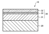
図1は、実施の形態1−1における位相シフトマスクブランク10の膜構成を示す模式図である。位相シフトマスクブランク10は、露光光に対して透明な透明基板20と、透明基板20上に配置された位相シフト膜30とを備える。透明基板20は、表面反射ロスが無いとしたときに、露光光に対して85%以上の透過率、好ましくは90%以上の透過率を有するものである。
FIG. 1 is a schematic view showing the film configuration of the phase shift mask blank 10 according to the first embodiment. The phase shift mask blank 10 includes a
位相シフト膜30は、1種以上の金属と、酸素、窒素、炭素から選ばれる少なくとも1つを含有する金属系材料、または、1種以上の金属と、ケイ素と、酸素、窒素、炭素から選ばれる少なくとも1つを含有する金属シリサイド系材料で構成される。
金属系材料に含有される金属としては、クロム(Cr)、Zr(ジルコニウム)、モリブデン(Mo)、タンタル(Ta)、タングステン(W)、チタン(Ti)などの遷移金属、アルミニウム(Al)などの典型金属が挙げられる。
金属シリサイド系材料としては、例えば、金属シリサイドの窒化物、金属シリサイドの酸化物、金属シリサイドの酸化窒化物、金属シリサイドの炭化窒化物、金属シリサイドの酸化炭化物、および、金属シリサイドの酸化炭化窒化物が挙げられる。金属シリサイド系材料に含有される金属としては、上述した遷移金属および典型金属が挙げられる。
The
Examples of the metal contained in the metal-based material include transition metals such as chromium (Cr), Zr (zirconium), molybdenum (Mo), tantalum (Ta), tungsten (W), and titanium (Ti), and aluminum (Al). Typical metal of.
Examples of the metal silicide-based material include metal nitride nitrides, metal silicide oxides, metal silicide oxidative nitrides, metal silicide carbide nitrides, metal silicide oxide carbides, and metal silicide oxide carbide nitrides. Can be mentioned. Examples of the metal contained in the metal silicide-based material include the above-mentioned transition metal and main group metal.
位相シフト膜30は、透明基板20側から、位相シフト層31と、中間層であるメタル層33と、反射率低減層32とを有している。
位相シフト膜30は、実施例において詳述するように、位相シフト層31と、反射率低減層32と、メタル層33の全てを金属系材料で構成してもよく(実施例1、2)、また、位相シフト層31と、反射率低減層32と、メタル層33のいずれか1層若しくは2層を金属系材料で構成して他の層を金属シリサイド系材料で構成してもよい(実施例3)。
The
As described in detail in Examples, the
位相シフト層31は、透明基板20の主表面上に配置される。位相シフト層31は、露光光に対する透過率と位相差とを主に調整する機能を有する。位相シフト層31は、位相シフト膜30において、反射率低減層32、メタル層33の膜厚と比べて一番膜厚の厚い層である。尚、後述する位相シフト層31、メタル層33、反射率低減層32を構成する各元素の含有率は、X線光電子分光法(XPS、ESCA)により測定された値とする。
位相シフト層31は、金属系材料または金属シリサイド系材料で構成される。
The
The
位相シフト膜30全体がクロム(Cr)系材料で構成される場合、位相シフト層31は、クロム(Cr)と酸素(O)と窒素(N)とを含有するクロム系材料で構成され、各元素の平均含有率は、クロムが30〜70原子%、酸素が20〜60原子%、窒素が0.4〜30原子%であることが好ましい。また、位相シフト層31は、該位相シフト層31を構成する成分の結合状態(化学状態)として、クロムと窒素が結合したクロム窒化物を含み、特に一窒化クロム(CrN)または窒化二クロム(Cr2N)を含むことが好ましい。さらに、位相シフト層31は、炭素(C)およびフッ素(F)のうちの少なくとも一種を含むクロム系材料を有してもよい。例えば、位相シフト層31を形成する材料として、CrON、CrOCN、CrFCONが挙げられる。
When the entire
また、位相シフト膜30を構成する金属シリサイド系材料の金属にモリブデン(Mo)やジルコニウム(Zr)やチタン(Ti)が含まれる場合、位相シフト層31は、モリブデン(Mo)と、ケイ素(Si)と、窒素(N)および/又は酸素(O)とを含有するモリブデンシリサイド系材料や、ジルコニウム(Zr)とケイ素(Si)と窒素(N)および/又は酸素(O)とを含有するジルコニウムシリサイド系材料や、チタン(Ti)とケイ素(Si)と窒素(N)および/又は酸素(O)とを含有するチタンシリサイド系材料で構成される。モリブデンシリサイド系材料の場合、各元素の平均含有率は、モリブデン(Mo)が5〜20原子%、ケイ素(Si)が15〜45原子%、窒素(N)が0〜75原子%、酸素(O)が0〜45原子%であることが好ましい。また、ジルコニウムシリサイド系材料の場合、各元素の平均含有率は、ジルコニウム(Zr)が5〜35原子%、ケイ素(Si)が5〜45原子%、窒素(N)が0〜70原子%、酸素(O)が0〜70原子%であることが好ましい。また、チタンシリサイド系材料の場合、各元素の平均含有率は、チタン(Ti)が5〜30原子%、ケイ素(Si)が10〜45原子%、窒素(N)が0〜70原子%、酸素(O)が0〜60原子%であることが好ましい。さらに、位相シフト層31は、炭素(C)を含むモリブデンシリサイド系材料や炭素(C)を含むジルコニウムシリサイド系材料を有してもよい。
位相シフト層31は、スパッタリング法により形成することができる。
When molybdenum (Mo), zirconium (Zr), or titanium (Ti) is contained in the metal of the metal silicide-based material constituting the
The
反射率低減層32は、位相シフト層31の上側に配置される。反射率低減層32は、位相シフト膜30側(すなわち、反射率低減層32の透明基板20側とは反対側)より入射される光に対する反射率を低減させる機能を主に有する。反射率低減層32は、メタル層33と反射率低減層32の界面による反射と反射率低減層32表面による反射による干渉効果により位相シフト膜30の反射率を低減するために膜厚調整されている層である。
反射率低減層32は、金属系材料または金属シリサイド系材料で構成される。
The
The
位相シフト膜30全体がクロム(Cr)系材料で構成される場合、反射率低減層32は、クロム(Cr)と酸素(O)と窒素(N)とを含有するクロム系材料で構成され、各元素の平均含有率は、クロムが30〜70原子%、酸素が20〜60原子%、窒素が0.4〜30原子%である。また、反射率低減層32は、該反射率低減層32を構成する成分の結合状態(化学状態)として、クロムと酸素が結合したクロム酸化物を含み、特に酸化クロム(III)(Cr2O3)を主に含むことが好ましい。さらに、反射率低減層32は、炭素(C)およびフッ素(F)のうちの少なくとも一種を含むクロム系材料を有してもよい。例えば、反射率低減層32を形成する材料として、CrON、CrOCN、CrFONが挙げられる。この場合、位相シフト膜側(反射率低減層32の表面側)より入射される光に対する反射率の低減効果と、位相シフト膜30全体として、ウェットエッチングにより優れたパターン断面形状を形成する観点から、位相シフト層31に含まれる窒素(N)の平均含有率は、反射率低減層32に含まれる窒素(N)の平均含有率と同じか、又はそれよりも多く、反射率低減層32に含まれる酸素(O)の平均含有率は、位相シフト層31に含まれる酸素(O)の平均含有率よりも多い状態とする。また、反射率低減層32に含まれる酸素(O)の平均含有率は、位相シフト層31に含まれる酸素(O)の平均含有率よりも少なくとも1原子%以上、好ましくは、5原子%以上多くすることが、膜面反射率の低減効果の点で好ましい。
When the entire
また、位相シフト膜30を構成する金属シリサイド系材料の金属にモリブデン(Mo)やジルコニウム(Zr)やチタン(Ti)が含まれる場合、反射率低減層32は、チタン(Ti)と窒素(N)と酸素(O)とを含有するチタン系材料や、チタン(Ti)と酸素(O)とを含有するチタン系材料で構成され、各元素の平均含有率は、チタン(Ti)が15〜45原子%、窒素(N)が20〜50原子%、酸素(O)が15〜65原子%であることが好ましい。また、位相シフト膜30を構成する金属シリサイド系材料の場合、反射率低減層32は、モリブデン(Mo)とケイ素(Si)と窒素(N)と酸素(O)とを含有するモリブデンシリサイド系材料、モリブデン(Mo)とケイ素(Si)と酸素(O)とを含有するモリブデンシリサイド系材料、ジルコニウム(Zr)とケイ素(Si)と窒素(N)と酸素(O)とを含有するジルコニウムシリサイド系材料、ジルコニウム(Zr)とケイ素(Si)と酸素(O)とを含有するジルコニウムシリサイド系材料、チタン(Ti)とケイ素(Si)と窒素(N)と酸素(O)とを含有するチタンシリサイド系材料、チタン(Ti)とケイ素(Si)と酸素(O)とを含有するチタンシリサイド系材料で構成されるようにしてもよいが、表面に形成されるレジスト膜(図示せず)との密着性を確保するために、HMDS(hexamethyldisilazane)等の表面処理を行うことが好ましい。
反射率低減層32は、スパッタリング法により形成することができる。
When molybdenum (Mo), zirconium (Zr), or titanium (Ti) is contained in the metal of the metal silicide-based material constituting the
The
メタル層33は、位相シフト層31と反射率低減層32との間に配置される。メタル層33は、露光光に対する透過率を調整する機能を有するとともに、反射率低減層32と組み合わさって、位相シフト膜30側より入射される光に対する反射率を低減させる機能を有する。さらに、位相シフト層と組み合わさって、透明基板20側より入射される光に対する反射率を低減させる機能を有する。
メタル層33は、反射率低減層32の金属の平均含有率よりも高い、金属の平均含有率を有する金属系材料であるか、または、反射率低減層32の金属とケイ素の合計の平均含有率よりも、高い合計の平均含有率を有する金属シリサイド系材料で構成される。
The
The
位相シフト膜30全体がクロム(Cr)系材料で構成される場合、または、位相シフト膜30を構成する金属シリサイド系材料の金属にモリブデン(Mo)、ジルコニウム(Zr)、チタン(Ti)が含まれる場合、メタル層33は、クロム(Cr)と炭素(C)とを含有し、各元素の平均含有率は、クロム(Cr)の含有率が55〜90原子%、炭素(C)の含有率が10〜45原子%であり、メタル層33に含まれるクロムの平均含有率は、位相シフト層31、反射率低減層32に含まれるクロムの平均含有率よりも多い。位相シフト膜30全体を同一のエッチャントでエッチングする場合、炭素(C)の平均含有率を10原子%以上とすることで、メタル層33の断面形状がテーパー形状となることを抑制することができる。また、メタル層33に含まれる炭素(C)の平均含有率を45原子%以下とすることで、メタル層33の断面形状がテーパー形状となることを抑制することができる。メタル層33に含まれる炭素(C)の平均含有率を上記適切な範囲とすることにより、適切なマスクプロセスでメタル層33にパターンを形成することができる。また、メタル層33は、窒素(N)、酸素(O)およびフッ素(F)のうちの少なくとも一種を含むクロム系材料をさらに有してもよい。例えば、メタル層33を形成する材料として、CrC、CrCN、CrCO、CrCF、CrCONが挙げられる。中でも、メタル層33は、クロム(Cr)と炭素(C)と酸素(O)とを含有したクロム系材料とすることが好ましい。そして、位相シフト層31、反射率低減層32、及びメタル層33を構成する成分の結合状態(化学状態)として、ウェットエッチングによる優れたパターン断面形状を得るという観点から、これら全ての層に酸化クロム(III)(Cr2O3)を含むことがさらに好ましい。
When the entire
また、位相シフト膜30を構成する金属系材料の金属にチタン(Ti)が含まれて金属シリサイド系材料の金属にモリブデン(Mo)や、ジルコニウム(Zr)や、チタン(Ti)が含まれる場合、メタル層33は、モリブデン(Mo)と、ケイ素(Si)と、炭素(C)及び/又は窒素(N)とを含有するモリブデンシリサイド系材料や、ジルコニウム(Zr)と、ケイ素(Si)と、炭素(C)及び/又は窒素(N)とを含有するジルコニウムシリサイド系材料や、チタン(Ti)とケイ素(Si)と、炭素(C)及び/又は窒素(N)とを含有するチタンシリサイド系材料で構成される。モリブデンシリサイド系材料の場合、各元素の平均含有率は、モリブデン(Mo)が5〜20原子%、ケイ素(Si)が15〜70原子%、炭素(C)が0〜20原子%、窒素(N)が0〜30原子%であることが好ましい。また、ジルコニウムシリサイド系材料の場合、各元素の平均含有率は、ジルコニウム(Zr)が5〜35原子%、ケイ素(Si)が5〜70原子%、炭素(C)が0〜20原子%、窒素(N)が0〜20原子%であることが好ましい。また、チタンシリサイド系材料の場合、各元素の平均含有率は、チタン(Ti)が5〜35原子%、ケイ素(Si)が5〜70原子%、炭素(C)が0〜20原子%、窒素(N)が0〜20原子%であることが好ましい。メタル層33に含まれるモリブデンシリサイドの平均含有率、ジルコニウムシリサイドの平均含有率、チタンシリサイドの平均含有率は、位相シフト層31、反射率低減層32に含まれるモリブデンシリサイドの平均含有率、ジルコニウムシリサイドの平均含有率、チタンシリサイドの平均含有率よりも多い。さらに、メタル層33は、炭素(C)、窒素(N)、および酸素(O)のうちの少なくとも一種を含むモリブデンシリサイド系材料やジルコニウムシリサイド系材料やチタンシリサイド系材料であってもよい。例えば、メタル層33を形成する材料として、MoSiC、MoSiN、MoSiCN、MoSiCO、MoSiCON、ZrSiC、ZrSiN、ZrSiCN、ZrSiCO、ZrSiCON、TiSiC、TiSiN、TiSiCN、TiSiCO、TiSiCONが挙げられる。
メタル層33を備えることにより、位相シフト膜30のシート抵抗が下がるため、位相シフトマスクブランクおよび位相シフトマスクのチャージアップを防止することができる。メタル層33を備えていない場合、位相シフトマスクブランクおよび位相シフトマスクをケースから出し入れするとき発生する電気が逃げずに位相シフトマスクブランクおよび位相シフトマスクに電気が貯まるため、異物を付着させやすい。また、位相シフトマスクに小さなパターンが形成されているとき、パターンからパターンに電気が飛び、静電気破壊が起こりやすい。
メタル層33は、スパッタリング法により形成することができる。
Further, when the metal of the metal-based material constituting the
By providing the
The
メタル層33は、350nm〜436nmの波長域において、反射率低減層32の消衰係数よりも高い消衰係数を有することが好ましい。また、313nm〜436nmの波長域において、反射率低減層32の消衰係数よりも高い消衰係数を有することが好ましい。
メタル層33の消衰係数と反射率低減層32の消衰係数との差は、好ましくは、1.5〜3.5であり、より好ましくは、1.8〜3.5である。消衰係数の差が、1.5〜3.5であると、メタル層33と反射率低減層32との界面の上記波長域(350nm〜436nmの波長域、または、313nm〜436nmの波長域)における反射率を高めることができるので、より反射率低減効果が発揮されるので好ましい。
なお、メタル層33は、350nm〜436nmの波長域において、位相シフト層31の消衰係数よりも高い消衰係数を有することが好ましい。また、313nm〜436nmの波長域において、位相シフト層31の消衰係数よりも高い消衰係数を有することが好ましい。
消衰係数は、n&kアナライザーやエリプソメータなどを用いて測定することができる。
The
The difference between the extinction coefficient of the
The
The extinction coefficient can be measured using an n & k analyzer, an ellipsometer, or the like.
メタル層33および反射率低減層32がクロム系材料で構成される場合、メタル層33は、反射率低減層32のクロム(Cr)平均含有率(原子%)よりも高いクロム(Cr)平均含有率(原子%)を有する。
メタル層33のCr平均含有率と反射率低減層32のCr平均含有率との差は、好ましくは、10〜80原子%であり、より好ましくは、15〜80原子%である。Cr平均含有率の差が、10〜80原子%であると、メタル層33と反射率低減層32との界面の上記波長域(350nm〜436nmの波長域、または、313nm〜436nmの波長域)における反射率を高めることができるので、より反射率低減効果が発揮されるので好ましい。なお、メタル層33のエッチング速度は、クロム(Cr)に窒素(N)、酸素(O)、炭素(C)、フッ素(F)を含有させてクロム系材料とすることにより調整することができる。例えば、クロム(Cr)に炭素(C)やフッ素(F)を含有させることにより、ウェットエッチング速度を遅くすることができ、クロム(Cr)に窒素(N)や酸素(O)を含有させることにより、ウェットエッチング速度を速くすることができる。メタル層33の上下に形成されている位相シフト層31、反射率低減層32とのウェットエッチング速度を考慮して、クロムに上述の元素を添加したクロム系材料とすることにより、エッチング後の位相シフト膜30の断面形状を良好にすることができる。
なお、メタル層33は、位相シフト層31のクロム(Cr)平均含有率よりも高いクロム(Cr)平均含有率を有している。
When the
The difference between the average Cr content of the
The
位相シフト層31、メタル層33および反射率低減層32の各々は、350nm〜436nmの波長域において、2.0以上の屈折率を有することが好ましい。2.0以上の屈折率を有すると、所望の光学特性(透過率および位相差)を得るために必要な位相シフト膜30の膜厚を薄膜化することができる。したがって、該位相シフト膜30を備えた位相シフトマスクブランク10を用いて作製される位相シフトマスクは、優れたパターン断面形状および優れたCD均一性を有する位相シフト膜パターンを備えることができる。
屈折率は、n&kアナライザーやエリプソメータなどを用いて測定することができる。
Each of the
The refractive index can be measured using an n & k analyzer, an ellipsometer, or the like.
位相シフト層31、メタル層33および反射率低減層32の積層構造により、露光光に対する位相シフト膜30の透過率および位相差は所定の光学特性を有する。
位相シフト膜30は、位相シフト層31、メタル層33および反射率低減層32のいずれの層も同一のエッチャントでエッチング可能な材料から構成されていてもよく、位相シフト層31、メタル層33および反射率低減層32のうち1または2つの層が、他の層とエッチング選択性を有する材料から構成されていてもよい。
Due to the laminated structure of the
The
露光光に対する位相シフト膜30の透過率は、位相シフト膜30として必要な値を満たす。位相シフト膜30の透過率は、露光光に含まれる所定の波長の光(以下、代表波長という)に対して、好ましくは、1%〜70%であり、より好ましくは、2%〜60%であり、さらに好ましくは3%〜50%である。すなわち、露光光が313nm以上436nm以下の波長範囲の光を含む複合光である場合、位相シフト膜30は、その波長範囲に含まれる代表波長の光に対して、上述した透過率を有する。例えば、露光光がj線(波長:313nm)、i線(波長:365nm)、h線(波長:405nm)およびg線(波長:436nm)を含む複合光である場合、位相シフト膜30は、j線、i線、h線およびg線のいずれかに対して、上述した透過率を有する。
The transmittance of the
露光光に対する位相シフト膜30の位相差は、位相シフト膜30として必要な値を満たす。位相シフト膜30の位相差は、露光光に含まれる代表波長の光に対して、好ましくは、160°〜200°であり、より好ましくは、170°〜190°である。この性質により、露光光に含まれる代表波長の光の位相を160°〜200°変えることができる。このため、位相シフト膜30を透過した代表波長の光と透明基板20のみを透過した代表波長の光との間に160〜200°の位相差が生じる。すなわち、露光光が313nm以上436nm以下の波長範囲の光を含む複合光である場合、位相シフト膜30は、その波長範囲に含まれる代表波長の光に対して、上述した位相差を有する。例えば、露光光がj線、i線、h線およびg線を含む複合光である場合、位相シフト膜30は、j線、i線、h線およびg線のいずれかに対して、上述した位相差を有する。
The phase difference of the
位相シフト膜30の透過率および位相差は、位相シフト膜30を構成する位相シフト層31、メタル層33および反射率低減層32の各々の組成および厚さを調整することにより制御することができる。このため、この実施の形態では、位相シフト膜30の透過率および位相差が上述した所定の光学特性を有するように、位相シフト層31、メタル層33および反射率低減層32の各々の組成および厚さが調整されている。なお、位相シフト膜30の透過率は、主に、位相シフト層31およびメタル層33の組成および厚さに影響される。位相シフト膜30の屈折率は、主に、位相シフト層31の組成および厚さに影響される。
透過率および位相差は、位相シフト量測定装置などを用いて測定することができる。
The transmittance and phase difference of the
The transmittance and the phase difference can be measured by using a phase shift amount measuring device or the like.
位相シフト膜30側より入射される光に対する位相シフト膜30の膜面反射率は、350nm〜436nmの波長域において15%以下である。また、313nm〜436nmの波長域において22.5%以下であることが好ましい。すなわち、位相シフト膜30側より入射される光に対する位相シフト膜30の膜面反射率は、350nm〜436nmの波長域において15%以下であり、波長域を313nm〜436nmに広げても、22%以下であることが好ましい。位相シフト膜30の膜面反射率が350nm〜436nmの波長域において15%以下であると、レーザー描画光に対する膜面反射率が低減するため、優れたCD均一性を有する位相シフトマスクを形成することができる。また、位相シフト膜30の膜面反射率が313nm〜436nmの波長域において22.5%以下であると、露光光に対する膜面反射率が低減するため、位相シフトマスクに形成されているパターンを転写する際に、表示装置基板からの反射光に起因する転写パターンのぼやけ(フレア)を防止することができる。位相シフト膜30の膜面反射率は、313nm〜436nmにおいて、好ましくは20%以下、さらに好ましくは15%以下が望ましい。
The film surface reflectance of the
位相シフト膜30の膜面反射率の変動幅は、好ましくは、350nm〜436nmの波長域において9%以下、さらに好ましくは、8.5%以下である。また、313nm〜436nmの波長域において12.5%以下であることが好ましく、さらに好ましくは、12%以下である。すなわち、位相シフト膜30の膜面反射率の変動幅は、350nm〜436nmの波長域において9%以下、さらには8.5%以下であることが好ましく、波長域を313nm〜436nmに広げても、12.5%以下、さらには12%以下であることが好ましい。
The fluctuation range of the film surface reflectance of the
透明基板20側より入射される光に対する位相シフト膜30の裏面反射率は、365nm〜436nmの波長域において20%以下である。また、313nm〜436nmの波長域においても20%以下であることが好ましい。位相シフト膜30の裏面反射率を上記範囲とすることで、位相シフト膜30の露光光に対する裏面反射率が低減するため、位相シフトマスクに形成されているパターンを転写する際に、露光機の光学系との反射光に起因する転写精度の悪化を抑制できる。位相シフト膜30の裏面反射率の要件に加えて、位相シフト膜30の膜面反射率が350nm〜436nmの波長域において20%以下であると、露光機の光学系との反射や、位相シフトマスクに貼り付けられるペリクルや表示装置基板との反射の影響を低減できるため、転写精度が良好となり、また表示装置基板に転写される転写パターンのCDエラーを防止する位相シフトマスクを形成することができる。
The back surface reflectance of the
位相シフト膜30の裏面反射率の変動幅は、好ましくは、365nm〜436nmの波長域において18%以下、さらに好ましくは、16%以下である。また、313nm〜436nmの波長域において18%以下であることが好ましく、さらに好ましくは、16%以下である。すなわち、位相シフト膜30の膜面反射率の変動幅は、350nm〜436nmの波長域において9%以下、さらには8.5%以下であることが好ましく、また、波長域を313nm〜436nmにおいて、12.5%以下、さらには12%以下であることが好ましい。
The fluctuation range of the back surface reflectance of the
位相シフト膜30の膜面反射率、裏面反射率およびそれらの変動幅は、位相シフト膜30を構成する位相シフト層31、メタル層33および反射率低減層32の各々の屈折率、消衰係数および厚さを調整することにより制御することができる。消衰係数および屈折率は、組成を調整することにより制御することができるため、この実施の形態では、位相シフト膜30の膜面反射率、裏面反射率およびそれらの変動幅が上述した所定の物性を有するように、位相シフト層31、メタル層33および反射率低減層32の各々の組成および厚さが調整されている。なお、位相シフト膜30の膜面反射率、裏面反射率およびそれらの変動幅は、主に、メタル層33および反射率低減層32の各々の組成および厚さに影響される。
膜面反射率および裏面反射率は、分光光度計などを用いて測定することができる。膜面反射率の変動幅は、350nm〜436nmまたは313nm〜436nmの波長域における最大の反射率と最小の反射率との差から求められる。
The film surface reflectance, back surface reflectance, and their fluctuation width of the
The film surface reflectance and the back surface reflectance can be measured using a spectrophotometer or the like. The fluctuation range of the film surface reflectance is determined from the difference between the maximum reflectance and the minimum reflectance in the wavelength range of 350 nm to 436 nm or 313 nm to 436 nm.
位相シフト層31は、組成の均一な単一の膜からなる場合であってもよいし、組成の異なる複数の膜からなる場合であってもよいし、厚さ方向に組成が連続的に変化する単一の膜からなる場合であってもよい。メタル層33および反射率低減層32についても同様である。
また、位相シフト層31とメタル層33の界面、メタル層33と反射率低減層32の界面に、各位相シフト層31、メタル層33、反射率低減層32を構成する各元素が連続的に組成傾斜した組成傾斜領域を有していても構わない。
The
Further, at the interface between the
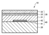
図2は、実施の形態1−2における位相シフトマスクブランク10の他の膜構成を示す模式図である。図2に示すように、位相シフトマスクブランク10は、透明基板20と位相シフト膜30との間に遮光性膜パターン40を備えるものであってもよい。実施の形態1−2における位相シフト膜30は、実施の形態1−1と同じであり説明は省略する。
FIG. 2 is a schematic view showing another film configuration of the phase shift mask blank 10 according to the first and second embodiments. As shown in FIG. 2, the phase shift mask blank 10 may include a light-shielding
位相シフトマスクブランク10が遮光性膜パターン40を備える場合、遮光性膜パターン40は、透明基板20の主表面上に配置される。遮光性膜パターン40は、露光光の透過を遮る機能を有する。
遮光性膜パターン40を形成する材料は、露光光の透過を遮る機能を有する材料であれば、特に制限されない。必要に応じて、遮光性膜パターン40の透明基板20側に、透明基板20側より入射される光に対する遮光性膜パターン40の裏面反射率を低減するための裏面反射率低減層41を形成しても構わない。この場合、遮光性膜パターン40は、透明基板20側から裏面反射率低減層41と、露光光の透過を遮る機能を有する遮光層42とを備えた構成となる。例えば、遮光性膜パターンの材料としては、クロム系材料などの金属系材料や、金属シリサイド系材料が挙げられる。クロム系材料として、クロム(Cr)、または、クロム(Cr)と、炭素(C)および窒素(N)のうちの少なくとも一種とを含むクロム系材料が挙げられる。その他、クロム(Cr)と、酸素(O)およびフッ素(F)のうちの少なくとも一種とを含むクロム系材料、または、クロム(Cr)と、炭素(C)および窒素(N)のうちの少なくとも一種とを含み、さらに、酸素(O)およびフッ素(F)のうちの少なくとも一種を含むクロム系材料が挙げられる。例えば、遮光性膜パターン40を形成する材料として、Cr、CrC、CrN、CrCN、CrO、CrON、CrCO、CrCONが挙げられる。
When the phase shift mask blank 10 includes the light-shielding
The material forming the light-shielding
金属シリサイド系材料としては、金属シリサイド、金属シリサイドの窒化物、金属シリサイドの酸化物、金属シリサイドの酸化窒化物、金属シリサイドの炭化窒化物、金属シリサイドの酸化炭化物、および金属シリサイドの酸化炭化窒化物が挙げられる。金属シリサイド系材料に含有される金属としては、上述した遷移金属および典型金属が挙げられる。
なお、遮光性膜パターン40が、裏面反射率低減層41を備える場合、裏面反射率低減層41は、365nm〜436nmの波長域において20%以下となる特性を有することが好ましい。さらに、裏面反射率低減層41は、313nm〜436nmの波長域において20%以下となる特性を有することが好ましい。
遮光性膜パターン40は、スパッタリング法により成膜した遮光性膜を、エッチングによりパターニングすることにより形成することができる。
Examples of metal silicide-based materials include metal silicides, metal besides nitride nitrides, metal silicide oxides, metal nitride oxide nitrides, metal silicide carbide nitrides, metal silicide oxide carbides, and metal silicide oxide carbide nitrides. Can be mentioned. Examples of the metal contained in the metal silicide-based material include the above-mentioned transition metal and main group metal.
When the light-shielding
The light-shielding
位相シフト膜30と遮光性膜パターン40とが積層する部分において、露光光に対する光学濃度は、好ましくは3以上であり、より好ましくは、3.5以上である。
光学濃度は、分光光度計もしくはODメーターなどを用いて測定することができる。
In the portion where the
The optical density can be measured using a spectrophotometer, an OD meter, or the like.
遮光性膜パターン40は、組成が均一な単一の膜からなる場合であってもよいし、組成が異なる複数の膜からなる場合であってもよいし、厚さ方向に組成が連続的に変化する単一の膜からなる場合であってもよい。
遮光性膜パターン40の材料は、位相シフト膜30(位相シフト層31、メタル層33、反射率低減層32)に対して、エッチング選択性を有する材料としてもよいし、エッチング選択性を有しない材料としてもよい。
The light-shielding
The material of the light-shielding
次に、図3は、実施の形態1−3における位相シフトマスクブランク10の他の膜構成を示す模式図である。図3に示すように、位相シフトマスクブランク10は、透明基板20と位相シフト膜30と遮光性膜45を備えるものであってもよい。遮光性膜45は、組成が均一な単一の膜からなる場合であってもよいし、組成が異なる複数の膜からなる場合であってもよいし、厚さ方向に組成が連続的に変化する単一の膜からなる場合であってもよい。実施の形態1−3における位相シフト膜30は、実施の形態1−1と同じであり説明は省略する。また、遮光性膜45を形成する材料は、露光光の透過を遮る機能を有する材料であれば、特に制限されない。必要に応じて、遮光性膜45の表面側に入射される光に対する遮光性膜45の膜面反射率を低減するための表面反射率低減層47を形成しても構わない。この場合、遮光性膜45は、位相シフト膜30側から露光光の透過を遮る機能を有する遮光層46と、表面反射率低減層47とを備えた構成となる。例えば、遮光性膜45の材料としては、上述の遮光性膜パターン40と同様の材料を使用することができる。なお、遮光性膜45が、表面反射率低減層47を備える場合、表面反射率低減層47は、365nm〜436nmの波長域において20%以下となる特性を有することが好ましい。また、さらに表面反射率低減層47は、313nm〜436nmの波長域において22.5%以下となる特性を有することが好ましい。なお、遮光層46および表面反射率低減層47は、それぞれ単一の層であってもよいし、または少なくともいずれかが複数の積層構造であってもよい。
遮光性膜45は、スパッタリング法により形成することができる。
Next, FIG. 3 is a schematic view showing another film configuration of the phase shift mask blank 10 in the first to third embodiments. As shown in FIG. 3, the phase shift mask blank 10 may include a
The light-shielding
実施の形態1−3において、遮光性膜45の材料は、位相シフト膜30(位相シフト層31、メタル層33、反射率低減層32)に対してエッチング選択性を有する材料としてもよいし、エッチング選択性を有しない材料としてもよい。位相シフトマスクの製造プロセスを考慮すると、遮光性膜45の材料は、位相シフト膜30に対してエッチング選択性を有する材料とすることが好ましい。
なお、実施の形態1−2や実施の形態1−3の位相シフトマスクブランク10において、必要に応じて、位相シフト膜30と遮光性膜パターン40との間、位相シフト膜30と遮光性膜45との間、遮光性膜45上に、他の機能膜を形成することもできる。前記機能膜としては、エッチング阻止膜やエッチングマスク膜などが挙げられる。
In the first to third embodiments, the material of the light-shielding
In addition, in the phase
なお、実施の形態1−1や実施の形態1−2の位相シフトマスクブランク10は、位相シフト膜30上にレジスト膜を備えるものであってもよいし、実施の形態1−3の位相シフトマスクブランク10は、遮光性膜45上にレジスト膜を備えるものであってもよい。
The phase
次に、上述の実施の形態1−1、1−2の位相シフトマスクブランク10の製造方法について説明する。位相シフトマスクブランク10は、以下の準備工程と位相シフト膜形成工程とを行うことによって製造される。
以下、各工程を詳細に説明する。
Next, a method for manufacturing the phase
Hereinafter, each step will be described in detail.
1.準備工程
準備工程では、先ず、透明基板20を準備する。透明基板20の材料は、使用する露光光に対して透光性を有する材料であれば、特に制限されない。例えば、合成石英ガラス、ソーダライムガラス、無アルカリガラスが挙げられる。
実施の形態1−2の遮光性膜パターン40を備える位相シフトマスクブランク10を製造する場合、その後、透明基板20上に、スパッタリング法により、例えば、クロム系材料からなる遮光性膜を形成する。その後、遮光性膜上にレジスト膜パターンを形成し、レジスト膜パターンをマスクにして遮光性膜をエッチングして、遮光性膜パターン40を形成する。その後、レジスト膜パターンを剥離する。なお、遮光性膜パターン40が、透明基板20側より入射される光に対する裏面反射率を低減する機能を有する場合、透明基板20上に、スパッタリング法により、例えば、クロムと酸素を含有する酸化クロムからなる裏面反射率低減層41と、裏面反射率低減層41上にクロムを含有するクロム系材料の遮光層42を形成して遮光性膜を形成する。その後、遮光性膜上にレジスト膜パターンを形成し、レジスト膜パターンをマスクにして遮光性膜をエッチングして、遮光性膜パターン40を形成する。その後、レジスト膜パターンを剥離して、透明基板20上に遮光性膜パターン40を得る。
1. 1. Preparation step In the preparation step, first, the
When the phase shift mask blank 10 having the light-shielding
2.位相シフト膜形成工程
位相シフト膜形成工程では、透明基板20上に、スパッタリング法により、金属系材料または金属シリサイド系材料からなる位相シフト膜30を形成する。ここで、透明基板20上に遮光性膜パターン40が形成されている場合、遮光性膜パターン40を覆うように、位相シフト膜30を形成する。
2. Phase shift film forming step In the phase shift film forming step, a
位相シフト膜30は、透明基板20の主表面上に位相シフト層31を成膜し、位相シフト層31上にメタル層33を成膜し、メタル層33上に反射率低減層32を成膜することにより形成される。以下においては、位相シフト膜30をクロム系材料で形成する場合について説明する。なお、位相シフト膜30を他の金属系材料または金属シリサイド系材料で形成する場合も、スパッタターゲットの材料とスパッタリング雰囲気を調整することで、同様にスパッタリング法で形成することができる。
The
位相シフト層31の成膜は、クロムまたはクロム系材料を含むスパッタターゲットを使用して、例えば、ヘリウムガス、ネオンガス、アルゴンガス、クリプトンガスおよびキセノンガスからなる群より選ばれる少なくとも一種を含む不活性ガスと、酸素ガス、窒素ガス、一酸化窒素ガス、二酸化窒素ガス、二酸化炭素ガス、炭化水素系ガス、フッ素系ガスからなる群より選ばれる少なくとも一種を含む活性ガスとの混合ガスからなるスパッタガス雰囲気で行われる。炭化水素系ガスとしては、例えば、メタンガス、ブタンガス、プロパンガス、スチレンガス等が挙げられる。スパッタターゲットとしては、クロム金属の他に、酸化クロム、窒化クロム、酸化窒化クロム、酸化窒化炭化クロム等のクロム系材料を使用することができる。
The film formation of the
同様に、メタル層33の成膜は、クロムまたはクロム系材料を含むスパッタターゲットを使用して、例えば、ヘリウムガス、ネオンガス、アルゴンガス、クリプトンガスおよびキセノンガスからなる群より選ばれる少なくとも一種を含む不活性ガスからなるスパッタガス雰囲気、または、ヘリウムガス、ネオンガス、アルゴンガス、クリプトンガスおよびキセノンガスからなる群より選ばれる少なくとも一種を含む不活性ガスと、酸素ガス、窒素ガス、一酸化窒素ガス、二酸化窒素ガス、二酸化炭素ガス、炭化水素系ガス、フッ素系ガスからなる群より選ばれる少なくとも一種を含む活性ガスとの混合ガスからなるスパッタガス雰囲気で行われる。炭化水素系ガスとしては、例えば、メタンガス、ブタンガス、プロパンガス、スチレンガス等が挙げられる。スパッタターゲットとしては、クロム金属の他に、酸化クロム、窒化クロム、酸化窒化クロム、酸化窒化炭化クロム等のクロム系材料を使用することができる。
Similarly, the formation of the
同様に、反射率低減層32の成膜は、クロムまたはクロム系材料を含むスパッタターゲットを使用して、例えば、ヘリウムガス、ネオンガス、アルゴンガス、クリプトンガスおよびキセノンガスからなる群より選ばれる少なくとも一種を含む不活性ガスと、酸素ガス、窒素ガス、一酸化窒素ガス、二酸化窒素ガス、二酸化炭素ガス、炭化水素系ガス、フッ素系ガスからなる群より選ばれる少なくとも一種を含む活性ガスとの混合ガスからなるスパッタガス雰囲気で行われる。炭化水素系ガスとしては、例えば、メタンガス、ブタンガス、プロパンガス、スチレンガス等が挙げられる。スパッタターゲットとしては、クロム金属の他に、酸化クロム、窒化クロム、酸化窒化クロム、酸化窒化炭化クロム等のクロム系材料を使用することができる。
Similarly, the film formation of the
位相シフト層31、メタル層33および反射率低減層32を成膜する際、位相シフト層31、メタル層33および反射率低減層32の各々の組成および厚さは、位相シフト膜30の透過率および位相差が上述した所定の光学特性を有し、かつ、位相シフト膜30の膜面反射率、裏面反射率およびそれらの変動幅が上述した所定の物性・光学特性を有するように調整される。位相シフト層31、メタル層33および反射率低減層32の各々の組成は、スパッタガスの組成および流量などにより制御することができる。位相シフト層31、メタル層33および反射率低減層32の各々の厚さは、スパッタパワー、スパッタリング時間などにより制御することができる。また、スパッタリング装置がインライン型スパッタリング装置の場合、基板の搬送速度によっても、位相シフト層31、メタル層33および反射率低減層32の各々の厚さを制御することができる。
When the
位相シフト層31が、組成の均一な単一の膜からなる場合、または複数の膜からなる場合、上述した成膜プロセスを、スパッタガスの組成および流量を変えずに1回だけ、または複数回行う。
位相シフト層31が、組成の異なる複数の膜からなる場合、上述した成膜プロセスを、成膜プロセス毎にスパッタガスの組成および流量を変えて複数回行う、スパッタターゲットの材料や組成を変えて複数回行う、又はそれらの組み合わせを複数回行う。
例えば、位相シフト層31が、厚さ方向に組成が連続的に変化する単一の膜からなる場合、上述した成膜プロセスを、スパッタガスの組成および流量を変化させながら1回だけ行う。メタル層33の成膜および反射率低減層32の成膜についても同様である。成膜プロセスを複数回行う場合、スパッタターゲットに印加するスパッタパワーを小さくすることができる。メタル層33および反射率低減層32の少なくともいずれかの組成が位相シフト層31と異なる場合にも、異なる組成がC,N,Oなどの非金属の組成であれば、上述した成膜プロセスを、成膜プロセス毎にスパッタガスの組成および流量を変えて行うことで、成膜することができる。なお、異なる組成が金属(Cr,Si,Zr)である場合には、ターゲットの変更が必要となる。この場合には、予め複数の組成の異なるターゲットを設置しておいて、目的の組成によって放電させるターゲットの位置を変更する。
When the
When the
For example, when the
位相シフト層31、メタル層33および反射率低減層32は、インライン型スパッタリング装置を用いて、透明基板20を装置外に取り出すことによって大気に曝すことなく、連続して成膜することが好ましい。装置外に取り出さずに、連続して成膜することにより、意図しない各層の表面酸化や表面炭化を防止することができる。各層の意図しない表面酸化や表面炭化は、位相シフト膜30上に形成されたレジスト膜を描画する際に使用するレーザー光や表示装置基板上に形成されたレジスト膜に位相シフト膜パターンを転写する際に使用する露光光に対する反射率を変化させたり、また、酸化部分や炭化部分のエッチングレートを変化させる恐れがある。
It is preferable that the
なお、レジスト膜を備える位相シフトマスクブランク10を製造する場合、次に、位相シフト膜上にレジスト膜を形成する。 When the phase shift mask blank 10 including the resist film is manufactured, the resist film is then formed on the phase shift film.
この実施の形態1−1の位相シフトマスクブランク10は、透明基板20上に設けられた金属系材料または金属シリサイド系材料からなる位相シフト膜30が、位相シフト層31と、反射率低減層32と、位相シフト層31と反射率低減層32との間に設けられた、反射率低減層32のクロム平均含有率よりも高い平均クロム含有率を有するメタル層33とを有しており、露光光に対する位相シフト膜30の透過率と位相差とが位相シフト膜30として必要な所定の光学特性を満たしつつ、位相シフト膜30の膜面反射率が、350nm〜436nmの波長域において15%以下であり、位相シフト膜30の裏面反射率が、365nm〜436nmの波長域において20%以下である。このため、この位相シフトマスクブランク10を用いて、優れたパターン断面形状および優れたCD均一性を有し、微細なパターンが形成されていて転写精度が良好となる位相シフトマスクを製造することができる。
In the phase
次に、実施の形態1−3における位相シフトマスクブランク10の製造方法について説明する。上述で説明した実施の形態1−3の位相シフトマスクブランク10の製造方法は、上述の「1.準備工程」、「2.位相シフト膜形成工程」は同じであるので説明は省略し、以下、遮光性膜形成工程について説明する。
Next, a method of manufacturing the phase shift mask blank 10 according to the first to third embodiments will be described. Since the method for manufacturing the phase
3.遮光性膜形成工程
遮光性膜形成工程では、位相シフト膜30上に、スパッタリング法により、金属系または金属シリサイド系材料からなる遮光性膜45を形成する。
遮光性膜45は、位相シフト膜30上に遮光層46、必要に応じて遮光層46上に表面反射率低減層47を成膜することにより形成される。以下においては、位相シフト膜30が金属シリサイド系材料とし、遮光性膜45をクロム系材料で形成する場合について説明する。なお、位相シフト膜30が金属系材料(例えば、クロム系材料)である場合に、遮光性膜45を金属シリサイド系材料で形成する場合や、位相シフト膜30と遮光性膜45が金属系材料(例えば、クロム系材料)である場合に、位相シフト膜30と遮光性膜45との間にエッチング選択性を有する材料(例えば、金属シリサイド系材料)で形成する場合も、スパッタリングターゲットの材料とスパッタリング雰囲気を調整することで、同様にスパッタリング法で形成することができる。
3. 3. Light-shielding film forming step In the light-shielding film forming step, a light-shielding
The light-shielding
遮光層46の成膜は、クロムまたはクロム系材料を含むスパッタターゲットを使用して、例えば、ヘリウムガス、ネオンガス、アルゴンガス、クリプトンガスおよびキセノンガスからなる群より選ばれる少なくとも一種を含む不活性ガスと、酸素ガス、窒素ガス、一酸化窒素ガス、二酸化窒素ガス、二酸化炭素ガス、炭化水素系ガス、フッ素系ガスからなる群より選ばれる少なくとも一種を含む活性ガスとの混合ガスからなるスパッタガス雰囲気で行われる。炭化水素系ガスとしては、例えば、メタンガス、ブタンガス、プロパンガス、スチレンガス等が挙げられる。スパッタターゲットとしては、クロム金属の他に、酸化クロム、窒化クロム、炭化クロム、酸化窒化クロム、酸化炭化クロム、窒化炭化クロム、酸化窒化炭化クロム等のクロム系材料を使用することができる。
The film formation of the light-
同様に、表面反射率低減層47の成膜は、クロムまたはクロム系材料を含むスパッタターゲットを使用して、例えば、ヘリウムガス、ネオンガス、アルゴンガス、クリプトンガスおよびキセノンガスからなる群より選ばれる少なくとも一種を含む不活性ガスと、酸素ガス、窒素ガス、一酸化窒素ガス、二酸化窒素ガス、二酸化炭素ガス、炭化水素系ガス、フッ素系ガスからなる群より選ばれる少なくとも一種を含む活性ガスとの混合ガスからなるスパッタガス雰囲気で行われる。炭化水素系ガスとしては、例えば、メタンガス、ブタンガス、プロパンガス、スチレンガス等が挙げられる。スパッタターゲットとしては、クロム金属の他に、酸化クロム、窒化クロム、炭化クロム、酸化窒化クロム、酸化炭化クロム、窒化炭化クロム、酸化窒化炭化クロム等のクロム系材料を使用することができる。
遮光層46、表面反射率低減層47を成膜する際、遮光層46および表面反射率低減層47の各々の組成および厚さは、遮光性膜45の光学濃度、膜面反射率が、上述した所定の物性・光学特性(位相シフト膜30と遮光性膜45との組み合わせにおいて、光学濃度が3.0以上で、遮光性膜45の膜面反射率が、350nm〜436nmの波長域において15%以下)を有するように調整される。遮光性膜45の遮光層46、表面反射率低減層47の各々の組成は、スパッタガスの組成および流量などにより制御することができる。遮光層46、表面反射率低減層47の各々の厚さは、スパッタパワー、スパッタリング時間などにより制御することができる。また、スパッタリング装置はインライン型スパッタリング装置の場合、基板の搬送速度によっても、遮光層46、表面反射率低減層47の各々の厚さを制御することができる。
Similarly, the film formation of the surface
When the light-
実施の形態2(実施の形態2−1、2−2).
実施の形態2では、位相シフトマスクの製造方法について説明する。実施の形態2−1は、実施の形態1−1、1−2の位相シフトマスクブランクを使用した位相シフトマスクの製造方法である。実施の形態2−2は、実施の形態1−3の位相シフトマスクブランクを使用した位相シフトマスクの製造方法である。実施の形態2−1の位相シフトマスクの製造方法は、実施の形態1−1、1−2の位相シフトマスクブランクを使用し、以下のレジスト膜パターンを形成する工程(レジスト膜パターン形成工程)と位相シフト膜パターンを形成する工程(位相シフト膜パターン形成工程)とを有し、実施の形態2−2の位相シフトマスクの製造方法は、実施の形態1−3の位相シフトマスクブランクを使用し、以下のレジスト膜パターン形成工程と、遮光性膜パターンを形成する工程(遮光性膜パターン形成工程)と、位相シフト膜パターン形成工程とを有する。
以下、各工程を詳細に説明する。
Embodiment 2 (Embodiments 2-1 and 2-2).
In the second embodiment, a method of manufacturing the phase shift mask will be described. Embodiment 2-1 is a method for manufacturing a phase shift mask using the phase shift mask blanks of Embodiments 1-1 and 1-2. Embodiment 2-2 is a method for manufacturing a phase shift mask using the phase shift mask blank of Embodiment 1-3. The method for manufacturing the phase shift mask of the second embodiment is a step of forming the following phase shift mask pattern using the phase shift mask blanks of the first and second embodiments (resist film pattern forming step). And a step of forming a phase shift film pattern (phase shift film pattern forming step), and the method of manufacturing the phase shift mask of the second embodiment uses the phase shift mask blank of the first to third embodiments. It also has the following resist film pattern forming step, a light-shielding film pattern forming step (light-shielding film pattern forming step), and a phase shift film pattern forming step.
Hereinafter, each step will be described in detail.
実施の形態2−1の位相シフトマスクの製造方法
1.レジスト膜パターン形成工程
レジスト膜パターン形成工程では、先ず、実施の形態1−1、1−2の位相シフトマスクブランク10の位相シフト膜30上に、レジスト膜を形成する。ただし、位相シフトマスクブランク10が、位相シフト膜30上にレジスト膜を備えるものである場合、レジスト膜の形成は行わない。使用するレジスト膜材料は、特に制限されない。後述する350nm〜436nmの波長域から選択されるいずれかの波長を有するレーザー光に対して感光するものであればよい。また、レジスト膜は、ポジ型、ネガ型のいずれであっても構わない。
その後、350nm〜436nmの波長域から選択されるいずれかの波長を有するレーザー光を用いて、レジスト膜に所定のパターンを描画する。レジスト膜に描画するパターンとして、ラインアンドスペースパターンやホールパターンが挙げられる。
その後、レジスト膜を所定の現像液で現像して、位相シフト膜30上にレジスト膜パターンを形成する。
Method for manufacturing a phase shift mask according to the first embodiment 1. Resist film pattern forming step In the resist film pattern forming step, first, a resist film is formed on the
Then, a predetermined pattern is drawn on the resist film using a laser beam having any wavelength selected from the wavelength range of 350 nm to 436 nm. Examples of the pattern drawn on the resist film include a line-and-space pattern and a hole pattern.
Then, the resist film is developed with a predetermined developer to form a resist film pattern on the
2.位相シフト膜パターン形成工程
位相シフト膜パターン形成工程では、先ず、レジスト膜パターンをマスクにして位相シフト膜30をエッチングして、位相シフト膜パターンを形成する。位相シフト膜30をエッチングするエッチング媒質(エッチング溶液、エッチングガス)は、位相シフト膜30を構成する位相シフト層31、メタル層33および反射率低減層32の各々をエッチングできるものであれば、特に制限されない。例えば、位相シフト膜30を構成する位相シフト層31、メタル層33および反射率低減層32の各々が、クロム(Cr)を含むクロム系材料から構成される場合、硝酸第二セリウムアンモニウムと過塩素酸とを含むエッチング溶液や、塩素ガスと酸素ガスの混合ガスからなるエッチングガスが挙げられる。また、位相シフト膜30を構成する位相シフト層31、メタル層33および反射率低減層32の各々が、金属シリサイド系材料から構成される場合、フッ化水素酸、珪フッ化水素酸、及びフッ化水素アンモニウムから選ばれた少なくとも一つのフッ素化合物と、過酸化水素、硝酸、及び硫酸から選ばれた少なくとも一つの酸化剤とを含むエッチング溶液や、過酸化水素とフッ化アンモニウムと、リン酸、硫酸、硝酸から選ばれた少なくとも一つの酸化剤とを含むエッチング溶液や、CF4ガス、CHF3ガス、SF6ガスなどのフッ素系ガスや、これらのガスにO2ガスを混合したエッチングガスが挙げられる。
その後、レジスト剥離液を用いて、または、アッシングによって、レジスト膜パターンを剥離する。
なお、位相シフト層31、メタル層33および反射率低減層32のうち1または2つの層が他の層とエッチング選択性を有する材料から構成されている場合、エッチング媒質を層に応じて変更することで、所望のエッチングを行うことができる。
2. Phase shift film pattern forming step In the phase shift film pattern forming step, first, the
Then, the resist film pattern is peeled off using a resist stripping solution or by ashing.
When one or two of the
この実施の形態2−1の位相シフトマスクの製造方法によれば、優れたパターン断面形状および優れたCD均一性を有し、微細なパターンが形成されていて転写精度が良好となる位相シフトマスクを製造することができる。 According to the method for manufacturing a phase shift mask according to the second embodiment, the phase shift mask has an excellent pattern cross-sectional shape and excellent CD uniformity, a fine pattern is formed, and the transfer accuracy is good. Can be manufactured.
実施の形態2−2の位相シフトマスクの製造方法
1.第1レジスト膜パターン形成工程
第1レジスト膜パターン形成工程では、先ず、実施の形態1−3の位相シフトマスクブランク10の遮光性膜45上に、レジスト膜を形成する。ただし、位相シフトマスクブランク10が、遮光性膜45上にレジスト膜を備えるものである場合、レジスト膜の形成は行わない。使用するレジスト膜材料は、特に制限されない。後述する350nm〜436nmの波長域から選択されるいずれかの波長を有するレーザー光に対して感光するものであればよい。また、レジスト膜は、ポジ型、ネガ型のいずれであっても構わない。
その後、350nm〜436nmの波長域から選択されるいずれかの波長を有するレーザー光を用いて、レジスト膜に所定のパターンを描画する。レジスト膜に描画するパターンとして、ラインアンドスペースパターンやホールパターンが挙げられる。
その後、レジスト膜を所定の現像液で現像して、遮光性膜45上に第1レジスト膜パターンを形成する。
Method for manufacturing a phase shift mask according to the second embodiment 1. First Resist Film Pattern Forming Step In the first resist film pattern forming step, first, a resist film is formed on the light-shielding
Then, a predetermined pattern is drawn on the resist film using a laser beam having any wavelength selected from the wavelength range of 350 nm to 436 nm. Examples of the pattern drawn on the resist film include a line-and-space pattern and a hole pattern.
Then, the resist film is developed with a predetermined developer to form a first resist film pattern on the light-shielding
2.位相シフト膜パターン形成用のマスクパターン形成工程(第1遮光性膜パターン形成工程)
マスクパターン形成工程は、第1レジスト膜パターンをマスクにして遮光性膜45をエッチングして、位相シフト膜パターン形成用のマスクパターンを形成する。遮光性膜45をエッチングするエッチング媒質(エッチング溶液、エッチングガス)は、遮光性膜45を構成する遮光層46、表面反射率低減層47の各々をエッチングできるものであれば、特に制限されない。例えば、遮光性膜45を構成する遮光層46、表面反射率低減層47の各々が、クロム(Cr)を含むクロム系材料から構成される場合、硝酸第二セリウムアンモニウムと過塩素酸とを含むエッチング溶液や、塩素ガスと酸素ガスの混合ガスからなるエッチングガスが挙げられる。また、遮光性膜45を構成する遮光層46、表面反射率低減層47の各々が、金属シリサイド系材料から構成される場合、フッ化水素酸、珪フッ化水素酸、及びフッ化水素アンモニウムから選ばれた少なくとも一つのフッ素化合物と、過酸化水素、硝酸、及び硫酸から選ばれた少なくとも一つの酸化剤とを含むエッチング溶液や、過酸化水素とフッ化アンモニウムと、リン酸、硫酸、硝酸から選ばれた少なくとも一つの酸化剤とを含むエッチング溶液や、CF4ガス、CHF3ガス、SF6ガスなどのフッ素系ガスや、これらのガスにO2ガスを混合したエッチングガスが挙げられる。
その後、レジスト剥離液を用いて、または、アッシングによって、レジスト膜パターンを剥離する。
2. Mask pattern forming step for phase shift film pattern forming (first light-shielding film pattern forming step)
In the mask pattern forming step, the light-shielding
Then, the resist film pattern is peeled off using a resist stripping solution or by ashing.
3.位相シフト膜パターン形成工程
位相シフト膜パターン形成工程は、上述のマスクパターン(第1遮光性膜パターン)をマスクにして位相シフト膜30をエッチングして、位相シフト膜パターンを形成する。位相シフト膜30をエッチングするエッチング媒質(エッチング溶液、エッチングガス)は、位相シフト膜30を構成する位相シフト層31、メタル層33および反射率低減層32の各々をエッチングできるものであれば、特に制限されない。エッチング媒質については、実施の形態2−1と同じであるので、説明は省略する。
3. 3. Phase shift film pattern forming step In the phase shift film pattern forming step, the
4.第2レジスト膜パターン形成工程
第2レジスト膜パターン形成工程は、位相シフト膜パターン上に所定の遮光性膜パターンを形成するためもので、第1遮光性膜パターン(上述のマスクパターン)上に第2レジスト膜パターンを形成する工程である。上述の工程で得られた位相シフト膜パターン、第1遮光性膜パターンを覆うようにレジスト膜を形成する。
その後、350nm〜436nmの波長域から選択されるいずれかの波長を有するレーザー光を用いて、レジスト膜に所定のパターンを描画する。レジスト膜に描画するパターンとして、ラインアンドスペースパターンやホールパターンが挙げられる。
その後、レジスト膜を所定の現像液で現像して、第1遮光性膜パターン上に第2レジスト膜パターンを形成する。
4. Second resist film pattern forming step The second resist film pattern forming step is for forming a predetermined light-shielding film pattern on the phase-shifted film pattern, and is on the first light-shielding film pattern (the above-mentioned mask pattern). 2 This is a step of forming a resist film pattern. A resist film is formed so as to cover the phase shift film pattern and the first light-shielding film pattern obtained in the above step.
Then, a predetermined pattern is drawn on the resist film using a laser beam having any wavelength selected from the wavelength range of 350 nm to 436 nm. Examples of the pattern drawn on the resist film include a line-and-space pattern and a hole pattern.
Then, the resist film is developed with a predetermined developer to form a second resist film pattern on the first light-shielding film pattern.
5.遮光性膜パターン形成工程
第2レジスト膜パターンをマスクにして第1遮光性膜パターンをエッチングして、位相シフト膜パターン上に遮光性膜パターンを形成する。第1遮光性膜パターンをエッチングするエッチング媒質(エッチング溶液、エッチングガス)は、上述で説明した遮光性膜45をエッチングするエッチング媒質と同じなので説明は省略する。
その後、レジスト剥離液を用いて、または、アッシングによって、第2レジスト膜パターンを剥離する。
この実施の形態2−2の位相シフトマスクの製造方法によれば、位相シフト膜パターン上に遮光性膜パターンが形成された位相シフトマスクであって、優れたパターン断面形状および優れたCD均一性を有し、微細なパターンが形成されていて転写精度が良好となる位相シフトマスクを製造することができる。
5. Light-shielding film pattern forming step The first light-shielding film pattern is etched by using the second resist film pattern as a mask to form a light-shielding film pattern on the phase shift film pattern. Since the etching medium (etching solution, etching gas) for etching the first light-shielding film pattern is the same as the etching medium for etching the light-shielding
Then, the second resist film pattern is peeled off using a resist stripping solution or by ashing.
According to the method for manufacturing a phase shift mask according to the second embodiment, the phase shift mask has a light-shielding film pattern formed on the phase shift film pattern, and has an excellent pattern cross-sectional shape and excellent CD uniformity. It is possible to manufacture a phase shift mask which has a fine pattern and has good transfer accuracy.
実施の形態3.
実施の形態3では、表示装置の製造方法について説明する。表示装置は、以下のマスク載置工程とパターン転写工程とを行うことによって製造される。
以下、各工程を詳細に説明する。
Embodiment 3.
In the third embodiment, a method of manufacturing the display device will be described. The display device is manufactured by performing the following mask mounting step and pattern transfer step.
Hereinafter, each step will be described in detail.
1.載置工程
載置工程では、実施の形態2−1、2−2で製造された位相シフトマスクを露光装置のマスクステージに載置する。ここで、位相シフトマスクは、露光装置の投影光学系を介して表示装置基板上に形成されたレジスト膜に対向するように配置される。
1. 1. Mounting step In the mounting step, the phase shift mask manufactured in Embodiments 2-1 and 2-2 is mounted on the mask stage of the exposure apparatus. Here, the phase shift mask is arranged so as to face the resist film formed on the display device substrate via the projection optical system of the exposure device.
2.パターン転写工程
パターン転写工程では、位相シフトマスクに露光光を照射して、表示装置基板上に形成されたレジスト膜に位相シフト膜パターンを転写する。露光光は、313nm〜436nmの波長域から選択される複数の波長の光を含む複合光や、313nm〜436nmの波長域からある波長域をフィルターなどでカットし選択された単色光である。例えば、露光光は、i線、h線およびg線を含む複合光や、j線、i線、h線およびg線を含む混合光や、i線の単色光である。露光光として複合光を用いると、露光光強度を高くしてスループットを上げることができるため、表示装置の製造コストを下げることができる。
さらに、位相シフト膜の裏面反射率が365〜436nmの波長域において20%以下となる位相シフトマスクであるため、露光装置側への反射の影響を抑えることができ、表示装置基板上に形成されたレジスト膜に対して高精度のパターン転写を行うことができる。また、位相シフト膜の膜面反射率が313nm〜436nmの波長域において22.5%以下となる位相シフトマスクにおいては、表示装置基板側からの反射光に起因する転写パターンのぼやけ(フレア)を防止することができ、さらに、表示装置基板上に形成されたレジスト膜に対して高精度のパターン転写を行うことができる。
上述の実施の形態1の位相シフトマスクブランク、及び実施の形態2の位相シフトマスクの製造方法により製造された位相シフトマスクは、等倍露光のプロジェクション露光用の位相シフトマスクブランク、及び位相シフトマスクで使用されるのが好ましい。特に、開口数(NA)が0.06〜0.15の等倍露光のプロジェクション露光の露光環境で使用されるのがよい。
2. Pattern transfer step In the pattern transfer step, the phase shift mask is irradiated with exposure light to transfer the phase shift film pattern to the resist film formed on the display device substrate. The exposure light is a composite light containing light having a plurality of wavelengths selected from the wavelength range of 313 nm to 436 nm, or monochromatic light selected by cutting a certain wavelength range from the wavelength range of 313 nm to 436 nm with a filter or the like. For example, the exposure light is a composite light including i-line, h-line and g-line, a mixed light including j-line, i-line, h-line and g-line, and i-line monochromatic light. When composite light is used as the exposure light, the exposure light intensity can be increased and the throughput can be increased, so that the manufacturing cost of the display device can be reduced.
Further, since the phase shift mask has a back surface reflectance of 20% or less in the wavelength range of 365 to 436 nm, the influence of reflection on the exposure device side can be suppressed, and the phase shift film is formed on the display device substrate. High-precision pattern transfer can be performed on the resist film. Further, in the phase shift mask in which the film surface reflectance of the phase shift film is 22.5% or less in the wavelength range of 313 nm to 436 nm, blurring (flare) of the transfer pattern due to the reflected light from the display device substrate side is caused. This can be prevented, and further, high-precision pattern transfer can be performed on the resist film formed on the display device substrate.
The phase shift mask manufactured by the above-described phase shift mask blank of the first embodiment and the phase shift mask manufacturing method of the second embodiment is a phase shift mask blank for projection exposure of the same magnification exposure and a phase shift mask. It is preferable to be used in. In particular, it is preferably used in an exposure environment of projection exposure with a numerical aperture (NA) of 0.06 to 0.15.
この実施の形態3の表示装置の製造方法によれば、CDエラーが生じない、高解像度、高精細の表示装置を製造することができる。 According to the method for manufacturing a display device according to the third embodiment, it is possible to manufacture a high-resolution, high-definition display device that does not cause a CD error.
以下、実施例および比較例に基づいて、本発明をより具体的に説明する。なお、以下の実施例は、本発明の一例であって、本発明を限定するものではない。 Hereinafter, the present invention will be described in more detail based on Examples and Comparative Examples. The following examples are examples of the present invention and do not limit the present invention.
実施例1〜5および比較例1の位相シフトマスクブランクは、透明基板と、透明基板上に配置された位相シフト膜とを備える。透明基板として、大きさが800mm×920mmであり、厚さが10mmである合成石英ガラス基板を用いた。
以下、実施例1〜5および比較例1について詳細に説明する。
The phase shift mask blanks of Examples 1 to 5 and Comparative Example 1 include a transparent substrate and a phase shift film arranged on the transparent substrate. As the transparent substrate, a synthetic quartz glass substrate having a size of 800 mm × 920 mm and a thickness of 10 mm was used.
Hereinafter, Examples 1 to 5 and Comparative Example 1 will be described in detail.
実施例1.
実施例1の位相シフトマスクブランクにおける位相シフト膜は、透明基板側から順に配置された、位相シフト層とメタル層と反射率低減層とから構成され、さらに、位相シフト層とメタル層の界面、メタル層と反射率低減層の界面に、組成傾斜領域が形成されている(図6参照)。
Example 1.
The phase shift film in the phase shift mask blank of Example 1 is composed of a phase shift layer, a metal layer, and a reflectance reduction layer arranged in order from the transparent substrate side, and further, an interface between the phase shift layer and the metal layer. A composition gradient region is formed at the interface between the metal layer and the reflectance reduction layer (see FIG. 6).
実施例1の位相シフトマスクブランクは、以下の方法により製造した。
先ず、透明基板である合成石英ガラス基板を準備した。透明基板の両主表面は鏡面研磨されている。実施例2〜5および比較例1において準備した透明基板の両主表面も同様に鏡面研磨されている。
次に、透明基板をインライン型スパッタリング装置に搬入した。インライン型スパッタリング装置には、スパッタ室が設けられている。
次に、スパッタ室に配置されたクロムターゲットに2.7kWのスパッタパワーを印加し、ArガスとN2ガスとCO2ガスとO2ガスとの混合ガスをスパッタ室内に導入しながら、200mm/分の速度で透明基板を搬送させた。ここで、混合ガスは、Arが35sccm、N2が35sccm、CO2が13sccm、O2が10sccmの流量となるようにスパッタ室内に導入した。透明基板がクロムターゲット付近を通過する際に、透明基板上にCrとCとOとNを含むクロム系材料(CrCON)からなる位相シフト層を成膜した。
The phase shift mask blank of Example 1 was manufactured by the following method.
First, a synthetic quartz glass substrate, which is a transparent substrate, was prepared. Both main surfaces of the transparent substrate are mirror-polished. Both main surfaces of the transparent substrates prepared in Examples 2 to 5 and Comparative Example 1 are also mirror-polished in the same manner.
Next, the transparent substrate was carried into the in-line sputtering apparatus. The in-line sputtering apparatus is provided with a sputtering chamber.
Next, 2.7 kW of sputtering power was applied to the chromium target placed in the sputtering chamber, and 200 mm / mm / while introducing a mixed gas of Ar gas, N 2 gas, CO 2 gas and O 2 gas into the sputtering chamber. The transparent substrate was conveyed at a speed of 1 minute. Here, the mixed gas was introduced into the sputtering chamber so that Ar had a flow rate of 35 sccm, N 2 had a flow rate of 35 sccm, CO 2 had a flow rate of 13 sccm, and O 2 had a flow rate of 10 sccm. When the transparent substrate passed near the chromium target, a phase shift layer made of a chromium-based material (CrCON) containing Cr, C, O, and N was formed on the transparent substrate.
次に、クロムターゲットに0.6kWのスパッタパワーを印加し、ArガスとCH4ガスとの混合ガス(Arガス中に4%の濃度でCH4ガスが含まれている混合ガスをスパッタ室内に導入しながら、400mm/分の速度で透明基板を搬送させた。透明基板がクロムターゲット付近を通過する際に、位相シフト層上にCrとCを含むクロム系材料(CrC)からなるメタル層を成膜した。
次に、クロムターゲットに3.3kWのスパッタパワーを印加し、ArガスとN2ガスとCO2ガスとO2ガスとの混合ガスをスパッタ室内に導入しながら、400mm/分の速度で透明基板を搬送させた。透明基板がクロムターゲット付近を通過する際に、メタル層上にCrとCとOとNを含むクロム系材料(CrCON)からなる反射率低減層を成膜した。ここで、混合ガスは、Arが35sccm、N2が35sccm、CO2が13sccm、O2が9sccmの流量となるようにスパッタ室内に導入した。
次に、位相シフト層とメタル層と反射率低減層とから構成される位相シフト膜が形成された透明基板をインライン型スパッタリング装置から取り出し、洗浄を行った。
なお、位相シフト層の成膜、メタル層の成膜、および反射率低減層の成膜は、透明基板をインライン型スパッタリング装置外に取り出すことによって大気に曝すことなく、インライン型スパッタリング装置内で連続して行った。
Next, a sputter power of 0.6 kW was applied to the chromium target, and a mixed gas of Ar gas and CH 4 gas (a mixed gas containing CH 4 gas at a concentration of 4% in Ar gas was introduced into the sputter chamber. While introducing, the transparent substrate was conveyed at a speed of 400 mm / min. When the transparent substrate passed near the chromium target, a metal layer made of a chromium-based material (CrC) containing Cr and C was formed on the phase shift layer. A film was formed.
Next, while applying a sputtering power of 3.3 kW to the chromium target and introducing a mixed gas of Ar gas, N 2 gas, CO 2 gas and O 2 gas into the sputtering chamber, a transparent substrate was introduced at a speed of 400 mm / min. Was transported. When the transparent substrate passed near the chromium target, a reflectance reducing layer made of a chromium-based material (CrCON) containing Cr, C, O, and N was formed on the metal layer. Here, the mixed gas was introduced into the sputtering chamber so that Ar had a flow rate of 35 sccm, N 2 had a flow rate of 35 sccm, CO 2 had a flow rate of 13 sccm, and O 2 had a flow rate of 9 sccm.
Next, the transparent substrate on which the phase shift film composed of the phase shift layer, the metal layer, and the reflectance reduction layer was formed was taken out from the in-line sputtering apparatus and washed.
The phase shift layer, the metal layer, and the reflectance reduction layer are continuously formed in the in-line sputtering apparatus without being exposed to the atmosphere by taking the transparent substrate out of the in-line sputtering apparatus. I went.
実施例1の位相シフト層、メタル層、反射率低減層より構成される位相シフト膜は、インライン型スパッタリング装置で成膜しているので、位相シフト層とメタル層との界面、メタル層と反射率低減層との界面に、各層を構成する元素が連続的に組成傾斜している組成傾斜領域が形成されている。
実施例1の位相シフト膜について、深さ方向の組成をX線光電子分光法(ESCA)により測定した結果を、図6に示す。
位相シフト層は、クロム(Cr)と酸素(O)と窒素(N)と炭素(C)とを含むクロム系材料で構成されており、各元素の平均含有率は、Cr:49.8原子%、O:40.0原子%、N:8.2原子%、C:2.0原子%あった。また、メタル層は、クロム(Cr)と炭素(C)と酸素(O)とを含むクロム系材料で構成されており、各元素の平均含有率は、Cr:69.9原子%、C:22.7原子%、O:7.4原子%であった。さらに、反射率低減層は、クロム(Cr)と酸素(O)と窒素(N)と炭素(C)とを含むクロム系材料で構成されており、各元素の平均含有率は、Cr:48.5原子%、O:47.4原子%、N:3.7原子%、C:0.4原子%あった。また、位相シフト層とメタル層との間、メタル層と反射率低減層との間には、連続的に各元素が減少又は増加した組成傾斜領域を有していた。
Since the phase shift film composed of the phase shift layer, the metal layer, and the reflectance reduction layer of Example 1 is formed by an in-line sputtering apparatus, the interface between the phase shift layer and the metal layer, the metal layer and the reflection At the interface with the rate reduction layer, a composition gradient region in which the elements constituting each layer are continuously gradient in composition is formed.
The results of measuring the composition of the phase shift film of Example 1 in the depth direction by X-ray photoelectron spectroscopy (ESCA) are shown in FIG.
The phase shift layer is composed of a chromium-based material containing chromium (Cr), oxygen (O), nitrogen (N), and carbon (C), and the average content of each element is Cr: 49.8 atoms. %, O: 40.0 atomic%, N: 8.2 atomic%, C: 2.0 atomic%. The metal layer is composed of a chromium-based material containing chromium (Cr), carbon (C), and oxygen (O), and the average content of each element is Cr: 69.9 atomic%, C: It was 22.7 atomic% and O: 7.4 atomic%. Further, the reflectance reducing layer is composed of a chromium-based material containing chromium (Cr), oxygen (O), nitrogen (N) and carbon (C), and the average content of each element is Cr: 48. There were 5.5 atomic%, O: 47.4 atomic%, N: 3.7 atomic%, and C: 0.4 atomic%. Further, between the phase shift layer and the metal layer, and between the metal layer and the reflectance reducing layer, there was a composition gradient region in which each element was continuously decreased or increased.
また、各層のCr、O、Nのスペクトルから、元素の結合状態(化学状態)を評価した。その結果、位相シフト層は、主として一窒化クロム(CrN)を含み、さらに酸化クロム(III)(Cr2O3)が存在していることが確認できた。
また、メタル層を構成する元素の結合状態(化学状態)は、主としてクロム(Cr)を含み、さらに酸化クロム(III)(Cr2O3)が存在していることが確認できた。
また、反射率低減層を構成する元素の結合状態(化学状態)は、主として酸化クロム(III)(Cr2O3)を含み、一窒化クロム(CrN)と窒化二クロム(Cr2N)が存在していることが確認できた。
In addition, the bonding state (chemical state) of the elements was evaluated from the spectra of Cr, O, and N of each layer. As a result, it was confirmed that the phase shift layer mainly contained chromium mononitride (CrN) and further contained chromium (III) oxide (Cr 2 O 3).
Further, it was confirmed that the bonding state (chemical state) of the elements constituting the metal layer mainly contained chromium (Cr), and that chromium (III) oxide (Cr 2 O 3 ) was further present.
The bonding state (chemical state) of the elements constituting the reflectance reduction layer mainly contains chromium (III) oxide (Cr 2 O 3 ), and chromium mononitride (Cr N) and dichromium nitride (Cr 2 N). It was confirmed that it exists.
位相シフト膜は、上述した3層構造により、365nmの光に対する透過率は4.9%および位相差は187°を有していた。
なお、透過率および位相差は、レーザーテック社製のMPM−100(商品名)を用いて測定した。実施例2〜5および比較例1においても同様に測定した。
The phase shift film had a transmittance of 4.9% and a phase difference of 187 ° with respect to light at 365 nm due to the above-mentioned three-layer structure.
The transmittance and the phase difference were measured using MPM-100 (trade name) manufactured by Lasertec. The measurement was carried out in the same manner in Examples 2 to 5 and Comparative Example 1.
図4中の曲線aは、実施例1の位相シフトマスクブランクの位相シフト膜の膜面反射率スペクトルを示す。図5中の曲線aは、実施例1の位相シフトマスクブランクの位相シフト膜の裏面反射率スペクトルを示す。
図4に見られるように、位相シフト膜は、膜面反射率が、313nmの波長において13.3%であり、350nmにおいて9.6%であり、365nmの波長において8.3%であり、405nmの波長において7.1%であり、413nm波長において7.3%であり、436nmの波長において8.1%であった。また、位相シフト膜は、膜面反射率の変動幅が、350nm〜436nmの波長域において、2.5%であり、365nm〜436nmの波長域において、1.2%であり、313nm〜436nmの波長域において、6.2%であった。
The curve a in FIG. 4 shows the film surface reflectance spectrum of the phase shift film of the phase shift mask blank of Example 1. The curve a in FIG. 5 shows the back surface reflectance spectrum of the phase shift film of the phase shift mask blank of Example 1.
As can be seen in FIG. 4, the phase shift film has a film surface reflectance of 13.3% at a wavelength of 313 nm, 9.6% at 350 nm, and 8.3% at a wavelength of 365 nm. It was 7.1% at the wavelength of 405 nm, 7.3% at the wavelength of 413 nm, and 8.1% at the wavelength of 436 nm. Further, in the phase shift film, the fluctuation range of the film surface reflectance is 2.5% in the wavelength range of 350 nm to 436 nm, 1.2% in the wavelength range of 365 nm to 436 nm, and 313 nm to 436 nm. In the wavelength range, it was 6.2%.
図5に見られるように、位相シフト膜は、裏面反射率が、313nmの波長において9.7%であり、350nmにおいて8.8%であり、365nmの波長において9.0%であり、405nmの波長において12.3%であり、413nm波長において13.2%であり、436nmの波長において16.1%であった。また、位相シフト膜は、膜面反射率の変動幅が、350nm〜436nmの波長域において、7.3%であり、365nm〜436nmの波長域において、7.1%であり、313nm〜436nmの波長域において、7.3%であった。
このように、位相シフト膜の膜面反射率が350nm〜436nmの波長域において15%以下となっており、さらに、位相シフト膜の裏面反射率が、365nm〜436nmの波長域において20%以下となっているので、この位相シフトマスクブランクを用いて、優れたパターン断面形状および優れたCD均一性を有し、微細なパターンが形成されていて転写精度が良好となる位相シフトマスクを製造することができる。
なお、膜面反射率および裏面反射率は、島津製作所社製のSolidSpec−3700(商品名)を用いて測定した。実施例2〜5および比較例1においても同様に測定した。
As can be seen in FIG. 5, the backside reflectance of the phase shift film is 9.7% at a wavelength of 313 nm, 8.8% at 350 nm, 9.0% at a wavelength of 365 nm, and 405 nm. It was 12.3% at the wavelength of 413 nm, 13.2% at the wavelength of 413 nm, and 16.1% at the wavelength of 436 nm. Further, in the phase shift film, the fluctuation range of the film surface reflectance is 7.3% in the wavelength range of 350 nm to 436 nm, 7.1% in the wavelength range of 365 nm to 436 nm, and 313 nm to 436 nm. In the wavelength range, it was 7.3%.
As described above, the surface reflectance of the phase shift film is 15% or less in the wavelength range of 350 nm to 436 nm, and the back surface reflectance of the phase shift film is 20% or less in the wavelength range of 365 nm to 436 nm. Therefore, using this phase shift mask blank, it is possible to manufacture a phase shift mask having an excellent pattern cross-sectional shape and excellent CD uniformity, in which a fine pattern is formed and the transfer accuracy is good. Can be done.
The film surface reflectance and the back surface reflectance were measured using SolidSpec-3700 (trade name) manufactured by Shimadzu Corporation. The measurement was carried out in the same manner in Examples 2 to 5 and Comparative Example 1.
上述した位相シフトマスクブランクを用いて、以下の方法により位相シフトマスクを製造した。
先ず、上述した位相シフトマスクブランクの位相シフト膜上に、ノボラック系のポジ型のフォトレジストからなるレジスト膜を形成した。
その後、レーザー描画機により、波長413nmのレーザー光を用いて、レジスト膜に所定のパターンを描画した。
その後、レジスト膜を所定の現像液で現像して、位相シフト膜上にレジスト膜パターンを形成した。
Using the above-mentioned phase shift mask blank, a phase shift mask was manufactured by the following method.
First, a resist film made of a novolac-based positive photoresist film was formed on the phase shift film of the above-mentioned phase shift mask blank.
Then, a predetermined pattern was drawn on the resist film by a laser drawing machine using a laser beam having a wavelength of 413 nm.
Then, the resist film was developed with a predetermined developer to form a resist film pattern on the phase shift film.
その後、レジスト膜パターンをマスクにして位相シフト膜をエッチングして、位相シフト膜パターンを形成した。位相シフト膜を構成する位相シフト層、メタル層および反射率低減層の各々は、クロム(Cr)を含むクロム系材料から形成される。このため、位相シフト層、メタル層および反射率低減層は、同じエッチング溶液によりエッチングすることができる。ここでは、位相シフト膜をエッチングするエッチング溶液として、硝酸第二セリウムアンモニウムと過塩素酸とを含むエッチング溶液を用いた。
その後、レジスト剥離液を用いて、レジスト膜パターンを剥離した。
Then, the phase shift film was etched by using the resist film pattern as a mask to form the phase shift film pattern. Each of the phase shift layer, the metal layer and the reflectance reducing layer constituting the phase shift film is formed of a chromium-based material containing chromium (Cr). Therefore, the phase shift layer, the metal layer, and the reflectance reducing layer can be etched with the same etching solution. Here, as an etching solution for etching the phase shift film, an etching solution containing dicerium ammonium nitrate and perchloric acid was used.
Then, the resist film pattern was peeled off using a resist stripping solution.
上述した位相シフトマスクブランクを用いて製造された位相シフトマスクの位相シフト膜パターン断面は、位相シフト膜パターンの膜厚方向の中央部に位置するメタル層において若干の食われが発生しているが、マスク特性に影響ない程度のものであった。
なお、位相シフトマスクの位相シフト膜パターン断面は、電子顕微鏡(日本電子株式会社製のJSM7401F(商品名))を用いて観察した。実施例2〜3および比較例1においても同様に測定した。
In the phase shift film pattern cross section of the phase shift mask manufactured by using the above-mentioned phase shift mask blank, the metal layer located at the center of the phase shift film pattern in the film thickness direction is slightly eaten. , It did not affect the mask characteristics.
The phase shift film pattern cross section of the phase shift mask was observed using an electron microscope (JSM7401F (trade name) manufactured by JEOL Ltd.). The measurement was carried out in the same manner in Examples 2 to 3 and Comparative Example 1.
上述した位相シフトマスクブランクを用いて製造された位相シフトマスクの位相シフト膜パターンのCDばらつき(CD均一性)は、70nmであり、良好であった。CDばらつき(CD均一性)は、目標とするラインアンドスペースパターン(ラインパターンの幅:2.0μm、スペースパターンの幅:2.0μm)からのずれ幅である。
なお、位相シフトマスクの位相シフト膜パターンのCDばらつきは、セイコーインスツルメンツナノテクノロジー社製SIR8000を用いて測定した。実施例2〜5および比較例1においても同様に測定した。
The CD variation (CD uniformity) of the phase shift film pattern of the phase shift mask manufactured by using the above-mentioned phase shift mask blank was 70 nm, which was good. The CD variation (CD uniformity) is the deviation width from the target line-and-space pattern (line pattern width: 2.0 μm, space pattern width: 2.0 μm).
The CD variation of the phase shift film pattern of the phase shift mask was measured using SIR8000 manufactured by Seiko Instruments Nanotechnology. The measurement was carried out in the same manner in Examples 2 to 5 and Comparative Example 1.
上述した位相シフトマスクは、優れたパターン断面形状および優れたCD均一性、良好な転写精度を有し、また、露光光に対する位相シフト膜パターンの膜面反射率および裏面反射率が低く、位相シフト膜パターンの裏面反射率も低いため、上述した位相シフトマスクを用いて、表示装置を製造したところ、CDエラーが生じない、高解像度、高精細の表示装置を製造することができた。なお、表示装置の製造工程における位相シフトマスクを使用したパターン転写工程は、開口数(NA)が0.1の等倍露光のプロジェクション露光であって、露光光はj線、i線、h線およびg線を含む複合光とした。 The above-mentioned phase shift mask has excellent pattern cross-sectional shape, excellent CD uniformity, and good transfer accuracy, and also has low film surface reflectance and back surface reflectance of the phase shift film pattern with respect to exposure light, so that the phase shift mask is used. Since the back surface reflectance of the film pattern is also low, when a display device was manufactured using the above-mentioned phase shift mask, it was possible to manufacture a high-resolution, high-definition display device that does not cause a CD error. The pattern transfer step using the phase shift mask in the manufacturing process of the display device is a projection exposure of 1x exposure with a numerical aperture (NA) of 0.1, and the exposure light is j-line, i-line, h-line. And a composite light containing g-line.
実施例2.
実施例2の位相シフトマスクブランクにおける位相シフト膜は、透明基板側から順に配置された、位相シフト層とメタル層と反射率低減層とから構成される。
実施例2の位相シフトマスクブランクにおける位相シフト層、メタル層、反射率低減層の各層は、以下の成膜条件により成膜した。
位相シフト層は、混合ガスとして、Arが35sccm、N2が35sccm、CO2が100sccm、O2が35sccmの流量となるようにスパッタ室内に導入した以外は、実施例1と同様にして透明基板上にCrとOとNを含むクロム系材料(CrON)からなる位相シフト層を成膜した。
次に、メタル層は、スパッタ室に配置されたクロムターゲットに0.5kWのスパッタパワーを印加した以外は実施例1と同様にして位相シフト層上にCrとCを含むクロム系材料(CrC)からなるメタル層を成膜した。
次に、反射率低減層は、混合ガスとして、Arが35sccm、N2が35sccm、CO2が100sccm、O2が35sccmの流量となるようにスパッタ室内に導入した以外は、実施例1と同様にしてメタル層上にCrとOとNを含むクロム系材料(CrON)からなる反射率低減層を成膜した。
Example 2.
The phase shift film in the phase shift mask blank of the second embodiment is composed of a phase shift layer, a metal layer, and a reflectance reducing layer arranged in order from the transparent substrate side.
Each of the phase shift layer, the metal layer, and the reflectance reduction layer in the phase shift mask blank of Example 2 was formed under the following film forming conditions.
The phase shift layer is a transparent substrate in the same manner as in Example 1 except that the phase shift layer is introduced into the sputter chamber as a mixed gas so that Ar is 35 sccm, N 2 is 35 sccm, CO 2 is 100 sccm, and O 2 is 35 sccm. A phase shift layer made of a chromium-based material (CrON) containing Cr, O, and N was formed on the film.
Next, the metal layer is a chromium-based material (CrC) containing Cr and C on the phase shift layer in the same manner as in Example 1 except that a sputtering power of 0.5 kW is applied to the chromium target arranged in the sputtering chamber. A metal layer made of the above was formed.
Next, the reflectance reducing layer is the same as in Example 1 except that the mixed gas is introduced into the sputtering chamber so that Ar has a flow rate of 35 sccm, N 2 has a flow rate of 35 sccm, CO 2 has a flow rate of 100 sccm, and O 2 has a flow rate of 35 sccm. Then, a reflectance reducing layer made of a chromium-based material (CrON) containing Cr, O, and N was formed on the metal layer.
実施例2の位相シフト膜について、深さ方向の組成をX線光電子分光法(ESCA)により測定した結果、位相シフト層は、主にクロム(Cr)と酸素(O)と窒素(N)とを含むクロム系材料で構成されており、各元素の平均含有率は、Cr:45.5原子%、O:53.8原子%、N:0.6原子%、C:0.1原子%あった。また、メタル層は、クロム(Cr)と炭素(C)と酸素(O)とを含むクロム系材料で構成されており、各元素の平均含有率は、Cr:74.7原子%、C:15.8原子%、O:8.8原子%、N:0.7原子%であった。さらに、反射率低減層は、主にクロム(Cr)と酸素(O)と窒素(N)とを含むクロム系材料で構成されており、各元素の平均含有率は、Cr:44.4原子%、O:55.0原子%、N:0.5原子%、C:0.1原子%あった。また、位相シフト層とメタル層との間、メタル層と反射率低減層との間には、連続的に各元素が減少又は増加した組成傾斜領域を有していた。 As a result of measuring the composition in the depth direction of the phase shift film of Example 2 by X-ray photoelectron spectroscopy (ESCA), the phase shift layer mainly contains chromium (Cr), oxygen (O) and nitrogen (N). It is composed of a chromium-based material containing, and the average content of each element is Cr: 45.5 atomic%, O: 53.8 atomic%, N: 0.6 atomic%, C: 0.1 atomic%. there were. The metal layer is composed of a chromium-based material containing chromium (Cr), carbon (C), and oxygen (O), and the average content of each element is Cr: 74.7 atomic%, C :. It was 15.8 atomic%, O: 8.8 atomic%, and N: 0.7 atomic%. Further, the reflectance reducing layer is mainly composed of a chromium-based material containing chromium (Cr), oxygen (O) and nitrogen (N), and the average content of each element is Cr: 44.4 atoms. %, O: 55.0 atomic%, N: 0.5 atomic%, C: 0.1 atomic%. Further, between the phase shift layer and the metal layer, and between the metal layer and the reflectance reducing layer, there was a composition gradient region in which each element was continuously decreased or increased.
また、各層のCr、O、Nのスペクトルから、元素の結合状態(化学状態)を評価した。その結果、位相シフト層は、主として窒化二クロム(Cr2N)を含み、さらに酸化クロム(III)(Cr2O3)と酸化クロム(VI)(CrO3)が存在していることが確認できた。
また、メタル層を構成する元素の結合状態(化学状態)は、主としてクロム(Cr)を含み、さらに酸化クロム(III)(Cr2O3)が存在していることが確認できた。
また、反射率低減層を構成する元素の結合状態(化学状態)は、主として酸化クロム(III)(Cr2O3)を含んでいることが確認できた。
位相シフト膜は、上述した3層構造により、365nmの光に対する透過率4.9%および位相差187°を有していた。
In addition, the bonding state (chemical state) of the elements was evaluated from the spectra of Cr, O, and N of each layer. As a result, it was confirmed that the phase shift layer mainly contained dichromium nitride (Cr 2 N), and also chromium (III) oxide (Cr 2 O 3 ) and chromium oxide (VI) (CrO 3 ) were present. did it.
Further, it was confirmed that the bonding state (chemical state) of the elements constituting the metal layer mainly contained chromium (Cr), and that chromium (III) oxide (Cr 2 O 3 ) was further present.
Further, it was confirmed that the bonding state (chemical state) of the elements constituting the reflectance reducing layer mainly contained chromium (III) oxide (Cr 2 O 3).
The phase shift film had a transmittance of 4.9% and a phase difference of 187 ° with respect to light of 365 nm due to the above-mentioned three-layer structure.
図4中の曲線bは、実施例2の位相シフトマスクブランクの位相シフト膜の膜面反射率スペクトルを示す。図5中の曲線bは、実施例2の位相シフトマスクブランクの位相シフト膜の裏面反射率スペクトルを示す。
図4に見られるように、位相シフト膜は、膜面反射率が、313nmの波長において21%であり、350nmにおいて14.7%であり、365nmの波長において12.8%であり、405nmの波長において10.2%であり、413nm波長において9.8%であり、436nmの波長において9.0%であった。また、位相シフト膜は、膜面反射率の変動幅が、350nm〜436nmの波長域において、5.7%であり、365nm〜436nmの波長域において、3.8%であり、313nm〜436nmの波長域において、12.0%であった。
The curve b in FIG. 4 shows the film surface reflectance spectrum of the phase shift film of the phase shift mask blank of Example 2. The curve b in FIG. 5 shows the back surface reflectance spectrum of the phase shift film of the phase shift mask blank of Example 2.
As can be seen in FIG. 4, the phase shift film has a film surface reflectance of 21% at a wavelength of 313 nm, 14.7% at 350 nm, 12.8% at a wavelength of 365 nm, and 405 nm. It was 10.2% at wavelength, 9.8% at 413 nm wavelength, and 9.0% at 436 nm wavelength. Further, in the phase shift film, the fluctuation range of the film surface reflectance is 5.7% in the wavelength range of 350 nm to 436 nm, 3.8% in the wavelength range of 365 nm to 436 nm, and 313 nm to 436 nm. In the wavelength range, it was 12.0%.
図5に見られるように、位相シフト膜は、裏面反射率が、313nmの波長において7.5%であり、350nmにおいて8.3%であり、365nmの波長において9.8%であり、405nmの波長において14.9%であり、413nm波長において15.9%であり、436nmの波長において18.2%であった。また、位相シフト膜は、膜面反射率の変動幅が、350nm〜436nmの波長域において、9.9%であり、365nm〜436nmの波長域において、8.3%であり、313nm〜436nmの波長域において、11.0%であった。 As can be seen in FIG. 5, the backside reflectance of the phase shift film is 7.5% at a wavelength of 313 nm, 8.3% at 350 nm, 9.8% at a wavelength of 365 nm, and 405 nm. It was 14.9% at the wavelength of 413 nm, 15.9% at the wavelength of 413 nm, and 18.2% at the wavelength of 436 nm. Further, in the phase shift film, the fluctuation range of the film surface reflectance is 9.9% in the wavelength range of 350 nm to 436 nm, 8.3% in the wavelength range of 365 nm to 436 nm, and 313 nm to 436 nm. In the wavelength range, it was 11.0%.
このように、位相シフト膜の膜面反射率が350nm〜436nmの波長域において15%以下となっており、さらに、位相シフト膜の裏面反射率が、365nm〜436nmの波長域において20%以下となっているので、この位相シフトマスクブランクを用いて、優れたパターン断面形状および優れたCD均一性を有し、微細なパターンが形成されていて転写精度が良好となる位相シフトマスクを製造することができる。
なお、膜面反射率および裏面反射率は、島津製作所社製のSolidSpec−3700(商品名)を用いて測定した。
上述の実施例と同様に実施例2の位相シフトマスクブランクを用いて、位相シフトマスクを製造した。得られた位相シフトマスクの位相シフト膜パターンのCDばらつき(CD均一性)は、65nmであり、良好であった。CDばらつき(CD均一性)は、目標とするラインアンドスペースパターン(ラインパターンの幅:2.0μm、スペースパターンの幅:2.0μm)からのずれ幅である。
As described above, the surface reflectance of the phase shift film is 15% or less in the wavelength range of 350 nm to 436 nm, and the back surface reflectance of the phase shift film is 20% or less in the wavelength range of 365 nm to 436 nm. Therefore, using this phase shift mask blank, it is possible to manufacture a phase shift mask having an excellent pattern cross-sectional shape and excellent CD uniformity, in which a fine pattern is formed and the transfer accuracy is good. Can be done.
The film surface reflectance and the back surface reflectance were measured using SolidSpec-3700 (trade name) manufactured by Shimadzu Corporation.
A phase shift mask was manufactured using the phase shift mask blank of Example 2 in the same manner as in the above-mentioned Example. The CD variation (CD uniformity) of the phase shift film pattern of the obtained phase shift mask was 65 nm, which was good. The CD variation (CD uniformity) is the deviation width from the target line-and-space pattern (line pattern width: 2.0 μm, space pattern width: 2.0 μm).
上述した位相シフトマスクは、優れたパターン断面形状および優れたCD均一性、良好な転写精度を有し、また、露光光に対する位相シフト膜パターンの膜面反射率が低く、位相シフト膜パターンの裏面反射率も低いため、上述した位相シフトマスクを用いて、表示装置を製造したところ、CDエラーが生じない、高解像度、高精細の表示装置を製造することができた。なお、表示装置の製造工程における位相シフトマスクを使用したパターン転写工程は、開口数(NA)が0.1の等倍露光のプロジェクション露光であって、露光光はj線、i線、h線およびg線を含む複合光とした。 The above-mentioned phase shift mask has excellent pattern cross-sectional shape, excellent CD uniformity, and good transfer accuracy, and has low film surface reflectance of the phase shift film pattern with respect to exposure light, and the back surface of the phase shift film pattern. Since the reflectance is also low, when a display device is manufactured using the above-mentioned phase shift mask, a high-resolution, high-definition display device that does not cause a CD error can be manufactured. The pattern transfer step using the phase shift mask in the manufacturing process of the display device is a projection exposure of 1x exposure with a numerical aperture (NA) of 0.1, and the exposure light is j-line, i-line, h-line. And a composite light containing g-line.
実施例3.
実施例3の位相シフトマスクブランクにおける位相シフト膜は、透明基板側から順に配置された、位相シフト層とメタル層と反射率低減層とから構成される。実施例3の位相シフトマスクブランクにおいて、位相シフト層およびメタル層(中間層)をモリブデンシリサイド系材料で構成し、反射率低減層を位相シフト層およびメタル層とエッチング選択性を有するチタン系材料で構成した。
Example 3.
The phase shift film in the phase shift mask blank of Example 3 is composed of a phase shift layer, a metal layer, and a reflectance reducing layer arranged in order from the transparent substrate side. In the phase shift mask blank of Example 3, the phase shift layer and the metal layer (intermediate layer) are made of a molybdenum silicide-based material, and the reflectance reducing layer is made of a titanium-based material having etching selectivity with the phase shift layer and the metal layer. Configured.
実施例3の位相シフトマスクブランクにおける位相シフト層、メタル層および反射率低減層は、以下の成膜条件により成膜した。
位相シフト層は、モリブデンシリサイドターゲット(Mo:Si=1:4)に6.0kWのスパッタパワーを印加し、ArガスとO2ガスとN2ガスをスパッタ室内に導入しながら、透明基板上にMoとSiとOとNを含むモリブデンシリサイド系材料(MoSiON)からなる位相シフト層(膜厚:100nm)を成膜した。ここで、Arガスが50sccm、O2ガスが40sccm、N2ガスが50sccmの流量となるようにスパッタ室内に導入した。
メタル層(中間層)は、(Mo:Si=1:4)に1.5kWのスパッタパワーを印加し、ArガスとN2ガスをスパッタ室内に導入しながら、透明基板上にMoとSiとNを含むモリブデンシリサイド系材料(MoSiN)からなるメタル層(中間層)(膜厚:30nm)を成膜した。ここで、Arガスが60sccm、N2ガスが40sccmの流量となるようにスパッタ室内に導入した。
反射率低減層は、チタンターゲットに2.0kWのスパッタパワーを印加し、ArガスとO2ガスとN2ガスをスパッタ室内に導入しながら、メタル層上にTiとOとNを含むチタン系材料(TiON)からなる反射率低減層(膜厚:60nm)を成膜した。ここで、Arガスが100sccm、O2ガスが60sccm、N2ガスが60sccmの流量となるようにスパッタ室内に導入した。
The phase shift layer, the metal layer, and the reflectance reducing layer in the phase shift mask blank of Example 3 were formed under the following film forming conditions.
In the phase shift layer, 6.0 kW of sputtering power is applied to the molybdenum silicide target (Mo: Si = 1: 4), and Ar gas, O 2 gas, and N 2 gas are introduced into the sputtering chamber while being introduced onto the transparent substrate. A phase shift layer (thickness: 100 nm) made of a molybdenum silicide-based material (MoSiON) containing Mo, Si, O, and N was formed. Here, the gas was introduced into the sputtering chamber so that the flow rates of Ar gas were 50 sccm, O 2 gas was 40 sccm, and N 2 gas was 50 sccm.
In the metal layer (intermediate layer), 1.5 kW of sputtering power is applied to (Mo: Si = 1: 4), and while introducing Ar gas and N 2 gas into the sputtering chamber, Mo and Si are formed on a transparent substrate. A metal layer (intermediate layer) (film thickness: 30 nm) made of a molybdenum silicide-based material (MoSiN) containing N was formed. Here, the Ar gas was introduced into the sputtering chamber so that the flow rate was 60 sccm and the N 2 gas had a flow rate of 40 sccm.
The reflectance reduction layer is a titanium-based layer containing Ti, O, and N on the metal layer while applying a sputtering power of 2.0 kW to the titanium target and introducing Ar gas, O 2 gas, and N 2 gas into the sputtering chamber. A reflectance reducing layer (thickness: 60 nm) made of a material (TiON) was formed. Here, the gas was introduced into the sputtering chamber so that the flow rates of Ar gas were 100 sccm, O 2 gas was 60 sccm, and N 2 gas was 60 sccm.
実施例3の位相シフト膜について、深さ方向の組成をX線光電子分光法(ESCA)により測定した結果、位相シフト層は、Mo:10原子%、Si:40原子%、O:25原子%、N:25原子%、メタル層(中間層)は、Mo:15原子%、Si:60原子%、N:25原子%、反射率低減層は、Ti:50.5原子%、O:40.5原子%、N:9.0原子%であった。また、位相シフト層とメタル層との間、メタル層と反射率低減層との間には、連続的に各元素が減少又は増加した組成傾斜領域を有していた。 As a result of measuring the composition in the depth direction of the phase shift film of Example 3 by X-ray photoelectron spectroscopy (ESCA), the phase shift layer was Mo: 10 atomic%, Si: 40 atomic%, O: 25 atomic%. , N: 25 atomic%, metal layer (intermediate layer) is Mo: 15 atomic%, Si: 60 atomic%, N: 25 atomic%, reflectance reduction layer is Ti: 50.5 atomic%, O: 40 It was .5 atomic% and N: 9.0 atomic%. Further, between the phase shift layer and the metal layer, and between the metal layer and the reflectance reducing layer, there was a composition gradient region in which each element was continuously decreased or increased.
位相シフト膜は、上述した3層構造により、365nmの光に対する透過率6.60%および位相差183.3°を有していた。 The phase shift film had a transmittance of 6.60% and a phase difference of 183.3 ° with respect to light at 365 nm due to the above-mentioned three-layer structure.
位相シフト膜は、膜面反射率が、313nmの波長において7.60%であり、350nmにおいて0.79%であり、365nmの波長において0.05%であり、405nmの波長において4.34%であり、413nmの波長において5.53%であり、436nmの波長において8.74%であった。また、位相シフト膜は、膜面反射率の変動幅が、350nm〜436nmの波長域において、8.69%であり、365nm〜436nmの波長域において、8.69%であり、313nm〜436nmの波長域において、8.69%であった。
位相シフト膜は、裏面反射率が、313nmの波長において12.52%であり、350nmにおいて15.87%であり、365nmの波長において17.36%であり、405nmの波長において19.17%であり、413nmの波長において19.07%であり、436nmの波長において18.10%であった。また、位相シフト膜は、膜面反射率の変動幅が、350nm〜436nmの波長域において、3.30%であり、365nm〜436nmの波長域において、1.81%であり、313nm〜436nmの波長域において、6.65%であった。
このように、位相シフト膜の膜面反射率が350nm〜436nmの波長域において15%以下となっており、さらに、位相シフト膜の裏面反射率が、365nm〜436nmの波長域において20%以下となっているので、この位相シフトマスクブランクを用いて、優れたパターン断面形状および優れたCD均一性を有し、微細なパターンが形成されていて転写精度が良好となる位相シフトマスクを製造することができる。
なお、膜面反射率および裏面反射率は、島津製作所社製のSolidSpec−3700(商品名)を用いて測定した。
The phase-shifted film has a film surface reflectance of 7.60% at a wavelength of 313 nm, 0.79% at 350 nm, 0.05% at a wavelength of 365 nm, and 4.34% at a wavelength of 405 nm. It was 5.53% at the wavelength of 413 nm and 8.74% at the wavelength of 436 nm. Further, in the phase shift film, the fluctuation range of the film surface reflectance is 8.69% in the wavelength range of 350 nm to 436 nm, 8.69% in the wavelength range of 365 nm to 436 nm, and 313 nm to 436 nm. In the wavelength range, it was 8.69%.
The phase shift film has a backside reflectance of 12.52% at a wavelength of 313 nm, 15.87% at 350 nm, 17.36% at a wavelength of 365 nm, and 19.17% at a wavelength of 405 nm. Yes, it was 19.07% at the wavelength of 413 nm and 18.10% at the wavelength of 436 nm. Further, in the phase shift film, the fluctuation range of the film surface reflectance is 3.30% in the wavelength range of 350 nm to 436 nm, 1.81% in the wavelength range of 365 nm to 436 nm, and 313 nm to 436 nm. In the wavelength range, it was 6.65%.
As described above, the surface reflectance of the phase shift film is 15% or less in the wavelength range of 350 nm to 436 nm, and the back surface reflectance of the phase shift film is 20% or less in the wavelength range of 365 nm to 436 nm. Therefore, using this phase shift mask blank, it is possible to manufacture a phase shift mask having an excellent pattern cross-sectional shape and excellent CD uniformity, in which a fine pattern is formed and the transfer accuracy is good. Can be done.
The film surface reflectance and the back surface reflectance were measured using SolidSpec-3700 (trade name) manufactured by Shimadzu Corporation.
上述した位相シフトマスクブランクを用いて、実施例1と同様に方法により位相シフト膜上にレジスト膜パターンを形成した。そして、レジスト膜パターンをマスクにして、チタン系材料で構成される反射率低減層を、フッ化水素アンモニウムと過酸化水素の混合溶液を純水で希釈したエッチング液でウェットエッチングして、反射率低減層にパターンを形成した。さらに、モリブデンシリサイド系材料で構成される位相シフト層およびメタル層を、フッ化水素アンモニウムと過酸化水素の混合溶液を純水で希釈したエッチング液でウェットエッチングして、位相シフト層およびメタル層にパターンを形成した。なお、このウェットエッチングによって、反射率低減層上に残存していたレジスト膜パターンも除去された。このようにして、位相シフト層、メタル層、反射率低減層に位相シフト膜パターンを形成することで、位相シフトマスクを製造した。 Using the phase shift mask blank described above, a resist film pattern was formed on the phase shift film by the same method as in Example 1. Then, using the resist film pattern as a mask, the reflectance reducing layer made of a titanium-based material is wet-etched with an etching solution obtained by diluting a mixed solution of ammonium hydrogen fluoride and hydrogen peroxide with pure water to obtain reflectance. A pattern was formed on the reduction layer. Further, the phase shift layer and the metal layer made of the molybdenum silicide-based material are wet-etched with an etching solution obtained by diluting a mixed solution of ammonium hydrogen fluoride and hydrogen peroxide with pure water to form the phase shift layer and the metal layer. Formed a pattern. By this wet etching, the resist film pattern remaining on the reflectance reducing layer was also removed. In this way, a phase shift mask was manufactured by forming a phase shift film pattern on the phase shift layer, the metal layer, and the reflectance reduction layer.
得られた位相シフトマスクの位相シフト膜パターンのCDばらつき(CD均一性)は、58.0nmであり、良好であった。CDばらつき(CD均一性)は、目標とするラインアンドスペースパターン(ラインパターンの幅:2.0μm、スペースパターンの幅:2.0μm)からのずれ幅である。
上述した位相シフトマスクは、優れたパターン断面形状および優れたCD均一性、良好な転写精度を有し、また、露光光に対する位相シフト膜パターンの膜面反射率が低いため、表示装置を製造したところ、上述した位相シフトマスクを用いて、CDエラーが生じない、高解像度、高精細の表示装置を製造することができた。なお、表示装置の製造工程における位相シフトマスクを使用したパターン転写工程は、開口数(NA)が0.1の等倍露光のプロジェクション露光であって、露光光はj線、i線、h線およびg線を含む複合光とした。
加えて、この位相シフトマスクは、位相シフト層およびメタル層(中間層)をモリブデンシリサイド系材料で構成するとともに反射率低減層をチタン系材料で構成しているため、レジスト膜との密着性を向上でき、微細なパターン形成に有利である。
The CD variation (CD uniformity) of the phase shift film pattern of the obtained phase shift mask was 58.0 nm, which was good. The CD variation (CD uniformity) is the deviation width from the target line-and-space pattern (line pattern width: 2.0 μm, space pattern width: 2.0 μm).
The above-mentioned phase shift mask has an excellent pattern cross-sectional shape, excellent CD uniformity, good transfer accuracy, and has a low film surface reflectance of the phase shift film pattern with respect to exposure light, so that a display device has been manufactured. However, by using the above-mentioned phase shift mask, a high-resolution, high-definition display device that does not cause a CD error can be manufactured. The pattern transfer step using the phase shift mask in the manufacturing process of the display device is a projection exposure of 1x exposure with a numerical aperture (NA) of 0.1, and the exposure light is j-line, i-line, h-line. And a composite light containing g-line.
In addition, in this phase shift mask, the phase shift layer and the metal layer (intermediate layer) are made of a molybdenum silicide-based material, and the reflectance reduction layer is made of a titanium-based material, so that the adhesion with the resist film is improved. It can be improved and is advantageous for forming a fine pattern.
比較例1.
比較例1の位相シフトマスクブランクにおける位相シフト膜は、位相シフト層(CrOCN、膜厚122nm)のみから構成される。比較例1の位相シフトマスクブランクは、位相シフト膜がメタル層と反射率低減層とを備えていない点で上述の実施例の位相シフトマスクブランクと異なる。
比較例1の位相シフトマスクブランクにおける位相シフト層は、以下の成膜条件により成膜した。
位相シフト層は、スパッタ室に配置されたクロムターゲットに3.5kWのスパッタパワーを印加し、ArガスとN2ガスとCO2ガスとの混合ガスをスパッタ室内に導入しながら、200mm/分の速度で透明基板を搬送させた。透明基板がクロムターゲット付近を通過する際に、透明基板の主表面上にCrOCNからなる膜厚122nmの位相シフト層を成膜した。ここで、混合ガスは、Arが46sccm、N2が32sccm、CO2が18.5sccmの流量となるようにスパッタ室内に導入した。
比較例1の位相シフト膜については、深さ方向の組成をX線光電子分光法(ESCA)により測定した。位相シフト膜は深さ方向に均一で、Cr:44原子%、C:8原子%、O:30原子%、N:18原子%であった。
Comparative example 1.
The phase shift film in the phase shift mask blank of Comparative Example 1 is composed of only a phase shift layer (CrOCN, film thickness 122 nm). The phase shift mask blank of Comparative Example 1 is different from the phase shift mask blank of the above-described embodiment in that the phase shift film does not include the metal layer and the reflectance reducing layer.
The phase shift layer in the phase shift mask blank of Comparative Example 1 was formed under the following film forming conditions.
In the phase shift layer, a sputtering power of 3.5 kW is applied to a chromium target arranged in the sputtering chamber, and a mixed gas of Ar gas, N 2 gas and CO 2 gas is introduced into the sputtering chamber while 200 mm / min. The transparent substrate was conveyed at a high speed. When the transparent substrate passed near the chromium target, a phase shift layer having a film thickness of 122 nm made of CrOCN was formed on the main surface of the transparent substrate. Here, the mixed gas was introduced into the sputtering chamber so that Ar had a flow rate of 46 sccm, N 2 had a flow rate of 32 sccm, and CO 2 had a flow rate of 18.5 sccm.
For the phase shift film of Comparative Example 1, the composition in the depth direction was measured by X-ray photoelectron spectroscopy (ESCA). The phase shift film was uniform in the depth direction, with Cr: 44 atomic%, C: 8 atomic%, O: 30 atomic%, and N: 18 atomic%.
位相シフト膜は、上述した1層構造により、365nmの光に対する透過率4.5%および位相差181°を有していた。 The phase shift film had a transmittance of 4.5% and a phase difference of 181 ° with respect to light of 365 nm due to the above-mentioned one-layer structure.
図4中の曲線cは、比較例1の位相シフトマスクブランクの位相シフト膜の膜面反射率スペクトルを示す。図5中の曲線cは、比較例1の位相シフトマスクブランクの位相シフト膜の裏面反射率スペクトルを示す。
図4に見られるように、位相シフト膜は、膜面反射率が、313nmの波長において21.0%であり、350nmにおいて23.9%であり、365nmの波長において24.0%であり、405nmの波長において25.1%であり、413nm波長において25.3%であり、436nmの波長において26.0%であった。また、位相シフト膜は、膜面反射率の変動幅が、350nm〜436nmの波長域において、2.1%であり、365nm〜436nmの波長域において、2.0%であり、313nm〜436nmの波長域において、12.0%であった。
図5に見られるように、位相シフト膜は、裏面反射率が、313nmの波長において7.5%であり、350nmにおいて17.1%であり、365nmの波長において17.9%であり、405nmの波長において19.9%であり、413nm波長において20.2%であり、436nmの波長において20.3%であった。また、位相シフト膜は、膜面反射率の変動幅が、350nm〜436nmの波長域において、3.2%であり、365nm〜436nmの波長域において、2.4%であり、313nm〜436nmの波長域において、11.0%であった。
The curve c in FIG. 4 shows the film surface reflectance spectrum of the phase shift film of the phase shift mask blank of Comparative Example 1. The curve c in FIG. 5 shows the back surface reflectance spectrum of the phase shift film of the phase shift mask blank of Comparative Example 1.
As can be seen in FIG. 4, the phase shift film has a film surface reflectance of 21.0% at a wavelength of 313 nm, 23.9% at 350 nm, and 24.0% at a wavelength of 365 nm. It was 25.1% at the wavelength of 405 nm, 25.3% at the wavelength of 413 nm, and 26.0% at the wavelength of 436 nm. Further, in the phase shift film, the fluctuation range of the film surface reflectance is 2.1% in the wavelength range of 350 nm to 436 nm, 2.0% in the wavelength range of 365 nm to 436 nm, and 313 nm to 436 nm. In the wavelength range, it was 12.0%.
As can be seen in FIG. 5, the backside reflectance of the phase shift film is 7.5% at a wavelength of 313 nm, 17.1% at 350 nm, 17.9% at a wavelength of 365 nm, and 405 nm. It was 19.9% at the wavelength of 413 nm, 20.2% at the wavelength of 413 nm, and 20.3% at the wavelength of 436 nm. Further, in the phase shift film, the fluctuation range of the film surface reflectance is 3.2% in the wavelength range of 350 nm to 436 nm, 2.4% in the wavelength range of 365 nm to 436 nm, and 313 nm to 436 nm. In the wavelength range, it was 11.0%.
上述した位相シフトマスクブランクを用いて、実施例1と同様に方法により位相シフトマスクを製造した。 Using the phase shift mask blank described above, a phase shift mask was manufactured by the same method as in Example 1.
上述した位相シフトマスクブランクを用いて製造された位相シフトマスクの位相シフト膜パターン断面は垂直であった。 The phase shift film pattern cross section of the phase shift mask manufactured by using the above-mentioned phase shift mask blank was vertical.
上述した位相シフトマスクブランクを用いて製造された位相シフトマスクの位相シフト膜パターンのCDばらつきは、90nmであり、高解像度、高精細の表示装置の製造に用いられる位相シフトマスクに求められるレベルを達していなかった。 The CD variation of the phase shift film pattern of the phase shift mask manufactured by using the above-mentioned phase shift mask blank is 90 nm, which is a level required for the phase shift mask used in manufacturing a high-resolution, high-definition display device. Did not reach.
上述した位相シフトマスクは、優れたパターン断面形状を有しているが、位相シフト膜の膜面反射率が350nm〜436nmの波長域において、15%を超えているため、CDばらつきが大きく(CD均一性が悪く)、また、露光光に対する位相シフト膜パターンの膜面反射率が高く、位相シフト膜パターンの裏面反射率も実施例と比べて高いため、上述した位相シフトマスクを用いて、CDエラーが生じない、高解像度、高精細の表示装置を製造することができなかった。なお、表示装置の製造工程における位相シフトマスクを使用したパターン転写工程は、開口数(NA)が0.1の等倍露光のプロジェクション露光であって、露光光はj線、i線、h線およびg線を含む複合光とした。 The above-mentioned phase shift mask has an excellent pattern cross-sectional shape, but the film surface reflectance of the phase shift film exceeds 15% in the wavelength range of 350 nm to 436 nm, so that the CD variation is large (CD). The uniformity is poor), the film surface reflectance of the phase shift film pattern with respect to the exposure light is high, and the back surface reflectance of the phase shift film pattern is also higher than in the examples. It was not possible to manufacture a high-resolution, high-definition display device that does not cause errors. The pattern transfer step using the phase shift mask in the manufacturing process of the display device is a projection exposure of 1x exposure with a numerical aperture (NA) of 0.1, and the exposure light is j-line, i-line, h-line. And a composite light containing g-line.
実施例4.
実施例4の位相シフトマスクブランクは、実施例3の位相シフト膜上に、遮光性膜が形成された位相シフトマスクブランクである。
上述の実施例3と同様に透明基板上に位相シフト膜を成膜した後、以下の成膜条件により遮光性膜を成膜した。遮光性膜は、位相シフト膜側から、遮光層と表面反射率低減層を備える構成としており、遮光層は下層遮光層と上層遮光層の積層構造とし、表面反射率低減層は第1表面反射率低減層と第2表面反射率低減層の積層構造とした。
下層遮光層は、スパッタ室に配置されたクロムターゲットに1.5kWのスパッタパワーを印加し、ArガスとN2ガスの混合ガスをスパッタ室内に導入しながら、400mm/分の搬送速度で透明基板を搬送させ、CrとNを含むCrNからなる下層遮光層を成膜した。なお、混合ガスは、Arが65sccm、N2が15sccmの流量となるようにスパッタ室内に導入した。
Example 4.
The phase shift mask blank of Example 4 is a phase shift mask blank in which a light-shielding film is formed on the phase shift film of Example 3.
After forming a phase shift film on the transparent substrate in the same manner as in Example 3 described above, a light-shielding film was formed under the following film forming conditions. The light-shielding film has a structure in which a light-shielding layer and a surface reflectance reducing layer are provided from the phase shift film side, the light-shielding layer has a laminated structure of a lower light-shielding layer and an upper light-shielding layer, and the surface reflectance-reducing layer has a first surface reflection. It has a laminated structure of a rate reduction layer and a second surface reflectance reduction layer.
The lower light-shielding layer is a transparent substrate at a transfer rate of 400 mm / min while applying a sputtering power of 1.5 kW to a chromium target arranged in the sputtering chamber and introducing a mixed gas of Ar gas and N 2 gas into the sputtering chamber. To form a lower light-shielding layer made of CrN containing Cr and N. The mixed gas was introduced into the sputtering chamber so that Ar had a flow rate of 65 sccm and N 2 had a flow rate of 15 sccm.
次に、下層遮光層上に、スパッタ室内に配置されたクロムターゲットに8.5kWのスパッタパワーを印加し、ArガスとCH4ガスの混合ガスであるAr/CH4(4.9%)ガスをスパッタ室内に導入しながら、400mm/分の搬送速度で透明基板を搬送させ、CrとCを含むCrCからなる上層遮光層を成膜した。なお、混合ガスであるAr/CH4(4.9%)は、31sccmの流量となるようにスパッタ室内に導入した。
次に、上層遮光層上に、スパッタ室内に配置されたクロムターゲットに1.5kWのスパッタパワーを印加し、ArガスとCH4ガスの混合ガスであるAr/CH4(5.5%)ガスとN2ガスとO2ガスの混合ガスをスパッタ室内に導入しながら、400mm/分の搬送速度で透明基板を搬送させ、CrとCとOとNを含むCrCONからなる第1表面反射率低減層を成膜した。なお、混合ガスは、Ar/CH4(5.5%)は、31sccm、N2は8sccm、O2は3sccmの流量となるようにスパッタ室内に導入した。
Next, 8.5 kW of sputtering power was applied to the chromium target placed in the sputtering chamber on the lower light-shielding layer, and Ar / CH 4 (4.9%) gas, which is a mixed gas of Ar gas and CH 4 gas, was applied. Was introduced into the sputtering chamber, and the transparent substrate was conveyed at a transfer rate of 400 mm / min to form an upper light-shielding layer made of CrC containing Cr and C. The mixed gas Ar / CH 4 (4.9%) was introduced into the sputtering chamber so as to have a flow rate of 31 sccm.
Next, on the upper light-shielding layer, 1.5 kW of sputter power is applied to the chromium target arranged in the sputter chamber, and Ar / CH 4 (5.5%) gas which is a mixed gas of Ar gas and CH 4 gas is applied. While introducing a mixed gas of N 2 gas and O 2 gas into the sputtering chamber, the transparent substrate is conveyed at a transfer rate of 400 mm / min to reduce the first surface reflectance composed of CrCON containing Cr, C, O and N. A layer was formed. The mixed gas was introduced into the sputtering chamber so that Ar / CH 4 (5.5%) had a flow rate of 31 sccm, N 2 had a flow rate of 8 sccm, and O 2 had a flow rate of 3 sccm.
最後に、第1表面反射率低減層上に、スパッタ室内に配置されたクロムターゲットに1.95kWのスパッタパワーを印加し、ArガスとCH4ガスの混合ガスであるAr/CH4(5.5%)ガスとN2ガスとO2ガスの混合ガスをスパッタ室内に導入しながら、400mm/分の搬送速度で透明基板を搬送させ、CrとCとOとNを含むCrCONからなる第2表面反射率低減層を成膜し、位相シフトマスクブランクを得た。なお、混合ガスは、Ar/CH4(5.5%)は、31sccm、N2は8sccm、O2は3sccmの流量となるようにスパッタ室内に導入した。 Finally, 1.95 kW of sputter power is applied to the chromium target arranged in the sputter chamber on the first surface reflectance reducing layer, and Ar / CH 4 (5.) which is a mixed gas of Ar gas and CH 4 gas. 5%) Gas, N 2 gas and O 2 gas mixed gas is introduced into the sputtering chamber, and the transparent substrate is conveyed at a transfer rate of 400 mm / min, and a second composed of CrCON containing Cr, C, O and N. A surface reflectance reducing layer was formed to obtain a phase shift mask blank. The mixed gas was introduced into the sputtering chamber so that Ar / CH 4 (5.5%) had a flow rate of 31 sccm, N 2 had a flow rate of 8 sccm, and O 2 had a flow rate of 3 sccm.
透明基板上に位相シフト膜と遮光性膜が形成された位相シフトマスクブランクの遮光性膜の膜面反射率は、313nmの波長において17.2%、350nmの波長において12.1%、365nmにおいて11.0%、405nmの波長において8.2%、413nmの波長において7.5%、436nmの波長において8.4%であった。また、位相シフト膜と遮光性膜との積層膜における365nmの光学濃度は、4.0以上であった。また、この位相シフトマスクブランクにおける位相シフト膜の裏面反射率は、313nmの波長において12.5%、365nmの波長において、17.4%、405nmの波長において19.2%、436nmの波長において18.1%であった。 The film reflectance of the light-shielding film of the phase-shift mask blank in which the phase-shift film and the light-shielding film are formed on the transparent substrate is 17.2% at a wavelength of 313 nm, 12.1% at a wavelength of 350 nm, and at 365 nm. It was 11.0%, 8.2% at a wavelength of 405 nm, 7.5% at a wavelength of 413 nm, and 8.4% at a wavelength of 436 nm. Further, the optical density of 365 nm in the laminated film of the phase shift film and the light-shielding film was 4.0 or more. The backside reflectance of the phase shift film in this phase shift mask blank is 12.5% at a wavelength of 313 nm, 17.4% at a wavelength of 365 nm, 19.2% at a wavelength of 405 nm, and 18 at a wavelength of 436 nm. It was .1%.
このように、位相シフト膜の膜面反射率が350nm〜436nmの波長域において15%以下となっており、遮光性膜の膜面反射率が350nm〜436nmの波長域において15%以下となっており、さらに、位相シフト膜の裏面反射率が、365nm〜436nmの波長域において20%以下となっているので、この位相シフトマスクブランクを用いて、優れたパターン断面形状および優れたCD均一性を有し、微細なパターンが形成されていて転写精度が良好となる位相シフトマスクを製造することができる。 As described above, the film surface reflectance of the phase shift film is 15% or less in the wavelength range of 350 nm to 436 nm, and the film surface reflectance of the light-shielding film is 15% or less in the wavelength range of 350 nm to 436 nm. Furthermore, since the back surface reflectance of the phase shift film is 20% or less in the wavelength range of 365 nm to 436 nm, this phase shift mask blank can be used to obtain excellent pattern cross-sectional shape and excellent CD uniformity. It is possible to manufacture a phase shift mask having a fine pattern and having good transfer accuracy.
上述した位相シフトマスクブランクを用いて、以下の方法により位相シフトマスクを製造した。先ず、遮光性膜上に第1レジスト膜パターンを形成した。そして、第1レジスト膜パターンをマスクにして、遮光性膜を硝酸第二セリウムアンモニウムと過塩素酸とを含むエッチング液でウェットエッチングして、位相シフト膜上に遮光性膜パターンからなるマスクパターンを形成した。
次に、上記マスクパターンをマスクにして、位相シフト膜をフッ化水素アンモニウムと過酸化水素の混合溶液を純水で希釈したエッチング液でウェットエッチングして、位相シフト膜パターンを形成した。なお、このウェットエッチング液によって、マスクパターン上に残存していたレジスト膜パターンも除去された。
Using the above-mentioned phase shift mask blank, a phase shift mask was manufactured by the following method. First, a first resist film pattern was formed on the light-shielding film. Then, using the first resist film pattern as a mask, the light-shielding film is wet-etched with an etching solution containing dicerium ammonium nitrate and perchloric acid to form a mask pattern composed of the light-shielding film pattern on the phase shift film. Formed.
Next, using the above mask pattern as a mask, the phase shift film was wet-etched with an etching solution obtained by diluting a mixed solution of ammonium hydrogen fluoride and hydrogen peroxide with pure water to form a phase shift film pattern. The resist film pattern remaining on the mask pattern was also removed by this wet etching solution.
次に、上述の位相シフト膜パターンの中心部に遮光性膜パターンを形成するため、上述のマスクパターン及び位相シフト膜パターン上にレジスト膜を形成し、上述と同様にマスクパターン上に第2レジスト膜パターンを形成した。そして、第2レジスト膜パターンをマスクにして、遮光性膜を硝酸第二セリウムアンモニウムと過塩素酸とを含むエッチング液でウェットエッチングして、位相シフト膜上の中央部に遮光性膜パターンを形成し、最後にレジスト剥離液を用いて、レジスト膜パターンを剥離して位相シフトマスクを製造した。
この得られた位相シフトマスクの位相シフト膜パターンのCDばらつき(CD均一性)は、57.0nmであり、良好であった。CDばらつき(CD均一性)は、目標とするラインアンドスペースパターン(ラインパターンの幅:2.0μm、スペースパターンの幅:2.0μm)からのずれ幅である。
Next, in order to form a light-shielding film pattern at the center of the phase shift film pattern, a resist film is formed on the mask pattern and the phase shift film pattern described above, and a second resist is formed on the mask pattern in the same manner as described above. A membrane pattern was formed. Then, using the second resist film pattern as a mask, the light-shielding film is wet-etched with an etching solution containing dicerium ammonium nitrate and perchloric acid to form a light-shielding film pattern in the central portion on the phase shift film. Finally, a resist film pattern was peeled off using a resist stripping solution to produce a phase shift mask.
The CD variation (CD uniformity) of the phase shift film pattern of the obtained phase shift mask was 57.0 nm, which was good. The CD variation (CD uniformity) is the deviation width from the target line-and-space pattern (line pattern width: 2.0 μm, space pattern width: 2.0 μm).
上述した位相シフトマスクは、優れたパターン断面形状および優れたCD均一性、良好な転写精度を有し、また、露光光に対する位相シフト膜パターン及び遮光性膜パターンの膜面反射率が低く、位相シフト膜パターンの裏面反射率も低いため、上述した位相シフトマスクを用いて、表示装置を製造したところ、CDエラーが生じない、高解像度、高精細の表示装置を製造することができた。なお、表示装置の製造工程における位相シフトマスクを使用したパターン転写工程は、開口数(NA)が0.1の等倍露光のプロジェクション露光であって、露光光はj線、i線、h線およびg線を含む複合光とした。 The above-mentioned phase shift mask has excellent pattern cross-sectional shape, excellent CD uniformity, and good transfer accuracy, and also has low film surface reflectance of the phase shift film pattern and the light-shielding film pattern with respect to exposure light, and has a phase phase. Since the backside reflectance of the shift film pattern is also low, when a display device was manufactured using the above-mentioned phase shift mask, it was possible to manufacture a high-resolution, high-definition display device that does not cause a CD error. The pattern transfer step using the phase shift mask in the manufacturing process of the display device is a projection exposure of 1x exposure with a numerical aperture (NA) of 0.1, and the exposure light is j-line, i-line, h-line. And a composite light containing g-line.
実施例5.
実施例5の位相シフトマスクブランクは、透明基板上に、裏面反射率低減層と遮光層との積層膜からなる遮光性膜パターン上に位相シフト膜が形成された位相シフトマスクブランクである。
上述の遮光性膜パターンにおける裏面反射率低減層と遮光層は、以下の成膜条件により遮光性膜を成膜し、パターニングしたものである。
裏面反射率低減層は、スパッタ室に配置されたクロムターゲットに4.0kWのスパッタパワーを印加し、ArガスとN2ガスとO2ガスの混合ガスをスパッタ室内に導入しながら、350mm/分の搬送速度で透明基板を搬送させ、CrとOとNを含むCrONからなる裏面反射率低減層を成膜した。なお、Arは100sccm、N2は45sccm、O2は25sccmの流量となるようにスパッタ室内に導入した。
Example 5.
The phase shift mask blank of Example 5 is a phase shift mask blank in which a phase shift film is formed on a light-shielding film pattern composed of a laminated film of a back surface reflectance reducing layer and a light-shielding layer on a transparent substrate.
The back surface reflectance reducing layer and the light-shielding layer in the above-mentioned light-shielding film pattern are formed by forming a light-shielding film under the following film-forming conditions and patterning.
The back surface reflectance reducing layer is 350 mm / min while applying a sputtering power of 4.0 kW to a chromium target arranged in the sputtering chamber and introducing a mixed gas of Ar gas, N 2 gas and O 2 gas into the sputtering chamber. The transparent substrate was transported at the transport speed of, and a back surface reflectance reducing layer made of CrON containing Cr, O, and N was formed. It was introduced into the sputtering chamber so that Ar had a flow rate of 100 sccm, N 2 had a flow rate of 45 sccm, and O 2 had a flow rate of 25 sccm.
次に、裏面反射率低減層上に、スパッタ室内に配置されたクロムターゲットに5.0kWのスパッタパワーを印加し、ArガスとN2ガスの混合ガスをスパッタ室内に導入しながら、200mm/分の搬送速度で透明基板を搬送させ、CrとNを含むCrNからなる遮光層を成膜した。なお、Arは130sccm、N2は30sccmの流量となるようにスパッタ室内に導入した。
上述のように透明基板上に形成した裏面反射率低減層と遮光層の積層膜からなる遮光性膜の裏面反射率は、313nmの波長において10.4%、365nmの波長において6.2%、405nmの波長において4.7%、436nmの波長において4.8%であった。
そして、上述した遮光性膜をエッチングによりパターニングすることにより、透明基板上に遮光性膜パターンを形成した。
Next, 5.0 kW of sputtering power was applied to the chromium target placed in the sputtering chamber on the back surface reflectance reducing layer, and 200 mm / min while introducing a mixed gas of Ar gas and N 2 gas into the sputtering chamber. The transparent substrate was transported at the transport speed of, and a light-shielding layer made of CrN containing Cr and N was formed. Ar was introduced into the sputtering chamber so that the flow rate was 130 sccm and N 2 was 30 sccm.
As described above, the back surface reflectance of the light-shielding film composed of the back surface reflectance reducing layer and the laminated film of the light-shielding layer formed on the transparent substrate is 10.4% at a wavelength of 313 nm and 6.2% at a wavelength of 365 nm. It was 4.7% at a wavelength of 405 nm and 4.8% at a wavelength of 436 nm.
Then, the light-shielding film pattern described above was patterned by etching to form a light-shielding film pattern on the transparent substrate.
次に、遮光性膜パターン上に実施例1の位相シフト膜を形成して位相シフトマスクブランクを製造した。この位相シフトマスクブランクの位相シフト膜の膜面反射率は、実施例1と同様の光学特性を有しており、膜面反射率は、313nmの波長において13.3%であり、350nmにおいて9.6%であり、365nmの波長において8.3%であり、405nmの波長において7.1%であり、413nm波長において7.3%であり、436nmの波長において8.1%であった。また、位相シフト膜は、膜面反射率の変動幅が、350nm〜436nmの波長域において、2.5%であり、365nm〜436nmの波長域において、1.2%であり、313nm〜436nmの波長域において、6.2%であった。また、遮光性膜パターンが形成されていない位相シフト膜の裏面反射率も実施例1と同様の光学特性を有しており、裏面反射率は、313nmの波長において9.7%であり、350nmにおいて8.8%であり、365nmの波長において9.0%であり、405nmの波長において12.3%であり、413nm波長において13.2%であり、436nmの波長において16.1%であった。また、位相シフト膜は、膜面反射率の変動幅が、350nm〜436nmの波長域において、7.3%であり、365nm〜436nmの波長域において、7.1%であり、313nm〜436nmの波長域において、7.3%であった。 Next, the phase shift film of Example 1 was formed on the light-shielding film pattern to manufacture a phase shift mask blank. The film surface reflectance of the phase shift film of this phase shift mask blank has the same optical characteristics as in Example 1, and the film surface reflectance is 13.3% at a wavelength of 313 nm and 9 at 350 nm. It was 6.6%, 8.3% at a wavelength of 365 nm, 7.1% at a wavelength of 405 nm, 7.3% at a wavelength of 413 nm, and 8.1% at a wavelength of 436 nm. Further, in the phase shift film, the fluctuation range of the film surface reflectance is 2.5% in the wavelength range of 350 nm to 436 nm, 1.2% in the wavelength range of 365 nm to 436 nm, and 313 nm to 436 nm. In the wavelength range, it was 6.2%. Further, the backside reflectance of the phase shift film on which the light-shielding film pattern is not formed also has the same optical characteristics as in Example 1, and the backside reflectance is 9.7% at a wavelength of 313 nm, which is 350 nm. At 8.8%, 9.0% at a wavelength of 365 nm, 12.3% at a wavelength of 405 nm, 13.2% at a wavelength of 413 nm, and 16.1% at a wavelength of 436 nm. It was. Further, in the phase shift film, the fluctuation range of the film surface reflectance is 7.3% in the wavelength range of 350 nm to 436 nm, 7.1% in the wavelength range of 365 nm to 436 nm, and 313 nm to 436 nm. In the wavelength range, it was 7.3%.
このように、位相シフト膜の膜面反射率が350nm〜436nmの波長域において15%以下となっており、さらに、遮光性膜パターンの裏面反射率が350nm〜436nmの波長域において15%以下、位相シフト膜の裏面反射率が365nm〜436nmの波長域において20%以下となっているので、この位相シフトマスクブランクを用いて、優れたパターン断面形状および優れたCD均一性を有し、微細なパターンが形成されていて転写精度が良好となる位相シフトマスクを製造することができる。
さらに、上述の実施例1と同様に、この位相シフトマスクブランクを用いて位相シフトマスクを製造した。その結果、位相シフト膜パターンのCDばらつき(CD均一性)は、70nmで良好であった。
As described above, the surface reflectance of the phase shift film is 15% or less in the wavelength range of 350 nm to 436 nm, and the back surface reflectance of the light-shielding film pattern is 15% or less in the wavelength range of 350 nm to 436 nm. Since the backside reflectance of the phase shift film is 20% or less in the wavelength range of 365 nm to 436 nm, this phase shift mask blank has an excellent pattern cross-sectional shape and excellent CD uniformity, and is fine. It is possible to manufacture a phase shift mask in which a pattern is formed and the transfer accuracy is good.
Further, in the same manner as in Example 1 described above, a phase shift mask was manufactured using this phase shift mask blank. As a result, the CD variation (CD uniformity) of the phase shift film pattern was good at 70 nm.
上述した位相シフトマスクは、優れたパターン断面形状および優れたCD均一性、良好な転写精度を有し、また、露光光に対する位相シフト膜パターンの膜面反射率および裏面反射率が低く、位相シフト膜パターンの裏面反射率も低いため、上述した位相シフトマスクを用いて、表示装置を製造したところ、CDエラーが生じない、高解像度、高精細の表示装置を製造することができた。なお、表示装置の製造工程における位相シフトマスクを使用したパターン転写工程は、開口数(NA)が0.1の等倍露光のプロジェクション露光であって、露光光はj線、i線、h線およびg線を含む複合光とした。 The above-mentioned phase shift mask has excellent pattern cross-sectional shape, excellent CD uniformity, and good transfer accuracy, and also has low film surface reflectance and back surface reflectance of the phase shift film pattern with respect to exposure light, so that the phase shift mask is used. Since the back surface reflectance of the film pattern is also low, when a display device was manufactured using the above-mentioned phase shift mask, it was possible to manufacture a high-resolution, high-definition display device that does not cause a CD error. The pattern transfer step using the phase shift mask in the manufacturing process of the display device is a projection exposure of 1x exposure with a numerical aperture (NA) of 0.1, and the exposure light is j-line, i-line, h-line. And a composite light containing g-line.
以上のように、本発明を実施の形態および実施例に基づいて詳細に説明したが、本発明はこれに限定されない。該当分野における通常の知識を有する者であれば、本発明の技術的思想内にての変形や改良が可能であることは明白である。 As described above, the present invention has been described in detail based on the embodiments and examples, but the present invention is not limited thereto. It is clear that a person having ordinary knowledge in the relevant field can make modifications and improvements within the technical idea of the present invention.
10 位相シフトマスクブランク、20 透明基板、30 位相シフト膜、
31 位相シフト層、32 反射率低減層、33 メタル層、
40 遮光性膜パターン、41 裏面反射率低減層、42 遮光層
45 遮光性膜、46 遮光層、47 表面反射率低減層。
10 phase shift mask blank, 20 transparent substrate, 30 phase shift film,
31 phase shift layer, 32 reflectance reduction layer, 33 metal layer,
40 light-shielding film pattern, 41 back surface reflectance reduction layer, 42 light-
Claims (19)
前記位相シフト膜は、1種以上の金属と、酸素、窒素、炭素から選ばれる少なくとも1つを含有する金属系材料、または、1種以上の金属と、ケイ素と、酸素、窒素、炭素から選ばれる少なくとも1つを含有する金属シリサイド系材料の少なくともいずれかで構成され、
前記位相シフト膜は、露光光に対する透過率と位相差とを調整する機能を主に有する位相シフト層と、該位相シフト層の上側に配置され、前記位相シフト膜側より入射される光に対する反射率を低減させる機能を主に有する反射率低減層と、前記位相シフト層と前記反射率低減層との間に配置される中間層とを有し、
前記中間層は、前記反射率低減層の金属含有率よりも高い金属含有率を有する金属系材料であるか、または、前記反射率低減層の前記金属含有率若しくは前記反射率低減層の金属とケイ素の合計含有率よりも高い合計含有率を有する金属シリサイド系材料であって、
前記位相シフト層、前記中間層および前記反射率低減層の積層構造により、露光光に対する前記位相シフト膜の透過率と位相差とが所定の光学特性を有し、
前記位相シフト膜側より入射される光に対する前記位相シフト膜の膜面反射率が、350nm〜436nmの波長域において15%以下であって、かつ前記透明基板側より入射される光に対する前記位相シフト膜の裏面反射率が、365nm〜436nmの波長域において20%以下であることを特徴とする位相シフトマスクブランク。 A phase shift mask blank having a phase shift film on a transparent substrate.
The phase shift film is selected from a metal-based material containing at least one selected from one or more metals and oxygen, nitrogen, and carbon, or one or more metals, silicon, oxygen, nitrogen, and carbon. Consists of at least one of the metal silicide-based materials containing at least one of the above.
The phase shift film is a phase shift layer mainly having a function of adjusting the transmittance and a phase difference with respect to the exposure light, and is arranged above the phase shift layer and reflects light incident from the phase shift film side. It has a reflectance reducing layer mainly having a function of reducing the rate, and an intermediate layer arranged between the phase shift layer and the reflectance reducing layer.
The intermediate layer is a metal-based material having a metal content higher than the metal content of the reflectance reducing layer, or the metal content of the reflectance reducing layer or the metal of the reflectance reducing layer. A metal silicide-based material having a total content higher than the total content of silicon.
Due to the laminated structure of the phase shift layer, the intermediate layer and the reflectance reducing layer, the transmittance and the phase difference of the phase shift film with respect to the exposure light have predetermined optical characteristics.
The film surface reflectance of the phase shift film with respect to the light incident from the phase shift film side is 15% or less in the wavelength range of 350 nm to 436 nm, and the phase shift with respect to the light incident from the transparent substrate side. A phase shift mask blank characterized in that the back surface reflectance of the film is 20% or less in the wavelength range of 365 nm to 436 nm.
前記中間層は、クロムと炭素とを含有しクロムの含有率が55〜90原子%、炭素の含有率が10〜45原子%であり、前記中間層に含まれるクロムの含有率は、前記位相シフト層、前記反射率低減層に含まれるクロム含有率よりも多い、ことを特徴とする請求項3に記載の位相シフトマスクブランク。 The phase shift layer and the reflectance reducing layer are made of a chromium-based material containing chromium, oxygen, and nitrogen, and have 30 to 70 atomic% of chromium, 20 to 60 atomic% of oxygen, and 0.4 to nitrogen. It is 30 atomic%, and the content of nitrogen contained in the phase shift layer is equal to or higher than the content of nitrogen contained in the reflectance reducing layer, and oxygen contained in the reflectance reducing layer. The content of oxygen is higher than the content of oxygen contained in the phase shift layer.
The intermediate layer contains chromium and carbon, and the chromium content is 55 to 90 atomic% and the carbon content is 10 to 45 atomic%. The chromium content in the intermediate layer is the phase. The phase shift mask blank according to claim 3, wherein the shift layer has a higher chromium content than that contained in the reflectance reducing layer.
前記反射率低減層は、クロムと酸素が結合した酸化クロム(III)を含むことを特徴とする請求項3または4に記載の位相シフトマスクブランク。 The phase shift according to claim 3 or 4, wherein the phase shift layer contains chromium mononitride or dichrome nitride, and the reflectance reducing layer contains chromium (III) oxide in which chromium and oxygen are bonded. Mask blank.
前記位相シフト層、前記中間層、および前記反射率低減層は、クロムと酸素が結合した酸化クロム(III)を含むことを特徴とする請求項3乃至5の何れか一項に記載の位相シフトマスクブランク。 The intermediate layer is further composed of an oxygen-containing chromium-based material.
The phase shift according to any one of claims 3 to 5, wherein the phase shift layer, the intermediate layer, and the reflectance reducing layer contain chromium (III) oxide in which chromium and oxygen are bonded. Mask blank.
該レジスト膜パターンをマスクにして前記位相シフト膜をエッチングして、前記透明基板上に位相シフト膜パターンを形成する工程と、
を有することを特徴とする位相シフトマスクの製造方法。 A resist film is formed on the phase shift film of the phase shift mask blank according to any one of claims 1 to 8, 12, and 13, and a resist film pattern is formed on the resist film by drawing treatment and development treatment. And the process of forming
A step of etching the phase shift film using the resist film pattern as a mask to form a phase shift film pattern on the transparent substrate, and a step of forming the phase shift film pattern.
A method for manufacturing a phase shift mask.
該レジスト膜パターンをマスクにして前記反射率低減層をエッチングして、反射率低減層パターンを形成する工程と、
前記反射率低減層パターンをマスクにして前記中間層、および前記位相シフト層をエッチングして、前記透明基板上に位相シフト膜パターンを形成する工程と、
を有することを特徴とする位相シフトマスクの製造方法。 A resist film is formed on the phase shift film of the phase shift mask blank according to any one of claims 9 to 13, and the resist film is subjected to a drawing process using laser light and a development process. The process of forming the pattern and
A step of forming the reflectance reducing layer pattern by etching the reflectance reducing layer using the resist film pattern as a mask.
A step of etching the intermediate layer and the phase shift layer using the reflectance reduction layer pattern as a mask to form a phase shift film pattern on the transparent substrate.
A method for manufacturing a phase shift mask.
該レジスト膜パターンをマスクにして前記遮光性膜をエッチングして、前記位相シフト膜上に遮光性膜パターンを形成する工程と、
前記遮光性膜パターンをマスクにして前記位相シフト膜をエッチングして、前記透明基板上に位相シフト膜パターンを形成する工程と、
を有することを特徴とする位相シフトマスクの製造方法。 A step of forming a resist film on the light-shielding film of the phase shift mask blank according to claim 14, and forming a resist film pattern on the resist film by drawing treatment and development treatment.
A step of etching the light-shielding film using the resist film pattern as a mask to form a light-shielding film pattern on the phase shift film.
A step of etching the phase shift film using the light-shielding film pattern as a mask to form a phase shift film pattern on the transparent substrate.
A method for manufacturing a phase shift mask.
前記位相シフトマスクに露光光を照射して、表示装置基板上に形成されたレジスト膜に前記位相シフト膜パターンを転写する工程と、
を有することを特徴とする表示装置の製造方法。 A step of placing the phase shift mask obtained by the method for manufacturing a phase shift mask according to any one of claims 15 to 17 on a mask stage of an exposure apparatus, and
A step of irradiating the phase shift mask with exposure light to transfer the phase shift film pattern to a resist film formed on a display device substrate.
A method for manufacturing a display device, which comprises.
Priority Applications (7)
| Application Number | Priority Date | Filing Date | Title |
|---|---|---|---|
| TW112111541A TWI808927B (en) | 2017-01-16 | 2017-12-28 | Phase shift mask substrate, method of manufacturing phase shift mask using same, and method of manufacturing display device |
| TW106146200A TWI800499B (en) | 2017-01-16 | 2017-12-28 | Phase shift mask substrate, method of manufacturing phase shift mask using same, and method of manufacturing display device |
| KR1020180001708A KR102505733B1 (en) | 2017-01-16 | 2018-01-05 | Phase shift mask blank and method for manufacturing phase shift mask using the same, and method for manufacturing display device |
| CN201810034453.4A CN108319103B (en) | 2017-01-16 | 2018-01-15 | Phase shift mask blank, method for manufacturing phase shift mask using the same, and method for manufacturing display device |
| CN202311459935.1A CN117518704A (en) | 2017-01-16 | 2018-01-15 | Phase shift mask blank, method for manufacturing phase shift mask using the same, and method for manufacturing display device |
| JP2021087557A JP7095157B2 (en) | 2017-01-16 | 2021-05-25 | A method for manufacturing a phase shift mask blank and a phase shift mask using the blank, and a method for manufacturing a display device. |
| KR1020230025855A KR102548886B1 (en) | 2017-01-16 | 2023-02-27 | Phase shift mask blank and method for manufacturing phase shift mask using the same, and method for manufacturing display device |
Applications Claiming Priority (2)
| Application Number | Priority Date | Filing Date | Title |
|---|---|---|---|
| JP2017004875 | 2017-01-16 | ||
| JP2017004875 | 2017-01-16 |
Related Child Applications (1)
| Application Number | Title | Priority Date | Filing Date |
|---|---|---|---|
| JP2021087557A Division JP7095157B2 (en) | 2017-01-16 | 2021-05-25 | A method for manufacturing a phase shift mask blank and a phase shift mask using the blank, and a method for manufacturing a display device. |
Publications (3)
| Publication Number | Publication Date |
|---|---|
| JP2018116263A JP2018116263A (en) | 2018-07-26 |
| JP2018116263A5 JP2018116263A5 (en) | 2020-10-08 |
| JP6891099B2 true JP6891099B2 (en) | 2021-06-18 |
Family
ID=62985516
Family Applications (2)
| Application Number | Title | Priority Date | Filing Date |
|---|---|---|---|
| JP2017230282A Active JP6891099B2 (en) | 2017-01-16 | 2017-11-30 | A phase shift mask blank, a method for manufacturing a phase shift mask using the blank, and a method for manufacturing a display device. |
| JP2021087557A Active JP7095157B2 (en) | 2017-01-16 | 2021-05-25 | A method for manufacturing a phase shift mask blank and a phase shift mask using the blank, and a method for manufacturing a display device. |
Family Applications After (1)
| Application Number | Title | Priority Date | Filing Date |
|---|---|---|---|
| JP2021087557A Active JP7095157B2 (en) | 2017-01-16 | 2021-05-25 | A method for manufacturing a phase shift mask blank and a phase shift mask using the blank, and a method for manufacturing a display device. |
Country Status (4)
| Country | Link |
|---|---|
| JP (2) | JP6891099B2 (en) |
| KR (2) | KR102505733B1 (en) |
| CN (1) | CN117518704A (en) |
| TW (2) | TWI800499B (en) |
Families Citing this family (3)
| Publication number | Priority date | Publication date | Assignee | Title |
|---|---|---|---|---|
| KR102653366B1 (en) * | 2018-03-15 | 2024-04-02 | 다이니폰 인사츠 가부시키가이샤 | large photomask |
| JP7151774B2 (en) * | 2018-09-14 | 2022-10-12 | 株式会社ニコン | Phase shift mask blanks, phase shift mask, exposure method, device manufacturing method, phase shift mask blank manufacturing method, phase shift mask manufacturing method, exposure method, and device manufacturing method |
| JPWO2022230694A1 (en) * | 2021-04-30 | 2022-11-03 |
Family Cites Families (16)
| Publication number | Priority date | Publication date | Assignee | Title |
|---|---|---|---|---|
| JPS6342205A (en) * | 1986-08-07 | 1988-02-23 | Nec Corp | Oscillation circuit |
| JP3262302B2 (en) * | 1993-04-09 | 2002-03-04 | 大日本印刷株式会社 | Phase shift photomask, blank for phase shift photomask, and method of manufacturing the same |
| JPH10186632A (en) * | 1996-10-24 | 1998-07-14 | Toppan Printing Co Ltd | Blank for halftone type phase shift mask and halftone type phase shift mask |
| JP2983020B1 (en) * | 1998-12-18 | 1999-11-29 | ホーヤ株式会社 | Halftone type phase shift mask blank and halftone type phase shift mask |
| JP2001083687A (en) * | 1999-09-09 | 2001-03-30 | Dainippon Printing Co Ltd | Halftone phase shift photomask and blank for halftone phase shift photomask for producing same |
| US6500587B1 (en) * | 2001-02-02 | 2002-12-31 | Advanced Micro Devices, Inc. | Binary and attenuating phase-shifting masks for multiple wavelengths |
| JP2005092241A (en) * | 2002-03-01 | 2005-04-07 | Hoya Corp | Method for producing halftone phase shift mask blank |
| JP2003322947A (en) * | 2002-04-26 | 2003-11-14 | Hoya Corp | Halftone phase shifting mask blank and halftone phase shifting mask |
| JP4525893B2 (en) * | 2003-10-24 | 2010-08-18 | 信越化学工業株式会社 | Phase shift mask blank, phase shift mask and pattern transfer method |
| JP4784983B2 (en) * | 2006-01-10 | 2011-10-05 | Hoya株式会社 | Halftone phase shift mask blank and halftone phase shift mask |
| JP5121020B2 (en) * | 2008-09-26 | 2013-01-16 | Hoya株式会社 | Multi-tone photomask, photomask blank, and pattern transfer method |
| KR101282040B1 (en) | 2012-07-26 | 2013-07-04 | 주식회사 에스앤에스텍 | Phase shift blankmask and photomask using the flat pannel display |
| JP6138676B2 (en) * | 2013-12-27 | 2017-05-31 | Hoya株式会社 | Phase shift mask blank, method for manufacturing the same, and method for manufacturing the phase shift mask |
| JP5743008B2 (en) * | 2014-06-06 | 2015-07-01 | 信越化学工業株式会社 | Photomask blank and manufacturing method thereof, photomask, optical pattern irradiation method, and halftone phase shift film design method |
| WO2016103843A1 (en) * | 2014-12-26 | 2016-06-30 | Hoya株式会社 | Mask blank, phase shift mask, method for manufacturing phase shift mask, and method for manufacturing semiconductor device |
| JP6322250B2 (en) * | 2016-10-05 | 2018-05-09 | Hoya株式会社 | Photomask blank |
-
2017
- 2017-11-30 JP JP2017230282A patent/JP6891099B2/en active Active
- 2017-12-28 TW TW106146200A patent/TWI800499B/en active
- 2017-12-28 TW TW112111541A patent/TWI808927B/en active
-
2018
- 2018-01-05 KR KR1020180001708A patent/KR102505733B1/en active IP Right Grant
- 2018-01-15 CN CN202311459935.1A patent/CN117518704A/en active Pending
-
2021
- 2021-05-25 JP JP2021087557A patent/JP7095157B2/en active Active
-
2023
- 2023-02-27 KR KR1020230025855A patent/KR102548886B1/en active IP Right Grant
Also Published As
| Publication number | Publication date |
|---|---|
| JP2018116263A (en) | 2018-07-26 |
| KR20180084636A (en) | 2018-07-25 |
| TWI808927B (en) | 2023-07-11 |
| KR102505733B1 (en) | 2023-03-03 |
| KR20230035005A (en) | 2023-03-10 |
| KR102548886B1 (en) | 2023-06-30 |
| JP2021144237A (en) | 2021-09-24 |
| TWI800499B (en) | 2023-05-01 |
| JP7095157B2 (en) | 2022-07-04 |
| TW201832921A (en) | 2018-09-16 |
| CN117518704A (en) | 2024-02-06 |
| TW202328801A (en) | 2023-07-16 |
Similar Documents
| Publication | Publication Date | Title |
|---|---|---|
| JP7095157B2 (en) | A method for manufacturing a phase shift mask blank and a phase shift mask using the blank, and a method for manufacturing a display device. | |
| KR102003650B1 (en) | A phase shift mask blank and a method for manufacturing phase shift mask using the same, and a method for manufacturing the display device | |
| JP6812236B2 (en) | A phase shift mask blank, a method for manufacturing a phase shift mask using the blank, and a method for manufacturing a display device. | |
| WO2007029826A1 (en) | Photomask blank and production method thereof, and photomask production method, and semiconductor device production method | |
| CN109643056B (en) | Mask blank, phase shift mask, method for manufacturing phase shift mask, and method for manufacturing semiconductor device | |
| CN108319103B (en) | Phase shift mask blank, method for manufacturing phase shift mask using the same, and method for manufacturing display device | |
| JP2019200440A (en) | Mask blank and method for manufacturing imprint mold | |
| JP7176843B2 (en) | Phase shift mask blank for manufacturing display device, method for manufacturing phase shift mask for manufacturing display device, and method for manufacturing display device | |
| KR102541867B1 (en) | Phase shift mask blank for manufacturing display device, method for manufacturing phase shift mask for manufacturing display device, and manufacturing method for display device | |
| JP2021144146A (en) | Photomask blank, photomask blank production method, photomask production method, and display device production method | |
| CN115933308A (en) | Mask blank, transfer mask and method for manufacturing semiconductor device | |
| JP6999460B2 (en) | A phase shift mask blank, a phase shift mask intermediate, a method for manufacturing a phase shift mask using these, and a method for manufacturing a display device. | |
| CN108319104B (en) | Phase shift mask blank for manufacturing display device, method for manufacturing phase shift mask for manufacturing display device, and method for manufacturing display device | |
| KR102568807B1 (en) | Phase shift mask blank and method for manufacturing phase shift mask using the same, and pattern transfer method | |
| JP6532919B2 (en) | Phase shift mask blank for manufacturing display device, phase shift mask for manufacturing display device, and method of manufacturing display device | |
| JP2019061106A (en) | Phase shift mask blank and method for manufacturing phase shift mask using the same, and method for manufacturing display device | |
| JP2018173644A (en) | Phase shift mask blank, manufacturing method of phase shift mask, and manufacturing method of display device | |
| JP7126836B2 (en) | PHASE SHIFT MASK BLANK, METHOD FOR MANUFACTURING PHASE SHIFT MASK USING SAME, AND PATTERN TRANSFER METHOD | |
| JP6720360B2 (en) | Mask blank, phase shift mask and manufacturing method thereof | |
| JP2024004082A (en) | Mask blank, mask for transcription, method for manufacturing mask for transcription, and method for manufacturing display device |
Legal Events
| Date | Code | Title | Description |
|---|---|---|---|
| A521 | Request for written amendment filed |
Free format text: JAPANESE INTERMEDIATE CODE: A523 Effective date: 20171214 |
|
| A521 | Request for written amendment filed |
Free format text: JAPANESE INTERMEDIATE CODE: A523 Effective date: 20200826 |
|
| A621 | Written request for application examination |
Free format text: JAPANESE INTERMEDIATE CODE: A621 Effective date: 20200826 |
|
| TRDD | Decision of grant or rejection written | ||
| A977 | Report on retrieval |
Free format text: JAPANESE INTERMEDIATE CODE: A971007 Effective date: 20210414 |
|
| A01 | Written decision to grant a patent or to grant a registration (utility model) |
Free format text: JAPANESE INTERMEDIATE CODE: A01 Effective date: 20210427 |
|
| A61 | First payment of annual fees (during grant procedure) |
Free format text: JAPANESE INTERMEDIATE CODE: A61 Effective date: 20210526 |
|
| R150 | Certificate of patent or registration of utility model |
Ref document number: 6891099 Country of ref document: JP Free format text: JAPANESE INTERMEDIATE CODE: R150 |
|
| R250 | Receipt of annual fees |
Free format text: JAPANESE INTERMEDIATE CODE: R250 |