JP6861468B2 - タッチセンサ - Google Patents
タッチセンサ Download PDFInfo
- Publication number
- JP6861468B2 JP6861468B2 JP2016033796A JP2016033796A JP6861468B2 JP 6861468 B2 JP6861468 B2 JP 6861468B2 JP 2016033796 A JP2016033796 A JP 2016033796A JP 2016033796 A JP2016033796 A JP 2016033796A JP 6861468 B2 JP6861468 B2 JP 6861468B2
- Authority
- JP
- Japan
- Prior art keywords
- touch
- electrodes
- touch electrodes
- touch sensor
- substrate
- Prior art date
- Legal status (The legal status is an assumption and is not a legal conclusion. Google has not performed a legal analysis and makes no representation as to the accuracy of the status listed.)
- Active
Links
Images


Classifications
-
- G—PHYSICS
- G06—COMPUTING OR CALCULATING; COUNTING
- G06F—ELECTRIC DIGITAL DATA PROCESSING
- G06F3/00—Input arrangements for transferring data to be processed into a form capable of being handled by the computer; Output arrangements for transferring data from processing unit to output unit, e.g. interface arrangements
- G06F3/01—Input arrangements or combined input and output arrangements for interaction between user and computer
- G06F3/03—Arrangements for converting the position or the displacement of a member into a coded form
- G06F3/041—Digitisers, e.g. for touch screens or touch pads, characterised by the transducing means
- G06F3/044—Digitisers, e.g. for touch screens or touch pads, characterised by the transducing means by capacitive means
- G06F3/0448—Details of the electrode shape, e.g. for enhancing the detection of touches, for generating specific electric field shapes, for enhancing display quality
-
- G—PHYSICS
- G06—COMPUTING OR CALCULATING; COUNTING
- G06F—ELECTRIC DIGITAL DATA PROCESSING
- G06F3/00—Input arrangements for transferring data to be processed into a form capable of being handled by the computer; Output arrangements for transferring data from processing unit to output unit, e.g. interface arrangements
- G06F3/01—Input arrangements or combined input and output arrangements for interaction between user and computer
- G06F3/03—Arrangements for converting the position or the displacement of a member into a coded form
- G06F3/041—Digitisers, e.g. for touch screens or touch pads, characterised by the transducing means
- G06F3/0412—Digitisers structurally integrated in a display
-
- G—PHYSICS
- G06—COMPUTING OR CALCULATING; COUNTING
- G06F—ELECTRIC DIGITAL DATA PROCESSING
- G06F3/00—Input arrangements for transferring data to be processed into a form capable of being handled by the computer; Output arrangements for transferring data from processing unit to output unit, e.g. interface arrangements
- G06F3/01—Input arrangements or combined input and output arrangements for interaction between user and computer
- G06F3/03—Arrangements for converting the position or the displacement of a member into a coded form
- G06F3/041—Digitisers, e.g. for touch screens or touch pads, characterised by the transducing means
- G06F3/044—Digitisers, e.g. for touch screens or touch pads, characterised by the transducing means by capacitive means
- G06F3/0443—Digitisers, e.g. for touch screens or touch pads, characterised by the transducing means by capacitive means using a single layer of sensing electrodes
-
- G—PHYSICS
- G06—COMPUTING OR CALCULATING; COUNTING
- G06F—ELECTRIC DIGITAL DATA PROCESSING
- G06F3/00—Input arrangements for transferring data to be processed into a form capable of being handled by the computer; Output arrangements for transferring data from processing unit to output unit, e.g. interface arrangements
- G06F3/01—Input arrangements or combined input and output arrangements for interaction between user and computer
- G06F3/03—Arrangements for converting the position or the displacement of a member into a coded form
- G06F3/041—Digitisers, e.g. for touch screens or touch pads, characterised by the transducing means
- G06F3/044—Digitisers, e.g. for touch screens or touch pads, characterised by the transducing means by capacitive means
- G06F3/0446—Digitisers, e.g. for touch screens or touch pads, characterised by the transducing means by capacitive means using a grid-like structure of electrodes in at least two directions, e.g. using row and column electrodes
-
- G—PHYSICS
- G06—COMPUTING OR CALCULATING; COUNTING
- G06F—ELECTRIC DIGITAL DATA PROCESSING
- G06F3/00—Input arrangements for transferring data to be processed into a form capable of being handled by the computer; Output arrangements for transferring data from processing unit to output unit, e.g. interface arrangements
- G06F3/01—Input arrangements or combined input and output arrangements for interaction between user and computer
- G06F3/03—Arrangements for converting the position or the displacement of a member into a coded form
- G06F3/041—Digitisers, e.g. for touch screens or touch pads, characterised by the transducing means
- G06F3/047—Digitisers, e.g. for touch screens or touch pads, characterised by the transducing means using sets of wires, e.g. crossed wires
-
- C—CHEMISTRY; METALLURGY
- C23—COATING METALLIC MATERIAL; COATING MATERIAL WITH METALLIC MATERIAL; CHEMICAL SURFACE TREATMENT; DIFFUSION TREATMENT OF METALLIC MATERIAL; COATING BY VACUUM EVAPORATION, BY SPUTTERING, BY ION IMPLANTATION OR BY CHEMICAL VAPOUR DEPOSITION, IN GENERAL; INHIBITING CORROSION OF METALLIC MATERIAL OR INCRUSTATION IN GENERAL
- C23F—NON-MECHANICAL REMOVAL OF METALLIC MATERIAL FROM SURFACE; INHIBITING CORROSION OF METALLIC MATERIAL OR INCRUSTATION IN GENERAL; MULTI-STEP PROCESSES FOR SURFACE TREATMENT OF METALLIC MATERIAL INVOLVING AT LEAST ONE PROCESS PROVIDED FOR IN CLASS C23 AND AT LEAST ONE PROCESS COVERED BY SUBCLASS C21D OR C22F OR CLASS C25
- C23F1/00—Etching metallic material by chemical means
- C23F1/02—Local etching
-
- G—PHYSICS
- G03—PHOTOGRAPHY; CINEMATOGRAPHY; ANALOGOUS TECHNIQUES USING WAVES OTHER THAN OPTICAL WAVES; ELECTROGRAPHY; HOLOGRAPHY
- G03F—PHOTOMECHANICAL PRODUCTION OF TEXTURED OR PATTERNED SURFACES, e.g. FOR PRINTING, FOR PROCESSING OF SEMICONDUCTOR DEVICES; MATERIALS THEREFOR; ORIGINALS THEREFOR; APPARATUS SPECIALLY ADAPTED THEREFOR
- G03F7/00—Photomechanical, e.g. photolithographic, production of textured or patterned surfaces, e.g. printing surfaces; Materials therefor, e.g. comprising photoresists; Apparatus specially adapted therefor
- G03F7/0002—Lithographic processes using patterning methods other than those involving the exposure to radiation, e.g. by stamping
-
- G—PHYSICS
- G03—PHOTOGRAPHY; CINEMATOGRAPHY; ANALOGOUS TECHNIQUES USING WAVES OTHER THAN OPTICAL WAVES; ELECTROGRAPHY; HOLOGRAPHY
- G03F—PHOTOMECHANICAL PRODUCTION OF TEXTURED OR PATTERNED SURFACES, e.g. FOR PRINTING, FOR PROCESSING OF SEMICONDUCTOR DEVICES; MATERIALS THEREFOR; ORIGINALS THEREFOR; APPARATUS SPECIALLY ADAPTED THEREFOR
- G03F7/00—Photomechanical, e.g. photolithographic, production of textured or patterned surfaces, e.g. printing surfaces; Materials therefor, e.g. comprising photoresists; Apparatus specially adapted therefor
- G03F7/004—Photosensitive materials
- G03F7/0041—Photosensitive materials providing an etching agent upon exposure
-
- G—PHYSICS
- G06—COMPUTING OR CALCULATING; COUNTING
- G06F—ELECTRIC DIGITAL DATA PROCESSING
- G06F2203/00—Indexing scheme relating to G06F3/00 - G06F3/048
- G06F2203/041—Indexing scheme relating to G06F3/041 - G06F3/045
- G06F2203/04102—Flexible digitiser, i.e. constructional details for allowing the whole digitising part of a device to be flexed or rolled like a sheet of paper
-
- G—PHYSICS
- G06—COMPUTING OR CALCULATING; COUNTING
- G06F—ELECTRIC DIGITAL DATA PROCESSING
- G06F2203/00—Indexing scheme relating to G06F3/00 - G06F3/048
- G06F2203/041—Indexing scheme relating to G06F3/041 - G06F3/045
- G06F2203/04103—Manufacturing, i.e. details related to manufacturing processes specially suited for touch sensitive devices
-
- G—PHYSICS
- G06—COMPUTING OR CALCULATING; COUNTING
- G06F—ELECTRIC DIGITAL DATA PROCESSING
- G06F2203/00—Indexing scheme relating to G06F3/00 - G06F3/048
- G06F2203/041—Indexing scheme relating to G06F3/041 - G06F3/045
- G06F2203/04111—Cross over in capacitive digitiser, i.e. details of structures for connecting electrodes of the sensing pattern where the connections cross each other, e.g. bridge structures comprising an insulating layer, or vias through substrate
-
- G—PHYSICS
- G06—COMPUTING OR CALCULATING; COUNTING
- G06F—ELECTRIC DIGITAL DATA PROCESSING
- G06F3/00—Input arrangements for transferring data to be processed into a form capable of being handled by the computer; Output arrangements for transferring data from processing unit to output unit, e.g. interface arrangements
- G06F3/01—Input arrangements or combined input and output arrangements for interaction between user and computer
- G06F3/03—Arrangements for converting the position or the displacement of a member into a coded form
- G06F3/041—Digitisers, e.g. for touch screens or touch pads, characterised by the transducing means
- G06F3/0416—Control or interface arrangements specially adapted for digitisers
- G06F3/04164—Connections between sensors and controllers, e.g. routing lines between electrodes and connection pads
-
- H—ELECTRICITY
- H05—ELECTRIC TECHNIQUES NOT OTHERWISE PROVIDED FOR
- H05K—PRINTED CIRCUITS; CASINGS OR CONSTRUCTIONAL DETAILS OF ELECTRIC APPARATUS; MANUFACTURE OF ASSEMBLAGES OF ELECTRICAL COMPONENTS
- H05K3/00—Apparatus or processes for manufacturing printed circuits
- H05K3/02—Apparatus or processes for manufacturing printed circuits in which the conductive material is applied to the surface of the insulating support and is thereafter removed from such areas of the surface which are not intended for current conducting or shielding
- H05K3/06—Apparatus or processes for manufacturing printed circuits in which the conductive material is applied to the surface of the insulating support and is thereafter removed from such areas of the surface which are not intended for current conducting or shielding the conductive material being removed chemically or electrolytically, e.g. by photo-etch process
- H05K3/061—Etching masks
- H05K3/064—Photoresists
-
- Y—GENERAL TAGGING OF NEW TECHNOLOGICAL DEVELOPMENTS; GENERAL TAGGING OF CROSS-SECTIONAL TECHNOLOGIES SPANNING OVER SEVERAL SECTIONS OF THE IPC; TECHNICAL SUBJECTS COVERED BY FORMER USPC CROSS-REFERENCE ART COLLECTIONS [XRACs] AND DIGESTS
- Y10—TECHNICAL SUBJECTS COVERED BY FORMER USPC
- Y10S—TECHNICAL SUBJECTS COVERED BY FORMER USPC CROSS-REFERENCE ART COLLECTIONS [XRACs] AND DIGESTS
- Y10S977/00—Nanotechnology
- Y10S977/70—Nanostructure
- Y10S977/734—Fullerenes, i.e. graphene-based structures, such as nanohorns, nanococoons, nanoscrolls or fullerene-like structures, e.g. WS2 or MoS2 chalcogenide nanotubes, planar C3N4, etc.
- Y10S977/742—Carbon nanotubes, CNTs
-
- Y—GENERAL TAGGING OF NEW TECHNOLOGICAL DEVELOPMENTS; GENERAL TAGGING OF CROSS-SECTIONAL TECHNOLOGIES SPANNING OVER SEVERAL SECTIONS OF THE IPC; TECHNICAL SUBJECTS COVERED BY FORMER USPC CROSS-REFERENCE ART COLLECTIONS [XRACs] AND DIGESTS
- Y10—TECHNICAL SUBJECTS COVERED BY FORMER USPC
- Y10S—TECHNICAL SUBJECTS COVERED BY FORMER USPC CROSS-REFERENCE ART COLLECTIONS [XRACs] AND DIGESTS
- Y10S977/00—Nanotechnology
- Y10S977/70—Nanostructure
- Y10S977/762—Nanowire or quantum wire, i.e. axially elongated structure having two dimensions of 100 nm or less
Landscapes
- Engineering & Computer Science (AREA)
- General Engineering & Computer Science (AREA)
- Theoretical Computer Science (AREA)
- Human Computer Interaction (AREA)
- Physics & Mathematics (AREA)
- General Physics & Mathematics (AREA)
- Quality & Reliability (AREA)
- Position Input By Displaying (AREA)
Description
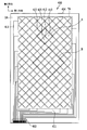
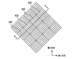
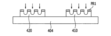
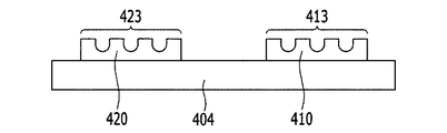
400:タッチパネル
404:タッチ基板
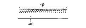
410:第1タッチ電極
411:第1タッチ配線
412:第1連結部
413:第1微細突起
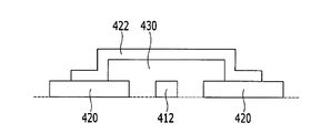
420:第2タッチ電極
421:第2タッチ配線
422:第2連結部
423:第2微細突起
430:絶縁膜
Claims (15)
- タッチ基板と、
第1方向に延長形成される複数の第1タッチ電極と、
前記第1方向に垂直な第2方向に延長形成される複数の第2タッチ電極と、を備え、
前記複数の第1および第2タッチ電極は、前記タッチ基板の同一面に形成されるか、前記タッチ基板の互いに異なる面にそれぞれ形成され、
前記複数の第1および第2タッチ電極のうち少なくとも一つには、複数の突起が形成され、
前記第1および第2タッチ電極のそれぞれは、前記タッチ基板と向かい合う第1面および前記第1面に対向する第2面を備え、
前記複数の突起は、前記第2面に形成され、
前記突起は繊毛形状であり、
前記第1および第2タッチ電極の本体部と前記突起は、同一の金属材料によって一体に形成されている、タッチセンサ。 - 前記第1および第2タッチ電極は、金属ナノワイヤーまたはメタルメッシュを含む、請求項1に記載のタッチセンサ。
- タッチ基板と、
第1方向に延長形成される複数の第1タッチ電極と、
前記第1方向に垂直な第2方向に延長形成される複数の第2タッチ電極と、を備え、
前記複数の第1および第2タッチ電極は、前記タッチ基板の同一面に形成されるか、前記タッチ基板の互いに異なる面にそれぞれ形成され、
前記複数の第1および第2タッチ電極のうち少なくとも一つには、複数の突起が形成され、
前記第1および第2タッチ電極のそれぞれは、前記タッチ基板と向かい合う第1面および前記第1面に対向する第2面を備え、
前記複数の突起は、前記第2面に形成され、
前記突起は繊毛形状であり、
前記突起の端部は、複数本に分かれた、タッチセンサ。 - 前記第1および第2タッチ電極は、金属ナノワイヤー、メタルメッシュ、炭素ナノチューブ、グラフェン、ITOおよびIZOのうち少なくとも一つを含む、請求項3に記載のタッチセンサ。
- 前記複数の突起は、前記タッチ基板に対して一定の角度に傾いた、請求項1から4のいずれか1項に記載のタッチセンサ。
- 前記複数の第1および第2タッチ電極は、前記タッチ基板の同一面に形成され、
前記複数の第1タッチ電極は、前記第1方向に互いに離隔した状態で配置され、
前記複数の第2タッチ電極は、前記第2方向に互いに離隔した状態で配置され、前記複数の第1タッチ電極と重ならない、請求項1から5のいずれか1項に記載のタッチセンサ。 - 前記複数の第1および第2タッチ電極は、同一層に形成される、請求項6に記載のタッチセンサ。
- 前記複数の第1タッチ電極のうち隣接した一対の第1タッチ電極は、第1連結部によって互いに連結され、
前記複数の第2タッチ電極のうち隣接した一対の第2タッチ電極は、前記第1連結部と離れた状態で交差する第2連結部によって互いに連結される、請求項7に記載のタッチセンサ。 - 前記第1連結部は、前記第1タッチ電極と同一層に形成される、請求項8に記載のタッチセンサ。
- 前記第1連結部は、前記第1タッチ電極と一体で形成される、請求項9に記載のタッチセンサ。
- 前記第2連結部は、前記第2タッチ電極と異なる層に形成される、請求項8から10のいずれか1項に記載のタッチセンサ。
- 前記第1および第2連結部の間に形成され、前記第1および第2連結部を絶縁する絶縁膜をさらに備える、請求項11に記載のタッチセンサ。
- 前記第2連結部の上面に複数の突起が形成される、請求項8から12のいずれか1項に記載のタッチセンサ。
- 前記複数の第1および第2タッチ電極は、前記タッチ基板の互いに異なる面に、互いに交差するように形成される、
請求項1から5のいずれか1項に記載のタッチセンサ。 - 前記第1および第2タッチ電極にそれぞれ連結された第1および第2タッチ配線をさらに備える、請求項1から14のいずれか1項に記載のタッチセンサ。
Applications Claiming Priority (2)
| Application Number | Priority Date | Filing Date | Title |
|---|---|---|---|
| KR10-2015-0026799 | 2015-02-25 | ||
| KR1020150026799A KR102281850B1 (ko) | 2015-02-25 | 2015-02-25 | 터치 센서, 그 제조 방법 및 이를 포함하는 표시 장치 |
Publications (2)
| Publication Number | Publication Date |
|---|---|
| JP2016157442A JP2016157442A (ja) | 2016-09-01 |
| JP6861468B2 true JP6861468B2 (ja) | 2021-04-21 |
Family
ID=55411324
Family Applications (1)
| Application Number | Title | Priority Date | Filing Date |
|---|---|---|---|
| JP2016033796A Active JP6861468B2 (ja) | 2015-02-25 | 2016-02-25 | タッチセンサ |
Country Status (5)
| Country | Link |
|---|---|
| US (1) | US10191578B2 (ja) |
| EP (1) | EP3062202B1 (ja) |
| JP (1) | JP6861468B2 (ja) |
| KR (1) | KR102281850B1 (ja) |
| CN (1) | CN105912152B (ja) |
Families Citing this family (15)
| Publication number | Priority date | Publication date | Assignee | Title |
|---|---|---|---|---|
| US9259904B2 (en) | 2011-10-20 | 2016-02-16 | Apple Inc. | Opaque thin film passivation |
| KR20150103977A (ko) * | 2014-03-04 | 2015-09-14 | 엘지이노텍 주식회사 | 터치 윈도우 및 이를 포함하는 디스플레이 장치 |
| EP3516489A1 (en) | 2016-09-23 | 2019-07-31 | Apple Inc. | Touch sensor panel with top and/or bottom shielding |
| KR102663715B1 (ko) | 2016-11-15 | 2024-05-16 | 삼성디스플레이 주식회사 | 표시 장치 및 이의 제조 방법 |
| KR102685973B1 (ko) * | 2016-12-14 | 2024-07-19 | 삼성디스플레이 주식회사 | 터치 센서 및 이를 포함하는 표시 장치 |
| US11127040B2 (en) | 2017-01-01 | 2021-09-21 | xAd, Inc. | Method and apparatus for real-time delivery of publicly displayed information to mobile devices |
| CN107036657B (zh) * | 2017-05-19 | 2019-08-16 | 重庆大学 | 一种磁、力纤毛仿生传感器的制备方法 |
| KR102360850B1 (ko) * | 2017-06-30 | 2022-02-10 | 삼성디스플레이 주식회사 | 터치 센서 및 이를 포함하는 표시 장치 |
| CN108319370B (zh) * | 2018-02-02 | 2021-11-23 | 合肥鑫晟光电科技有限公司 | 电子设备及其控制方法 |
| CN108925053B (zh) * | 2018-06-29 | 2020-05-22 | 武汉华星光电半导体显示技术有限公司 | 柔性线路板及其制作方法 |
| KR102758809B1 (ko) * | 2019-09-17 | 2025-01-23 | 엘지디스플레이 주식회사 | 터치 전극 제조용 마스크 |
| JP2021095648A (ja) * | 2019-12-14 | 2021-06-24 | 鳥光 慶一 | 離隔動作識別素子とこれを有する荷重刺激のセンシングシステム、及びこれらに関連する学習済みモデルと推測システム |
| CN114442832B (zh) * | 2020-11-04 | 2024-09-17 | 宸美(厦门)光电有限公司 | 触控面板及其制造方法 |
| US11675448B2 (en) | 2020-12-11 | 2023-06-13 | Tpk Advanced Solutions Inc. | Touch panel and method for forming the same |
| US12321559B1 (en) * | 2022-02-09 | 2025-06-03 | Apple Inc. | Flexible touch sensor panel with metal mesh and solid conductor |
Family Cites Families (20)
| Publication number | Priority date | Publication date | Assignee | Title |
|---|---|---|---|---|
| US7132161B2 (en) | 1999-06-14 | 2006-11-07 | Energy Science Laboratories, Inc. | Fiber adhesive material |
| DE10223234B4 (de) * | 2002-05-24 | 2005-02-03 | MAX-PLANCK-Gesellschaft zur Förderung der Wissenschaften e.V. | Verfahren zur Herstellung mikrostrukturierter Oberflächen mit gesteigerter Adhäsion und adhäsionssteigernd modifizierte Oberflächen |
| JP2005121908A (ja) | 2003-10-16 | 2005-05-12 | Advanced Display Inc | 反射型液晶表示装置および半透過型液晶表示装置ならびにこれらの製法 |
| US20080292840A1 (en) | 2004-05-19 | 2008-11-27 | The Regents Of The University Of California | Electrically and thermally conductive carbon nanotube or nanofiber array dry adhesive |
| KR101205852B1 (ko) | 2006-05-26 | 2012-11-28 | 엘아이지에이디피 주식회사 | 디스플레이 패널 제작을 위한 기판 합착 장치 및 방법,이에 사용되는 기판 흡착 장치 |
| KR101633034B1 (ko) * | 2009-10-23 | 2016-06-24 | 삼성디스플레이 주식회사 | 터치 기판, 이의 제조 방법 및 이를 갖는 표시 장치 |
| CN101852934A (zh) * | 2010-05-31 | 2010-10-06 | 北京富纳特创新科技有限公司 | 触摸式液晶显示屏 |
| CN103076913B (zh) * | 2010-07-22 | 2016-01-20 | 阿尔卑斯电气株式会社 | 输入装置及其制造方法 |
| KR20120091784A (ko) | 2011-02-10 | 2012-08-20 | 삼성전자주식회사 | 휴대용 통신 장치의 표시 장치 |
| JP5730240B2 (ja) | 2011-04-25 | 2015-06-03 | 信越ポリマー株式会社 | 静電容量センサシートの製造方法及び静電容量センサシート |
| JP5813875B2 (ja) | 2011-08-24 | 2015-11-17 | イノバ ダイナミックス, インコーポレイテッド | パターン化された透明導体および関連する製造方法 |
| EP2752867B1 (en) | 2011-08-31 | 2019-01-02 | Soken Chemical & Engineering Co., Ltd. | Adhesive sheet for immobilizing imprint mold, imprint device, and imprint method |
| TWM425340U (en) | 2011-10-21 | 2012-03-21 | Henghao Technology Co Ltd | Capacitive touch panel and touch display panel using the same |
| JP5293843B2 (ja) | 2012-01-24 | 2013-09-18 | デクセリアルズ株式会社 | 透明導電性素子、入力装置、電子機器および透明導電性素子作製用原盤 |
| KR102009880B1 (ko) * | 2012-10-23 | 2019-08-12 | 엘지디스플레이 주식회사 | 메탈 메쉬형 터치 스크린 패널 |
| US9632542B2 (en) * | 2013-05-02 | 2017-04-25 | The Boeing Company | Touch screens comprising graphene layers |
| CN104571652B (zh) * | 2013-10-09 | 2017-12-01 | 宸鸿光电科技股份有限公司 | 触控装置结构 |
| KR102211968B1 (ko) | 2013-12-02 | 2021-02-05 | 삼성디스플레이 주식회사 | 터치 패널, 표시 장치 및 터치 패널의 제조 방법 |
| CN106462304B (zh) * | 2014-05-12 | 2019-05-31 | Lg伊诺特有限公司 | 触摸窗 |
| CN104281319A (zh) * | 2014-08-22 | 2015-01-14 | 京东方科技集团股份有限公司 | 触摸面板及其制造方法和触摸显示装置 |
-
2015
- 2015-02-25 KR KR1020150026799A patent/KR102281850B1/ko active Active
-
2016
- 2016-01-07 US US14/990,753 patent/US10191578B2/en active Active
- 2016-02-25 JP JP2016033796A patent/JP6861468B2/ja active Active
- 2016-02-25 CN CN201610105602.2A patent/CN105912152B/zh active Active
- 2016-02-25 EP EP16157445.4A patent/EP3062202B1/en active Active
Also Published As
| Publication number | Publication date |
|---|---|
| EP3062202A1 (en) | 2016-08-31 |
| KR102281850B1 (ko) | 2021-07-26 |
| US10191578B2 (en) | 2019-01-29 |
| KR20160104188A (ko) | 2016-09-05 |
| CN105912152A (zh) | 2016-08-31 |
| CN105912152B (zh) | 2021-02-09 |
| EP3062202B1 (en) | 2021-05-12 |
| JP2016157442A (ja) | 2016-09-01 |
| US20160246435A1 (en) | 2016-08-25 |
Similar Documents
| Publication | Publication Date | Title |
|---|---|---|
| JP6861468B2 (ja) | タッチセンサ | |
| KR102373330B1 (ko) | 터치 센서를 포함하는 표시 장치 및 그 제조 방법 | |
| JP7023904B2 (ja) | タッチセンサを含む表示装置 | |
| CN102693036B (zh) | 制造用于触摸屏的透明电路基板的方法 | |
| CN103576949B (zh) | 触控面板及其制造方法 | |
| KR102262470B1 (ko) | 터치 스크린 패널 제조 방법 | |
| CN104850288B (zh) | 触摸窗以及具有触摸窗的触摸装置 | |
| KR20140095279A (ko) | 터치 및 휨 감지 기능을 가지는 플렉서블 표시장치 | |
| US20130271388A1 (en) | Touch sensing three-dimensional display device | |
| CN105630226A (zh) | 触摸窗 | |
| CN113496655B (zh) | 显示设备 | |
| KR102305463B1 (ko) | 터치 센서를 포함하는 표시 장치 및 그 구동 방법 | |
| KR20160120401A (ko) | 터치 스크린 패널, 이를 포함하는 표시 장치 및 그 구동 방법 | |
| TW201523367A (zh) | 觸控面板 | |
| KR102302824B1 (ko) | 터치 윈도우 및 터치 디바이스 | |
| KR20160073278A (ko) | 터치 센서 장치 및 이를 포함하는 표시 장치 | |
| KR102237815B1 (ko) | 터치 윈도우 | |
| KR20160016138A (ko) | 터치 윈도우 및 이를 포함하는 터치 디바이스 |
Legal Events
| Date | Code | Title | Description |
|---|---|---|---|
| RD02 | Notification of acceptance of power of attorney |
Free format text: JAPANESE INTERMEDIATE CODE: A7422 Effective date: 20170425 |
|
| A621 | Written request for application examination |
Free format text: JAPANESE INTERMEDIATE CODE: A621 Effective date: 20190109 |
|
| A977 | Report on retrieval |
Free format text: JAPANESE INTERMEDIATE CODE: A971007 Effective date: 20200122 |
|
| A131 | Notification of reasons for refusal |
Free format text: JAPANESE INTERMEDIATE CODE: A131 Effective date: 20200212 |
|
| A521 | Request for written amendment filed |
Free format text: JAPANESE INTERMEDIATE CODE: A523 Effective date: 20200511 |
|
| A02 | Decision of refusal |
Free format text: JAPANESE INTERMEDIATE CODE: A02 Effective date: 20200923 |
|
| A521 | Request for written amendment filed |
Free format text: JAPANESE INTERMEDIATE CODE: A523 Effective date: 20210119 |
|
| C60 | Trial request (containing other claim documents, opposition documents) |
Free format text: JAPANESE INTERMEDIATE CODE: C60 Effective date: 20210119 |
|
| A911 | Transfer to examiner for re-examination before appeal (zenchi) |
Free format text: JAPANESE INTERMEDIATE CODE: A911 Effective date: 20210127 |
|
| C21 | Notice of transfer of a case for reconsideration by examiners before appeal proceedings |
Free format text: JAPANESE INTERMEDIATE CODE: C21 Effective date: 20210202 |
|
| TRDD | Decision of grant or rejection written | ||
| A01 | Written decision to grant a patent or to grant a registration (utility model) |
Free format text: JAPANESE INTERMEDIATE CODE: A01 Effective date: 20210302 |
|
| A61 | First payment of annual fees (during grant procedure) |
Free format text: JAPANESE INTERMEDIATE CODE: A61 Effective date: 20210330 |
|
| R150 | Certificate of patent or registration of utility model |
Ref document number: 6861468 Country of ref document: JP Free format text: JAPANESE INTERMEDIATE CODE: R150 |
|
| R250 | Receipt of annual fees |
Free format text: JAPANESE INTERMEDIATE CODE: R250 |
|
| R250 | Receipt of annual fees |
Free format text: JAPANESE INTERMEDIATE CODE: R250 |