JP6853034B2 - Optical semiconductor device storage package and optical semiconductor device - Google Patents

Optical semiconductor device storage package and optical semiconductor device Download PDF

Info

Publication number
JP6853034B2
JP6853034B2 JP2016249431A JP2016249431A JP6853034B2 JP 6853034 B2 JP6853034 B2 JP 6853034B2 JP 2016249431 A JP2016249431 A JP 2016249431A JP 2016249431 A JP2016249431 A JP 2016249431A JP 6853034 B2 JP6853034 B2 JP 6853034B2
Authority
JP
Japan
Prior art keywords
substrate
optical semiconductor
input
insulating layer
support portion
Prior art date
Legal status (The legal status is an assumption and is not a legal conclusion. Google has not performed a legal analysis and makes no representation as to the accuracy of the status listed.)
Active
Application number
JP2016249431A
Other languages
Japanese (ja)
Other versions
JP2017120901A (en
Inventor
宮石 学
学 宮石
Current Assignee (The listed assignees may be inaccurate. Google has not performed a legal analysis and makes no representation or warranty as to the accuracy of the list.)
Kyocera Corp
Original Assignee
Kyocera Corp
Priority date (The priority date is an assumption and is not a legal conclusion. Google has not performed a legal analysis and makes no representation as to the accuracy of the date listed.)
Filing date
Publication date
Application filed by Kyocera Corp filed Critical Kyocera Corp
Publication of JP2017120901A publication Critical patent/JP2017120901A/en
Application granted granted Critical
Publication of JP6853034B2 publication Critical patent/JP6853034B2/en
Active legal-status Critical Current
Anticipated expiration legal-status Critical

Links

Images

Description

本発明は、光半導体素子を収容するための光半導体素子収納用パッケージおよび光半導体装置に関する。 The present invention relates to a package for accommodating an optical semiconductor element and an optical semiconductor device for accommodating the optical semiconductor element.

光通信の分野等で使用される半導体レーザダイオードまたはフォトダイオード等の光半導体素子は、光半導体素子収納用パッケージ(以下、パッケージともいう)に収納される。例示的な光半導体素子収納用パッケージは、上面に光半導体素子が載置される載置部を有する基板と、該基板の上面に前記載置部を囲繞するように接合される枠体とを備える。 An optical semiconductor element such as a semiconductor laser diode or a photodiode used in the field of optical communication or the like is housed in a package for storing the optical semiconductor element (hereinafter, also referred to as a package). An exemplary optical semiconductor device storage package comprises a substrate having a mounting portion on which the optical semiconductor element is mounted on the upper surface and a frame body joined on the upper surface of the substrate so as to surround the previously described mounting portion. Be prepared.

特開2004-119805号公報Japanese Unexamined Patent Publication No. 2004-119805

光半導体素子収納用パッケージにおいて、パッケージ内に収納された光半導体素子と外部回路との間の入出力信号を伝送するために、枠体に切欠き部を設け、絶縁材料から成り、入出力信号を伝送するための信号線路を有する入出力端子を前記切欠き部に挿入固定するとともに、入出力端子が挿入固定された枠体と基板とを接合する場合がある。 In the optical semiconductor element storage package, in order to transmit the input / output signal between the optical semiconductor element housed in the package and the external circuit, a notch is provided in the frame, and the input / output signal is made of an insulating material. An input / output terminal having a signal line for transmitting a signal may be inserted and fixed in the notch portion, and a frame body into which the input / output terminal is inserted and fixed may be joined to the substrate.

しかしながら、基板および枠体が金属材料から成り、入出力端子がセラミックス等の材料から成る場合、入出力端子が挿入固定された枠体と基板とを接合するための加熱、冷却の際に、基板と枠体と入出力端子との間の熱伝導率、ヤング率、および熱膨張係数の差によって生じる内部応力によって、光半導体素子収納用パッケージが破損する、特に入出力端子の角部にクラックが発生する虞があるという問題があった。 However, when the substrate and the frame are made of a metal material and the input / output terminals are made of a material such as ceramics, the substrate is heated and cooled to join the frame and the substrate to which the input / output terminals are inserted and fixed. The internal stress caused by the difference in thermal conductivity, Young's modulus, and coefficient of thermal expansion between the frame and the input / output terminals damages the optical semiconductor device storage package, especially cracks at the corners of the input / output terminals. There was a problem that it might occur.

本発明の光半導体素子収納用パッケージは、主面に光半導体素子が載置される載置部を有する基板と、前記基板の前記主面に接合される枠体であって、平面視して前記載置部を囲繞するように設けられ、前記基板側から切り欠かれた切欠き部を有する枠部と、前記切欠き部に挿入固定されているとともに、前記主面の面方向において一部分が前記基板の外方に張出している入出力端子とを含む枠体と、前記入出力端子の前記一部分に、前記主面の面方向に前記基板と間隔を空けて設けられている支持部とを備える。このとき、前記入出力端子および前記支持部の熱伝導率が、前記基板の熱伝導率よりも小さくてもよい。また、前記支持部のヤング率が、前記基板および前記入出力端子のヤング率よりも小さくてもよい。また、前記支持部の熱膨張係数が、前記基板および前記入出力端子の熱膨張係数よりも小さくてもよい。 The optical semiconductor element storage package of the present invention is a substrate having a mounting portion on which the optical semiconductor element is mounted on the main surface and a frame body joined to the main surface of the substrate, and is viewed in a plan view. A frame portion that is provided so as to surround the above-described mounting portion and has a notch portion notched from the substrate side, and is inserted and fixed in the notch portion, and a part thereof is inserted and fixed in the surface direction of the main surface. A frame including an input / output terminal overhanging the outside of the substrate, and a support portion provided on the part of the input / output terminal at a distance from the substrate in the surface direction of the main surface. Be prepared. At this time, the thermal conductivity of the input / output terminal and the support portion may be smaller than the thermal conductivity of the substrate. Further, the Young's modulus of the support portion may be smaller than the Young's modulus of the substrate and the input / output terminals. Further, the coefficient of thermal expansion of the support portion may be smaller than the coefficient of thermal expansion of the substrate and the input / output terminals.

また、本発明の光半導体装置は、前述の光半導体素子収納用パッケージと、前記基板の前記載置部に載置用基台を介して載置される光半導体素子と、前記枠体に接合される蓋体とを備える。 Further, the optical semiconductor device of the present invention is joined to the above-mentioned optical semiconductor element accommodating package, the optical semiconductor element mounted on the pre-described mounting portion of the substrate via a mounting base, and the frame body. It is provided with a lid to be used.

本発明の光半導体素子収納用パッケージによれば、基板と枠体とを接合するための加熱、冷却の際に、基板と枠部と入出力端子との間の熱伝導率、ヤング率、および熱膨張係数の差によって生じる内部応力を緩和して、光半導体素子収納用パッケージの破損、特に入出力端子におけるクラックの発生を抑制することができ、それによって、光半導体素子収納用パッケージの信頼性を向上することができる。 According to the optical semiconductor device storage package of the present invention, the thermal conductivity, Young's ratio, and the thermal conductivity between the substrate, the frame, and the input / output terminals during heating and cooling for joining the substrate and the frame, and The internal stress caused by the difference in thermal expansion coefficient can be alleviated, and damage to the optical semiconductor device storage package, especially cracks at the input / output terminals, can be suppressed, whereby the reliability of the optical semiconductor device storage package can be suppressed. Can be improved.

本発明の光半導体装置によれば、基板と枠体とを接合するための加熱、冷却の際に、基
板と枠部と入出力端子との間の熱伝導率、ヤング率、および熱膨張係数の差によって生じる内部応力を緩和して、光半導体素子収納用パッケージの破損、特に入出力端子におけるクラックの発生を抑制することができる。さらに、本発明の光半導体装置によれば、蓋体と枠体とを接合するための加熱、冷却の際に、基板と枠部と入出力端子との間の熱伝導率、ヤング率、および熱膨張係数の差によって生じる内部応力を緩和して、素子収納用パッケージの破損、特に入出力端子におけるクラックの発生を抑制することができる。したがって、本発明の光半導体装置によれば、信頼性の向上した光半導体装置を提供することができる。
According to the optical semiconductor device of the present invention, the thermal conductivity, Young's modulus, and coefficient of thermal expansion between the substrate, the frame, and the input / output terminals during heating and cooling for joining the substrate and the frame. It is possible to alleviate the internal stress caused by the difference between the above and suppress the damage of the optical semiconductor element storage package, particularly the occurrence of cracks in the input / output terminals. Further, according to the optical semiconductor device of the present invention, the thermal conductivity, Young's modulus, and the Young's modulus between the substrate, the frame portion, and the input / output terminals during heating and cooling for joining the lid body and the frame body, and By relaxing the internal stress caused by the difference in the coefficient of thermal expansion, it is possible to suppress damage to the device storage package, particularly cracks at the input / output terminals. Therefore, according to the optical semiconductor device of the present invention, it is possible to provide an optical semiconductor device with improved reliability.

(a)は、本発明の実施形態の光半導体素子収納用パッケージを枠部側から視た斜視図であり、(b)は、本発明の実施形態の光半導体素子収納用パッケージを入出力端子側から視た斜視図である。(A) is a perspective view of the optical semiconductor element storage package of the embodiment of the present invention as viewed from the frame portion side, and (b) is an input / output terminal of the optical semiconductor element storage package of the embodiment of the present invention. It is a perspective view seen from the side. 本発明の実施形態の光半導体素子収納用パッケージを示す分解斜視図である。It is an exploded perspective view which shows the optical semiconductor element accommodating package of embodiment of this invention. (a)は、発明の実施形態の光半導体素子収納用パッケージを示す平面図であり、(b)は、発明の実施形態の光半導体素子収納用パッケージを示す底面図である。(A) is a plan view showing the optical semiconductor device storage package of the embodiment of the invention, and (b) is a bottom view showing the optical semiconductor device storage package of the embodiment of the invention. (c)は、本発明の実施形態の光半導体素子収納用パッケージを示す側面図である。(C) is a side view which shows the optical semiconductor element accommodating package of embodiment of this invention. 図3A(a)に示すX−X線における断面図である。3 is a cross-sectional view taken along the line XX shown in FIG. 3A (a). (a),(b)は、本発明の変形例の光半導体素子収納用パッケージを示す側面図である。(A) and (b) are side views which show the optical semiconductor element accommodating package of the modification of this invention. (c),(d)は、本発明の変形例の光半導体素子収納用パッケージを示す側面図である。(C) and (d) are side views which show the optical semiconductor element accommodating package of the modification of this invention. (a)は、本発明の変形例の光半導体素子収納用パッケージを枠部側から視た斜視図であり、(b)は、本発明の変形例の光半導体素子収納用パッケージを入出力端子側から視た斜視図である。(A) is a perspective view of the optical semiconductor element storage package of the modified example of the present invention as viewed from the frame side, and (b) is the input / output terminal of the optical semiconductor element storage package of the modified example of the present invention. It is a perspective view seen from the side. 図6に示す光半導体素子収納用パッケージを分解して示す分解斜視図である。It is an exploded perspective view which shows by disassembling the package for accommodating an optical semiconductor element shown in FIG. (a)〜(d)は、それぞれ本発明の変形例の光半導体素子収納用パッケージを示す底面図である。(A) to (d) are bottom views which show the optical semiconductor element accommodating package of the modification of this invention respectively. 本発明の光半導体装置を示す断面図である。It is sectional drawing which shows the optical semiconductor device of this invention.

本発明の光半導体素子収納用パッケージについて、図面を参照して説明する。 The package for accommodating an optical semiconductor element of the present invention will be described with reference to the drawings.

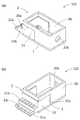
図1〜図4を参照して、本発明の実施形態の光半導体素子収納用パッケージ100について説明する。 The optical semiconductor device storage package 100 according to the embodiment of the present invention will be described with reference to FIGS. 1 to 4.

本発明の光半導体素子収納用パッケージ100は、主面1aに光半導体素子4が載置される載置部1bを有する基板1と、基板1の主面に接合される枠体2と、支持部3とを備える。枠体2は、平面視して載置部1bを囲繞するように設けられ、基板1側から切り欠かれた切欠き部20aを有する枠部20と、切欠き部20aに挿入固定されているとともに、基板1の主面1aの面方向において一部分が基板1の外方に張出している入出力端子21とを含む。支持部3は、基板1の外方に張出している入出力端子21の一部分に、基板1の主面1aの面方向に基板1と間隔を空けて設けられる。 The optical semiconductor element storage package 100 of the present invention supports a substrate 1 having a mounting portion 1b on which the optical semiconductor element 4 is mounted on the main surface 1a, a frame body 2 joined to the main surface of the substrate 1, and a support. It includes a part 3. The frame body 2 is provided so as to surround the mounting portion 1b in a plan view, and is inserted and fixed to the frame portion 20 having the notch portion 20a cut out from the substrate 1 side and the notch portion 20a. At the same time, it includes an input / output terminal 21 whose part extends outward from the substrate 1 in the plane direction of the main surface 1a of the substrate 1. The support portion 3 is provided on a part of the input / output terminals 21 extending outward from the substrate 1 at intervals from the substrate 1 in the surface direction of the main surface 1a of the substrate 1.

基板1は、光半導体素子4を支持するための支持部材、および光半導体素子4で発生した熱を放散するための放熱板として機能する。また、基板1は、Cu−W合金やFe−N
i−Co合金等の金属から成るが、Cu−W合金から成るのが好ましい。基板1は、そのインゴットに圧延加工や打ち抜き加工等の従来周知の金属加工法を施すことによって所定形状に成形され製作される。また、その表面に耐蝕性に優れかつロウ材との濡れ性に優れる金属、具体的には厚さ0.5〜9μmのNi層と厚さ0.5〜9μmのAu層を順次メッキ法により被着させておくのがよく、それによって、基板1が酸化腐食するのを有効に防止することができるとともに、基板1上面に載置用基台5を介して光半導体素子4を強固に接合できる。
The substrate 1 functions as a support member for supporting the optical semiconductor element 4 and a heat radiating plate for dissipating the heat generated by the optical semiconductor element 4. Further, the substrate 1 is a Cu-W alloy or Fe-N.
It is made of a metal such as an i-Co alloy, but is preferably made of a Cu-W alloy. The substrate 1 is formed and manufactured into a predetermined shape by subjecting the ingot to a conventionally known metal processing method such as rolling or punching. Further, a metal having excellent corrosion resistance and excellent wettability with a brazing material, specifically, a Ni layer having a thickness of 0.5 to 9 μm and an Au layer having a thickness of 0.5 to 9 μm are sequentially plated on the surface thereof by a plating method. It is preferable to adhere to the substrate 1, whereby the substrate 1 can be effectively prevented from being oxidatively corroded, and the optical semiconductor element 4 is firmly bonded to the upper surface of the substrate 1 via the mounting base 5. it can.

枠体2の枠部20は、平面視して基板1の載置部1bを囲繞するように設けられるとともに、基板1側から切り欠かれた切欠き部20aを有する。枠部20が、平面視して矩形枠状の形状を有し、切欠き部20aが、枠部20の4つの側壁のうちの1つの側壁に形成されてもよく、隣接する2つの側壁に連続して形成されてもよく、3つの側壁に連続して形成されてもよい。 The frame portion 20 of the frame body 2 is provided so as to surround the mounting portion 1b of the substrate 1 in a plan view, and has a notch portion 20a cut out from the substrate 1 side. The frame portion 20 has a rectangular frame-like shape in a plan view, and the notch portion 20a may be formed on one side wall of the four side walls of the frame portion 20, and may be formed on two adjacent side walls. It may be formed continuously, or it may be formed continuously on three side walls.

枠部20は、基板1との接合を強固にするとともに光半導体パッケージの外部に対する電磁遮蔽を行なうために、Fe−Ni−Co合金やFe−Ni合金等の金属から成るが、Fe−Ni−Co合金から成るのが好ましい。枠部20は、基板1と同様にその材料のインゴットに圧延加工や打ち抜き加工等の従来周知の金属加工法を施すことにより所定形状に成形され製作される。枠部20は、ドリルによる孔あけ加工等により形成される光ファイバを挿入するための貫通孔20bを有してもよい。貫通孔20bの枠体2外側開口の周囲に筒状の固定部材の一端が接合されるかまたは貫通孔20bに固定部材が嵌着接合されてもよい。 The frame portion 20 is made of a metal such as a Fe—Ni—Co alloy or a Fe—Ni alloy in order to strengthen the bond with the substrate 1 and electromagnetically shield the outside of the optical semiconductor package. It is preferably made of a Co alloy. Similar to the substrate 1, the frame portion 20 is formed and manufactured into a predetermined shape by subjecting an ingot of the material to a conventionally known metal processing method such as rolling or punching. The frame portion 20 may have a through hole 20b for inserting an optical fiber formed by drilling or the like. One end of the tubular fixing member may be joined around the outer opening of the frame body 2 of the through hole 20b, or the fixing member may be fitted and joined to the through hole 20b.

枠部20の表面には、耐蝕性に優れかつロウ材との濡れ性に優れる金属、具体的には厚さ0.5〜9μmのNi層と厚さ0.5〜9μmのAu層をメッキ法により順次被着させておくことが好ましく、それによって、枠部20が酸化腐食するのを有効に防止するとともに枠部20に固定部材を強固に接合できる。 The surface of the frame portion 20 is plated with a metal having excellent corrosion resistance and excellent wettability with a brazing material, specifically, a Ni layer having a thickness of 0.5 to 9 μm and an Au layer having a thickness of 0.5 to 9 μm. It is preferable that the frames are sequentially adhered by a method, whereby the frame portion 20 can be effectively prevented from being oxidatively corroded and the fixing member can be firmly joined to the frame portion 20.

枠体2の入出力端子21は、切欠き部20aに挿入固定されているとともに、基板1の主面1aの面方向において一部分が基板1の外方に張出している。入出力端子21は、絶縁材料から成り、例えば酸化アルミニウム質焼結体、ムライト質焼結体、炭化珪素質焼結体、窒化アルミニウム質焼結体、窒化珪素質焼結体またはガラスセラミックス等のセラミック材料から成る。入出力端子21は、パッケージ内に収納された光半導体素子と外部回路との間の入出力信号を伝送するための信号線路21cを有する。 The input / output terminal 21 of the frame body 2 is inserted and fixed in the notch portion 20a, and a part thereof projects outward of the substrate 1 in the surface direction of the main surface 1a of the substrate 1. The input / output terminal 21 is made of an insulating material, for example, an aluminum oxide sintered body, a mullite sintered body, a silicon carbide sintered body, an aluminum nitride material sintered body, a silicon nitride material sintered body, a glass ceramic, or the like. Made of ceramic material. The input / output terminal 21 has a signal line 21c for transmitting an input / output signal between the optical semiconductor element housed in the package and an external circuit.

入出力端子21は、複数の絶縁層が積層されてなる積層体を含んで構成されてもよい。例えば、図2に示すように、入出力端子21は、矩形形状の第1絶縁層21aと、第1絶縁層21a上であって第1絶縁層21aの上面のうち枠部20から外方に遠ざかった箇所が露出するように設けられた矩形形状の第2絶縁層21bとを含んで構成されてもよく、信号線路21cは、第1絶縁層21a上と第2絶縁層21b上とに設けられてもよい。 The input / output terminal 21 may be configured to include a laminated body in which a plurality of insulating layers are laminated. For example, as shown in FIG. 2, the input / output terminal 21 is on the rectangular first insulating layer 21a and the first insulating layer 21a, and is outward from the frame portion 20 of the upper surface of the first insulating layer 21a. It may be configured to include a rectangular-shaped second insulating layer 21b provided so as to expose a distant portion, and the signal line 21c is provided on the first insulating layer 21a and the second insulating layer 21b. May be done.

支持部3は、基板1の外方に張出している入出力端子21の一部分に、基板1の主面1aの面方向に基板1と間隔を空けて設けられる。入出力端子21が第1絶縁層21aと第2絶縁層21bとの積層体を含んで構成される場合には、支持部3は、平面視して第1絶縁層21aだけに重なるように、第1絶縁層21aの下面に設けられることが好ましく、さらに、第1絶縁層21aの下面が、基板1の主面1aと同じ高さに位置するとともに、支持部3の厚みが、基板1の厚みと一致することが好ましい。これにより、第1絶縁層21aの露出する上面に設けられた信号線路21cに、フレキシブルプリント回路基板等の外部回路に設けられた電極部を、はんだ等の導電性部材で電気的に接続する際に、主面1aに対して直角方向かつ第1絶縁層21aから支持部3の方向に加えられる外力によって生じる、入出力端子21内の内部応力を低減することができる。なお、支持部3の厚みが、基板1の厚みより薄い場合には、信号線路21cと外部回路とを電気的に接続するための外力が入出力端子21に加えられる際に、支持部3が光半導体装置200を載置する載置基板と接触せず、支持部3が入出力端子21を支持することができないことから、入出力端子21内に生じる内部応力が増加する。また、支持部3の厚みが、基板1の厚みより厚い場合には、光半導体装置200を実装基板に実装する際に、基板1と実装基板との間に空隙が発生することから、光半導体素子収納用パッケージ100に収納される光半導体素子4から生じる熱を、基板1を介して効率よく実装基板に伝達し、光半導体素子収納用パッケージ100の外部に放熱することができない。また、支持部3は、Cu−W合金やFe−Ni−Co合金等の金属から成るが、Fe−Ni−Co合金から成るのが好ましい。これにより、光半導体素子収納用パッケージ100を加熱、冷却して組み立てる際に、入出力端子21と支持部3との熱膨張係数の差によって生じる内部応力を緩和できるとともに、入出力端子21の変形に伴って生じる内部応力を小さくでき、さらに、入出力端子21内の内部応力が一部に集中したり、増加したりすることを抑制できる。その結果、入出力端子21におけるクラックの発生を抑制することができる。 The support portion 3 is provided on a part of the input / output terminals 21 extending outward from the substrate 1 at intervals from the substrate 1 in the surface direction of the main surface 1a of the substrate 1. When the input / output terminal 21 includes a laminate of the first insulating layer 21a and the second insulating layer 21b, the support portion 3 is arranged so as to overlap only the first insulating layer 21a in a plan view. It is preferable that the lower surface of the first insulating layer 21a is provided, and further, the lower surface of the first insulating layer 21a is located at the same height as the main surface 1a of the substrate 1, and the thickness of the support portion 3 is the thickness of the substrate 1. It is preferable to match the thickness. As a result, when the electrode portion provided in the external circuit such as the flexible printed circuit board is electrically connected to the signal line 21c provided on the exposed upper surface of the first insulating layer 21a with a conductive member such as solder. In addition, the internal stress in the input / output terminal 21 generated by the external force applied in the direction perpendicular to the main surface 1a and in the direction from the first insulating layer 21a to the support portion 3 can be reduced. When the thickness of the support portion 3 is thinner than the thickness of the substrate 1, the support portion 3 is applied to the input / output terminal 21 when an external force for electrically connecting the signal line 21c and the external circuit is applied to the input / output terminal 21. Since the support portion 3 cannot support the input / output terminals 21 without coming into contact with the mounting substrate on which the optical semiconductor device 200 is mounted, the internal stress generated in the input / output terminals 21 increases. Further, when the thickness of the support portion 3 is thicker than the thickness of the substrate 1, a gap is generated between the substrate 1 and the mounting substrate when the optical semiconductor device 200 is mounted on the mounting substrate. Therefore, the optical semiconductor The heat generated from the optical semiconductor element 4 stored in the element storage package 100 cannot be efficiently transferred to the mounting substrate via the substrate 1 and dissipated to the outside of the optical semiconductor element storage package 100. The support portion 3 is made of a metal such as a Cu—W alloy or a Fe—Ni—Co alloy, but is preferably made of a Fe—Ni—Co alloy. As a result, when the optical semiconductor element storage package 100 is heated, cooled and assembled, the internal stress caused by the difference in the coefficient of thermal expansion between the input / output terminal 21 and the support portion 3 can be alleviated, and the input / output terminal 21 is deformed. The internal stress generated in association with the above can be reduced, and further, it is possible to prevent the internal stress in the input / output terminal 21 from being partially concentrated or increased. As a result, the occurrence of cracks in the input / output terminals 21 can be suppressed.

このような構成によって、基板1と枠体2とを銀ロウ等のロウ材を介して接合するための加熱、冷却の際に、基板1と枠部20と入出力端子21との間の熱伝導率、ヤング率、および熱膨張係数の差によって生じる内部応力を緩和して、光半導体素子収納用パッケージの破損、特に入出力端子21におけるクラックの発生を抑制することができ、それによって、光半導体素子収納用パッケージの信頼性を向上することができる。 With such a configuration, the heat between the substrate 1 and the frame portion 20 and the input / output terminal 21 is generated during heating and cooling for joining the substrate 1 and the frame 2 via a brazing material such as silver brazing. Internal stresses caused by differences in conductivity, Young's modulus, and coefficient of thermal expansion can be alleviated to prevent damage to the optical semiconductor device storage package, especially cracks in the input / output terminals 21, thereby producing light. The reliability of the semiconductor element storage package can be improved.

また、本実施形態の光半導体素子収納用パッケージ100において、基板1および支持部3は、各々、矩形形状を有し、基板1の一辺と、該一辺に対向する支持部3の辺とが平行になるように配置されてもよい。それによって、基板1と枠体2とを銀ロウ等のロウ材を介して接合するための加熱、冷却の際に生じる内部応力が、光半導体素子収納用パッケージ100の特定の部分に集中することを抑制することができる。 Further, in the optical semiconductor element storage package 100 of the present embodiment, the substrate 1 and the support portion 3 each have a rectangular shape, and one side of the substrate 1 and the side of the support portion 3 facing the one side are parallel to each other. It may be arranged so as to be. As a result, the internal stress generated during heating and cooling for joining the substrate 1 and the frame 2 via a brazing material such as silver wax is concentrated on a specific part of the optical semiconductor element housing package 100. Can be suppressed.

基板1、および支持部3は、同一の材料から成ってもよいが、異なる材料から成ってもよい。異なる材料から成る場合は、基板1、支持部3、および入出力端子21は、以下に示す熱伝導率、ヤング率、および熱膨張係数に関する条件を満たしていることが好ましい。 The substrate 1 and the support portion 3 may be made of the same material, but may be made of different materials. When made of different materials, it is preferable that the substrate 1, the support portion 3, and the input / output terminal 21 satisfy the following conditions regarding thermal conductivity, Young's modulus, and coefficient of thermal expansion.

基板1の熱伝導率は150〜400W/(m・K)であってもよく、入出力端子21の熱伝導率は10〜40W/(m・K)であってもよく、支持部3の熱伝導率は10〜20W/(m・K)であってもよいが、入出力端子21および支持部3の熱伝導率が、基板1の熱伝導率よりも小さいことが好ましい。これにより、光半導体素子収納用パッケージ100を加熱、冷却して組み立てる際に、入出力端子21に加えられた熱が支持部3を介して速やかに光半導体素子収納用パッケージ100の載置基板に放熱され難くなることから、入出力端子21と支持部3との熱膨張係数の差によって生じる内部応力の変動が緩やかになり、さらに、支持部3が緩やかに変形しながら内部応力を緩和できることから、入出力端子21におけるクラックの発生を抑制することができる。 The thermal conductivity of the substrate 1 may be 150 to 400 W / (m · K), the thermal conductivity of the input / output terminal 21 may be 10 to 40 W / (m · K), and the support portion 3 may have a thermal conductivity of 10 to 40 W / (m · K). The thermal conductivity may be 10 to 20 W / (m · K), but it is preferable that the thermal conductivity of the input / output terminal 21 and the support portion 3 is smaller than the thermal conductivity of the substrate 1. As a result, when the optical semiconductor element storage package 100 is heated, cooled, and assembled, the heat applied to the input / output terminals 21 is quickly applied to the mounting substrate of the optical semiconductor element storage package 100 via the support portion 3. Since it is difficult to dissipate heat, the fluctuation of the internal stress caused by the difference in the coefficient of thermal expansion between the input / output terminal 21 and the support portion 3 becomes gentle, and further, the internal stress can be relaxed while the support portion 3 is gently deformed. , Occurrence of cracks in the input / output terminal 21 can be suppressed.

基板1のヤング率は265〜310GPaであってもよく、入出力端子21のヤング率は270〜310GPaであってもよく、支持部3のヤング率は120〜150GPaであってもよいが、支持部3のヤング率が、基板1および入出力端子21のヤング率よりも小さいことが好ましい。これにより、光半導体素子収納用パッケージ100を加熱、冷却して組み立てる際に支持部3が変形しやすくなり、入出力端子21と支持部3との熱膨張係数の差によって生じる内部応力を支持部3によって緩和することができる。その結果、入出力端子21におけるクラックの発生を抑制することができる。 The Young's modulus of the substrate 1 may be 265 to 310 GPa, the Young's modulus of the input / output terminal 21 may be 270 to 310 GPa, and the Young's modulus of the support portion 3 may be 120 to 150 GPa, but the support It is preferable that the Young's modulus of the part 3 is smaller than the Young's modulus of the substrate 1 and the input / output terminal 21. As a result, the support portion 3 is easily deformed when the optical semiconductor element storage package 100 is heated, cooled, and assembled, and the internal stress generated by the difference in the coefficient of thermal expansion between the input / output terminal 21 and the support portion 3 is generated by the support portion. It can be alleviated by 3. As a result, the occurrence of cracks in the input / output terminals 21 can be suppressed.

基板1の熱膨張係数は5×10⁻⁶〜20×10−6/Kであってもよく、入出力端子21の熱膨張係数は5×10−6〜10×10−6/Kであってもよく、支持部3の熱膨張係数は4×10−6〜10×10−6/Kであってもよいが、支持部3の熱膨張係数が、基板1および入出力端子21の熱膨張係数よりも小さいことが好ましい。これにより、光半導体素子収納用パッケージ100を加熱、冷却して組み立てる際に、支持部3の熱膨張、熱収縮に伴って生じる入出力端子21の変形を抑制することができるとともに、この変形に伴って生じる、入出力端子21内の内部応力を小さくできる。その結果、入出力端子21におけるクラックの発生を抑制することができる。 The coefficient of thermal expansion of the substrate 1 may be 5 × 10 -6 to 20 × 10 -6 / K, and the coefficient of thermal expansion of the input / output terminal 21 is 5 × 10 -6 to 10 × 10 -6 / K. The coefficient of thermal expansion of the support portion 3 may be 4 × 10⁻⁶ to 10 × 10-6 / K, but the coefficient of thermal expansion of the support portion 3 is the heat of the substrate 1 and the input / output terminals 21. It is preferably smaller than the coefficient of expansion. As a result, when the optical semiconductor element storage package 100 is heated, cooled, and assembled, the deformation of the input / output terminal 21 caused by the thermal expansion and contraction of the support portion 3 can be suppressed, and the deformation can be suppressed. The internal stress in the input / output terminal 21 that accompanies this can be reduced. As a result, the occurrence of cracks in the input / output terminals 21 can be suppressed.

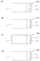
図5A、図5Bは、本発明の変形例の光半導体素子収納用パッケージ100A,100B,100C,100Dを示す。 5A and 5B show the optical semiconductor device storage packages 100A, 100B, 100C, and 100D of the modified example of the present invention.

図5A(a)に示すように、光半導体素子収納用パッケージ100Aは、支持部3Aが、平面視して入出力端子21の第1絶縁層21aおよび第2絶縁層21bの両方に重なるように構成される。これにより、第1絶縁層21aの露出する上面、または、第2絶縁層21bの露出する上面に設けられた信号線路21cに、フレキシブルプリント回路基板等の外部回路に設けられた電極部をはんだ等の導電性部材で電気的に接続する際に、主面1aに対して直角方向かつ第1絶縁層21aまたは第2絶縁層21bから支持部3の方向に加えられる外力によって生じる、入出力端子21内の内部応力が、枠体20の外側で第1絶縁層21aと第2絶縁層21bからなる角部に集中することを抑制できる。その結果、枠体20の外側で第1絶縁層21aと第2絶縁層21bからなる角部を起点とした、入出力端子21におけるクラックの発生を抑制することができる。 As shown in FIG. 5A (a), in the optical semiconductor element accommodating package 100A, the support portion 3A overlaps both the first insulating layer 21a and the second insulating layer 21b of the input / output terminal 21 in a plan view. It is composed. As a result, the electrode portion provided in the external circuit such as the flexible printed circuit board is soldered to the signal line 21c provided on the exposed upper surface of the first insulating layer 21a or the exposed upper surface of the second insulating layer 21b. The input / output terminal 21 generated by an external force applied in the direction perpendicular to the main surface 1a and in the direction from the first insulating layer 21a or the second insulating layer 21b to the support portion 3 when electrically connected by the conductive member of the above. It is possible to prevent the internal stress inside from concentrating on the corner portion composed of the first insulating layer 21a and the second insulating layer 21b on the outside of the frame body 20. As a result, it is possible to suppress the occurrence of cracks in the input / output terminal 21 starting from the corner portion composed of the first insulating layer 21a and the second insulating layer 21b on the outside of the frame body 20.

また、図5A(b)に示すように、光半導体素子収納用パッケージ100Bは、入出力端子21が張出する方向において、支持部3Bの端面と、第1絶縁層21aの端面とが平面視で重なるように構成される。これにより、第1絶縁層21aの露出する上面に設けられた信号線路21cに、フレキシブルプリント回路基板等の外部回路に設けられた電極部を、はんだ等の導電性部材で電気的に接続する際に、主面1aに対して直角方向かつ第1絶縁層21aから支持部3の方向に加えられる外力によって生じる、入出力端子21内の内部応力が、支持部3を起点としたテコの原理によって枠体20の外側で第1絶縁層21aと第2絶縁層21bからなる角部にて増加することを抑制できる。その結果、枠体20の外側で第1絶縁層21aと第2絶縁層21bからなる角部を起点とした、入出力端子21におけるクラックの発生を抑制することができる。 Further, as shown in FIG. 5A (b), in the optical semiconductor element storage package 100B, the end face of the support portion 3B and the end face of the first insulating layer 21a are viewed in a plan view in the direction in which the input / output terminals 21 project. It is configured to overlap with. As a result, when the electrode portion provided in the external circuit such as the flexible printed circuit board is electrically connected to the signal line 21c provided on the exposed upper surface of the first insulating layer 21a with a conductive member such as solder. In addition, the internal stress in the input / output terminal 21 generated by the external force applied in the direction perpendicular to the main surface 1a and in the direction from the first insulating layer 21a to the support portion 3 is based on the principle of soldering starting from the support portion 3. It is possible to suppress the increase at the corner portion composed of the first insulating layer 21a and the second insulating layer 21b on the outside of the frame body 20. As a result, it is possible to suppress the occurrence of cracks in the input / output terminal 21 starting from the corner portion composed of the first insulating layer 21a and the second insulating layer 21b on the outside of the frame body 20.

図5B(c)に示すように、光半導体素子収納用パッケージ100Cは、支持部3Cが、平面視して入出力端子21の第1絶縁層21aおよび第2絶縁層21bの両方に重なるように設けられるとともに、入出力端子21が張出する方向において、支持部3Cの端面と、第1絶縁層21aの端面とが平面視で重なるように構成される。これにより、第1絶縁層21aの露出する上面、または、第2絶縁層21bの露出する上面に設けられた信号線路21cに、フレキシブルプリント回路基板等の外部回路に設けられた電極部をはんだ等の導電性部材で電気的に接続する際に、主面1aに対して直角方向かつ第1絶縁層21aまたは第2絶縁層21bから支持部3の方向に加えられる外力によって生じる、入出力端子21内の内部応力が、枠体20の外側で第1絶縁層21aと第2絶縁層21bからなる角部に集中することを抑制できる。さらに、入出力端子21内の内部応力が、支持部3を起点としたテコの原理にて、枠体20の外側で第1絶縁層21aと第2絶縁層21bからなる角部にて増加することを抑制できる。その結果、枠体20の外側で第1絶縁層21aと第2絶縁層21bからなる角部を起点とした、入出力端子21におけるクラックの発生を抑制することができる。 As shown in FIG. 5B (c), in the optical semiconductor element accommodating package 100C, the support portion 3C overlaps both the first insulating layer 21a and the second insulating layer 21b of the input / output terminals 21 in a plan view. In addition to being provided, the end face of the support portion 3C and the end face of the first insulating layer 21a are configured to overlap each other in a plan view in the direction in which the input / output terminals 21 project. As a result, the electrode portion provided in the external circuit such as the flexible printed circuit board is soldered to the signal line 21c provided on the exposed upper surface of the first insulating layer 21a or the exposed upper surface of the second insulating layer 21b. The input / output terminal 21 generated by an external force applied in the direction perpendicular to the main surface 1a and in the direction from the first insulating layer 21a or the second insulating layer 21b to the support portion 3 when electrically connected by the conductive member of the above. It is possible to prevent the internal stress inside from concentrating on the corner portion composed of the first insulating layer 21a and the second insulating layer 21b on the outside of the frame body 20. Further, the internal stress in the input / output terminal 21 increases at the corner portion composed of the first insulating layer 21a and the second insulating layer 21b on the outside of the frame body 20 by the principle of leverage starting from the support portion 3. Can be suppressed. As a result, it is possible to suppress the occurrence of cracks in the input / output terminal 21 starting from the corner portion composed of the first insulating layer 21a and the second insulating layer 21b on the outside of the frame body 20.

また、図5B(d)に示すように、光半導体素子収納用パッケージ100Dは、平面視して、基板1Aの端部が、枠部20によって囲繞された領域内に位置するように構成される。これにより、光半導体素子収納用パッケージ100を加熱、冷却して組み立てる際に、入出力端子21に加えられた熱が支持部3を介して速やかに光半導体素子収納用パッケージ100の載置基板に放熱され難くなることから、入出力端子21と支持部3との熱膨張係数の差によって生じる内部応力の変動が緩やかになり、さらに、支持部3が緩やかに変形しながら内部応力を緩和することができる。さらに、光半導体素子収納用パッケージ100を加熱、冷却して組み立てる際に、支持部3が変形しやすくなり、入出力端子21と支持部3との熱膨張係数の差によって生じる内部応力を支持部3によって緩和することができる。これにより、入出力端子21におけるクラックの発生を抑制することができる。 Further, as shown in FIG. 5B (d), the optical semiconductor element accommodating package 100D is configured such that the end portion of the substrate 1A is located in the region surrounded by the frame portion 20 in a plan view. .. As a result, when the optical semiconductor element storage package 100 is heated, cooled, and assembled, the heat applied to the input / output terminals 21 is quickly applied to the mounting substrate of the optical semiconductor element storage package 100 via the support portion 3. Since it becomes difficult to dissipate heat, the fluctuation of the internal stress caused by the difference in the thermal expansion coefficient between the input / output terminal 21 and the support portion 3 becomes gentle, and further, the internal stress is relaxed while the support portion 3 is gently deformed. Can be done. Further, when the optical semiconductor element storage package 100 is heated, cooled and assembled, the support portion 3 is easily deformed, and the internal stress generated by the difference in the coefficient of thermal expansion between the input / output terminal 21 and the support portion 3 is generated by the support portion. It can be alleviated by 3. As a result, the occurrence of cracks in the input / output terminals 21 can be suppressed.

また、上記の例のように、入出力端子21が、複数の絶縁層が積層されてなる積層体を含んでいるとともに、複数の絶縁層が、第1絶縁層21aと、第1絶縁層21a上であって第1絶縁層21aの上面のうち枠部20から外方に遠ざかった箇所が露出するように設けられた第2絶縁層21bとを含んでいるときに、支持部3が、平面視して第1絶縁層21aおよび第2絶縁層21bの両方に重なっていてもよい。この場合、平面視して第1絶縁層21aおよび第2絶縁層21bの枠部20の外側に張出する部分は、いずれについても矩形状である。 Further, as in the above example, the input / output terminal 21 includes a laminate in which a plurality of insulating layers are laminated, and the plurality of insulating layers are the first insulating layer 21a and the first insulating layer 21a. When the upper surface of the first insulating layer 21a includes the second insulating layer 21b provided so as to expose the portion away from the frame portion 20, the support portion 3 is flat. It may be visually overlapped with both the first insulating layer 21a and the second insulating layer 21b. In this case, the portions of the first insulating layer 21a and the second insulating layer 21b that project to the outside of the frame portion 20 in a plan view are both rectangular.

このような第1絶縁層21aおよび第2絶縁層21bを含む光半導体素子収納用パッケージ100は、図5A(a)を参照した説明における光半導体そ収納用パッケージ100と同様の構成であるが、図6〜図8を参照して、さらに詳細な構成および変形例について説明する。図6(a)は、本発明の変形例の光半導体素子収納用パッケージ100を枠部側から視た斜視図であり、図6(b)は、その光半導体素子収納用パッケージを入出力端子側から視た斜視図である。図7は、図6に示す光半導体素子収納用パッケージを分解して示す分解斜視図である。図8(a)〜(d)は、それぞれ本発明の変形例の光半導体素子収納用パッケージを示す底面図である。 The optical semiconductor device storage package 100 including the first insulating layer 21a and the second insulating layer 21b has the same configuration as the optical semiconductor storage package 100 in the description with reference to FIG. 5A (a). A more detailed configuration and modification will be described with reference to FIGS. 6 to 8. FIG. 6A is a perspective view of the optical semiconductor device storage package 100 of the modified example of the present invention as viewed from the frame portion side, and FIG. 6B shows the optical semiconductor device storage package as an input / output terminal. It is a perspective view seen from the side. FIG. 7 is an exploded perspective view showing the optical semiconductor device storage package shown in FIG. 6 in an exploded manner. 8 (a) to 8 (d) are bottom views showing a package for accommodating an optical semiconductor element according to a modification of the present invention, respectively.

図6〜図8に示す例において、支持部3は、平面視して第1絶縁層21aおよび第2絶縁層21bの両方に重なっている。すなわち、例えば図5A(a)に示す例のように、側面視において、第2の絶縁層21bの枠部20と反対側の端面(以下、単に端面ともいう)を下方向に延長した部分を越えて、第1絶縁層21aの端面側の下面から枠部20の方向に支持部3が配置されている。これによって、前述したように、入出力端子21内の内部応力が、枠体20の外側で第1絶縁層21aと第2絶縁層21bからなる角部に集中することを抑制して、入出力端子21におけるクラックの発生を抑制することができる。 In the examples shown in FIGS. 6 to 8, the support portion 3 overlaps both the first insulating layer 21a and the second insulating layer 21b in a plan view. That is, for example, as in the example shown in FIG. 5A (a), in a side view, a portion of the second insulating layer 21b whose end surface opposite to the frame portion 20 (hereinafter, also simply referred to as an end surface) is extended downward. Beyond that, the support portion 3 is arranged in the direction of the frame portion 20 from the lower surface on the end surface side of the first insulating layer 21a. As a result, as described above, the internal stress in the input / output terminal 21 is suppressed from being concentrated on the corner portion composed of the first insulating layer 21a and the second insulating layer 21b on the outside of the frame body 20, and the input / output is input / output. The occurrence of cracks at the terminal 21 can be suppressed.

また、図6に示す例において、支持部3は、第1の絶縁層21aおよび第2絶縁層21bの両方と平面視で重なる大きさ(外形寸法)ではあるが、支持部3の枠部20と反対側の一方の端面は第1の絶縁層21aの端面から離れて配置されている。 Further, in the example shown in FIG. 6, the support portion 3 has a size (external dimensions) that overlaps with both the first insulating layer 21a and the second insulating layer 21b in a plan view, but the frame portion 20 of the support portion 3 One end face on the opposite side is arranged away from the end face of the first insulating layer 21a.

すなわち、枠部20から外方に遠ざかる方向において、支持部3の一方の端面が第1絶縁層21aの端面と異なる位置に位置している。支持部3の一方の端面と第1絶縁層21aの端面とが互いに異なる位置に位置しているときには、支持部3の一方の端面部分と第1絶縁層21aの端面部分とで内部応力等の応力を分散させることができる。そのため、例えば、支持部3の第1絶縁層21a(入出力端子21)に対する接合の信頼性を効果的に向上させることができる。 That is, one end face of the support portion 3 is located at a position different from the end face of the first insulating layer 21a in the direction away from the frame portion 20 outward. When one end face of the support portion 3 and the end face of the first insulating layer 21a are located at different positions from each other, internal stress or the like is generated between one end face portion of the support portion 3 and the end face portion of the first insulating layer 21a. The stress can be dispersed. Therefore, for example, the reliability of joining the support portion 3 to the first insulating layer 21a (input / output terminal 21) can be effectively improved.

また、図6〜図8に示す例では、第1絶縁層21aの端面に沿った方向において、支持部3の外径寸法(幅)が、第1絶縁層21aの外径寸法(幅)よりも小さい。この幅の差
に応じて、支持部3の上記一方の端面に直交する側面(以下、単に側面という)が、第1絶縁層21aの側面よりも内側方向(平面視において第1絶縁層21a内に向かう方向)に位置している。
Further, in the examples shown in FIGS. 6 to 8, the outer diameter dimension (width) of the support portion 3 is larger than the outer diameter dimension (width) of the first insulating layer 21a in the direction along the end surface of the first insulating layer 21a. Is also small. According to this difference in width, the side surface of the support portion 3 orthogonal to the one end surface (hereinafter, simply referred to as a side surface) is inward with respect to the side surface of the first insulating layer 21a (inside the first insulating layer 21a in a plan view). It is located in the direction toward).

このように、支持部3の側面と第1絶縁層21aの側面とが互いに異なる位置にあるときにも、これらの側面部分の間で内部応力を分散させて、支持部3と第1絶縁層21aとの接合の信頼性を効果的に向上させることができる。 In this way, even when the side surface of the support portion 3 and the side surface of the first insulating layer 21a are at different positions from each other, the internal stress is dispersed between these side surface portions to disperse the internal stress between the support portion 3 and the first insulating layer. The reliability of bonding with 21a can be effectively improved.

また、図6〜図8に示す例では、第1絶縁層21aの端面に沿った方向において、支持部3の外径寸法(幅)が、基板1の外径寸法(幅)よりも小さい。この幅の差に応じて、支持部3は、上記側面が第1絶縁層21aの端面に直交する方向に沿った基板1の側面よりも内側方向(平面視において基板1内に向かう方向)に位置している。 Further, in the examples shown in FIGS. 6 to 8, the outer diameter dimension (width) of the support portion 3 is smaller than the outer diameter dimension (width) of the substrate 1 in the direction along the end surface of the first insulating layer 21a. According to this difference in width, the support portion 3 is oriented inward from the side surface of the substrate 1 (direction toward the inside of the substrate 1 in a plan view) along the direction in which the side surface is orthogonal to the end surface of the first insulating layer 21a. positioned.

このように、支持部3の側面と基板1の側面とが互いに異なる位置にあるときにも、これらの側面部分と第1絶縁層21aの間に生じる内部応力の位置を遠ざけるとともに分散させることができる。したがって、基板1および支持部3と第1絶縁層21aとの接合の信頼性を効果的に向上させることができる。 In this way, even when the side surface of the support portion 3 and the side surface of the substrate 1 are at different positions, the position of the internal stress generated between these side surface portions and the first insulating layer 21a can be separated and dispersed. it can. Therefore, the reliability of bonding between the substrate 1 and the support portion 3 and the first insulating layer 21a can be effectively improved.

支持部3は、図8(a)に示すように、平面視で矩形状のものであるが、必ずしも正確に(幾何学的に)矩形状である必要はなく、光半導体装置(200)(詳細は後述)としての信頼性および実用性等の向上のために、多少変形したものであっても構わない。なお、矩形状の支持部3は、その製作が容易であり、生産性の点では有利である。 As shown in FIG. 8A, the support portion 3 has a rectangular shape in a plan view, but it does not necessarily have to be exactly (geometrically) rectangular, and the optical semiconductor device (200) ( The details may be slightly modified in order to improve reliability and practicality as described later). The rectangular support portion 3 is easy to manufacture and is advantageous in terms of productivity.

図8(b)に示す例では、矩形状の支持部3の角部分が円弧状に(いわゆるR面に)成形されている。この場合には、応力が集中しやすい角部分(端面と側面とが平面視で互いに直角に接する部分)がない。そのため、応力の集中による支持部3の第1絶縁層21aに対する接合の信頼性低下等の可能性を効果的に低減することができる。これによって、信頼性の高い光半導体装置の製作が容易な光半導体素子収納用パッケージ100とすることができる。 In the example shown in FIG. 8B, the corner portions of the rectangular support portion 3 are formed in an arc shape (so-called R surface). In this case, there is no corner portion (a portion where the end face and the side surface are in contact with each other at right angles in a plan view) where stress is likely to be concentrated. Therefore, it is possible to effectively reduce the possibility that the reliability of the bonding of the support portion 3 to the first insulating layer 21a due to the concentration of stress is lowered. As a result, the package 100 for accommodating the optical semiconductor element, which makes it easy to manufacture a highly reliable optical semiconductor device, can be obtained.

図8(c)に示す例では、第1絶縁層21aの角部分が内側に円弧状に切り欠かれている。この場合にも、第1絶縁層21aの角部分への応力の集中による支持部3の剥離または第1絶縁層21a自体の機械的な破壊を効果的に抑制することができる。 In the example shown in FIG. 8C, the corner portion of the first insulating layer 21a is cut out inward in an arc shape. Also in this case, it is possible to effectively suppress the peeling of the support portion 3 or the mechanical destruction of the first insulating layer 21a itself due to the concentration of stress on the corner portion of the first insulating layer 21a.

また、この例においては、第1絶縁層21aの端面に沿った方向において、第1絶縁層21aの円弧状の切欠き部分よりも内側に支持部3が収まっている。これによって、支持部3(特に長辺方向の端部分)に生じる応力と、第1絶縁層21a(入出力端子21)の角部分に生じる応力とについて、大きく作用する位置を互いに遠ざけることができる。そのため、応力が分散され、応力の集中による支持部3、第1絶縁層21aおよび両者の接合部分とにおける機械的な破壊の可能性が効果的に低減される。 Further, in this example, the support portion 3 is housed inside the arc-shaped notch portion of the first insulating layer 21a in the direction along the end surface of the first insulating layer 21a. As a result, the stress generated in the support portion 3 (particularly the end portion in the long side direction) and the stress generated in the corner portion of the first insulating layer 21a (input / output terminal 21) can be separated from each other at positions where they greatly act. .. Therefore, the stress is dispersed, and the possibility of mechanical failure at the support portion 3, the first insulating layer 21a, and the joint portion between the two due to the concentration of stress is effectively reduced.

また、支持部3は、平面視して上記一方の端面に対向する他方の端面が上記切欠き部分よりも枠部20側に配置されてもよい。これによって、本発明の光半導体素子収納用パッケージ100は、支持部3の側面と他方の端面との間の角部に生じる応力の位置と、上記切欠き部分に生じる応力の位置とを互いに遠ざけることができる。したがって、応力が一部に集中することによる、支持部3、第1絶縁層21aおよび両者の接合部分とにおける機械的な破壊の可能性が効果的に低減される。 Further, in the support portion 3, the other end face facing the one end face in a plan view may be arranged closer to the frame portion 20 than the notch portion. Thereby, in the optical semiconductor element storage package 100 of the present invention, the position of the stress generated in the corner portion between the side surface of the support portion 3 and the other end surface and the position of the stress generated in the notch portion are separated from each other. be able to. Therefore, the possibility of mechanical failure in the support portion 3, the first insulating layer 21a, and the joint portion between the two due to the concentration of stress in a part thereof is effectively reduced.

図8(d)に示す例では、支持部3の角部分および第1絶縁層21aの角部分の両方が、R面または円弧状に切欠き部分に成形されている。この場合には、上記のような応力分散の効果が高められる。したがって、支持部3等の機械的な破壊の可能性が低減された、信頼性の高い光半導体装置の製作が容易な光半導体素子収納用パッケージ100とすることができる。 In the example shown in FIG. 8D, both the corner portion of the support portion 3 and the corner portion of the first insulating layer 21a are formed into a notched portion in an R surface or an arc shape. In this case, the effect of stress dispersion as described above is enhanced. Therefore, the package 100 for accommodating the optical semiconductor element can be easily manufactured as a highly reliable optical semiconductor device in which the possibility of mechanical destruction of the support portion 3 and the like is reduced.

上記の支持部3の面取りおよび第1絶縁層21a等の入出力端子21の切欠きは、これらが未焼成のときに、機械的な打ち抜き加工またはレーザ加工等の加工を施す方法で形成することができる。また、焼成後に、レーザ加工を施す方法等で面取りまたは切欠きを行なうこともできる。また、第1絶縁層21aは、例えば、平面視して角部分が直線状や外側に円弧状のR面に切り欠かれていてもよい。 The chamfer of the support portion 3 and the notch of the input / output terminal 21 such as the first insulating layer 21a shall be formed by a method of mechanical punching or laser processing when they are not fired. Can be done. Further, after firing, chamfering or notching can be performed by a method such as laser processing. Further, the first insulating layer 21a may be, for example, notched at a corner portion in a straight line or an arc-shaped R surface on the outside in a plan view.

図9は、本発明の光半導体装置200を示す断面図である。 FIG. 9 is a cross-sectional view showing the optical semiconductor device 200 of the present invention.

光半導体装置200は、光半導体素子収納用パッケージ100と、基板1の載置部1bに載置される光半導体素子4と、枠体2に接合される蓋体6とを備える。 The optical semiconductor device 200 includes a package 100 for accommodating an optical semiconductor element, an optical semiconductor element 4 mounted on a mounting portion 1b of a substrate 1, and a lid 6 joined to a frame body 2.

なお、図9においては、光半導体素子収納用パッケージ100を備える光半導体装置200を示したが、これに限定されるものではない。光半導体装置200は、前述の光半導体素子収納用パッケージ100A,100B,100C,100Dのいずれかを備える構成であってもよい。 Note that FIG. 9 shows an optical semiconductor device 200 including a package 100 for accommodating an optical semiconductor element, but the present invention is not limited to this. The optical semiconductor device 200 may have a configuration including any of the above-mentioned optical semiconductor element storage packages 100A, 100B, 100C, and 100D.

本発明の光半導体装置200において、光ファイバ(図示せず)を枠体2に固定するための固定部材(図示せず)が、枠体2の貫通孔20bに設けられてもよい。固定部材は、貫通孔20bの枠体2外側開口の周囲または貫通孔20bの内面に銀ロウ等のロウ材を介して接合されてもよい。この固定部材は、枠体2の熱膨張係数に近似するFe−Ni−Co合金やCu−W合金等の金属からなり、例えばFe−Ni−Co合金等のインゴット(塊)をプレス加工で筒状とすることにより作製されてもよい。また、固定部材の枠体2外側の端面には、戻り光防止用の光アイソレータ(図示せず)と光ファイバとを樹脂接着剤で接着した金属ホルダ(図示せず)がはんだ材やYAGレーザ溶接により接合されてもよい。固定部材の内部には、光半導体素子4より出射される光信号の消光比の劣化が生じない非晶質ガラス等から成り、集光レンズとして機能するとともに光半導体パッケージ内部を塞ぐための透光性部材(図示せず)が設けられてもよい。 In the optical semiconductor device 200 of the present invention, a fixing member (not shown) for fixing an optical fiber (not shown) to the frame body 2 may be provided in the through hole 20b of the frame body 2. The fixing member may be joined to the periphery of the outer opening of the frame 2 of the through hole 20b or the inner surface of the through hole 20b via a brazing material such as silver wax. This fixing member is made of a metal such as a Fe-Ni-Co alloy or a Cu-W alloy that approximates the coefficient of thermal expansion of the frame body 2. For example, an ingot (lump) such as a Fe-Ni-Co alloy is pressed into a cylinder. It may be produced by forming it into a shape. Further, on the outer end surface of the frame 2 of the fixing member, a metal holder (not shown) in which an optical isolator (not shown) for preventing return light and an optical fiber are bonded with a resin adhesive is a solder material or a YAG laser. It may be joined by welding. The inside of the fixing member is made of amorphous glass or the like that does not deteriorate the extinction ratio of the optical signal emitted from the optical semiconductor element 4, and functions as a condensing lens and transmits light to close the inside of the optical semiconductor package. A sex member (not shown) may be provided.

透光性部材は、熱膨張係数が4×10⁻⁶〜12×10−6/℃(室温〜400℃)の非晶質ガラス等から成り、球状,半球状,凸レンズ状,ロッドレンズ状等とされてもよい。透光性部材は、光半導体素子4からの出射光を集光したり平行光に変換して光ファイバに入力するための集光部材として用いられる。また、透光性部材は、例えば結晶軸の存在しない非晶質ガラスの場合、酸化珪素(SiO2),酸化鉛(PbO)を主成分とする鉛
系、またはホウ酸やケイ砂を主成分とするホウケイ酸系のものを用いる。その結果、光半導体素子4からの出射光が透光性部材で複屈折の影響を及ぼされず、効率良く光ファイバに光信号を入力できる。
The translucent member is made of amorphous glass having a coefficient of thermal expansion of 4 × 10⁻⁶ to 12 × 10-6 / ° C (room temperature to 400 ° C), and is spherical, hemispherical, convex lens-shaped, rod lens-shaped, etc. May be. The translucent member is used as a condensing member for condensing the light emitted from the optical semiconductor element 4 or converting it into parallel light and inputting it into the optical fiber. Further, for example, in the case of amorphous glass having no crystal axis, the translucent member is mainly composed of silicon oxide (SiO 2 ), lead oxide (PbO) as a main component, or boric acid or silica sand as a main component. Use a boric acid-based material. As a result, the light emitted from the optical semiconductor element 4 is not affected by birefringence by the translucent member, and an optical signal can be efficiently input to the optical fiber.

また、透光性部材は、例えばその外周部に予めメタライズ層を被着させておき、このメタライズ層と固定部材とをAu−Snはんだ等の低融点ロウ材を介しロウ付けされてもよい。これにより、光半導体素子4を収納した光半導体装置の気密が行なわれ、光半導体素子4を長期にわたり正常かつ安定に作動させ得る。この透光性部材は、その熱膨張係数が枠体2と異なっていても、固定部材が熱膨張係数差による内部応力を吸収し緩和するので、結晶軸が応力のためにある方向に揃うことによって光の屈折率の変化を起こすことは発生しにくい。従って、このような透光性部材を用いることにより、光半導体素子4と光ファイバとの間の光結合効率の変動を小さく抑えることができ、安定した光信号の入出力を行なうことができる。 Further, the translucent member may have a metallized layer adhered to the outer peripheral portion thereof in advance, and the metallized layer and the fixing member may be brazed via a low melting point brazing material such as Au-Sn solder. As a result, the optical semiconductor device containing the optical semiconductor element 4 is airtight, and the optical semiconductor element 4 can be operated normally and stably for a long period of time. Even if the coefficient of thermal expansion of this translucent member is different from that of the frame 2, the fixing member absorbs and relaxes the internal stress due to the difference in the coefficient of thermal expansion, so that the crystal axes are aligned in a certain direction due to the stress. It is unlikely that the refractive index of light will change due to this. Therefore, by using such a translucent member, the fluctuation of the optical coupling efficiency between the optical semiconductor element 4 and the optical fiber can be suppressed to be small, and stable optical signal input / output can be performed.

また、光半導体素子4は、載置用基台5を介して、基板1の載置部1bに載置されてもよい。載置用基台5は、放熱性および加工性に優れるシリコン(Si)、または基板1の熱膨張係数に近似するアルミナセラミックスや窒化アルミニウムセラミックス等の誘電体から成ることが好ましい。この載置用基台5は、光半導体素子4から基板1へ熱を伝えるための伝熱媒体であるとともに、その高さを調整することにより、透光性部材と光半導体素子4と光ファイバとの光軸が合うように調節することができる。 Further, the optical semiconductor element 4 may be mounted on the mounting portion 1b of the substrate 1 via the mounting base 5. The mounting base 5 is preferably made of silicon (Si) having excellent heat dissipation and workability, or a dielectric material such as alumina ceramics or aluminum nitride ceramics that approximates the coefficient of thermal expansion of the substrate 1. The mounting base 5 is a heat transfer medium for transferring heat from the optical semiconductor element 4 to the substrate 1, and by adjusting the height thereof, the translucent member, the optical semiconductor element 4, and the optical fiber are used. It can be adjusted so that the optical axis with is aligned with.

載置用基台5の上面には、高周波信号が伝送される配線導体(図示せず)が形成されるとともに光半導体素子4を搭載するための導体層(図示せず)が形成される。光半導体素子4の各電極と載置用基台5上面の配線導体とを電気的に接続するボンディングワイヤ7が設けられる。 A wiring conductor (not shown) for transmitting a high-frequency signal is formed on the upper surface of the mounting base 5, and a conductor layer (not shown) for mounting the optical semiconductor element 4 is formed. A bonding wire 7 for electrically connecting each electrode of the optical semiconductor element 4 and a wiring conductor on the upper surface of the mounting base 5 is provided.

蓋体6は、Fe−Ni−Co合金等の金属やアルミナセラミックス等のセラミックスから成り、枠体2上面にAu−Sn合金はんだ等の低融点ロウ材を介して接合されたり、YAGレーザ溶接等の溶接法により接合される。 The lid 6 is made of a metal such as Fe—Ni—Co alloy or ceramics such as alumina ceramics, and is bonded to the upper surface of the frame 2 via a low melting point brazing material such as Au—Sn alloy solder, YAG laser welding, or the like. It is joined by the welding method of.

このような構成によって、基板1と枠体2とを接合するための加熱、冷却の際に、基板1と枠部20と入出力端子21との間の熱伝導率、ヤング率、および熱膨張係数の差によって生じる内部応力を緩和して、光半導体素子収納用パッケージ100の破損、特に入出力端子21におけるクラックの発生を抑制することができる。さらに、本発明の光半導体装置200によれば、枠体2と蓋体6とを接合するための加熱、冷却の際に、基板1と枠部20と入出力端子21との間の熱伝導率、ヤング率、および熱膨張係数の差によって生じる内部応力を緩和して、光半導体素子収納用パッケージ100の破損、特に入出力端子21におけるクラックの発生を抑制することができる。したがって、本発明の光半導体装置200によれば、信頼性の向上した光半導体装置を提供することができる。 With such a configuration, the thermal conductivity, Young's modulus, and thermal expansion between the substrate 1 and the frame portion 20 and the input / output terminal 21 during heating and cooling for joining the substrate 1 and the frame body 2 are performed. By relaxing the internal stress caused by the difference in coefficients, it is possible to suppress damage to the optical semiconductor element accommodating package 100, particularly the occurrence of cracks in the input / output terminals 21. Further, according to the optical semiconductor device 200 of the present invention, heat conduction between the substrate 1 and the frame portion 20 and the input / output terminal 21 during heating and cooling for joining the frame body 2 and the lid body 6. By relaxing the internal stress caused by the difference in coefficient, Young's modulus, and coefficient of thermal expansion, it is possible to suppress damage to the optical semiconductor device housing package 100, particularly cracks in the input / output terminals 21. Therefore, according to the optical semiconductor device 200 of the present invention, it is possible to provide an optical semiconductor device with improved reliability.

本発明は上述の実施の形態に限定されるものではなく、本発明の要旨を逸脱しない範囲において種々の変更、改良等が可能である。 The present invention is not limited to the above-described embodiment, and various modifications and improvements can be made without departing from the gist of the present invention.

1 基板
1A 基板
1a 主面
1b 載置部
2 枠体
3 支持部
3A 支持部
3B 支持部
3C 支持部
4 光半導体素子
5 載置用基台
6 蓋体
7 ボンディングワイヤ
20 枠部
20a 切欠き部
20b 貫通孔
21 入出力端子
21a 第1絶縁層
21b 第2絶縁層
21c 信号線路
100 光半導体素子収納用パッケージ
100A 光半導体素子収納用パッケージ
100B 光半導体素子収納用パッケージ
100C 光半導体素子収納用パッケージ
100D 光半導体素子収納用パッケージ
200 光半導体装置
1 Substrate 1A Substrate 1a Main surface 1b Mounting part 2 Frame body 3 Supporting part 3A Supporting part 3B Supporting part 3C Supporting part 4 Optical semiconductor element 5 Mounting base 6 Lid 7 Bonding wire 20 Frame part 20a Notch part 20b Through hole 21 Input / output terminal 21a First insulating layer 21b Second insulating layer 21c Signal line 100 Optical semiconductor device storage package 100A Optical semiconductor device storage package 100B Optical semiconductor device storage package 100C Optical semiconductor device storage package 100D Optical semiconductor Device storage package 200 Optical semiconductor device

Claims (8)

主面に光半導体素子が載置される載置部を有する基板と、
前記基板の前記主面に接合される枠体であって、平面視して前記載置部を囲繞するように設けられ、前記基板側から切り欠かれた切欠き部を有する枠部と、前記切欠き部に挿入固定されているとともに、前記主面の面方向において一部分が前記基板の外方に張出している入出力端子とを含む枠体と、
前記入出力端子の前記一部分に、前記主面の面方向に前記基板と間隔を空けて設けられている支持部とを備えており、
前記入出力端子および前記支持部の熱伝導率が、前記基板の熱伝導率よりも小さいことを特徴とする光半導体素子収納用パッケージ。
A substrate having a mounting portion on which an optical semiconductor element is mounted on the main surface,
A frame portion joined to the main surface of the substrate, which is provided so as to surround the above-described mounting portion in a plan view and has a notch portion cut out from the substrate side, and the frame portion. A frame including an input / output terminal that is inserted and fixed in the notch and has an input / output terminal that is partially extended to the outside of the substrate in the plane direction of the main surface.
The part of the input / output terminal is provided with a support portion provided at a distance from the substrate in the surface direction of the main surface .
A package for accommodating an optical semiconductor device, characterized in that the thermal conductivity of the input / output terminal and the support portion is smaller than the thermal conductivity of the substrate.
主面に光半導体素子が載置される載置部を有する基板と、 A substrate having a mounting portion on which an optical semiconductor element is mounted on the main surface,
前記基板の前記主面に接合される枠体であって、平面視して前記載置部を囲繞するように設けられ、前記基板側から切り欠かれた切欠き部を有する枠部と、前記切欠き部に挿入固定されているとともに、前記主面の面方向において一部分が前記基板の外方に張出している入出力端子とを含む枠体と、 A frame portion joined to the main surface of the substrate, which is provided so as to surround the above-described mounting portion in a plan view and has a notch portion cut out from the substrate side, and the frame portion. A frame including an input / output terminal that is inserted and fixed in the notch and has an input / output terminal that is partially extended to the outside of the substrate in the plane direction of the main surface.
前記入出力端子の前記一部分に、前記主面の面方向に前記基板と間隔を空けて設けられている支持部とを備えており、 The part of the input / output terminal is provided with a support portion provided at a distance from the substrate in the surface direction of the main surface.
前記支持部のヤング率が、前記基板および前記入出力端子のヤング率よりも小さいことを特徴とする光半導体素子収納用パッケージ。 A package for storing an optical semiconductor element, wherein the Young's modulus of the support portion is smaller than the Young's modulus of the substrate and the input / output terminals.
主面に光半導体素子が載置される載置部を有する基板と、 A substrate having a mounting portion on which an optical semiconductor element is mounted on the main surface,
前記基板の前記主面に接合される枠体であって、平面視して前記載置部を囲繞するように設けられ、前記基板側から切り欠かれた切欠き部を有する枠部と、前記切欠き部に挿入固定されているとともに、前記主面の面方向において一部分が前記基板の外方に張出している入出力端子とを含む枠体と、 A frame portion joined to the main surface of the substrate, which is provided so as to surround the above-described mounting portion in a plan view and has a notch portion cut out from the substrate side, and the frame portion. A frame including an input / output terminal that is inserted and fixed in the notch and has an input / output terminal that is partially extended to the outside of the substrate in the plane direction of the main surface.
前記入出力端子の前記一部分に、前記主面の面方向に前記基板と間隔を空けて設けられている支持部とを備えており、 The part of the input / output terminal is provided with a support portion provided at a distance from the substrate in the surface direction of the main surface.
前記支持部の熱膨張係数が、前記基板および前記入出力端子の熱膨張係数よりも小さいことを特徴とする光半導体素子収納用パッケージ。 A package for accommodating an optical semiconductor element, wherein the coefficient of thermal expansion of the support portion is smaller than the coefficient of thermal expansion of the substrate and the input / output terminals.
前記基板および前記支持部は、各々、矩形形状を有し、前記基板の一辺と該一辺に対向する前記支持部の一辺とが平行になるように配置されていることを特徴とする請求項1〜3のいずれか1項に記載の光半導体素子収納用パッケージ。 Claim 1 is characterized in that each of the substrate and the support portion has a rectangular shape and is arranged so that one side of the substrate and one side of the support portion facing the one side are parallel to each other. The package for storing an optical semiconductor device according to any one of 3 to 3. 前記基板はCu−W合金からなり、前記支持部はFe−Ni−Co合金からなることを特徴とする請求項1〜のいずれか1項に記載の光半導体素子収納用パッケージ。 The package for storing an optical semiconductor device according to any one of claims 1 to 4 , wherein the substrate is made of a Cu-W alloy and the support portion is made of a Fe-Ni-Co alloy. 前記入出力端子が、第1絶縁層と、該第1絶縁層上であって前記第1絶縁層の上面のうち前記枠部から外方に遠ざかった箇所が露出するように設けられた第2絶縁層とを含んでいるとともに、前記支持部が、平面視して前記第1絶縁層および前記第2絶縁層の両方に重なっていることを特徴とする請求項1〜5のいずれか1項に記載の光半導体素子収納用パッケージ。 A second input / output terminal is provided so as to expose a first insulating layer and a portion of the upper surface of the first insulating layer on the first insulating layer that is farther outward from the frame portion. Any one of claims 1 to 5 , wherein the support portion includes an insulating layer and overlaps both the first insulating layer and the second insulating layer in a plan view. Package for storing optical semiconductor devices described in. 前記枠部から外方に遠ざかる方向において、前記支持部の端面が前記第1絶縁層の端面と異なる位置に位置していることを特徴とする請求項に記載の光半導体素子収納用パッケージ。 The package for storing an optical semiconductor device according to claim 6 , wherein the end face of the support portion is located at a position different from the end face of the first insulating layer in a direction away from the frame portion. 請求項1〜のいずれか1項に記載の光半導体素子収納用パッケージと、前記基板の前記載置部に載置される光半導体素子と、前記枠体に接合される蓋体とを備える光半導体装置。 The package for accommodating the optical semiconductor element according to any one of claims 1 to 7 , the optical semiconductor element mounted on the previously described mounting portion of the substrate, and a lid bonded to the frame body are provided. Optical semiconductor device.
JP2016249431A 2015-12-25 2016-12-22 Optical semiconductor device storage package and optical semiconductor device Active JP6853034B2 (en)

Applications Claiming Priority (2)

Application Number Priority Date Filing Date Title
JP2015253423 2015-12-25

Related Child Applications (1)

Application Number Title Priority Date Filing Date
JP2021038489A Division JP7193565B2 (en) 2015-12-25 2021-03-10 Optical semiconductor element housing package and optical semiconductor device

Publications (2)

Publication Number Publication Date
JP2017120901A JP2017120901A (en) 2017-07-06
JP6853034B2 true JP6853034B2 (en) 2021-03-31

Family

ID=59272432

Family Applications (2)

Application Number Title Priority Date Filing Date
JP2016249431A Active JP6853034B2 (en) 2015-12-25 2016-12-22 Optical semiconductor device storage package and optical semiconductor device
JP2021038489A Active JP7193565B2 (en) 2015-12-25 2021-03-10 Optical semiconductor element housing package and optical semiconductor device

Family Applications After (1)

Application Number Title Priority Date Filing Date
JP2021038489A Active JP7193565B2 (en) 2015-12-25 2021-03-10 Optical semiconductor element housing package and optical semiconductor device

Country Status (1)

Country Link
JP (2) JP6853034B2 (en)

Families Citing this family (2)

* Cited by examiner, † Cited by third party
Publication number Priority date Publication date Assignee Title
JP6923474B2 (en) * 2018-03-23 2021-08-18 京セラ株式会社 Semiconductor device packages and semiconductor devices
EP4191657A1 (en) * 2020-08-03 2023-06-07 Nippon Telegraph And Telephone Corporation Package and production method therefor

Family Cites Families (15)

* Cited by examiner, † Cited by third party
Publication number Priority date Publication date Assignee Title
JPH06163727A (en) * 1992-11-17 1994-06-10 Shinko Electric Ind Co Ltd Package for electronic parts
JP3472660B2 (en) * 1995-06-22 2003-12-02 日本オプネクスト株式会社 Optical semiconductor array module, assembling method thereof, and external substrate mounting structure
JP2003258357A (en) * 2002-02-27 2003-09-12 Kyocera Corp Package for storing optical semiconductor element
JP3850344B2 (en) * 2002-06-19 2006-11-29 京セラ株式会社 I / O terminal and semiconductor element storage package and semiconductor device
JP2004063915A (en) * 2002-07-30 2004-02-26 Kyocera Corp Package for optical semiconductor element
JP2006128267A (en) * 2004-10-27 2006-05-18 Kyocera Corp I/o terminal, package for storing electronic component using same, and electronic device
JP2008166730A (en) * 2006-12-04 2008-07-17 Nec Corp Optical module and optical transceiver
JP5721359B2 (en) 2010-07-29 2015-05-20 京セラ株式会社 Semiconductor device substrate and semiconductor device including the same
GB201012829D0 (en) * 2010-07-30 2010-09-15 Oclaro Technology Ltd Enclosure for a laser package and laser package comprising same
JP2012049288A (en) * 2010-08-26 2012-03-08 Kyocera Corp Element housing package, and electronic apparatus equipped with the same
WO2013077199A1 (en) * 2011-11-21 2013-05-30 京セラ株式会社 Package for housing electronic component, and electronic apparatus
JP2013201473A (en) * 2012-03-23 2013-10-03 Sumitomo Electric Ind Ltd Optica receiver module
CN104396006B (en) * 2012-06-26 2017-12-26 京瓷株式会社 Semiconductor element storage packaging part and semiconductor device
CN105144370B (en) 2013-09-25 2017-11-14 京瓷株式会社 Electronic unit storage packaging part and electronic installation
US9246595B2 (en) 2013-12-09 2016-01-26 Neophotonics Corporation Small packaged tunable laser transmitter

Also Published As

Publication number Publication date
JP2021090078A (en) 2021-06-10
JP7193565B2 (en) 2022-12-20
JP2017120901A (en) 2017-07-06

Similar Documents

Publication Publication Date Title
KR100866436B1 (en) Method of manufacturing electronic device
JP6788044B2 (en) Package with built-in thermoelectric element
JP2006086176A (en) Sub-mount for led and its manufacturing method
JP7193565B2 (en) Optical semiconductor element housing package and optical semiconductor device
JP4822820B2 (en) Semiconductor element storage package and semiconductor device
CN110957278B (en) Package for mounting electronic component and electronic device using the same
JP2013074048A (en) Semiconductor element housing package and semiconductor device
CN107534021B (en) Electronic component mounting package and electronic device using same
JP5773835B2 (en) Electronic component storage package and electronic device
JP2019009376A (en) Optical semiconductor device housing package and optical semiconductor apparatus
JP2007012718A (en) Electronic component housing package and electronic device
JP2019016783A (en) Package for mounting light-emitting device
JP4514647B2 (en) Electronic component storage package and electronic device
JP5905728B2 (en) Device storage package and mounting structure
JP4009110B2 (en) Optical semiconductor element storage package and optical semiconductor device
JP2017069109A (en) Light source device
JP5969317B2 (en) Optical semiconductor element storage package and mounting structure
JP7452774B1 (en) Optical semiconductor devices and optical transceivers
JP2011114104A (en) Sub-mount and electronic device using the same
JP3961388B2 (en) Optical semiconductor element storage package and optical semiconductor device
JP2002314186A (en) Package for storing optical semiconductor element and optical semiconductor device
JP6408661B2 (en) TO-CAN type package header and semiconductor device
JP3881574B2 (en) Optical semiconductor element storage package
JP2004221327A (en) Semiconductor element housing package and semiconductor device
JP2006303384A (en) Stem for optical semiconductor device, and the optical semiconductor device

Legal Events

Date Code Title Description
A621 Written request for application examination

Free format text: JAPANESE INTERMEDIATE CODE: A621

Effective date: 20190819

A977 Report on retrieval

Free format text: JAPANESE INTERMEDIATE CODE: A971007

Effective date: 20200729

A131 Notification of reasons for refusal

Free format text: JAPANESE INTERMEDIATE CODE: A131

Effective date: 20201110

A521 Written amendment

Free format text: JAPANESE INTERMEDIATE CODE: A523

Effective date: 20210106

TRDD Decision of grant or rejection written
A01 Written decision to grant a patent or to grant a registration (utility model)

Free format text: JAPANESE INTERMEDIATE CODE: A01

Effective date: 20210209

A61 First payment of annual fees (during grant procedure)

Free format text: JAPANESE INTERMEDIATE CODE: A61

Effective date: 20210311

R150 Certificate of patent or registration of utility model

Ref document number: 6853034

Country of ref document: JP

Free format text: JAPANESE INTERMEDIATE CODE: R150