JP6812760B2 - Electro-optics, electronic devices, and how to drive electro-optics - Google Patents
Electro-optics, electronic devices, and how to drive electro-optics Download PDFInfo
- Publication number
- JP6812760B2 JP6812760B2 JP2016222559A JP2016222559A JP6812760B2 JP 6812760 B2 JP6812760 B2 JP 6812760B2 JP 2016222559 A JP2016222559 A JP 2016222559A JP 2016222559 A JP2016222559 A JP 2016222559A JP 6812760 B2 JP6812760 B2 JP 6812760B2
- Authority
- JP
- Japan
- Prior art keywords
- light emitting
- period
- emitting element
- light
- electro
- Prior art date
- Legal status (The legal status is an assumption and is not a legal conclusion. Google has not performed a legal analysis and makes no representation as to the accuracy of the status listed.)
- Active
Links
Images


Classifications
-
- G—PHYSICS
- G09—EDUCATION; CRYPTOGRAPHY; DISPLAY; ADVERTISING; SEALS
- G09G—ARRANGEMENTS OR CIRCUITS FOR CONTROL OF INDICATING DEVICES USING STATIC MEANS TO PRESENT VARIABLE INFORMATION
- G09G3/00—Control arrangements or circuits, of interest only in connection with visual indicators other than cathode-ray tubes
- G09G3/20—Control arrangements or circuits, of interest only in connection with visual indicators other than cathode-ray tubes for presentation of an assembly of a number of characters, e.g. a page, by composing the assembly by combination of individual elements arranged in a matrix no fixed position being assigned to or needed to be assigned to the individual characters or partial characters
- G09G3/22—Control arrangements or circuits, of interest only in connection with visual indicators other than cathode-ray tubes for presentation of an assembly of a number of characters, e.g. a page, by composing the assembly by combination of individual elements arranged in a matrix no fixed position being assigned to or needed to be assigned to the individual characters or partial characters using controlled light sources
- G09G3/30—Control arrangements or circuits, of interest only in connection with visual indicators other than cathode-ray tubes for presentation of an assembly of a number of characters, e.g. a page, by composing the assembly by combination of individual elements arranged in a matrix no fixed position being assigned to or needed to be assigned to the individual characters or partial characters using controlled light sources using electroluminescent panels
- G09G3/32—Control arrangements or circuits, of interest only in connection with visual indicators other than cathode-ray tubes for presentation of an assembly of a number of characters, e.g. a page, by composing the assembly by combination of individual elements arranged in a matrix no fixed position being assigned to or needed to be assigned to the individual characters or partial characters using controlled light sources using electroluminescent panels semiconductive, e.g. using light-emitting diodes [LED]
- G09G3/3208—Control arrangements or circuits, of interest only in connection with visual indicators other than cathode-ray tubes for presentation of an assembly of a number of characters, e.g. a page, by composing the assembly by combination of individual elements arranged in a matrix no fixed position being assigned to or needed to be assigned to the individual characters or partial characters using controlled light sources using electroluminescent panels semiconductive, e.g. using light-emitting diodes [LED] organic, e.g. using organic light-emitting diodes [OLED]
- G09G3/3225—Control arrangements or circuits, of interest only in connection with visual indicators other than cathode-ray tubes for presentation of an assembly of a number of characters, e.g. a page, by composing the assembly by combination of individual elements arranged in a matrix no fixed position being assigned to or needed to be assigned to the individual characters or partial characters using controlled light sources using electroluminescent panels semiconductive, e.g. using light-emitting diodes [LED] organic, e.g. using organic light-emitting diodes [OLED] using an active matrix
- G09G3/3233—Control arrangements or circuits, of interest only in connection with visual indicators other than cathode-ray tubes for presentation of an assembly of a number of characters, e.g. a page, by composing the assembly by combination of individual elements arranged in a matrix no fixed position being assigned to or needed to be assigned to the individual characters or partial characters using controlled light sources using electroluminescent panels semiconductive, e.g. using light-emitting diodes [LED] organic, e.g. using organic light-emitting diodes [OLED] using an active matrix with pixel circuitry controlling the current through the light-emitting element
-
- G—PHYSICS
- G09—EDUCATION; CRYPTOGRAPHY; DISPLAY; ADVERTISING; SEALS
- G09G—ARRANGEMENTS OR CIRCUITS FOR CONTROL OF INDICATING DEVICES USING STATIC MEANS TO PRESENT VARIABLE INFORMATION
- G09G3/00—Control arrangements or circuits, of interest only in connection with visual indicators other than cathode-ray tubes
- G09G3/20—Control arrangements or circuits, of interest only in connection with visual indicators other than cathode-ray tubes for presentation of an assembly of a number of characters, e.g. a page, by composing the assembly by combination of individual elements arranged in a matrix no fixed position being assigned to or needed to be assigned to the individual characters or partial characters
- G09G3/2007—Display of intermediate tones
- G09G3/2014—Display of intermediate tones by modulation of the duration of a single pulse during which the logic level remains constant
-
- G—PHYSICS
- G09—EDUCATION; CRYPTOGRAPHY; DISPLAY; ADVERTISING; SEALS
- G09G—ARRANGEMENTS OR CIRCUITS FOR CONTROL OF INDICATING DEVICES USING STATIC MEANS TO PRESENT VARIABLE INFORMATION
- G09G3/00—Control arrangements or circuits, of interest only in connection with visual indicators other than cathode-ray tubes
- G09G3/20—Control arrangements or circuits, of interest only in connection with visual indicators other than cathode-ray tubes for presentation of an assembly of a number of characters, e.g. a page, by composing the assembly by combination of individual elements arranged in a matrix no fixed position being assigned to or needed to be assigned to the individual characters or partial characters
- G09G3/22—Control arrangements or circuits, of interest only in connection with visual indicators other than cathode-ray tubes for presentation of an assembly of a number of characters, e.g. a page, by composing the assembly by combination of individual elements arranged in a matrix no fixed position being assigned to or needed to be assigned to the individual characters or partial characters using controlled light sources
- G09G3/30—Control arrangements or circuits, of interest only in connection with visual indicators other than cathode-ray tubes for presentation of an assembly of a number of characters, e.g. a page, by composing the assembly by combination of individual elements arranged in a matrix no fixed position being assigned to or needed to be assigned to the individual characters or partial characters using controlled light sources using electroluminescent panels
- G09G3/32—Control arrangements or circuits, of interest only in connection with visual indicators other than cathode-ray tubes for presentation of an assembly of a number of characters, e.g. a page, by composing the assembly by combination of individual elements arranged in a matrix no fixed position being assigned to or needed to be assigned to the individual characters or partial characters using controlled light sources using electroluminescent panels semiconductive, e.g. using light-emitting diodes [LED]
- G09G3/3208—Control arrangements or circuits, of interest only in connection with visual indicators other than cathode-ray tubes for presentation of an assembly of a number of characters, e.g. a page, by composing the assembly by combination of individual elements arranged in a matrix no fixed position being assigned to or needed to be assigned to the individual characters or partial characters using controlled light sources using electroluminescent panels semiconductive, e.g. using light-emitting diodes [LED] organic, e.g. using organic light-emitting diodes [OLED]
- G09G3/3266—Details of drivers for scan electrodes
-
- G—PHYSICS
- G09—EDUCATION; CRYPTOGRAPHY; DISPLAY; ADVERTISING; SEALS
- G09G—ARRANGEMENTS OR CIRCUITS FOR CONTROL OF INDICATING DEVICES USING STATIC MEANS TO PRESENT VARIABLE INFORMATION
- G09G3/00—Control arrangements or circuits, of interest only in connection with visual indicators other than cathode-ray tubes
- G09G3/20—Control arrangements or circuits, of interest only in connection with visual indicators other than cathode-ray tubes for presentation of an assembly of a number of characters, e.g. a page, by composing the assembly by combination of individual elements arranged in a matrix no fixed position being assigned to or needed to be assigned to the individual characters or partial characters
- G09G3/22—Control arrangements or circuits, of interest only in connection with visual indicators other than cathode-ray tubes for presentation of an assembly of a number of characters, e.g. a page, by composing the assembly by combination of individual elements arranged in a matrix no fixed position being assigned to or needed to be assigned to the individual characters or partial characters using controlled light sources
- G09G3/30—Control arrangements or circuits, of interest only in connection with visual indicators other than cathode-ray tubes for presentation of an assembly of a number of characters, e.g. a page, by composing the assembly by combination of individual elements arranged in a matrix no fixed position being assigned to or needed to be assigned to the individual characters or partial characters using controlled light sources using electroluminescent panels
- G09G3/32—Control arrangements or circuits, of interest only in connection with visual indicators other than cathode-ray tubes for presentation of an assembly of a number of characters, e.g. a page, by composing the assembly by combination of individual elements arranged in a matrix no fixed position being assigned to or needed to be assigned to the individual characters or partial characters using controlled light sources using electroluminescent panels semiconductive, e.g. using light-emitting diodes [LED]
- G09G3/3208—Control arrangements or circuits, of interest only in connection with visual indicators other than cathode-ray tubes for presentation of an assembly of a number of characters, e.g. a page, by composing the assembly by combination of individual elements arranged in a matrix no fixed position being assigned to or needed to be assigned to the individual characters or partial characters using controlled light sources using electroluminescent panels semiconductive, e.g. using light-emitting diodes [LED] organic, e.g. using organic light-emitting diodes [OLED]
- G09G3/3275—Details of drivers for data electrodes
-
- G—PHYSICS
- G03—PHOTOGRAPHY; CINEMATOGRAPHY; ANALOGOUS TECHNIQUES USING WAVES OTHER THAN OPTICAL WAVES; ELECTROGRAPHY; HOLOGRAPHY
- G03B—APPARATUS OR ARRANGEMENTS FOR TAKING PHOTOGRAPHS OR FOR PROJECTING OR VIEWING THEM; APPARATUS OR ARRANGEMENTS EMPLOYING ANALOGOUS TECHNIQUES USING WAVES OTHER THAN OPTICAL WAVES; ACCESSORIES THEREFOR
- G03B33/00—Colour photography, other than mere exposure or projection of a colour film
- G03B33/10—Simultaneous recording or projection
- G03B33/12—Simultaneous recording or projection using beam-splitting or beam-combining systems, e.g. dichroic mirrors
-
- G—PHYSICS
- G09—EDUCATION; CRYPTOGRAPHY; DISPLAY; ADVERTISING; SEALS
- G09G—ARRANGEMENTS OR CIRCUITS FOR CONTROL OF INDICATING DEVICES USING STATIC MEANS TO PRESENT VARIABLE INFORMATION
- G09G2300/00—Aspects of the constitution of display devices
- G09G2300/08—Active matrix structure, i.e. with use of active elements, inclusive of non-linear two terminal elements, in the pixels together with light emitting or modulating elements
- G09G2300/0809—Several active elements per pixel in active matrix panels
- G09G2300/0819—Several active elements per pixel in active matrix panels used for counteracting undesired variations, e.g. feedback or autozeroing
-
- G—PHYSICS
- G09—EDUCATION; CRYPTOGRAPHY; DISPLAY; ADVERTISING; SEALS
- G09G—ARRANGEMENTS OR CIRCUITS FOR CONTROL OF INDICATING DEVICES USING STATIC MEANS TO PRESENT VARIABLE INFORMATION
- G09G2310/00—Command of the display device
- G09G2310/08—Details of timing specific for flat panels, other than clock recovery
-
- G—PHYSICS
- G09—EDUCATION; CRYPTOGRAPHY; DISPLAY; ADVERTISING; SEALS
- G09G—ARRANGEMENTS OR CIRCUITS FOR CONTROL OF INDICATING DEVICES USING STATIC MEANS TO PRESENT VARIABLE INFORMATION
- G09G2320/00—Control of display operating conditions
- G09G2320/02—Improving the quality of display appearance
- G09G2320/0223—Compensation for problems related to R-C delay and attenuation in electrodes of matrix panels, e.g. in gate electrodes or on-substrate video signal electrodes
-
- G—PHYSICS
- G09—EDUCATION; CRYPTOGRAPHY; DISPLAY; ADVERTISING; SEALS
- G09G—ARRANGEMENTS OR CIRCUITS FOR CONTROL OF INDICATING DEVICES USING STATIC MEANS TO PRESENT VARIABLE INFORMATION
- G09G2320/00—Control of display operating conditions
- G09G2320/02—Improving the quality of display appearance
- G09G2320/0233—Improving the luminance or brightness uniformity across the screen
-
- G—PHYSICS
- G09—EDUCATION; CRYPTOGRAPHY; DISPLAY; ADVERTISING; SEALS
- G09G—ARRANGEMENTS OR CIRCUITS FOR CONTROL OF INDICATING DEVICES USING STATIC MEANS TO PRESENT VARIABLE INFORMATION
- G09G2320/00—Control of display operating conditions
- G09G2320/02—Improving the quality of display appearance
- G09G2320/0247—Flicker reduction other than flicker reduction circuits used for single beam cathode-ray tubes
-
- G—PHYSICS
- G09—EDUCATION; CRYPTOGRAPHY; DISPLAY; ADVERTISING; SEALS
- G09G—ARRANGEMENTS OR CIRCUITS FOR CONTROL OF INDICATING DEVICES USING STATIC MEANS TO PRESENT VARIABLE INFORMATION
- G09G2320/00—Control of display operating conditions
- G09G2320/04—Maintaining the quality of display appearance
- G09G2320/043—Preventing or counteracting the effects of ageing
- G09G2320/045—Compensation of drifts in the characteristics of light emitting or modulating elements
-
- G—PHYSICS
- G09—EDUCATION; CRYPTOGRAPHY; DISPLAY; ADVERTISING; SEALS
- G09G—ARRANGEMENTS OR CIRCUITS FOR CONTROL OF INDICATING DEVICES USING STATIC MEANS TO PRESENT VARIABLE INFORMATION
- G09G2320/00—Control of display operating conditions
- G09G2320/06—Adjustment of display parameters
- G09G2320/0626—Adjustment of display parameters for control of overall brightness
- G09G2320/064—Adjustment of display parameters for control of overall brightness by time modulation of the brightness of the illumination source
-
- G—PHYSICS
- G09—EDUCATION; CRYPTOGRAPHY; DISPLAY; ADVERTISING; SEALS
- G09G—ARRANGEMENTS OR CIRCUITS FOR CONTROL OF INDICATING DEVICES USING STATIC MEANS TO PRESENT VARIABLE INFORMATION
- G09G2330/00—Aspects of power supply; Aspects of display protection and defect management
- G09G2330/02—Details of power systems and of start or stop of display operation
- G09G2330/021—Power management, e.g. power saving
Description
本発明は、電気光学装置の駆動方法に関する。 The present invention relates to a method of driving an electro-optical device.
近年、有機発光ダイオード(以下、OLED(Organic Light Emitting Diode)という)素子などの発光素子を用いた電気光学装置が各種提案されている。この電気光学装置の一般的な構成では、走査線とデータ線との交差に対応して、発光素子やトランジスターなどを含む画素回路が、表示すべき画像の画素に対応して設けられる。このような構成の電気光学装置における輝度の制御方法としては、発光素子の発光時間を変更することにより平均輝度を調整する技術が挙げられる。 In recent years, various electro-optical devices using light emitting elements such as organic light emitting diode (hereinafter referred to as OLED (Organic Light Emitting Diode)) elements have been proposed. In the general configuration of this electro-optical device, a pixel circuit including a light emitting element, a transistor, and the like is provided corresponding to the pixels of the image to be displayed corresponding to the intersection of the scanning line and the data line. Examples of the brightness control method in the electro-optical device having such a configuration include a technique of adjusting the average brightness by changing the light emission time of the light emitting element.
例えば、特許文献1には、発光素子に供給する駆動電流の電流経路に設けられた制御トランジスターをオン又はオフとなるように制御することにより、画素が選択されてから次に選択されるまでの期間おいて、駆動電流の遮断又は供給を繰り返すことで平均輝度を調整し、かつ当該画素が非発光となる期間(黒表示の期間)を分散させて表示画像のちらつきの低減を図ることが記載されている。
For example, in
しかしながら、発光素子の発光時間を変更することにより平均輝度を調整する技術には、表示画像のちらつきの他にも画像の表示品位の向上を妨げる問題点があった。例えば、表示領域が大きい場合、同じタイミングで多数の制御トランジスターの導通状態の切換が発生する。この結果、電源の電位変動が大きくなり、画素回路動作に影響を及ぼすことがあった。特に、データ電圧の書込中に制御トランジスターの導通状態の切換が発生すると、電源の電位変動の影響を受けてデータ電圧を画素に正確に書き込むことが難しくなり、表示ムラが生じるといった問題もあった。
本発明は上述した事情に鑑みてなされたものであり、発光素子の発光又は非発光に起因する電源の電位変動の影響を抑制し、表示品位を向上することを解決課題の一つとする。
However, the technique of adjusting the average brightness by changing the light emitting time of the light emitting element has a problem that the display quality of the image is hindered in addition to the flicker of the displayed image. For example, when the display area is large, switching of the conduction state of many control transistors occurs at the same timing. As a result, the potential fluctuation of the power supply becomes large, which may affect the operation of the pixel circuit. In particular, if the conduction state of the control transistor is switched during writing of the data voltage, it becomes difficult to accurately write the data voltage to the pixels due to the influence of the potential fluctuation of the power supply, and there is also a problem that display unevenness occurs. It was.
The present invention has been made in view of the above circumstances, and one of the problems to be solved is to suppress the influence of the potential fluctuation of the power source caused by the light emission or non-light emission of the light emitting element and improve the display quality.
上記課題を解決するために、本発明の一態様に係る電気光学装置は、複数の走査線と複数のデータ線とが交差する各交差位置に対応して配置され、各々が駆動電流によって発光する発光素子を備えた複数の画素と、前記発光素子を発光させ又は非発光となるように制御する制御回路とを備え、前記複数の走査線のうちの1つを選択してから次の走査線を選択するまでの水平走査期間のうち、当該選択した走査線に対応する画素へのデータ書込に関する動作期間を除いた期間を遷移期間としたとき、前記制御回路は、前記発光素子を発光させる水平走査期間において、当該発光素子を発光させる発光時間と非発光とする非発光時間との割合を制御し、非選択の走査線に対応する画素の発光素子の状態を発光又は非発光の一方から他方へ遷移させる場合、当該発光素子の状態を前記遷移期間において遷移させる。 In order to solve the above problems, the electro-optical device according to one aspect of the present invention is arranged corresponding to each intersection position where a plurality of scanning lines and a plurality of data lines intersect, and each emits light by a driving current. A plurality of pixels including a light emitting element and a control circuit for controlling the light emitting element to emit light or not emit light are provided, and one of the plurality of scanning lines is selected and then the next scanning line is selected. When the transition period is the period excluding the operation period related to data writing to the pixels corresponding to the selected scanning line among the horizontal scanning periods until the selection is made, the control circuit causes the light emitting element to emit light. In the horizontal scanning period, the ratio of the light emitting time for causing the light emitting element to emit light and the non-light emitting time for non-light emission is controlled, and the state of the light emitting element of the pixel corresponding to the non-selective scanning line is changed from either light emitting or non-light emitting. When transitioning to the other, the state of the light emitting element is transitioned in the transition period.
この態様によれば、何れかの走査線に対応する画素へのデータの書き込みが行われている間に、発光素子の状態が発光から非発光、または非発光から発光に切り替えられることはない。このため、本態様によれば、発光素子の状態が発光又は非発光の一方から他方へ遷移することによって電源電位が変動しても、データ書込の際のデータ電圧のずれの発生が回避され、当該データ電圧のずれに起因する表示ムラの発生を抑制することができる。よって、本態様によれば、発光素子の発光又は非発光に起因する電源の電位変動の影響を抑制し、表示品位を向上することができる。 According to this aspect, the state of the light emitting element is not switched from light emission to non-light emission or from non-light emission to light emission while data is being written to the pixel corresponding to any of the scanning lines. Therefore, according to this aspect, even if the power supply potential fluctuates due to the transition of the state of the light emitting element from one of light emitting or non-light emitting to the other, the occurrence of deviation of the data voltage at the time of data writing is avoided. , It is possible to suppress the occurrence of display unevenness due to the deviation of the data voltage. Therefore, according to this aspect, it is possible to suppress the influence of the potential fluctuation of the power source caused by the light emission or non-light emission of the light emitting element and improve the display quality.
より好ましい態様においては、前記複数の画素は、前記発光素子へ供給する駆動電流の電流経路に設けられたスイッチング素子を有し、前記制御回路は、前記発光素子を発光させる場合に前記スイッチング素子をオンさせ、前記発光素子を非発光とする場合に前記スイッチング素子をオフさせ、非選択の走査線に対応する画素の発光素子の状態を発光又は非発光の一方から他方へ遷移させる場合、当該画素のスイッチング素子を前記遷移期間においてオン又はオフの一方から他方へ遷移させることが好ましい。
この態様によれば、スイッチング素子のオン又はオフを制御することによって発光素子へ駆動電流を供給するか否かを制御することができる。しかも、スイッチング素子の状態の遷移は、遷移期間に限られるので、発光素子の発光又は非発光に起因する電源の電位変動の影響を抑制し、表示品位を向上することができる。
In a more preferred embodiment, the plurality of pixels have a switching element provided in the current path of the drive current supplied to the light emitting element, and the control circuit causes the switching element to emit light when the light emitting element is made to emit light. When the switching element is turned off when the light emitting element is turned on and the light emitting element is made non-light emitting, and the state of the light emitting element of the pixel corresponding to the non-selected scanning line is changed from one of the light emitting or non-light emitting to the other, the pixel. It is preferable to transition the switching element of the above from one of on or off to the other during the transition period.
According to this aspect, it is possible to control whether or not to supply the drive current to the light emitting element by controlling the on or off of the switching element. Moreover, since the transition of the state of the switching element is limited to the transition period, the influence of the potential fluctuation of the power supply caused by the light emission or non-light emission of the light emitting element can be suppressed, and the display quality can be improved.
上述した電気光学装置の一態様において、前記制御回路は、前記動作期間において前記スイッチング素子をオンさせ、前記遷移期間において前記スイッチング素子をオンからオフに切り換えた後にオンに戻す第1態様と、前記動作期間において前記スイッチング素子をオフさせ、前記遷移期間において前記スイッチング素子をオフからオンに切り換えた後にオフに戻す第2態様とを、画面全体の平均輝度に応じて切り換える、ことが好ましい。
この態様によれば、動作期間においてスイッチング素子をオンする第1態様と、動作期間においてスイッチング素子をオフする第2態様を平均輝度に応じて切り換えることができるので、画面全体の明るさを広範囲に調整することが可能となる。
In one aspect of the electro-optical device described above, the control circuit turns on the switching element during the operating period, switches the switching element from on to off during the transition period, and then turns it back on. It is preferable to switch off the switching element during the operation period, switch the switching element from off to on during the transition period, and then return the switching element to off according to the average brightness of the entire screen.
According to this aspect, the first aspect in which the switching element is turned on during the operating period and the second aspect in which the switching element is turned off during the operating period can be switched according to the average brightness, so that the brightness of the entire screen can be widened. It becomes possible to adjust.
上述した電気光学装置の一態様において、前記制御回路は、1フレーム期間を構成する複数の水平走査期間のうち前記発光素子を発光させる水平走査期間を特定する第1処理と、前記第1処理によって特定された水平走査期間において、前記スイッチング素子をオンさせる期間を特定する第2処理とを実行し、前記第2処理において、前記スイッチング素子をオフからオンに遷移させるタイミングと前記スイッチング素子をオンからオフに遷移させるタイミングを、前記遷移期間中に発生させる、ことが好ましい。
この態様によれば、第1処理と第2処理の各々が独立して、画面全体の平均輝度を調整することができる。
In one aspect of the electro-optical device described above, the control circuit is subjected to a first process of specifying a horizontal scanning period for causing the light emitting element to emit light among a plurality of horizontal scanning periods constituting one frame period, and the first processing. In the specified horizontal scanning period, the second process for specifying the period for turning on the switching element is executed, and in the second process, the timing for transitioning the switching element from off to on and the timing for turning the switching element from on It is preferable that the timing of transitioning to off is generated during the transition period.
According to this aspect, each of the first process and the second process can independently adjust the average brightness of the entire screen.
本発明に係る他の電気光学装置の一態様は、複数の走査線と複数のデータ線とが交差する各交差位置に対応して配置され、各々が駆動電流によって発光する発光素子と、前記駆動電流を前記発光素子へ供給する電流経路に設けられたスイッチング素子とを備えた複数の画素と、前記発光素子を発光させる水平走査期間において、当該発光素子を発光させる発光時間と非発光とする非発光時間との割合を制御し、非選択の走査線に対応する画素の発光素子の状態を発光又は非発光の一方から他方へ遷移させる場合、記複数の画素を複数のグループにグループ分けしたグループ毎に前記スイッチング素子をオン又はオフの一方から他方へ遷移させるタイミングを異ならせる制御回路と、を備える。
この態様によれば、スイッチング素子を同じタイミングで一斉にオンからオフ又はオフからオンに切り替える態様に比較して、電源の電位変動のピークが分散される。この結果、電源の電位変動の影響を抑制し、表示品位を向上させることができる。なお、遷移期間においてスイッチング素子をオン又はオフの一方から他方へ遷移させることが好ましい。
Another aspect of the electro-optical device according to the present invention is a light emitting element, which is arranged corresponding to each intersection position where a plurality of scanning lines and a plurality of data lines intersect, and each emits light by a driving current, and the driving. A plurality of pixels including a switching element provided in a current path for supplying a current to the light emitting element, and a light emitting time for causing the light emitting element to emit light and a non-light emitting for non-light emission during a horizontal scanning period for causing the light emitting element to emit light. When the state of the light emitting element of the pixel corresponding to the non-selected scanning line is changed from one of light emitting or non-light emitting to the other by controlling the ratio with the light emitting time, a group in which a plurality of pixels are grouped into a plurality of groups. A control circuit for different timing of transitioning the switching element from one on or off to the other is provided for each.
According to this embodiment, the peak of the potential fluctuation of the power supply is dispersed as compared with the embodiment in which the switching elements are simultaneously switched from on to off or from off to on at the same timing. As a result, the influence of the potential fluctuation of the power supply can be suppressed and the display quality can be improved. It is preferable to shift the switching element from one of the on or off to the other during the transition period.
上記課題を解決するために、本発明の一態様に係る電子機器は、上記各態様のいずれかに係る電気光学装置を備えることを特徴とする。このような電子機器としては、ヘッドマントディスプレイ、プロジェクタ等が該当する。 In order to solve the above problems, the electronic device according to one aspect of the present invention is characterized by including an electro-optical device according to any one of the above aspects. Examples of such electronic devices include head cloak displays and projectors.
上記課題を解決するために、本発明の一態様に係る電気光学装置の駆動方法は、複数の走査線と複数のデータ線とが交差する各交差位置に対応して配置され、各々が駆動電流によって発光する発光素子を備えた複数の画素を有する電気光学装置を駆動する方法であって、前記発光素子を発光させ又は非発光となるように制御し、前記複数の走査線のうちの1つを選択してから次の走査線を選択するまでの水平走査期間のうち、当該選択した走査線に対応する画素へのデータ書込に関する動作期間を除いた期間を遷移期間としたとき、前記発光素子を発光させる水平走査期間において、当該発光素子を発光させる発光時間と非発光とする非発光時間との割合を制御し、非選択の走査線に対応する画素の発光素子の状態を発光又は非発光の一方から他方へ遷移させる場合、当該発光素子の状態を前記遷移期間において遷移させる。
この態様によれば、発光素子の状態が発光又は非発光の一方から他方へ遷移することによって電源電位が変動しても、データ書込の際のデータ電圧のずれの発生が回避され、当該データ電圧のずれに起因する表示ムラの発生を抑制することができる。
In order to solve the above problems, the driving method of the electro-optical device according to one aspect of the present invention is arranged corresponding to each intersection position where a plurality of scanning lines and a plurality of data lines intersect, and each of them has a driving current. A method of driving an electro-optical device having a plurality of pixels including a light emitting element that emits light by means of the light emitting element, which is controlled so as to emit light or not emit light, and is one of the plurality of scanning lines. Of the horizontal scanning period from the selection of to the selection of the next scanning line, the transition period is the period excluding the operation period related to data writing to the pixel corresponding to the selected scanning line. In the horizontal scanning period in which the element emits light, the ratio of the light emitting time for emitting the light emitting element to the non-light emitting time for non-emission is controlled, and the state of the light emitting element of the pixel corresponding to the non-selected scanning line is emitted or not. When transitioning from one of the light sources to the other, the state of the light emitting element is changed during the transition period.
According to this aspect, even if the power supply potential fluctuates due to the transition of the state of the light emitting element from one of light emitting or non-light emitting to the other, the occurrence of data voltage deviation during data writing is avoided, and the data It is possible to suppress the occurrence of display unevenness due to voltage deviation.
上記課題を解決するために、本発明の他の態様に係る電気光学装置の駆動方法は、複数の走査線と複数のデータ線とが交差する各交差位置に対応して配置され、各々が駆動電流によって発光する発光素子と、前記駆動電流を前記発光素子へ供給する電流経路に設けられたスイッチング素子とを備えた複数の画素を有する電気光学装置を駆動する方法であって、前記発光素子を発光させる水平走査期間において、当該発光素子を発光させる発光時間と非発光とする非発光時間との割合を制御し、非選択の走査線に対応する画素の発光素子の状態を発光又は非発光の一方から他方へ遷移させる場合、記複数の画素を複数のグループにグループ分けしたグループ毎に前記スイッチング素子をオン又はオフの一方から他方へ遷移させるタイミングを異ならせる、ことを特徴とする。
この態様によれば、スイッチング素子を同じタイミングで一斉にオンからオフ又はオフからオンに切り替える態様に比較して、電源の電位変動のピークが分散される。この結果、電源の電位変動の影響を抑制し、表示品位を向上させることができる。
In order to solve the above problems, the driving method of the electro-optical device according to another aspect of the present invention is arranged corresponding to each intersection position where a plurality of scanning lines and a plurality of data lines intersect, and each of them is driven. A method of driving an electro-optical device having a plurality of pixels including a light emitting element that emits light by an electric current and a switching element provided in a current path that supplies the driving current to the light emitting element. In the horizontal scanning period in which light is emitted, the ratio of the light emitting time for causing the light emitting element to emit light to the non-light emitting time for non-light emission is controlled, and the state of the light emitting element of the pixel corresponding to the non-selective scanning line is emitted or non-emitted. When transitioning from one to the other, the timing of transitioning the switching element from one of the on or off to the other is different for each group in which the plurality of pixels are grouped into a plurality of groups.
According to this embodiment, the peak of the potential fluctuation of the power supply is dispersed as compared with the embodiment in which the switching elements are simultaneously switched from on to off or from off to on at the same timing. As a result, the influence of the potential fluctuation of the power supply can be suppressed and the display quality can be improved.
<第1実施形態>
図1は、本発明の実施形態に係る電気光学装置1の構成を示す斜視図である。
電気光学装置1は、例えばヘッドマウント・ディスプレイにおいて画像を表示するマイクロ・ディスプレイである。電気光学装置1の詳細については後述するが、複数の画素回路や当該画素回路を駆動する駆動回路などが例えばシリコン基板に形成された有機EL装置であり、画素回路には、発光素子の一例であるOLEDが用いられている。
電気光学装置1は、表示パネル10と制御回路3を備える。表示パネル10は、表示部で開口する枠状のケース72に収納されるとともに、FPC(Flexible Printed Circuits)基板74の一端が接続されている。FPC基板74には、半導体チップの制御回路3が、COF(Chip On Film)技術によって実装されるとともに、複数の端子76が設けられて、図示省略された上位回路に接続される。
<First Embodiment>
FIG. 1 is a perspective view showing a configuration of an electro-
The electro-
The electro-
図2は、第1実施形態に係る電気光学装置1の構成を示す図である。上述のとおり、電気光学装置1は、表示パネル10と、制御回路3とを備える。
制御回路3には、図示省略された上位回路よりデジタルの画像データVdataが同期信号に同期して供給される。ここで、画像データVdataとは、表示パネル10(厳密には、後述する表示部100)で表示すべき画像の画素の階調レベルを例えば8ビットで規定するデータである。また、同期信号とは、垂直同期信号、水平同期信号、及び、ドットクロック信号を含む信号である。
制御回路3は、同期信号に基づいて、各種制御信号を生成し、これを表示パネル10に対して供給する。具体的には、制御回路3は制御信号Ctrと、正論理の制御信号Giniと、これと論理反転の関係にある負論理の制御信号/Giniと、制御信号Sel(1)、Sel(2)、Sel(3)と、これらの信号に対して論理反転の関係にある制御信号/Sel(1)、/Sel(2)、/Sel(3)と、を供給する。
ここで、制御信号Ctrとは、パルス信号や、クロック信号、イネーブル信号など、複数の信号を含む信号である。
なお、制御信号Sel(1)、Sel(2)、Sel(3)を、制御信号Selと総称し、制御信号/Sel(1)、/Sel(2)、/Sel(3)を、制御信号/Selと総称する場合がある。
また、制御回路3は電圧生成回路を含む。電圧生成回路は、表示パネル10に対して、各種電位を供給する。具体的には、制御回路3は、表示パネル10に対して電位Vorst、初期電位Vini、及び電位Vref等を供給する。
FIG. 2 is a diagram showing the configuration of the electro-
Digital image data Vdata is supplied to the
The
Here, the control signal Ctr is a signal including a plurality of signals such as a pulse signal, a clock signal, and an enable signal.
The control signals Sel (1), Sel (2), and Sel (3) are collectively referred to as control signals Sel, and the control signals / Sel (1), / Sel (2), / Sel (3) are referred to as control signals. It may be generically called / Self.
Further, the
さらに、制御回路3は、画像データVdataに基づいて、アナログの画像信号Vidを生成する。具体的には、制御回路3には、画像信号Vidの示す電位、及び、表示パネル10が備える発光素子(後述するOLED130)の輝度を対応付けて記憶したルックアップテーブルが設けられる。そして、制御回路3は、当該ルックアップテーブルを参照することで、画像データVdataに規定される発光素子の輝度に対応した電位を示す画像信号Vidを生成し、これを表示パネル10に対して供給する。
Further, the
図2に示すように、表示パネル10は、表示部100と、これを駆動する駆動回路(データ転送線駆動回路5及び走査線駆動回路20)とを備える。
表示部100には、表示すべき画像の画素に対応した画素回路110がマトリクス状に配列されている。詳細には、表示部100において、m行の走査線12が図において横方向に延在して設けられ、また、3列毎にグループ化された(3n)列のデータ線14が図において縦方向に延在し、かつ、各走査線12と互いに電気的な絶縁を保って設けられている。そして、m行の走査線12と(3n)列のデータ線14との交差部に対応して画素回路110が設けられている。このため、本実施形態において画素回路110は、縦m行×横(3n)列でマトリクス状に配列されている。
As shown in FIG. 2, the
In the
ここで、m、nは、いずれも自然数である。走査線12および画素回路110のマトリクスのうち、行(ロウ)を区別するために、図において上から順に1、2、3、…、(m−1)、m行と呼ぶ場合がある。同様にデータ線14および画素回路110のマトリクスの列(カラム)を区別するために、図において左から順に1、2、3、…、(3n−1)、(3n)列と呼ぶ場合がある。また、データ線14のグループを一般化して説明するために、1以上n以下の整数jを用いると、左から数えてj番目のグループには、(3j−2)列目、(3j−1)列目および(3j)列目のデータ線14が属している、ということになる。
なお、同一行の走査線12と同一グループに属する3列のデータ線14との交差に対応した3つの画素回路110は、それぞれR(赤)、G(緑)、B(青)の画素に対応して、これらの3画素が表示すべきカラー画像の1ドットを表現する。すなわち、本実施形態では、RGBに対応したOLEDの発光によって1ドットのカラーを加法混色で表現する構成となっている。
Here, m and n are both natural numbers. In order to distinguish rows (rows) from the matrix of the
The three
本実施形態では、列毎に給電線16(第3給電線)がデータ線14に沿ってそれぞれ設けられている。各給電線16には電位としての電位Vorstが共通に給電されている。また、列毎に保持容量50が設けられている。詳細には、保持容量の一端はデータ線14に接続され、他端が給電線16に接続されている。このため、保持容量50は、データ線14の電位を保持する第2保持容量として機能する。
なお、保持容量50については、データ線14を構成する配線と、給電線16を構成する配線とで、絶縁体(誘電体)を挟持することによって形成される構成が好ましい。
また、保持容量50については、図2では表示部100の外側に設けられているが、これはあくまでも等価回路であり、表示部100の内側に、または、内側から外側にわたって設けられも良いのはもちろんである。また、図2では省略しているが、保持容量50の容量をCdtとする。
In the present embodiment, a feeder line 16 (third feeder line) is provided along the
The holding
Further, the holding
データ転送線駆動回路5は、デマルチプレクサ30、データ転送回路40、データ信号供給回路70を備える。データ信号供給回路70は、デマルチプレクサ30での選択タイミングに合わせてデータ信号Vd(1)、Vd(2)、…、Vd(n)を、1、2、…、n番目のブロックに対応して出力する。なお、データ信号Vd(1)〜Vd(n)が取り得る電位の最高値をVmaxとし、最低値をVminとする。
The data transfer line drive circuit 5 includes a
走査線駆動回路20は、フレームの期間にわたって走査線12を1行毎に順番に走査するための走査信号を、制御信号Ctrにしたがって生成するものである。ここで、1、2、3、…、(m−1)、m行目の走査線12に供給される走査信号を、それぞれGwr(1)、Gwr(2)、Gwr(3)、…、Gwr(m-1)、Gwr(m)と表記している。
なお、走査線駆動回路20は、走査信号Gwr(1)〜Gwr(m)のほかにも、当該走査信号に同期した各種の制御信号を行毎に生成して表示部100に供給するが、図2においては図示を省略している。また、1フレーム期間1Fとは、電気光学装置1が1カット(コマ)分の画像を表示するのに要する期間をいい、例えば同期信号に含まれる垂直同期信号の周波数が120Hzであれば、その1周期分の8.3ミリ秒の期間である。
The scanning
In addition to the scanning signals Gwr (1) to Gwr (m), the scanning
デマルチプレクサ30は、列毎に設けられたトランスミッションゲート34の集合体であり、各グループを構成する3列に、データ信号を順番に供給するものである。
ここで、j番目のグループに属する(3j−2)、(3j−1)、(3j)列に対応したトランスミッションゲート34の入力端は互いに共通接続されて、その共通端子にそれぞれデータ信号Vd(j)が供給される。
j番目のグループにおいて左端列である(3j−2)列に設けられたトランスミッションゲート34は、制御信号Sel(1)がHレベルであるとき(制御信号/Sel(1)がLレベルであるとき)にオン(導通)する。同様に、j番目のグループにおいて中央列である(3j−1)列に設けられたトランスミッションゲート34は、制御信号Sel(2)がHレベルであるとき(制御信号/Sel(2)がLレベルであるとき)にオンし、j番目のグループにおいて右端列である(3j)列に設けられたトランスミッションゲート34は、制御信号Sel(3)がHレベルであるとき(制御信号/Sel(3)がLレベルであるとき)にオンする。
The
Here, the input terminals of the
The
データ転送回路40は、保持容量44とPチャネルMOS型のトランジスター45とNチャネルMOS型のトランジスター43との組を列毎に有し、各列のトランスミッションゲート34の出力端から出力されるデータ信号の電位をシフトするものである。ここで、保持容量44の一端は、対応する列のデータ線14とトランジスター45のドレインノードとに接続される一方、保持容量44の他端は、トランスミッションゲート34の出力端とトランジスター43のドレインノードとに接続される。このため、保持容量44は、一端がデータ線14に接続された第1保持容量として機能する。図2では省略しているが、保持容量44の容量をCrf1とする。
The
各列のトランジスター45のソースノードは、初期電位として電位Viniを給電する給電線61に各列にわたって共通に接続され、ゲートノードには、制御信号/Giniが各列にわたって共通に供給される。このため、トランジスター45は、データ線14と給電線61とを、制御信号/GiniがLレベルのときに電気的に接続し、制御信号/GiniがHレベルのときに電気的に非接続とする構成となっている。
また、各列のトランジスター43のソースノードは、所定電位として電位Vrefを給電する給電線62に各列にわたって共通に接続され、ゲートノードには、制御信号Grefが各列にわたって共通に供給される。このため、トランジスター43は、保持容量44の他端であるノードhと給電線62とを、制御信号GrefがHレベルのときに電気的に接続し、制御信号GrefがLレベルのときに電気的に非接続とする構成となっている。
The source node of the
Further, the source node of the
本実施形態では、便宜的に走査線駆動回路20、デマルチプレクサ30およびデータ転送回路40に分けているが、これらについては、画素回路110を駆動する駆動回路としてまとめて概念することが可能である。
In the present embodiment, the scanning
図3を参照して画素回路110について説明する。各画素回路110については電気的にみれば互いに同一構成なので、ここでは、i行目であって、j番目のグループのうち左端列の(3j−2)列目に位置するi行(3j−2)列の画素回路110を例にとって説明する。
なお、iは、画素回路110が配列する行を一般的に示す場合の記号であって、1以上m以下の整数である。
The
Note that i is a symbol when generally indicating the rows arranged by the
図3に示されるように、画素回路110は、PチャネルMOS型のトランジスター121〜125と、OLED130と、保持容量132とを含む。この画素回路110には、走査信号Gwr(i)、制御信号Gel(i)、Gcmp(i)、Gorst(i)が供給される。ここで、走査信号Gwr(i)、制御信号Gel(i)、Gcmp(i)、Gorst(i)は、それぞれi行目に対応して走査線駆動回路20によって供給されるものである。このため、走査信号Gwr(i)、制御信号Gel(i)、Gcmp(i)、Gorst(i)は、i行目であれば、着目している(3j−2)列以外の他の列の画素回路にも共通に供給される。
As shown in FIG. 3, the
i行(3j−2)列の画素回路110におけるトランジスター122にあっては、ゲートノードがi行目の走査線12に接続され、ドレインまたはソースノードの一方が(3j−2)列目のデータ線14に接続され、他方がトランジスター121におけるゲートノードgと、保持容量132の一端と、トランジスター123のドレインノードとにそれぞれ接続されている。ここで、トランジスター121のゲートノードについては、他のノードと区別するためにgと表記する。
トランジスター121にあっては、ソースノードが給電線116に接続され、ドレインノードがトランジスター123のソースノードと、トランジスター124のソースノードとにそれぞれ接続されている。ここで、給電線116には、画素回路110において電源の高位側となる電位Velが給電される。
トランジスター123にあって、ゲートノードには制御信号Gcmp(i)が供給される。
トランジスター124にあって、ゲートノードには制御信号Gel(i)が供給され、ドレインノードがトランジスター125のソースノードとOLED130のアノードとにそれぞれ接続されている。トランジスター124は、OLED130へ供給する駆動電流の電流経路に設けられたスイッチング素子として機能する。そして、OLED130を発光させる場合にトランジスター124をオンさせ、OLED130を非発光とする場合にトランジスター124をオフさせる。
トランジスター125にあって、ゲートノードにはi行目に対応した制御信号Gorst(i)が供給され、ドレインノードは(3j−2)列目に対応した給電線16に接続されて電位Vorstに保たれている。
In the
In the
A control signal Gcmp (i) is supplied to the gate node in the
In the
In the
保持容量132の他端は、給電線116に接続される。このため、保持容量132は、トランジスター121のソース・ドレイン間の電圧を保持することになる。ここで、保持容量132の容量をCpixと表記したとき、保持容量50の容量Cdtと、保持容量44の容量Crf1と、保持容量132の容量Cpixとは、
Cdt>Crf1>>Cpix
となるように設定される。
すなわち、CdtはCrf1よりも大きく、CpixはCdtおよびCrf1よりも十分に小さくなるように設定される。
なお、保持容量132としては、トランジスター121のゲートノードgに寄生する容量を用いても良いし、シリコン基板において互いに異なる導電層で絶縁層を挟持することによって形成される容量を用いても良い。
The other end of the holding
Cdt> Crf1 >> Cpix
Is set to be.
That is, Cdt is set to be larger than Crf1 and Cpix is set to be sufficiently smaller than Cdt and Crf1.
As the holding
本実施形態において電気光学装置1はシリコン基板に形成されるので、トランジスター121〜125の基板電位については電位Velとしている。
Since the electro-
OLED130のアノードは、画素回路110毎に個別に設けられる画素電極である。これに対して、OLED130のカソードは、画素回路110のすべてにわたって共通の共通電極118であり、画素回路110において電源の低位側となる電位Vctに保たれている。
OLED130は、上記シリコン基板において、アノードと光透過性を有するカソードとで白色有機EL層を挟持した素子である。そして、OLED130の出射側(カソード側)にはRGBのいずれかに対応したカラーフィルターが重ねられる。
このようなOLED130において、アノードからカソードに電流が流れると、アノードから注入された正孔とカソードから注入された電子とが有機EL層で再結合して励起子が生成され、白色光が発生する。このときに発生した白色光は、シリコン基板(アノード)とは反対側のカソードを透過し、カラーフィルターによる着色を経て、観察者側に視認される構成となっている。
The anode of the
The
In such an
<第1実施形態の動作>
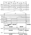
図4を参照して電気光学装置1の動作について説明する。図4は、電気光学装置1における各部の動作を説明するためのタイミングチャートである。
この図に示されるように、走査信号Gwr(1)〜Gwr(m)が順次Lレベルに切り替えられて、1フレーム期間1Fにおいて1〜m行目の走査線12が1水平走査期間(H)毎に順番に走査される。即ち、複数の走査線12のうちの1つを選択してから次の走査線12を選択するまでの期間が水平走査期間となる。この例では、1フレーム期間がm個の水平走査期間から構成される。
1水平走査期間(H)での動作は、各行の画素回路110にわたって共通である。そこで以下については、i行目が水平走査される水平走査期間において、特にi行(3j−2)列の画素回路110について着目して動作を説明する。
<Operation of the first embodiment>
The operation of the electro-
As shown in this figure, the scanning signals Gwr (1) to Gwr (m) are sequentially switched to the L level, and the scanning lines 12 on the 1st to mth lines in the
The operation in one horizontal scanning period (H) is common throughout the
本実施形態ではi行目の走査期間は、大別すると、図4において(b)で示される初期化期間と(c)で示される補償期間と(d)で示される書込期間とに分けられる。そして、(d)の書込期間の後、(a)で示される発光期間となり、1フレームの期間経過後に再びi行目の走査期間に至る。このため、時間の順でいえば、(発光期間)→初期化期間→補償期間→書込期間→(発光期間)というサイクルの繰り返しとなる。
ここで、初期化期間の開始から書込期間の終了までの期間は、選択した走査線12に対応する画素へのデータ書込に関する動作期間である。動作期間は、データを書き込む期間及びデータを書き込むために必要な動作を実行する期間であり、初期化期間、補償期間、及び書込期間は例示である。1水平走査期間(H)は、動作期間と遷移期間とからなる。
そして、本実施形態では、画面全体の輝度を調整するために、制御回路3は、遷移期間においてOLED130の状態を発光又は非発光の一方から他方へ遷移するように制御している。
In the present embodiment, the scanning period of the i-th line is roughly divided into an initialization period shown by (b), a compensation period shown by (c), and a writing period shown by (d) in FIG. Be done. Then, after the writing period of (d), the light emitting period indicated by (a) is reached, and after the period of one frame elapses, the scanning period of the i-th row is reached again. Therefore, in the order of time, the cycle of (light emitting period) → initialization period → compensation period → writing period → (light emitting period) is repeated.
Here, the period from the start of the initialization period to the end of the writing period is an operation period related to data writing to the pixels corresponding to the selected scanning
Then, in the present embodiment, in order to adjust the brightness of the entire screen, the
<発光期間>
説明の便宜上、初期化期間の前提となる発光期間から説明する。図4に示されるように、i行目の発光期間では、走査信号Gwr(i)がHレベルであり、制御信号Gel(i)はLレベルである。また、論理信号である制御信号Gel(i)、Gcmp(i)、Gorst(i)のうち、制御信号Gel(i)がLレベルであり、制御信号Gcmp(i)、Gorst(i)がHレベルである。
このため、図5に示されるようにi行(3j−2)列の画素回路110においては、トランジスター124がオンする一方、トランジスター122、123、125がオフする。したがって、トランジスター121は、ゲート・ソース間の電圧Vgsに応じた電流IdsをOLED130に供給する。後述するように、本実施形態において発光期間での電圧Vgsは、トランジスター121の閾値電圧から、データ信号の電位に応じてレベルシフトした値である。このため、OLED130には、階調レベルに応じた電流がトランジスター121の閾値電圧を補償した状態で供給されることになる。
<Light emission period>
For convenience of explanation, the light emission period, which is the premise of the initialization period, will be described first. As shown in FIG. 4, the scanning signal Gwr (i) is at the H level and the control signal Gel (i) is at the L level during the light emission period of the i-th row. Further, among the control signals Gel (i), Gcmp (i), and Gorst (i), which are logic signals, the control signal Gel (i) is at the L level, and the control signals Gcmp (i) and Gorst (i) are H. It is a level.
Therefore, as shown in FIG. 5, in the
なお、i行目の発光期間は、i行目以外が水平走査される期間であるから、データ線14の電位は適宜変動する。ただし、i行目の画素回路110においては、トランジスター122がオフしているので、ここでは、データ線14の電位変動を考慮していない。
また、図5においては、動作説明で重要となる経路を太線で示している(以下の図6〜図8においても同様である)。
Since the light emitting period of the i-th row is a period during which the other than the i-th row is horizontally scanned, the potential of the
Further, in FIG. 5, the routes that are important in the operation explanation are shown by thick lines (the same applies to FIGS. 6 to 8 below).
<初期化期間>
次にi行目の水平走査期間に至ると、まず、(b)の初期化期間が開始する。初期化期間では、発光期間と比較して、制御信号Gel(i)がHレベルに、制御信号Gorst(i)がLレベルに、それぞれ変化する。
このため、図6に示されるように、i行(3j−2)列の画素回路110においてはトランジスター124がオフし、トランジスター125がオンする。これによってOLED130に供給される電流の経路が遮断されるとともに、OLED130のアノードが電位Vorstにリセットされる。
OLED130は、上述したようにアノードとカソードとで有機EL層を挟持した構成であるので、アノード・カソードの間には、図において破線で示されるように容量Coledが並列に寄生する。発光期間においてOLED130に電流が流れていたときに、当該OLED130のアノード・カソード間の両端電圧が当該容量Coledによって保持されるが、この保持電圧は、トランジスター125のオンによってリセットされる。このため、本実施形態では、後の発光期間においてOLED130に再び電流が流れるときに、当該容量Coledで保持されている電圧の影響を受けにくくなる。
<Initialization period>
Next, when the horizontal scanning period of the i-th row is reached, the initialization period of (b) starts first. In the initialization period, the control signal Gel (i) changes to the H level and the control signal Gorst (i) changes to the L level as compared with the light emission period.
Therefore, as shown in FIG. 6, in the
Since the
詳細には、例えば高輝度の表示状態から低輝度の表示状態に転じるときに、リセットしない構成であると、輝度が高い(大電流が流れた)ときの高電圧が保持されてしまうので、次に、小電流を流そうとしても、過剰な電流が流れてしまって、低輝度の表示状態にさせることができなくなる。これに対して、本実施形態では、トランジスター125のオンによってOLED130のアノードの電位がリセットされるので、低輝度側の再現性が高められることになる。
なお、本実施形態において、電位Vorstについては、当該電位Vorstと共通電極118の電位Vctとの差がOLED130の発光閾値電圧を下回るように設定される。このため、初期化期間(次に説明する補償期間および書込期間)において、OLED130はオフ(非発光)状態である。
In detail, for example, when the display state changes from the high brightness display state to the low brightness display state, if the configuration is not reset, the high voltage when the brightness is high (a large current flows) is maintained. In addition, even if a small current is to be passed, an excessive current will flow, and it will not be possible to obtain a low-luminance display state. On the other hand, in the present embodiment, the potential of the anode of the
In the present embodiment, the potential Vorst is set so that the difference between the potential Vorst and the potential Vct of the
一方、初期化期間では、制御信号/GiniがLレベルになり、制御信号GrefがHレベルになるので、データ転送回路40においては、図6に示されるようにトランジスター45、43がそれぞれオンする。このため、保持容量44の一端であるデータ線14は電位Viniに、保持容量44の他端であるノードhは電位Vrefに、それぞれ初期化される。
On the other hand, in the initialization period, the control signal / Gini becomes the L level and the control signal Gref becomes the H level. Therefore, in the
本実施形態において電位Viniについては、(Vel−Vini)がトランジスター121の閾値電圧|Vth|よりも大きくなるように設定される。なお、トランジスター121はPチャネル型であるので、ソースノードの電位を基準とした閾値電圧Vthは負である。そこで、高低関係の説明で混乱が生じるのを防ぐために、閾値電圧については、絶対値の|Vth|で表し、大小関係で規定することにする。
また、本実施形態において電位Vrefについては、データ信号Vd(1)〜Vd(n)が取り得る電位に対して、後の書込期間においてノードhの電位が上昇変化するような値に、例えば最低値Vminよりも低くなるように設定される。
In the present embodiment, the potential Vini is set so that (Vel-Vini) is larger than the threshold voltage | Vth | of the
Further, in the present embodiment, the potential Vref is set to a value such that the potential of the node h rises and changes in a later writing period with respect to the potential that the data signals Vd (1) to Vd (n) can take. It is set to be lower than the minimum value Vmin.
<補償期間>
i行目の水平走査期間では、次に(c)の補償期間となる。補償期間では初期化期間と比較して、走査信号Gwr(i)および制御信号Gcmp(i)がLレベルとなる。一方、補償期間では、制御信号GrefがHレベルに維持された状態で制御信号/GiniがHレベルになる。
このため、図7に示されるように、データ転送回路40においては、トランジスター43がオンした状態でトランジスター45がオフすることによって、ノードhが電位Vrefに固定される。一方、i行(3j−2)列の画素回路110ではトランジスター122がオンすることによって、ゲートノードgがデータ線14に電気的に接続されるので、補償期間の開始当初においてゲートノードgは電位Viniとなる。
<Compensation period>
In the horizontal scanning period of the i-th row, the compensation period of (c) is next. In the compensation period, the scanning signal Gwr (i) and the control signal Gcmp (i) are at the L level as compared with the initialization period. On the other hand, in the compensation period, the control signal / Gini becomes the H level while the control signal Gref is maintained at the H level.
Therefore, as shown in FIG. 7, in the
補償期間においてトランジスター123がオンするので、トランジスター121はダイオード接続となる。このため、トランジスター121にはドレイン電流が流れて、ゲートノードgおよびデータ線14を充電する。詳細には、電流が、給電線116→トランジスター121→トランジスター123→トランジスター122→(3j−2)列目のデータ線14という経路で流れる。このため、トランジスター121のオンによって互いに接続状態にあるデータ線14およびゲートノードgは、電位Viniから上昇する。
ただし、上記経路に流れる電流は、ゲートノードgが電位(Vel−|Vth|)に近づくにつれて流れにくくなるので、補償期間の終了に至るまでに、データ線14およびゲートノードgは電位(Vel−|Vth|)で飽和する。したがって、保持容量132は、補償期間の終了に至るまでにトランジスター121の閾値電圧|Vth|を保持することになる。
Since the
However, the current flowing in the above path becomes difficult to flow as the gate node g approaches the potential (Vel− | Vth |), so that the
<書込期間>
初期化期間の後、(d)の書込期間に至る。書込期間では、制御信号Gcmp(i)がHレベルになるので、トランジスター121のダイオード接続が解除される一方、制御信号GrefがLレベルになるので、トランジスター43がオフになる。このため、(3j−2)列目のデータ線14からi行(3j−2)列の画素回路110におけるゲートノードgに至るまでの経路はフローティング状態になるものの、当該経路における電位は、保持容量50、132によって(Vel−|Vth|)に維持される。
<Writing period>
After the initialization period, the writing period of (d) is reached. During the writing period, the control signal Gcmp (i) becomes H level, so that the diode connection of the
i行目の書込期間において制御回路3は、j番目のグループでいえば、データ信号Vd(j)を順番に、i行(3j−2)列、i行(3j−1)列、i行(3j)列の画素の階調レベルに応じた電位に切り替える。一方、制御回路3は、データ信号の電位の切り替えに合わせて制御信号Sel(1)、Sel(2)、Sel(3)を順番に排他的にHレベルとする。制御回路3は、図4では省略しているが、制御信号Sel(1)、Sel(2)、Sel(3)とは論理反転の関係にある制御信号/Sel(1)、/Sel(2)、/Sel(3)についても出力している。これによって、デマルチプレクサ30では、各グループにおいてトランスミッションゲート34がそれぞれ左端列、中央列、右端列の順番でオンする。
In the writing period of the i-th row, in the j-th group, the
ここで、左端列のトランスミッションゲート34が制御信号Sel(1)、/Sel(1)によってオンしたとき、図8に示されるように、保持容量44の他端であるノードhは、初期化期間および補償期間において固定された電位Vrefから、データ信号Vd(j)の電位に、すなわちi行(3j−2)列の画素の階調レベルに応じた電位に変化する。このときのノードhの電位変化分をΔVとして、変化後の電位を(Vref+ΔV)として表すことにする。
一方、ゲートノードgは、保持容量44の一端にデータ線14を介して接続されているので、補償期間における電位(Vel−|Vth|)から、ノードhの電位変化分ΔVに容量比k1を乗じた値だけ、上昇方向にシフトした値(Vel−|Vth|+k1・ΔV)となる。このとき、トランジスター121の電圧Vgsで絶対値で表現すると、閾値電圧|Vth|からゲートノードgの電位上昇したシフト分だけ減じた値(|Vth|−k1・ΔV)となる。
なお、容量比k1は、Crf1/(Cdt+Crf1)である。厳密にいえば、保持容量132の容量Cpixも考慮しなければならないが、容量Cpixは、容量Crf1、Cdtに比較して十分に小さくなるように設定しているので、無視している。
Here, when the
On the other hand, since the gate node g is connected to one end of the holding
The capacity ratio k1 is Crf1 / (Cdt + Crf1). Strictly speaking, the capacity Cpix of the holding
i行目の書込期間の終了した後、1水平走査期間が終了すると発光期間に至る。この発光期間では、上述したように制御信号Gel(i)がLレベルになるので、i行(3j−2)列の画素回路110においては、トランジスター124がオンする。ゲート・ソース間の電圧Vgsは、(|Vth|−k1・ΔV)であるから、OLED130には、先の図5に示したように、階調レベルに応じた電流がトランジスター121の閾値電圧を補償した状態で供給されることになる。
このような動作は、i行目の走査期間において、(3j−2)列目の画素回路110以外のi行目の他の画素回路110においても時間的に並列して実行される。さらに、このようなi行目の動作は、実際には、1フレームの期間において1、2、3、…、(m−1)、m行目の順番で実行されるとともに、フレーム毎に繰り返される。
After the end of the writing period of the i-th line, when the one horizontal scanning period ends, the light emitting period is reached. During this light emission period, the control signal Gel (i) becomes the L level as described above, so that the
Such an operation is executed in parallel in time in the
本実施形態によれば、ゲートノードgにおける電位範囲ΔVgateは、データ信号の電位範囲ΔVdataに対し狭められるので、データ信号を細かい精度で刻まなくても、階調レベルを反映した電圧を、トランジスター121のゲート・ソース間に印加することができる。このため、微細な画素回路110においてトランジスター121のゲート・ソース間の電圧Vgsの変化に対しOLED130に流れる微小電流が相対的に大きく変化する場合であっても、OLED130に供給する電流を精度良く制御することが可能になる。
According to the present embodiment, the potential range ΔVgate at the gate node g is narrowed with respect to the potential range ΔVdata of the data signal, so that the voltage reflecting the gradation level can be applied to the
また、図3において破線で示されるようにデータ線14と画素回路110におけるゲートノードgとの間には容量Cprsが実際には寄生する。このため、データ線14の電位変化幅が大きいと、当該容量Cprsを介してゲートノードgに伝播し、いわゆるクロストークやムラなどが発生して表示品位を低下させてしまう。当該容量Cprsの影響は、画素回路110が微細化されたときに顕著に現れる。
これに対して、本実施形態においては、データ線14の電位変化範囲についても、データ信号の電位範囲ΔVdataに対し狭められるので、容量Cprsを介した影響を抑えることができる。
Further, as shown by the broken line in FIG. 3, the capacitance Cprs actually parasitizes between the
On the other hand, in the present embodiment, the potential change range of the
<画面全体の明るさの制御>
次に、電気光学装置1の画面全体の平均輝度の制御について説明する。本実施形態の電気光学装置1は、i行目の走査線12が選択されてから当該i行目の走査線12が次に選択されるまでの期間において、当該i行目の走査線12に接続された画素回路110の発光素子(OLED130)に供給される駆動電流Idsの電流経路に設けられたトランジスター124のオン/オフを繰り返すデューティ制御により、画面全体の平均輝度を調整できるように構成されている。
図9は、i行目の画素回路110についてのデューティ制御を説明するための図であり、同図は走査信号Gwr(i)と制御信号Gel(i)とを模式的に示したものである。デューティ制御は、図11に示すように、制御信号Gel(i)を櫛歯状の波形とし、制御信号Gel(i)がアクティブ(Lレベル)である期間の長さを制御することにより実現される。
<Control of the brightness of the entire screen>
Next, control of the average brightness of the entire screen of the electro-
FIG. 9 is a diagram for explaining duty control for the
デューティ制御による平均輝度の調整態様としては、V同期デューティ制御とH同期デューティ制御の2つの態様が挙げられる。図10は、i番目の行についてのV同期デューティ制御の説明図であり、図11はi番目の行についてのH同期デューティ制御の説明図である。V同期デューティ制御は、図10に示すように、i番目の行が選択されてから当該i番目の行が選択されるまでの1フレーム期間における制御信号Gel(i)のオンパルス数を増減させることで当該i番目の行の画素回路110の平均輝度を調整する態様である。図10の左側に示す制御信号Gel(i)が調整前の状態である。調整前の状態よりも明るくする場合、制御回路3は、図10の右上に示すように制御信号Gel(i)のパルス数を増やすように制御する。一方、調整前の状態よりも暗くする場合、制御回路3は、図10の右下に示すように制御信号Gel(i)のパルス数を減らすように制御する。このように、V同期デューティ制御は、1フレーム期間におけるパルス数で平均輝度を調整する態様であるため、調整能力は走査線12の数に依存する。例えば、走査線12の数が720の場合、パルス数の最小は1、最大は720であり、これが調整範囲および分解能となる。
There are two modes of adjusting the average brightness by duty control: V-synchronous duty control and H-synchronous duty control. FIG. 10 is an explanatory diagram of V-synchronous duty control for the i-th row, and FIG. 11 is an explanatory diagram of H-synchronous duty control for the i-th row. As shown in FIG. 10, the V-synchronous duty control increases or decreases the number of on-pulses of the control signal Gel (i) in one frame period from the selection of the i-th row to the selection of the i-th row. In this embodiment, the average brightness of the
これに対して、H同期デューティ制御は、図11に示すように、1水平走査期間(H)における制御信号Gel(i)のオンパルス幅を増減させることで画素回路110の平均輝度を調整する態様である。図11の左側に示す制御信号Gel(i)が調整前の状態である。調整前の状態よりも明るくする場合、制御回路3は、図11の右上に示すように制御信号Gel(i)のパルス幅を広げるように制御する。一方、調整前の状態よりも暗くする場合、制御回路3は、図11の右下に示すように制御信号Gel(i)のパルス幅を狭めるように制御する。H同期デューティ制御は、1水平走査期間(H)におけるパルス幅で平均輝度を調整する態様であるため、パルスを生成するクロックの周波数によってその調整範囲および分解能が決まる。
On the other hand, in the H synchronous duty control, as shown in FIG. 11, the average brightness of the
ところで、H同期デューティ制御では、1水平走査期間内で、OLED130の状態を発光から非発光、あるいは非発光から発光といったように切り換える。このため、各画素回路110のトランジスター124が同時にオフからオンに遷移することがある。すると、給電線116に大電流が流れ、電源の電位Velが変動してしまう。電源電位の変動が動作期間に発生すると、画素回路110にデータ電圧を正確に書き込むことができず、表示ムラが発生し、表示品質が劣化してしまう。
By the way, in the H synchronous duty control, the state of the
そこで、本実施形態では、OLED130の状態を発光又は非発光の一方から他方へ遷移させる場合、OLED130の状態を図4に示す遷移期間において遷移させている。図4に示す例では、第i行の走査線12が選択されている。この時、第m行の走査線12(非選択)に対応する画素回路110においてトランジスター124を時刻t1においてオフからオンに切り換え、時刻t2においてオンからオフに切り換えている。時刻t1及び時刻t2においては、電源の電位Velが変動するが、初期化、補償、及びデータの書込は実行されないので、第i行のデータの書き込みには影響を与えず、表示品質を向上させることができる。
Therefore, in the present embodiment, when the state of the
また、制御回路3は、V同期デューティ制御において、1フレーム期間を構成する複数の水平走査期間のうち発光素子を発光させる水平走査期間を特定する第1処理を実行する。更に、制御回路3は、H同期デューティ制御において、第1処理によって特定された水平走査期間において、トランジスター124をオンさせる期間を特定する第2処理とを実行する。但し、第2処理において、トランジスター124をオフからオンに遷移させるタイミングとトランジスター124をオンからオフに遷移させるタイミングを、遷移期間中に発生させる。
In addition, the
また、本実施形態において、制御回路3は、画面全体の平均輝度に応じて、第1態様の制御と第2態様の制御を切り換える。第1態様は、動作期間においてトランジスター124をオンさせ、遷移期間においてトランジスター124をオンからオフに切り換えた後にオンに戻す。第2態様は、動作期間においてトランジスター124をオフさせ、遷移期間においてトランジスター124をオフからオンに切り換えた後にオフに戻すものである。
例えば、図4に示す制御信号Gel(1)は、動作期間においてトランジスター124をオンさせ、時刻t1においてトランジスター124をオンからオフに遷移させ、時刻t2において再びオフからオンに遷移させるものである。このため、第1態様の例示となる。第1態様は動作期間を発光に割り当てるので、明るい画像の表示に好適である。第2態様は動作期間を非発光に割り当てるので、暗い画像の表示に好適である。即ち、制御回路3は、画面全体の平均輝度に応じて、第1態様と第2態様とを切り換えることが望ましい。これにより、遷移期間が、仮に、1水平走査期間(H)の半分の時間であっても、平均輝度を0%〜100%の間で調整することが可能となる。
Further, in the present embodiment, the
For example, the control signal Gel (1) shown in FIG. 4 turns on the
上述したように、V同期デューティ制御の調整範囲および分解能を決定する要素(走査線12の数)とH同期デューティ制御の調整範囲および分解能を決定する要素(パルスを生成するクロックの周波数)は互いに独立であるため、V同期デューティ制御とH同期デューティ制御は各々完全に独立して実行可能である。本実施形態の電気光学装置1は、V同期デューティ制御とH同期デューティ制御の両方を実行可能なように構成されている。その理由は以下の通りである。
As described above, the elements that determine the adjustment range and resolution of V-synchronous duty control (the number of scanning lines 12) and the elements that determine the adjustment range and resolution of H-synchronous duty control (the frequency of the clock that generates the pulse) are mutually exclusive. Since they are independent, the V-synchronous duty control and the H-synchronous duty control can be executed completely independently. The electro-
本実施形態における電気光学装置1は、前述したように、ヘッドマウント・ディスプレイにおいて画像を表示に使用されるマイクロ・ディスプレイである。ヘッドマウント・ディスプレイにおいては、左目用の画像を表示するマイクロ・ディスプレイと右目用の画像を表示するマイクロ・ディスプレイとがそれぞれ設けられることが一般的である。このようなヘッドマウント・ディスプレイでは、左目用の画像と右目用の画像の明るさを揃える左右調整と、左右の画像の明るさを一律で明るく或いは暗くする全体調整とをそれぞれ独立に行えることが好ましい。本実施形態の電気光学装置1は左右調整と全体調整をそれぞれ独立に行えるようにするために、上記2種類のデューティ制御を実行可能なように構成されている。例えば、電気光学装置1の制御回路3は、左右調整の実行指示を与えられた場合には、V同期デューティ制御で平均輝度の調整を行い、全体調整の実行指示を与えられた場合にはH同期デューティ制御で平均輝度の調整を行う、といった具合である。なお、本実施形態とは逆に左右調整をH同期デューティ制御で実現し、全体調整を同期デューティ制御で実現しても良い。
As described above, the electro-
左右調整と全体調整のうち、特に左右調整については、表示ユニット(電気光学装置1)〜レンズユニット〜導光ユニットを経た出力光を左右で均一化することが重要である。このため、左右の明るさについては、これら3要素(表示ユニット、レンズユニットおよび導光ユニット)の各々の特性を加味して設定しておく必要がある。この明るさの設定については、ヘッドマウント・ディスプレイの出荷前に計測器で明るさを計測して決定しておいても良いし、左右の出力光を検出する検出素子をヘッドマウント・ディスプレイに設け、この手段による計測結果に応じて決定しておいても良い。 Of the left-right adjustment and the overall adjustment, especially for the left-right adjustment, it is important to make the output light passing through the display unit (electro-optic device 1), the lens unit, and the light guide unit uniform on the left and right. Therefore, it is necessary to set the left and right brightness in consideration of the characteristics of each of these three elements (display unit, lens unit, and light guide unit). This brightness setting may be determined by measuring the brightness with a measuring instrument before shipping the head-mounted display, or the head-mounted display is provided with detection elements for detecting the left and right output lights. , It may be decided according to the measurement result by this means.
本実施形態によれば、選択行の画素回路110について、動作期間に、発光素子がオンからオフまたはオフからオンに切り替えられることはない。このため、本実施形態によれば、OLED130をオンからオフまたはオフからオンへ切り換えることによって電源の電位変動が発生したとしても、データ電圧のずれの発生が回避され、当該データ電圧のずれに起因するムラの発生を回避することができる。つまり、本実施形態によれば、データ信号が供給される素子の発光のオン/オフに起因する電位変動の影響を抑制し、表示品位を向上することができる。なお、Gel調整範囲としてどの程度の時間長の時間区間を確保できるかは、1水平走査期間(H)、初期化期間、補償期間および書き込み期間の各々の時間長に応じて定まるが、1水平走査期間(H)の時間長の40%程度の時間長を確保できれば、画素回路110について0〜100%の平均輝度を確保できると考えられる。
According to the present embodiment, the light emitting element of the
<第2実施形態>
上記第1実施形態では、1水平走査期間(H)のうち、遷移期間において、発光行の発光素子を発光状態から非発光状態へ或いは非発光状態から発光状態へ遷移させることで、選択行におけるデータ書き込みに悪影響が発生することを回避し、表示品位の向上を実現させた。しかし、全ての発光行の発光素子を同じタイミングで発光状態から非発光状態へ或いは非発光状態から発光状態へ遷移させると、大きな電位変動が生じ、次の水平走査期間(H)の選択行における閾値電圧Vthの補償期間の開始までに電源電位が復旧せず、表示品位の低下を招く虞がある。
<Second Embodiment>
In the first embodiment, in the transition period of one horizontal scanning period (H), the light emitting element of the light emitting line is changed from the light emitting state to the non-light emitting state or from the non-light emitting state to the light emitting state in the selected row. The display quality has been improved by avoiding adverse effects on data writing. However, when the light emitting elements of all the light emitting rows are changed from the light emitting state to the non-light emitting state or from the non-light emitting state to the light emitting state at the same timing, a large potential fluctuation occurs, and in the selected row of the next horizontal scanning period (H). The power supply potential may not be restored by the start of the compensation period of the threshold voltage Vth, which may lead to deterioration of display quality.
そこで、本実施形態では、表示部100に含まれる複数の画素回路110を複数のグループにグループ分けし、遷移期間においてグループ毎に発光素子を発光状態から非発光状態へ或いは非発光状態から発光状態へ遷移させるタイミングを異ならせる点を除いて、第1実施形態の電気光学装置1と同様に構成されている。
Therefore, in the present embodiment, the plurality of
図12は、本実施形態による画素回路110のグループ分けの一例を示す図である。図12に示すように、本実施形態では、表示部100に含まれる複数の画素回路110は、列方向にグループ1〜グループ4の4つのグループにグループ分けされている。図13は、各グループに属する画素回路110に与える制御信号Gelの立ち上げおよび立ち下げタイミングの一例を示す図である。図13に示すように、本実施形態では、グループ毎に異なるタイミングで制御信号Gelの立ち上げおよび立ち下げが行われるため、電位変動のピークが分散し、表示品位の低下を回避することができる。
但し、全てのグループで、発光時間と非発光時間との割合は一定となっている。また、トランジスター124がオン又はオフの一方から他方へ遷移するのは、遷移期間に限られており、動作期間では遷移させない。
FIG. 12 is a diagram showing an example of grouping of the
However, the ratio of the light emission time to the non-light emission time is constant in all groups. Further, the transition of the
本実施形態では、表示部100に含まれる複数の画素回路110を4つのグループにグループ分けする場合について説明したが、2または3、或いは5つ以上のグループにグループ分けしても良く、また、グループ内で当該グループに属する画素回路110が列方向に連続して並んでいる必要もない。例えば、2つのグループにグループ分けする態様としては、奇数番目の走査線12に接続された画素回路110のグループと偶数番目の走査線12に接続された画素回路110のグループにグループ分けする態様が考えられる。
In the present embodiment, the case where the plurality of
<変形例>
本発明は、上述した実施形態に限定されるものではなく、例えば次に述べるような各種の変形が可能である。また、次に述べる変形の態様は、任意に選択された一または複数を、適宜に組み合わせることもできる。
<Modification example>
The present invention is not limited to the above-described embodiment, and various modifications such as those described below are possible. Further, in the following modification modes, one or a plurality of arbitrarily selected variants may be appropriately combined.
<変形例1>
上述した第2実施形態では、表示部100に含まれる複数の画素回路110を複数のグループにグループ分けし、グループ毎に遷移期間における制御信号Gelの立ち上或いは立ち下げタイミングを異ならせる場合について説明した。しかし。発光素子の発光/非発光の切り替えに起因する電位変動のピークが十分に分散され、Vth補償やデータ書き込みに悪影響を及ぼさないのであれば、制御信号Gelの立ち上或いは立ち下げタイミングを遷移範囲に限定する必要はない。要は、表示部100に含まれる複数の画素回路110を複数のグループにグループ分けし、グループ毎に発光素子をオンからオフにするタイミングまたはオフからオンにするタイミングが異なっていれば良い。
<Modification example 1>
In the second embodiment described above, a case where a plurality of
<変形例2>
上述した実施形態では、データ線14を3列毎にブロック化するとともに、各ブロックにおいてデータ線14を順番に選択して、データ信号を供給する構成としたが、グループを構成するデータ線数は、「2」以上「3n」以下の所定数であればよい。例えば、グループを構成するデータ線数は、「2」であっても良いし、「4」以上であっても良い。
また、グループ化せずに、すなわちデマルチプレクサ30を用いないで各列のデータ線14にデータ信号を一斉に線順次で供給する構成でも良い。
<
In the above-described embodiment, the data lines 14 are blocked in every three columns, and the data lines 14 are sequentially selected in each block to supply the data signal. However, the number of data lines constituting the group is , A predetermined number of "2" or more and "3n" or less may be used. For example, the number of data lines constituting the group may be "2" or "4" or more.
Further, the data signals may be supplied to the data lines 14 in each column all at once without grouping, that is, without using the
<変形例3>
上述した実施形態では、トランジスター121〜125をPチャネル型で統一したが、Nチャネル型で統一しても良い。また、Pチャネル型及びNチャネル型を適宜組み合わせても良い。
例えば、トランジスター121〜125をNチャネル型で統一する場合、上述した実施形態における、データ信号Vd(n)とは、正負が逆転した電位を、各画素回路110に供給すればよい。また、この場合、トランジスター121〜125のソース及びドレインは、上述した実施形態及び変形例とは逆転した関係となる。
<Modification example 3>
In the above-described embodiment, the
For example, when the
<変形例4>
上述した実施形態及び変形例では、電気光学素子として発光素子であるOLEDを例示したが、例えば無機発光ダイオードやLED(Light Emitting Diode)など、電流に応じた輝度で発光するものであれば良い。
<変形例5>
上述した実施形態及び変形例では、データ転送回路40を用いて、電荷を画素回路110に転送することによって、データを画素回路110に書き込んだが、本発明はこれに限定されるものではない。また、画素回路110は、5個のトランジスター121〜125で構成されたが、本発明はこれに限定されるものではなく、トランジスター123、トランジスター125は適宜省略してもよい。つまり、書込用のトランジスター122、駆動用のトランジスター121、発光制御用のトランジスター124を備えるものであってもよい。
<Modification example 4>
In the above-described embodiment and modification, the OLED which is a light emitting element is exemplified as the electro-optical element, but for example, an inorganic light emitting diode or an LED (Light Emitting Diode) which emits light with a brightness corresponding to a current may be used.
<Modification 5>
In the above-described embodiments and modifications, data is written to the
<応用例>
次に、実施形態等や応用例に係る電気光学装置1を適用した電子機器について説明する。電気光学装置1は、画素が小サイズで高精細な表示な用途に向いている。そこで、電子機器として、ヘッドマウント・ディスプレイを例に挙げて説明する。
<Application example>
Next, an electronic device to which the electro-
図14は、本発明に係る電気光学装置がヘッドマウント・ディスプレイに適用された様子を示す概略図である。図14に示すように、本実施形態のヘッドマウント・ディスプレイ200は、ユーザーの頭部の前方に位置するフロントフレーム210と、フロントフレーム210の両端に接続され頭部の両側方に位置する一対のサイドフレーム220と、フロントフレーム210に固定され眼前を覆う光学パネル250と、それぞれのサイドフレーム220に固定される回路カバー230と、電気光学装置270と、を備える。
FIG. 14 is a schematic view showing how the electro-optical device according to the present invention is applied to a head-mounted display. As shown in FIG. 14, the head-mounted
本実施形態の電気光学装置270は、表示パネルの数が2つとされる。また、制御回路3として、輝度バランス調整入力部51及び全体明るさ調整入力部52を備える点を除いて、第1実施形態の電気光学装置1と同じ構成とされる。
一対の表示パネルDI1,DI2は、光学パネル250内に配置され、表示パネルDI1が左眼の眼前に配置され、表示パネルDI2が右眼の眼前に配置される。これらの表示パネルDI1,DI2から出射する光は光学パネル250から出射される。一方の表示パネルDI1はユーザーの左眼で視認され、他方の表示パネルDI2はユーザーの右眼で視認される。
The electro-
The pair of display panels DI1 and DI2 are arranged in the
また、本実施形態のヘッドマウント・ディスプレイ200では、一方のサイドフレーム2
20に輝度バランス調整入力部51が操作可能に設けられており、他方のサイドフレーム
220に全体明るさ調整入力部52が操作可能に設けられている。輝度バランス調整入力部51は上述したH同期デューティ制御を実行し、全体明るさ調整入力部52は上述したV同期デューティ制御を実行する。また、本実施形態のヘッドマウント・ディスプレイ200では、一方のサイドフレーム220に固定される回路カバー230内に制御回路3が配置され、他方のサイドフレーム220に固定される回路カバー230内に電源回路DCが配置される。ただし、これらの配置は適宜変更可能である。
Further, in the head-mounted
The brightness balance
一般的にヘッドマウント・ディスプレイにおいては、ユーザーにより視認される画像の明るさを変更したいという要求がある。このような要求に対して、本実施形態のヘッドマウント・ディスプレイ200によれば、電気光学装置2の全体明るさを第1実施形態の説明と同様に変更することで、画像の明るさを変更することができる。また、表示パネルDI1、DI2が一対とされ、一方の表示パネルDI1が人の一方の眼から視認され、他方の表示部DI2が人の他方の眼から視認される場合、それぞれの表示パネルDI1,DI2の輝度が異なるとユーザーが違和感を覚える傾向にあり、左右の表示パネルDI1,DI2の輝度の調整を行いたいという要求がある。このような要求に対し、本実施形態のヘッドマウント・ディスプレイ200によれば、電気光学装置270において、第1実施形態での説明と同様にして、左右の表示パネルDI1,DI2間の輝度バランスの調整を行うことができる。そして、上記の画像の明るさの変更と、左右の表示パネルDI1,DI2間の輝度バランスの調整とを独立して行うことができる。
Generally, in a head-mounted display, there is a demand to change the brightness of an image viewed by a user. In response to such a request, according to the head-mounted
図15は、本発明に係る電気光学装置がプロジェクタに適用された様子を示す概略図である。図15に示すようにプロジェクタ300は、筐体350と、電気光学装置370と、ダイクロイックプリズム310と、投影レンズ320とを備える。
FIG. 15 is a schematic view showing how the electro-optical device according to the present invention is applied to a projector. As shown in FIG. 15, the
本実施形態の電気光学装置370は、表示パネルの数が3つとされる。また、制御回路3として、輝度バランス調整入力部51及び全体明るさ調整入力部52を備える点を除いて、第1実施形態の電気光学装置1と同じ構成とされる。
各表示パネルDI1,DI2,DI3は筐体350内に配置され、表示パネルDI1,DI2,DI3の各画素アレイPAは、単色の画素Pを備える。本実施形態では、表示パネルDI1は赤色の画像を表示し、表示パネルDI2は緑色の画像を表示し、表示部DI3は青色の画像を表示する。また、それぞれの表示パネルDI1,DI2,DI3は、互いに隣り合う表示部の光の出射方向が概ね90度となるように配置され、本実施形態では、表示パネルDI1と表示パネルDI2とが隣り合い、表示パネルDI2と表示部DI3
とが隣り合い、表示パネルDI1と表示部DI3とが対向して配置される。
The electro-
Each display panel DI1, DI2, DI3 is arranged in the
Are adjacent to each other, and the display panel DI1 and the display unit DI3 are arranged so as to face each other.
各表示パネルDI1,DI2,DI3に囲まれる位置にはダイクロイックプリズム310が配置され、各表示パネルDI1,DI2,DI3とダイクロイックプリズム310の側面である光入射面とが対向している。また、ダイクロイックプリズム310の光の出射面側には投影レンズ320が配置され、投影レンズ320を介して筐体350の中の光が筐体350の外へ出射することができる。なお、投影レンズ320は、1枚のレンズで構成されても、複数のレンズで構成されても良い。
A
また、筐体350の外側には、輝度バランス調整入力部51及び全体明るさ調整入力部
52が操作可能に設けられている。このプロジェクタ300の使用時において、表示パネルDI1から出射する赤色の光と、表示パネルDI2から出射する緑色の光と、表示パネルDI3から出射する青色の光とが互いに重ね合わされ、赤色の画像と緑色の画像と青色の画像とが重なるカラーの画像が、スクリーン330に映し出される。なお、このスクリーン330は、光透過型であっても、光反射型のスクリーンであっても良い。
Further, on the outside of the
プロジェクタ300の使用に際し、プロジェクタ300を使用する部屋の明るさに応じ
て、プロジェクタ300から出射する光の明るさを変更したいという要求がある。この要
求に対して、本実施形態のプロジェクタ300によれば、電気光学装置370の全体明るさを第1実施形態での説明と同様にして変更することで、プロジェクタ300から出射する光の明るさを変更することができる。また、本実施形態のプロジェクタ300のようにカラー画像を映し出すものにおいては、ホワイトバランスを調整したいという要求がある。この要求に対し、本実施形態のプロジェクタ300によれば、第1実施形態での説明と同様にして、電気光学装置370の3つの表示パネルDI1,DI2,DI3間の輝度バランスを調整することにより、赤、緑、青の輝度バランスを調整でき、ホワイトバランスを調整することができる。そして、プロジェクタ300から出射する光の明るさの変更と、ホワイトバランスの調整とを独立して行うことができる。
When using the
なお、本実施形態では、表示パネルDI1,DI2,DI3として、上述したように赤、緑、青の特定の色のみを発光するものに限定されることなく、他の色を発光するものであっても良い。 In the present embodiment, the display panels DI1, DI2, and DI3 are not limited to those that emit only specific colors of red, green, and blue as described above, but emit other colors. You may.
また、上記実施形態では、各表示パネルDI1,DI2,DI3が赤、緑、青の画像を表示する場合について説明したが、それぞれの各表示パネルDI1,DI2,DI3が画像を表示せず、各表示パネルDI1,DI2,DI3が赤、緑、青の光源となっても良い。この場合、各表示パネルDI1,DI2,DI3の前に液晶パネル等を配置して、当該液晶パネルにより、各表示パネルDI1,DI2,DI3から出射する光に基づいて画像を表示しても良い。 Further, in the above embodiment, the case where each display panel DI1, DI2, DI3 displays a red, green, and blue image has been described, but each display panel DI1, DI2, DI3 does not display an image, and each display panel DI1, DI2, DI3 does not display an image. The display panels DI1, DI2, and DI3 may serve as red, green, and blue light sources. In this case, a liquid crystal panel or the like may be arranged in front of each display panel DI1, DI2, DI3, and the liquid crystal panel may display an image based on the light emitted from each display panel DI1, DI2, DI3.
なお、電気光学装置1については、ヘッドマウント・ディスプレイ200のほかにも、ビデオカメラやレンズ交換式のデジタルカメラなどにおける電子式ビューファインダー、タブレット端末などの携帯情報端末や腕時計、プロジェクタにおける情報表示部にも適用可能である。また、上記実施形態では、ヘッドマウント・ディスプレイにおける左右調整への本発明の適用例を説明した、全体調整をH同期デューティ制御で実現し、この全体調整に本発明を適用しても良い。また、例えば3枚のパネル映像を合成して表示する3板プロジェクタにおける「各パネル調整」(パネル毎の明るさの調整)或いは「全体調整」(3枚のパネル全体での明るさの調整)に本発明を適用しても良い。例えば、「全体調整」をV同期デューティ制御で実現する一方、「各パネル調整」をH同期デューティ制御で実現し、このH同期デューティ制御に本発明を適用する、といった具合である。さらに電気光学装置1を1つだけ含む電子機器における「個体ばらつき調整」或いは「製品使用時の明るさ調整」に本発明を適用しても良い。例えば、「製品使用時の明るさ調整」をV同期デューティ制御で実現する一方、「個体ばらつき調整」をH同期デューティ制御で実現し、このH同期デューティ制御に本発明を適用する、といった具合である。
Regarding the electro-
1、270、370…電気光学装置、10…表示パネル、3…制御回路、5…データ転送線駆動回路、20…走査線駆動回路、12…走査線、14…データ線、16…給電線、30…デマルチプレクサ、70…データ信号供給回路、110…画素回路、116…給電線、121、122,123,124,125…トランジスター、130…OLED、132…保持容量、200…ヘッドマウント・ディスプレイ、300…プロジェクタ。
1,270,370 ... Electro-optical device, 10 ... Display panel, 3 ... Control circuit, 5 ... Data transfer line drive circuit, 20 ... Scan line drive circuit, 12 ... Scan line, 14 ... Data line, 16 ... Feed line, 30 ... Demultiplexer, 70 ... Data signal supply circuit, 110 ... Pixel circuit, 116 ... Power supply line, 121, 122, 123, 124, 125 ... Transistor, 130 ... OLED, 132 ... Holding capacity, 200 ... Head mount display, 300 ... Projector.
Claims (11)
前記発光素子を発光させ又は非発光となるように制御する制御回路とを備え、
前記複数の走査線のうちの1つを選択してから次の走査線を選択するまでの水平走査期間のうち、当該選択した走査線に対応する画素へのデータ書込に関する動作期間を除いた期間を遷移期間としたとき、
前記制御回路は、前記発光素子を発光させる水平走査期間において、当該発光素子を発光させる発光時間と非発光とする非発光時間との割合を制御し、非選択の走査線に対応する画素の発光素子の状態を発光又は非発光の一方から他方へ遷移させる場合、当該発光素子の状態を前記遷移期間において遷移させる、
ことを特徴とする電気光学装置。 A plurality of pixels having a light emitting element, which is arranged corresponding to each intersection position where a plurality of scanning lines and a plurality of data lines intersect and each emits light by a driving current,
It is provided with a control circuit that controls the light emitting element so that it emits light or does not emit light.
Of the horizontal scanning period from the selection of one of the plurality of scanning lines to the selection of the next scanning line, the operation period related to data writing to the pixel corresponding to the selected scanning line was excluded. When the period is the transition period
The control circuit controls the ratio of the light emitting time for causing the light emitting element to emit light and the non-light emitting time for non-light emission during the horizontal scanning period for causing the light emitting element to emit light, and emits light of pixels corresponding to the non-selected scanning lines. When the state of the element is changed from one of light emitting or non-light emitting to the other, the state of the light emitting element is changed in the transition period.
An electro-optical device characterized by this.
前記制御回路は、
前記発光素子を発光させる場合に前記スイッチング素子をオンさせ、前記発光素子を非発光とする場合に前記スイッチング素子をオフさせ、
非選択の走査線に対応する画素の発光素子の状態を発光又は非発光の一方から他方へ遷移させる場合、当該画素のスイッチング素子を前記遷移期間においてオン又はオフの一方から他方へ遷移させる、
請求項1に記載の電気光学装置。 The plurality of pixels have a switching element provided in the current path of the drive current supplied to the light emitting element.
The control circuit
When the light emitting element emits light, the switching element is turned on, and when the light emitting element is not emitted, the switching element is turned off.
When the state of the light emitting element of the pixel corresponding to the non-selective scanning line is changed from one of light emitting or non-light emitting to the other, the switching element of the pixel is changed from one of on or off to the other in the transition period.
The electro-optical device according to claim 1.
前記動作期間において前記スイッチング素子はオン状態であり、前記遷移期間において前記スイッチング素子をオンからオフに切り換えた後にオンに戻す第1態様と、
前記動作期間において前記スイッチング素子をはオフ状態であり、前記遷移期間において前記スイッチング素子をオフからオンに切り換えた後にオフに戻す第2態様と、
を画面全体の平均輝度に応じて切り換える、
請求項2に記載の電気光学装置。 The control circuit
A first aspect in which the switching element is in the ON state during the operation period, and the switching element is switched from on to off during the transition period and then turned back on.
A second aspect in which the switching element is in the off state during the operation period, and the switching element is switched from off to on and then turned off during the transition period .
To switch according to the average brightness of the entire screen,
The electro-optical device according to claim 2.
1フレーム期間を構成する複数の水平走査期間のうち前記発光素子を発光させる水平走査期間を特定する第1処理と、前記第1処理によって特定された水平走査期間において、前記スイッチング素子をオンさせる期間を特定する第2処理とを実行し、
前記第2処理において、前記スイッチング素子をオフからオンに遷移させるタイミングと前記スイッチング素子をオンからオフに遷移させるタイミングを、前記遷移期間中に発生させる、
請求項2または3に記載の電気光学装置。 The control circuit
A first process for specifying the horizontal scanning period for causing the light emitting element to emit light among a plurality of horizontal scanning periods constituting one frame period, and a period for turning on the switching element in the horizontal scanning period specified by the first process. Execute the second process to identify
In the second process, the timing of transitioning the switching element from off to on and the timing of transitioning the switching element from on to off are generated during the transition period.
The electro-optical device according to claim 2 or 3.
前記発光素子を発光させる水平走査期間において、当該発光素子を発光させる発光時間と非発光とする非発光時間との割合を制御し、非選択の走査線に対応する画素の発光素子の状態を発光又は非発光の一方から他方へ遷移させる場合、記複数の画素を複数のグループにグループ分けしたグループ毎に前記スイッチング素子をオン又はオフの一方から他方へ遷移させるタイミングを異ならせる制御回路と、
を備える電気光学装置。 It is arranged corresponding to each intersection position where a plurality of scanning lines and a plurality of data lines intersect, and is provided in a light emitting element in which each emits light by a driving current and a current path for supplying the driving current to the light emitting element. Multiple pixels with switching elements and
In the horizontal scanning period in which the light emitting element emits light, the ratio of the light emitting time for emitting the light emitting element to the non-light emitting time for non-light emission is controlled, and the state of the light emitting element of the pixel corresponding to the non-selected scanning line is emitted. Or, when transitioning from one of the non-emissions to the other, a control circuit that makes the timing of transitioning the switching element from one of the on or off to the other different for each group in which a plurality of pixels are grouped into a plurality of groups.
An electro-optic device.
前記発光素子を発光させ又は非発光となるように制御する制御回路とを備え、 It is provided with a control circuit that controls the light emitting element so that it emits light or does not emit light.
前記m行の走査線のうち、i行目の走査線を選択してから(i+1)行目の走査線を選択するまでの水平走査期間は動作期間と遷移期間とを有し、 Of the m-th row scanning lines, the horizontal scanning period from the selection of the i-th row scanning line to the selection of the (i + 1) -th row scanning line has an operation period and a transition period.
前記制御回路は、 The control circuit
前記動作期間において、前記i行目の走査線を選択し、前記m行の画素のうちi行目の画素へデータを書き込み、前記m行の画素のうちm行目の画素において前記発光素子は発光状態又は非発光状態の一方であり、 In the operation period, the scanning line of the i-th row is selected, data is written to the pixel of the i-th row among the pixels of the m-th row, and the light emitting element is generated in the pixel of the m-th row of the pixels of the m-th row. It is either luminescent or non-luminous,
前記遷移期間において、前記m行目の画素において前記発光素子を発光状態又は非発光状態の一方から他方へ遷移させる、 In the transition period, the light emitting element is transitioned from one of the light emitting state or the non-light emitting state to the other in the pixel on the mth row.
ことを特徴とする電気光学装置。 An electro-optical device characterized by this.
前記遷移期間において、前記m行目の画素において前記発光素子を発光状態又は非発光状態の一方から他方へ遷移させた後、前記発光素子を発光状態又は非発光状態の他方から一方へ遷移させる、 In the transition period, after the light emitting element is transitioned from one of the light emitting state or the non-light emitting state to the other in the pixel on the m-th row, the light emitting element is changed from the other of the light emitting state or the non-light emitting state to one.
請求項6に記載の電気光学装置。 The electro-optical device according to claim 6.
前記遷移期間において、前記m行の画素のうち、前記i行目の画素を除く、2行以上の画素において、前記発光素子を発光状態又は非発光状態の一方から他方へ遷移させる、 In the transition period, the light emitting element is transitioned from one of the light emitting state or the non-light emitting state to the other in two or more rows of the pixels of the m row, excluding the pixel of the i-th row.
請求項6又は請求項7に記載の電気光学装置。 The electro-optical device according to claim 6 or 7.
前記発光素子を発光させ又は非発光となるように制御し、
前記複数の走査線のうちの1つを選択してから次の走査線を選択するまでの水平走査期間のうち、当該選択した走査線に対応する画素へのデータ書込に関する動作期間を除いた期間を遷移期間としたとき、
前記発光素子を発光させる水平走査期間において、当該発光素子を発光させる発光時間と非発光とする非発光時間との割合を制御し、
非選択の走査線に対応する画素の発光素子の状態を発光又は非発光の一方から他方へ遷移させる場合、当該発光素子の状態を前記遷移期間において遷移させる、
ことを特徴とする電気光学装置の駆動方法。 A method for driving an electro-optic device having a plurality of pixels, each of which is arranged corresponding to each intersection position where a plurality of scanning lines and a plurality of data lines intersect and each of which has a light emitting element that emits light by a driving current.
Control the light emitting element so that it emits light or does not emit light,
Of the horizontal scanning period from the selection of one of the plurality of scanning lines to the selection of the next scanning line, the operation period related to data writing to the pixel corresponding to the selected scanning line was excluded. When the period is the transition period
In the horizontal scanning period in which the light emitting element emits light, the ratio of the light emitting time for causing the light emitting element to emit light and the non-light emitting time for non-light emission is controlled.
When the state of the light emitting element of the pixel corresponding to the non-selective scanning line is changed from one of light emitting or non-light emitting to the other, the state of the light emitting element is changed in the transition period.
A method of driving an electro-optic device.
前記発光素子を発光させる水平走査期間において、当該発光素子を発光させる発光時間と非発光とする非発光時間との割合を制御し、
非選択の走査線に対応する画素の発光素子の状態を発光又は非発光の一方から他方へ遷移させる場合、記複数の画素を複数のグループにグループ分けしたグループ毎に前記スイッチング素子をオン又はオフの一方から他方へ遷移させるタイミングを異ならせる、
電気光学装置の駆動方法。 It is arranged corresponding to each intersection position where a plurality of scanning lines and a plurality of data lines intersect, and is provided in a light emitting element in which each emits light by a driving current and a current path for supplying the driving current to the light emitting element. A method of driving an electro-optical device having a plurality of pixels including a switching element.
In the horizontal scanning period in which the light emitting element emits light, the ratio of the light emitting time for causing the light emitting element to emit light and the non-light emitting time for non-light emission is controlled.
When the state of the light emitting element of the pixel corresponding to the non-selected scanning line is changed from one of light emitting or non-light emitting to the other, the switching element is turned on or off for each group in which a plurality of pixels are grouped into a plurality of groups. Different timing of transition from one to the other,
How to drive an electro-optic device.
Priority Applications (2)
| Application Number | Priority Date | Filing Date | Title |
|---|---|---|---|
| JP2016222559A JP6812760B2 (en) | 2016-11-15 | 2016-11-15 | Electro-optics, electronic devices, and how to drive electro-optics |
| US15/813,763 US10665160B2 (en) | 2016-11-15 | 2017-11-15 | Electrooptical device, electronic apparatus, and driving method of electrooptical device |
Applications Claiming Priority (1)
| Application Number | Priority Date | Filing Date | Title |
|---|---|---|---|
| JP2016222559A JP6812760B2 (en) | 2016-11-15 | 2016-11-15 | Electro-optics, electronic devices, and how to drive electro-optics |
Publications (3)
| Publication Number | Publication Date |
|---|---|
| JP2018081178A JP2018081178A (en) | 2018-05-24 |
| JP2018081178A5 JP2018081178A5 (en) | 2019-12-19 |
| JP6812760B2 true JP6812760B2 (en) | 2021-01-13 |
Family
ID=62108017
Family Applications (1)
| Application Number | Title | Priority Date | Filing Date |
|---|---|---|---|
| JP2016222559A Active JP6812760B2 (en) | 2016-11-15 | 2016-11-15 | Electro-optics, electronic devices, and how to drive electro-optics |
Country Status (2)
| Country | Link |
|---|---|
| US (1) | US10665160B2 (en) |
| JP (1) | JP6812760B2 (en) |
Families Citing this family (3)
| Publication number | Priority date | Publication date | Assignee | Title |
|---|---|---|---|---|
| KR20200115766A (en) * | 2019-03-25 | 2020-10-08 | 삼성디스플레이 주식회사 | Display device and driving method of the display device |
| JP7396038B2 (en) * | 2019-12-26 | 2023-12-12 | セイコーエプソン株式会社 | Display devices and electronic equipment |
| US11074854B1 (en) * | 2020-03-09 | 2021-07-27 | Novatek Microelectronics Corp. | Driving device and operation method thereof |
Family Cites Families (29)
| Publication number | Priority date | Publication date | Assignee | Title |
|---|---|---|---|---|
| JP4092857B2 (en) | 1999-06-17 | 2008-05-28 | ソニー株式会社 | Image display device |
| JP4049191B2 (en) | 1999-06-17 | 2008-02-20 | ソニー株式会社 | Image display device |
| JP2003108075A (en) | 2001-09-29 | 2003-04-11 | Toshiba Corp | Display device and its driving method |
| TW574529B (en) | 2001-09-28 | 2004-02-01 | Tokyo Shibaura Electric Co | Organic electro-luminescence display device |
| JP4147872B2 (en) * | 2002-09-09 | 2008-09-10 | 日本電気株式会社 | Liquid crystal display device, driving method thereof, and liquid crystal projector device |
| JP4107071B2 (en) * | 2002-11-29 | 2008-06-25 | セイコーエプソン株式会社 | Electronic circuit, electro-optical device, control method of electro-optical device, and electronic apparatus |
| JP2004191752A (en) | 2002-12-12 | 2004-07-08 | Seiko Epson Corp | Electrooptical device, driving method for electrooptical device, and electronic equipment |
| AU2003289213A1 (en) | 2002-12-19 | 2004-07-14 | Semiconductor Energy Laboratory Co., Ltd. | Driving method for light emitting device, and electronic equipment |
| JP2004325940A (en) * | 2003-04-25 | 2004-11-18 | Toshiba Matsushita Display Technology Co Ltd | Active matrix type display device and its driving method |
| JP3882796B2 (en) * | 2003-07-22 | 2007-02-21 | セイコーエプソン株式会社 | Electro-optical device, driving method of electro-optical device, and electronic apparatus |
| JP4071189B2 (en) * | 2003-11-28 | 2008-04-02 | シャープ株式会社 | Signal circuit, display device using the same, and data line driving method |
| JP2006030516A (en) | 2004-07-15 | 2006-02-02 | Sony Corp | Display device and driving method thereof |
| CN100592368C (en) * | 2004-07-21 | 2010-02-24 | 夏普株式会社 | Active matrix type display device and drive control circuit used in the same |
| JP4752331B2 (en) | 2005-05-25 | 2011-08-17 | セイコーエプソン株式会社 | Light emitting device, driving method and driving circuit thereof, and electronic apparatus |
| JP2008026395A (en) * | 2006-07-18 | 2008-02-07 | Sony Corp | Power consumption detection device and method, power consumption controller, image processor, self-luminous light emitting display device, electronic equipment, power consumption control method, and computer program |
| JP5082319B2 (en) * | 2006-07-25 | 2012-11-28 | ソニー株式会社 | Light emission condition control device, image processing device, self light emission display device, electronic device, light emission condition control method, and computer program |
| JP2008083680A (en) * | 2006-08-17 | 2008-04-10 | Seiko Epson Corp | Electro-optical device and electronic apparatus |
| JP2008089956A (en) * | 2006-10-02 | 2008-04-17 | Sony Corp | Power consumption information calculating device, power consumption controller, image processor, spontaneous light emitting display device, electronic apparatus, power consumption information calculating method, power consumption control method, and computer program |
| JP4984863B2 (en) * | 2006-12-08 | 2012-07-25 | ソニー株式会社 | Display device and driving method thereof |
| JP5361139B2 (en) * | 2007-03-09 | 2013-12-04 | キヤノン株式会社 | Display device |
| JP5638181B2 (en) * | 2007-11-09 | 2014-12-10 | セイコーエプソン株式会社 | Driving device and method, electro-optical device, and electronic apparatus |
| JP2009168849A (en) * | 2008-01-10 | 2009-07-30 | Seiko Epson Corp | Electro-optical device, method of driving electro-optical device, and electronic apparatus |
| JP2009204931A (en) * | 2008-02-28 | 2009-09-10 | Sony Corp | El display panel, electronic device, and drive method of el display panel |
| JP2011028135A (en) * | 2009-07-29 | 2011-02-10 | Canon Inc | Display device and driving method of the same |
| JP6064313B2 (en) * | 2011-10-18 | 2017-01-25 | セイコーエプソン株式会社 | Electro-optical device, driving method of electro-optical device, and electronic apparatus |
| JP2015079173A (en) * | 2013-10-18 | 2015-04-23 | セイコーエプソン株式会社 | Electro-optical device, driving method of the same, and electronic apparatus |
| WO2015063981A1 (en) * | 2013-10-30 | 2015-05-07 | 株式会社Joled | Method for interrupting power supply of display apparatus, and display apparatus |
| CN104658475B (en) * | 2013-11-21 | 2017-04-26 | 乐金显示有限公司 | Organic light emitting diode display device |
| JP6535441B2 (en) | 2014-08-06 | 2019-06-26 | セイコーエプソン株式会社 | Electro-optical device, electronic apparatus, and method of driving electro-optical device |
-
2016
- 2016-11-15 JP JP2016222559A patent/JP6812760B2/en active Active
-
2017
- 2017-11-15 US US15/813,763 patent/US10665160B2/en active Active
Also Published As
| Publication number | Publication date |
|---|---|
| US10665160B2 (en) | 2020-05-26 |
| US20180137820A1 (en) | 2018-05-17 |
| JP2018081178A (en) | 2018-05-24 |
Similar Documents
| Publication | Publication Date | Title |
|---|---|---|
| US10186204B2 (en) | Electro-optical device and electronic apparatus | |
| US20180357957A1 (en) | Electro-optical device, electronic apparatus, and method of driving electro-optical device | |
| JP6064313B2 (en) | Electro-optical device, driving method of electro-optical device, and electronic apparatus | |
| JP6911406B2 (en) | Pixel circuits, electro-optics and electronic devices | |
| US10283052B2 (en) | Electro-optical device and electronic apparatus | |
| JP2013088610A (en) | Electro-optic device, electro-optic device driving method and electronic apparatus | |
| JP6492447B2 (en) | Electro-optical device, electronic apparatus, and driving method of electro-optical device | |
| JP6812760B2 (en) | Electro-optics, electronic devices, and how to drive electro-optics | |
| US10964260B2 (en) | Electro-optical device, driving method for electro-optical device, and electronic apparatus | |
| US10417963B2 (en) | Electro-optical apparatus, electronic apparatus, and method for driving electro-optical apparatus | |
| JP2013044847A (en) | Electro-optical device, driving method of electro-optical device and electronic apparatus | |
| US10854142B2 (en) | Display device and electronic apparatus | |
| CN107016958B (en) | Electro-optical device and method for controlling electro-optical device | |
| US11749183B2 (en) | Electro-optical device and electronic apparatus | |
| JP6702352B2 (en) | Electro-optical device and electronic equipment | |
| JP2013088638A (en) | Electro-optical device and electronic apparatus | |
| JP2016212444A (en) | Electro-optic device driving method | |
| JP2015232738A (en) | Electro-optic device and electronic apparatus | |
| JP2021173793A (en) | Display and electronic apparatus | |
| JP2013088640A (en) | Electro-optic device driving method, electro-optic device and electronic apparatus | |
| JP2019008325A (en) | Electro-optic device and electronic apparatus | |
| JP2015004907A (en) | Electro-optic device, method for driving electro-optic device, and electronic equipment |
Legal Events
| Date | Code | Title | Description |
|---|---|---|---|
| A521 | Written amendment |
Free format text: JAPANESE INTERMEDIATE CODE: A523 Effective date: 20191105 |
|
| A621 | Written request for application examination |
Free format text: JAPANESE INTERMEDIATE CODE: A621 Effective date: 20191105 |
|
| A977 | Report on retrieval |
Free format text: JAPANESE INTERMEDIATE CODE: A971007 Effective date: 20201105 |
|
| TRDD | Decision of grant or rejection written | ||
| A01 | Written decision to grant a patent or to grant a registration (utility model) |
Free format text: JAPANESE INTERMEDIATE CODE: A01 Effective date: 20201117 |
|
| A61 | First payment of annual fees (during grant procedure) |
Free format text: JAPANESE INTERMEDIATE CODE: A61 Effective date: 20201130 |
|
| R150 | Certificate of patent or registration of utility model |
Ref document number: 6812760 Country of ref document: JP Free format text: JAPANESE INTERMEDIATE CODE: R150 |