JP6811715B2 - Light emitting element package and lighting equipment - Google Patents
Light emitting element package and lighting equipment Download PDFInfo
- Publication number
- JP6811715B2 JP6811715B2 JP2017543339A JP2017543339A JP6811715B2 JP 6811715 B2 JP6811715 B2 JP 6811715B2 JP 2017543339 A JP2017543339 A JP 2017543339A JP 2017543339 A JP2017543339 A JP 2017543339A JP 6811715 B2 JP6811715 B2 JP 6811715B2
- Authority
- JP
- Japan
- Prior art keywords
- light emitting
- layer
- semiconductor layer
- conductive semiconductor
- segment
- Prior art date
- Legal status (The legal status is an assumption and is not a legal conclusion. Google has not performed a legal analysis and makes no representation as to the accuracy of the status listed.)
- Active
Links
- 239000004065 semiconductor Substances 0.000 claims description 138
- 239000000758 substrate Substances 0.000 claims description 26
- 239000004642 Polyimide Substances 0.000 claims description 11
- 229920001721 polyimide Polymers 0.000 claims description 11
- 239000010410 layer Substances 0.000 description 290
- 239000000126 substance Substances 0.000 description 28
- 229910004298 SiO 2 Inorganic materials 0.000 description 14
- 238000000034 method Methods 0.000 description 14
- PXHVJJICTQNCMI-UHFFFAOYSA-N nickel Substances [Ni] PXHVJJICTQNCMI-UHFFFAOYSA-N 0.000 description 13
- 230000003287 optical effect Effects 0.000 description 13
- 229910000679 solder Inorganic materials 0.000 description 13
- 239000002019 doping agent Substances 0.000 description 12
- 230000008569 process Effects 0.000 description 11
- 229910052782 aluminium Inorganic materials 0.000 description 10
- 239000010931 gold Substances 0.000 description 9
- 239000000463 material Substances 0.000 description 9
- 229910052709 silver Inorganic materials 0.000 description 9
- OAICVXFJPJFONN-UHFFFAOYSA-N Phosphorus Chemical compound [P] OAICVXFJPJFONN-UHFFFAOYSA-N 0.000 description 8
- 239000010936 titanium Substances 0.000 description 8
- 230000004888 barrier function Effects 0.000 description 7
- 150000001875 compounds Chemical class 0.000 description 7
- 238000004519 manufacturing process Methods 0.000 description 7
- 229910052751 metal Inorganic materials 0.000 description 7
- 239000002184 metal Substances 0.000 description 7
- 229910052759 nickel Inorganic materials 0.000 description 7
- BASFCYQUMIYNBI-UHFFFAOYSA-N platinum Substances [Pt] BASFCYQUMIYNBI-UHFFFAOYSA-N 0.000 description 7
- 229910052710 silicon Inorganic materials 0.000 description 7
- 229910002704 AlGaN Inorganic materials 0.000 description 6
- XLOMVQKBTHCTTD-UHFFFAOYSA-N Zinc monoxide Chemical compound [Zn]=O XLOMVQKBTHCTTD-UHFFFAOYSA-N 0.000 description 6
- 229910052791 calcium Inorganic materials 0.000 description 6
- 239000011651 chromium Substances 0.000 description 6
- 230000000052 comparative effect Effects 0.000 description 6
- 239000010948 rhodium Substances 0.000 description 6
- 230000007480 spreading Effects 0.000 description 6
- 238000003892 spreading Methods 0.000 description 6
- 229910052712 strontium Inorganic materials 0.000 description 6
- BQCADISMDOOEFD-UHFFFAOYSA-N Silver Chemical compound [Ag] BQCADISMDOOEFD-UHFFFAOYSA-N 0.000 description 5
- 150000004767 nitrides Chemical class 0.000 description 5
- 229910052697 platinum Inorganic materials 0.000 description 5
- 229910052703 rhodium Inorganic materials 0.000 description 5
- 239000004332 silver Substances 0.000 description 5
- 229910052719 titanium Inorganic materials 0.000 description 5
- 229910052725 zinc Inorganic materials 0.000 description 5
- 239000011701 zinc Substances 0.000 description 5
- 229910000980 Aluminium gallium arsenide Inorganic materials 0.000 description 4
- 229910001218 Gallium arsenide Inorganic materials 0.000 description 4
- 229910052788 barium Inorganic materials 0.000 description 4
- 230000000903 blocking effect Effects 0.000 description 4
- 229910052804 chromium Inorganic materials 0.000 description 4
- 229910052733 gallium Inorganic materials 0.000 description 4
- 229910052737 gold Inorganic materials 0.000 description 4
- VRIVJOXICYMTAG-IYEMJOQQSA-L iron(ii) gluconate Chemical compound [Fe+2].OC[C@@H](O)[C@@H](O)[C@H](O)[C@@H](O)C([O-])=O.OC[C@@H](O)[C@@H](O)[C@H](O)[C@@H](O)C([O-])=O VRIVJOXICYMTAG-IYEMJOQQSA-L 0.000 description 4
- 239000000203 mixture Substances 0.000 description 4
- 229920002120 photoresistant polymer Polymers 0.000 description 4
- 239000002096 quantum dot Substances 0.000 description 4
- 239000010944 silver (metal) Substances 0.000 description 4
- 239000011135 tin Substances 0.000 description 4
- 229910018072 Al 2 O 3 Inorganic materials 0.000 description 3
- UCKMPCXJQFINFW-UHFFFAOYSA-N Sulphide Chemical compound [S-2] UCKMPCXJQFINFW-UHFFFAOYSA-N 0.000 description 3
- 229910010413 TiO 2 Inorganic materials 0.000 description 3
- GEIAQOFPUVMAGM-UHFFFAOYSA-N ZrO Inorganic materials [Zr]=O GEIAQOFPUVMAGM-UHFFFAOYSA-N 0.000 description 3
- 239000000969 carrier Substances 0.000 description 3
- 239000011810 insulating material Substances 0.000 description 3
- 229910052741 iridium Inorganic materials 0.000 description 3
- 229910052749 magnesium Inorganic materials 0.000 description 3
- 238000000465 moulding Methods 0.000 description 3
- 229910052760 oxygen Inorganic materials 0.000 description 3
- 229910052763 palladium Inorganic materials 0.000 description 3
- KDLHZDBZIXYQEI-UHFFFAOYSA-N palladium Substances [Pd] KDLHZDBZIXYQEI-UHFFFAOYSA-N 0.000 description 3
- 229910052594 sapphire Inorganic materials 0.000 description 3
- 239000010980 sapphire Substances 0.000 description 3
- 229910052718 tin Inorganic materials 0.000 description 3
- YVTHLONGBIQYBO-UHFFFAOYSA-N zinc indium(3+) oxygen(2-) Chemical compound [O--].[Zn++].[In+3] YVTHLONGBIQYBO-UHFFFAOYSA-N 0.000 description 3
- 239000011787 zinc oxide Substances 0.000 description 3
- BPQQTUXANYXVAA-UHFFFAOYSA-N Orthosilicate Chemical compound [O-][Si]([O-])([O-])[O-] BPQQTUXANYXVAA-UHFFFAOYSA-N 0.000 description 2
- 229910019897 RuOx Inorganic materials 0.000 description 2
- XUIMIQQOPSSXEZ-UHFFFAOYSA-N Silicon Chemical compound [Si] XUIMIQQOPSSXEZ-UHFFFAOYSA-N 0.000 description 2
- 229910052771 Terbium Inorganic materials 0.000 description 2
- 230000002411 adverse Effects 0.000 description 2
- 238000000151 deposition Methods 0.000 description 2
- JAONJTDQXUSBGG-UHFFFAOYSA-N dialuminum;dizinc;oxygen(2-) Chemical compound [O-2].[O-2].[O-2].[O-2].[O-2].[Al+3].[Al+3].[Zn+2].[Zn+2] JAONJTDQXUSBGG-UHFFFAOYSA-N 0.000 description 2
- 229910052732 germanium Inorganic materials 0.000 description 2
- 239000012535 impurity Substances 0.000 description 2
- 229910052738 indium Inorganic materials 0.000 description 2
- 239000007769 metal material Substances 0.000 description 2
- 230000005012 migration Effects 0.000 description 2
- 238000013508 migration Methods 0.000 description 2
- 238000012986 modification Methods 0.000 description 2
- 230000004048 modification Effects 0.000 description 2
- 229910052757 nitrogen Inorganic materials 0.000 description 2
- 229910052711 selenium Inorganic materials 0.000 description 2
- 239000010703 silicon Substances 0.000 description 2
- SKRWFPLZQAAQSU-UHFFFAOYSA-N stibanylidynetin;hydrate Chemical compound O.[Sn].[Sb] SKRWFPLZQAAQSU-UHFFFAOYSA-N 0.000 description 2
- 229910052714 tellurium Inorganic materials 0.000 description 2
- IUVCFHHAEHNCFT-INIZCTEOSA-N 2-[(1s)-1-[4-amino-3-(3-fluoro-4-propan-2-yloxyphenyl)pyrazolo[3,4-d]pyrimidin-1-yl]ethyl]-6-fluoro-3-(3-fluorophenyl)chromen-4-one Chemical compound C1=C(F)C(OC(C)C)=CC=C1C(C1=C(N)N=CN=C11)=NN1[C@@H](C)C1=C(C=2C=C(F)C=CC=2)C(=O)C2=CC(F)=CC=C2O1 IUVCFHHAEHNCFT-INIZCTEOSA-N 0.000 description 1
- VYZAMTAEIAYCRO-UHFFFAOYSA-N Chromium Chemical compound [Cr] VYZAMTAEIAYCRO-UHFFFAOYSA-N 0.000 description 1
- 229910052691 Erbium Inorganic materials 0.000 description 1
- 229910052693 Europium Inorganic materials 0.000 description 1
- 229910052688 Gadolinium Inorganic materials 0.000 description 1
- GYHNNYVSQQEPJS-UHFFFAOYSA-N Gallium Chemical compound [Ga] GYHNNYVSQQEPJS-UHFFFAOYSA-N 0.000 description 1
- 229910052765 Lutetium Inorganic materials 0.000 description 1
- 229910052772 Samarium Inorganic materials 0.000 description 1
- 229910003564 SiAlON Inorganic materials 0.000 description 1
- RTAQQCXQSZGOHL-UHFFFAOYSA-N Titanium Chemical compound [Ti] RTAQQCXQSZGOHL-UHFFFAOYSA-N 0.000 description 1
- 229910052769 Ytterbium Inorganic materials 0.000 description 1
- DZLPZFLXRVRDAE-UHFFFAOYSA-N [O--].[O--].[O--].[O--].[Al+3].[Zn++].[In+3] Chemical compound [O--].[O--].[O--].[O--].[Al+3].[Zn++].[In+3] DZLPZFLXRVRDAE-UHFFFAOYSA-N 0.000 description 1
- 229910045601 alloy Inorganic materials 0.000 description 1
- 239000000956 alloy Substances 0.000 description 1
- XAGFODPZIPBFFR-UHFFFAOYSA-N aluminium Chemical compound [Al] XAGFODPZIPBFFR-UHFFFAOYSA-N 0.000 description 1
- 238000006243 chemical reaction Methods 0.000 description 1
- 239000011162 core material Substances 0.000 description 1
- 230000007547 defect Effects 0.000 description 1
- 230000002950 deficient Effects 0.000 description 1
- 230000008021 deposition Effects 0.000 description 1
- 238000009792 diffusion process Methods 0.000 description 1
- 238000002845 discoloration Methods 0.000 description 1
- 238000009826 distribution Methods 0.000 description 1
- 230000005611 electricity Effects 0.000 description 1
- PCHJSUWPFVWCPO-UHFFFAOYSA-N gold Chemical compound [Au] PCHJSUWPFVWCPO-UHFFFAOYSA-N 0.000 description 1
- 230000006872 improvement Effects 0.000 description 1
- AMGQUBHHOARCQH-UHFFFAOYSA-N indium;oxotin Chemical compound [In].[Sn]=O AMGQUBHHOARCQH-UHFFFAOYSA-N 0.000 description 1
- 238000009413 insulation Methods 0.000 description 1
- 229910052742 iron Inorganic materials 0.000 description 1
- 229910052746 lanthanum Inorganic materials 0.000 description 1
- 235000012054 meals Nutrition 0.000 description 1
- QSHDDOUJBYECFT-UHFFFAOYSA-N mercury Chemical compound [Hg] QSHDDOUJBYECFT-UHFFFAOYSA-N 0.000 description 1
- 229910052753 mercury Inorganic materials 0.000 description 1
- 239000002245 particle Substances 0.000 description 1
- 238000005192 partition Methods 0.000 description 1
- 230000035515 penetration Effects 0.000 description 1
- MHOVAHRLVXNVSD-UHFFFAOYSA-N rhodium atom Chemical compound [Rh] MHOVAHRLVXNVSD-UHFFFAOYSA-N 0.000 description 1
- 229910052706 scandium Inorganic materials 0.000 description 1
- 239000002356 single layer Substances 0.000 description 1
- 229910052717 sulfur Inorganic materials 0.000 description 1
- 239000000057 synthetic resin Substances 0.000 description 1
- 229920003002 synthetic resin Polymers 0.000 description 1
- XOLBLPGZBRYERU-UHFFFAOYSA-N tin dioxide Chemical compound O=[Sn]=O XOLBLPGZBRYERU-UHFFFAOYSA-N 0.000 description 1
- 229910001887 tin oxide Inorganic materials 0.000 description 1
- 230000007704 transition Effects 0.000 description 1
- 229910052727 yttrium Inorganic materials 0.000 description 1
Images


Classifications
-
- H—ELECTRICITY
- H01—ELECTRIC ELEMENTS
- H01L—SEMICONDUCTOR DEVICES NOT COVERED BY CLASS H10
- H01L33/00—Semiconductor devices with at least one potential-jump barrier or surface barrier specially adapted for light emission; Processes or apparatus specially adapted for the manufacture or treatment thereof or of parts thereof; Details thereof
- H01L33/02—Semiconductor devices with at least one potential-jump barrier or surface barrier specially adapted for light emission; Processes or apparatus specially adapted for the manufacture or treatment thereof or of parts thereof; Details thereof characterised by the semiconductor bodies
- H01L33/14—Semiconductor devices with at least one potential-jump barrier or surface barrier specially adapted for light emission; Processes or apparatus specially adapted for the manufacture or treatment thereof or of parts thereof; Details thereof characterised by the semiconductor bodies with a carrier transport control structure, e.g. highly-doped semiconductor layer or current-blocking structure
-
- H—ELECTRICITY
- H01—ELECTRIC ELEMENTS
- H01L—SEMICONDUCTOR DEVICES NOT COVERED BY CLASS H10
- H01L33/00—Semiconductor devices with at least one potential-jump barrier or surface barrier specially adapted for light emission; Processes or apparatus specially adapted for the manufacture or treatment thereof or of parts thereof; Details thereof
- H01L33/44—Semiconductor devices with at least one potential-jump barrier or surface barrier specially adapted for light emission; Processes or apparatus specially adapted for the manufacture or treatment thereof or of parts thereof; Details thereof characterised by the coatings, e.g. passivation layer or anti-reflective coating
-
- H—ELECTRICITY
- H01—ELECTRIC ELEMENTS
- H01L—SEMICONDUCTOR DEVICES NOT COVERED BY CLASS H10
- H01L33/00—Semiconductor devices with at least one potential-jump barrier or surface barrier specially adapted for light emission; Processes or apparatus specially adapted for the manufacture or treatment thereof or of parts thereof; Details thereof
- H01L33/36—Semiconductor devices with at least one potential-jump barrier or surface barrier specially adapted for light emission; Processes or apparatus specially adapted for the manufacture or treatment thereof or of parts thereof; Details thereof characterised by the electrodes
- H01L33/38—Semiconductor devices with at least one potential-jump barrier or surface barrier specially adapted for light emission; Processes or apparatus specially adapted for the manufacture or treatment thereof or of parts thereof; Details thereof characterised by the electrodes with a particular shape
- H01L33/382—Semiconductor devices with at least one potential-jump barrier or surface barrier specially adapted for light emission; Processes or apparatus specially adapted for the manufacture or treatment thereof or of parts thereof; Details thereof characterised by the electrodes with a particular shape the electrode extending partially in or entirely through the semiconductor body
-
- H—ELECTRICITY
- H01—ELECTRIC ELEMENTS
- H01L—SEMICONDUCTOR DEVICES NOT COVERED BY CLASS H10
- H01L33/00—Semiconductor devices with at least one potential-jump barrier or surface barrier specially adapted for light emission; Processes or apparatus specially adapted for the manufacture or treatment thereof or of parts thereof; Details thereof
- H01L33/48—Semiconductor devices with at least one potential-jump barrier or surface barrier specially adapted for light emission; Processes or apparatus specially adapted for the manufacture or treatment thereof or of parts thereof; Details thereof characterised by the semiconductor body packages
- H01L33/62—Arrangements for conducting electric current to or from the semiconductor body, e.g. lead-frames, wire-bonds or solder balls
-
- H—ELECTRICITY
- H01—ELECTRIC ELEMENTS
- H01L—SEMICONDUCTOR DEVICES NOT COVERED BY CLASS H10
- H01L33/00—Semiconductor devices with at least one potential-jump barrier or surface barrier specially adapted for light emission; Processes or apparatus specially adapted for the manufacture or treatment thereof or of parts thereof; Details thereof
- H01L33/02—Semiconductor devices with at least one potential-jump barrier or surface barrier specially adapted for light emission; Processes or apparatus specially adapted for the manufacture or treatment thereof or of parts thereof; Details thereof characterised by the semiconductor bodies
- H01L33/14—Semiconductor devices with at least one potential-jump barrier or surface barrier specially adapted for light emission; Processes or apparatus specially adapted for the manufacture or treatment thereof or of parts thereof; Details thereof characterised by the semiconductor bodies with a carrier transport control structure, e.g. highly-doped semiconductor layer or current-blocking structure
- H01L33/145—Semiconductor devices with at least one potential-jump barrier or surface barrier specially adapted for light emission; Processes or apparatus specially adapted for the manufacture or treatment thereof or of parts thereof; Details thereof characterised by the semiconductor bodies with a carrier transport control structure, e.g. highly-doped semiconductor layer or current-blocking structure with a current-blocking structure
-
- H—ELECTRICITY
- H01—ELECTRIC ELEMENTS
- H01L—SEMICONDUCTOR DEVICES NOT COVERED BY CLASS H10
- H01L33/00—Semiconductor devices with at least one potential-jump barrier or surface barrier specially adapted for light emission; Processes or apparatus specially adapted for the manufacture or treatment thereof or of parts thereof; Details thereof
- H01L33/02—Semiconductor devices with at least one potential-jump barrier or surface barrier specially adapted for light emission; Processes or apparatus specially adapted for the manufacture or treatment thereof or of parts thereof; Details thereof characterised by the semiconductor bodies
- H01L33/26—Materials of the light emitting region
- H01L33/30—Materials of the light emitting region containing only elements of group III and group V of the periodic system
- H01L33/32—Materials of the light emitting region containing only elements of group III and group V of the periodic system containing nitrogen
-
- H—ELECTRICITY
- H01—ELECTRIC ELEMENTS
- H01L—SEMICONDUCTOR DEVICES NOT COVERED BY CLASS H10
- H01L33/00—Semiconductor devices with at least one potential-jump barrier or surface barrier specially adapted for light emission; Processes or apparatus specially adapted for the manufacture or treatment thereof or of parts thereof; Details thereof
- H01L33/36—Semiconductor devices with at least one potential-jump barrier or surface barrier specially adapted for light emission; Processes or apparatus specially adapted for the manufacture or treatment thereof or of parts thereof; Details thereof characterised by the electrodes
- H01L33/40—Materials therefor
- H01L33/405—Reflective materials
Description
実施例は発光素子パッケージ及び照明装置に関するものである。 Examples relate to light emitting device packages and lighting devices.
発光ダイオード(LED:Light Emitting Diode)は化合物半導体の特性を用いて電気を赤外線又は光に変換させて信号をやり取りするとか、光源として使われる半導体素子の一種である。 A light emitting diode (LED: Light Emitting Diode) is a type of semiconductor element used as a light source, such as converting electricity into infrared rays or light to exchange signals by using the characteristics of a compound semiconductor.
III−V族窒化物半導体(group III−V nitride semiconductor)は物理的及び化学的特性によって発光ダイオード(LED)又はレーザーダイオード(LD:Laser Diode)などの発光素子の核心素材として脚光を浴びている。 Group III-V nitride semiconductors are in the limelight as the core material of light emitting elements such as light emitting diodes (LEDs) or laser diodes (LDs) due to their physical and chemical properties. ..
このような発光ダイオードは白熱灯と蛍光灯などの既存の照明器具に使われる水銀(Hg)のような環境有害物質を含んでいなくて環境に非常に優しく、長い寿命と低電力消費特性などの利点があるので、既存の光源を取り替えている。 Such light emitting diodes are extremely environmentally friendly because they do not contain environmentally harmful substances such as mercury (Hg) used in existing lighting fixtures such as incandescent lamps and fluorescent lamps, and have long life and low power consumption characteristics. The existing light source is being replaced because of the advantages of.
既存の発光素子パッケージの場合、活性層に供給されるキャリアが均等に注入されなくて電流スプレッディングが悪化することがあるため、その改善が要求される。 In the case of the existing light emitting device package, the carriers supplied to the active layer may not be evenly injected and the current spreading may deteriorate, so improvement is required.
実施例は電流スプレッディングが改善し、簡単で迅速に製造可能な発光素子パッケージ及び照明装置を提供する。 The embodiment provides a light emitting device package and lighting device with improved current spreading and easy and rapid manufacturing.
一実施例による発光素子パッケージは、基板;前記基板の下側に配置され、第1導電型半導体層、活性層及び第2導電型半導体層を含む発光構造物;前記活性層と前記第2導電型半導体層を貫いて前記第1導電型半導体層を露出させる貫通ホールに埋め込まれ、前記第1導電型半導体層と連結された第1ボンディングパッド;前記第1ボンディングパッドから離隔して前記第2導電型半導体層の下側に配置され、前記第2導電型半導体層と連結された第2ボンディングパッド;前記貫通ホールにおいて前記発光構造物の側部及び前記発光構造物の内側下部縁部に配置された第1絶縁層;及び前記貫通ホールにおいて前記第1絶縁層と前記第1ボンディングパッドの間に配置された第2絶縁層を含むことができる。 The light emitting element package according to one embodiment is a substrate; a light emitting structure arranged under the substrate and including a first conductive semiconductor layer, an active layer and a second conductive semiconductor layer; the active layer and the second conductive layer. A first bonding pad embedded in a through hole that penetrates the mold semiconductor layer and exposes the first conductive semiconductor layer and connected to the first conductive semiconductor layer; the second bonding pad separated from the first bonding pad. A second bonding pad arranged below the conductive semiconductor layer and connected to the second conductive semiconductor layer; arranged at the side portion of the light emitting structure and the inner lower edge portion of the light emitting structure in the through hole. The first insulating layer formed; and the second insulating layer arranged between the first insulating layer and the first bonding pad in the through hole can be included.
例えば、前記第1絶縁層は、貫通ホールにおいて前記発光構造物の側部に配置された第1セグメント;及び前記第1セグメントから前記発光構造物の厚さ方向と交差する第1方向に延びて前記発光構造物の前記内側下部縁部に配置された第2セグメントを含むことができる。前記第1絶縁層は、活性層の下側で前記第1セグメントから前記第1方向に前記第2導電型半導体層の内部に延びて配置された少なくとも一つの第3セグメントをさらに含むことができる。前記第1絶縁層は、発光構造物の外側部及び外側下部縁部にそれぞれ配置された第4セグメントをさらに含むことができる。 For example, the first insulating layer extends from the first segment arranged on the side of the light emitting structure in the through hole; and in the first direction intersecting the thickness direction of the light emitting structure from the first segment. A second segment located at the inner lower edge of the light emitting structure can be included. The first insulating layer may further include at least one third segment which is arranged below the active layer so as to extend from the first segment to the inside of the second conductive semiconductor layer in the first direction. .. The first insulating layer may further include fourth segments arranged on the outer side and the outer lower edge of the light emitting structure, respectively.
例えば、前記発光素子パッケージは、前記貫通ホールから露出された前記第1導電型半導体層と前記第1ボンディングパッドの間に配置された第1電極をさらに含むことができる。前記第2絶縁層は前記第1電極と前記第1絶縁層の間まで延びて配置できる。 For example, the light emitting device package may further include a first electrode arranged between the first conductive semiconductor layer exposed from the through hole and the first bonding pad. The second insulating layer can be arranged so as to extend between the first electrode and the first insulating layer.
例えば、前記発光素子パッケージは、前記第2導電型半導体層と前記第2ボンディングパッドの間に配置された第2電極をさらに含むことができる。 For example, the light emitting device package can further include a second electrode arranged between the second conductive semiconductor layer and the second bonding pad.
例えば、前記第2電極は、前記第2導電型半導体層の下側に配置された反射層;及び前記反射層と前記第2導電型半導体層の間に配置された透光電極層を含むことができる。前記第1絶縁層の前記第2セグメントは前記透光電極層と前記第2導電型半導体層の前記内側下部縁部の間に配置され、前記第4セグメントは前記透光電極層と前記外側下部縁部の間に配置できる。 For example, the second electrode includes a reflective layer arranged below the second conductive semiconductor layer; and a translucent electrode layer arranged between the reflective layer and the second conductive semiconductor layer. Can be done. The second segment of the first insulating layer is arranged between the translucent electrode layer and the inner lower edge portion of the second conductive semiconductor layer, and the fourth segment is the translucent electrode layer and the outer lower portion. Can be placed between the edges.
例えば、前記第2電極は、前記第2導電型半導体層の下側に配置された反射層を含むことができる。前記第1絶縁層の前記第2セグメントは前記反射層と前記第2導電型半導体層の前記内側下部縁部に配置され、前記第4セグメントは前記反射層と前記外側下部縁部の間に配置できる。 For example, the second electrode may include a reflective layer arranged below the second conductive semiconductor layer. The second segment of the first insulating layer is arranged at the inner lower edge portion of the reflective layer and the second conductive semiconductor layer, and the fourth segment is arranged between the reflective layer and the outer lower edge portion. it can.
例えば、前記第2電極は、前記第2導電型半導体層の下側に配置された透光電極層を含むことができる。前記第1絶縁層の前記第2セグメントは前記透光電極層と前記第2導電型半導体層の前記内側下部縁部の間に配置され、前記第4セグメントは前記透光電極層と前記外側下部縁部の間に配置できる。 For example, the second electrode may include a translucent electrode layer arranged below the second conductive semiconductor layer. The second segment of the first insulating layer is arranged between the translucent electrode layer and the inner lower edge portion of the second conductive semiconductor layer, and the fourth segment is the translucent electrode layer and the outer lower portion. Can be placed between the edges.
例えば、前記第3セグメントが配置される前記第2導電型半導体層の内部は、前記第2導電型半導体層の上部、下部又は中間部の中で少なくとも一つを含むことができる。前記少なくとも一つの第3セグメントは、前記第1セグメントから互いに平行に離隔して第1方向に延びた複数の第3セグメントを含むことができる。第2又は第4セグメントの前記第1方向への長さは20μm〜30μmであってもよい。前記第1ボンディングパッドと前記第2ボンディングパッドの前記第1方向への幅の比率は9:1又は8:2であってもよい。前記第1又は第2絶縁層の中で少なくとも一つは感光性ポリイミドを含むことができる。 For example, the inside of the second conductive semiconductor layer on which the third segment is arranged may include at least one in the upper portion, the lower portion, or the intermediate portion of the second conductive semiconductor layer. The at least one third segment can include a plurality of third segments that are separated from each other in parallel with each other and extend in the first direction. The length of the second or fourth segment in the first direction may be 20 μm to 30 μm. The ratio of the width of the first bonding pad to the width of the second bonding pad in the first direction may be 9: 1 or 8: 2. At least one of the first or second insulating layers can contain photosensitive polyimide.
例えば、前記発光素子パッケージは、前記第1及び第2ボンディングパッドとそれぞれ連結された第1及び第2リードフレームをさらに含むことができる。 For example, the light emitting device package can further include first and second lead frames connected to the first and second bonding pads, respectively.
他の実施例による照明装置は、前記発光素子パッケージを含むことができる。 The lighting device according to another embodiment can include the light emitting element package.
実施例による発光素子パッケージ及び照明装置は、電流スプレッディングが弱い部分にキャリアを円滑に注入することができ、高い電流密度及び改善した電流スプレッディングを有し、感光性ポリイミドで第1絶縁層を形成することにより、第1絶縁層としてSiO2を使うときの不良率を解消することができ、製造工程が簡素化して工程時間を短縮することができ、電流遮断層の役目を一層充実に行うことができ、第1絶縁層を提供することにより、第2電極が銀(Ag)でなる反射層を含む場合、銀のマイグレーション又は不純物から発光構造物を保護することができる。 The light emitting device package and the lighting device according to the embodiment can smoothly inject carriers into the portion where the current spreading is weak, have a high current density and improved current spreading, and have a first insulating layer made of photosensitive polyimide. By forming it, the defect rate when SiO 2 is used as the first insulating layer can be eliminated, the manufacturing process can be simplified and the process time can be shortened, and the role of the current blocking layer can be further enhanced. By providing the first insulating layer, the light emitting structure can be protected from silver migration or impurities when the second electrode contains a reflective layer made of silver (Ag).
以下、本発明を具体的に説明するために実施例に基づいて説明し、発明の理解を助けるために添付図面を参照して詳細に説明する。しかし、本発明による実施例は色々の多様な形態に変形可能であり、本発明の範囲が以降で詳述する実施例に限定されるものとして解釈されてはいけない。本発明の実施例は当該業界で平均的な知識を有する者に本発明をより完全に説明するために提供するものである。 Hereinafter, the present invention will be described in detail based on examples in order to specifically explain the present invention, and will be described in detail with reference to the accompanying drawings in order to assist the understanding of the invention. However, the examples according to the present invention can be transformed into various forms and should not be construed as limiting the scope of the present invention to the examples detailed below. The embodiments of the present invention are provided to explain the present invention more completely to a person having average knowledge in the industry.
本発明による実施例の説明において、各要素の“上”又は“下(on or under)”に形成されるものとして記載する場合、上又は下(on or under)は二つの要素が互いに直接(directly)接触するとかあるいは一つ以上の他の要素が前記二つの要素を挟んで(indirectly)形成されるものを全て含む。また、“上”又は“下(on or under)”と表現される場合、一つの要素を基準に上方だけではなく下方の意味も含むことができる。 In the description of the examples according to the present invention, when described as being formed "on or under" of each element, the upper or lower (on or under) means that the two elements are directly attached to each other (on or under). Dilectly) Includes all those that are in contact with each other or in which one or more other elements are formed by sandwiching the two elements. Also, when expressed as "upper" or "lower", it can include not only the upper meaning but also the lower meaning based on one element.
また、以下で用いる“第1”及び“第2”、“上/上部/上方”及び“下/下部/下方”などの関係的用語は、そのような実体又は要素間のどんな物理的又は論理的関係又は手順を必ず要求するとか内包するとかしないながらも、ある一つの実体又は要素を他の実体又は要素と区別するために用いることもできる。 Also, as used below, related terms such as "first" and "second", "upper / upper / upper" and "lower / lower / lower" are any physical or logic between such entities or elements. It can also be used to distinguish one entity or element from another, although it does not necessarily require or include a relationship or procedure.
図面において、各層の厚さや大きさは説明の便宜性及び明確性のために省略するとかあるいは概略的に図示するとかした。また、各構成要素の大きさは実際の大きさをそのまま反映するものではない。 In the drawings, the thickness and size of each layer are omitted or outlined for convenience and clarity of explanation. Moreover, the size of each component does not directly reflect the actual size.
以下、実施例による発光素子パッケージ100、200を添付図面を参照して次のように説明する。便宜上、デカルト座標系(x軸、y軸、z軸)を用いて発光素子パッケージ100、200を説明するが、他の座標系によってもこれを説明することができるのはいうまでもない。デカルト座標系によれば、x軸、y軸及びz軸は互いに直交するが、実施例はこれに限られない。すなわち、他の実施例によると、x軸、y軸及びz軸は互いに交差することもできる。 Hereinafter, the light emitting element packages 100 and 200 according to the examples will be described as follows with reference to the accompanying drawings. For convenience, the Cartesian coordinate system (x-axis, y-axis, z-axis) will be used to describe the light emitting element packages 100 and 200, but it goes without saying that this can also be explained by other coordinate systems. According to the Cartesian coordinate system, the x-axis, y-axis and z-axis are orthogonal to each other, but the examples are not limited to this. That is, according to other embodiments, the x-axis, y-axis and z-axis can also intersect each other.
図1は一実施例による発光素子パッケージ100の平面図を示し、図2は図1に示した発光素子パッケージ100をI−I’線に沿って切開した断面図を示す。
FIG. 1 shows a plan view of the light emitting
理解を助けるため、図1で、第1ボンディングパッド132で覆われる第1貫通ホールTH1を点線で表記し、第1貫通ホールTH1を拡大した図面では第1貫通ホールTH1を実線で表記した。また、図1の場合、第1貫通ホールTH1の個数は16個であるものとして例示しているが、実施例はこれに限られない。すなわち、第1貫通ホールTH1の個数は16個より多くてもよく少なくてもよい。
To aid understanding, in FIG. 1, the first through hole TH1 covered with the
また、図1で、第1貫通ホールTH1は平面円形を有するものとして示しているが、実施例はこれに限られない。すなわち、他の実施例によると、第1貫通ホールTH1は多様な平面形状を有することができる。 Further, in FIG. 1, the first through hole TH1 is shown as having a planar circle, but the embodiment is not limited to this. That is, according to another embodiment, the first through hole TH1 can have various planar shapes.
図1及び図2を参照すると、実施例による発光素子パッケージ100は、基板110、発光構造物120、第1及び第2ボンディングパッド(bonding pad)132、134、第1絶縁層142A、第2絶縁層150及び第1及び第2電極162、164Aを含むことができる。
Referring to FIGS. 1 and 2, the light emitting
基板110の下側に発光構造物120が配置できる。
The
基板110は導電型物質又は非導電型物質を含むことができる。例えば、基板110は、サファイア(Al203)、GaN、SiC、ZnO、GaP、InP、Ga203、GaAs又はSiの中で少なくとも一つを含むことができる。また、活性層124から放出された光が発光素子パッケージ100から脱出することを助けることができるように、例えば基板110はパターン112を有するPSS(Patterned Sapphire Substrate)であってもよいが、実施例はこれに限られない。
The
基板110と発光構造物120間の熱膨張係数の差及び格子不整合を改善するために、これら110、120の間にバッファー層(又は、転移層)(図示せず)が配置できる。バッファー層は、例えばAl、In、N及びGaからなる群から選択される少なくとも1種の物質を含むことができるが、これに限られない。また、バッファー層は単層又は多層の構造を有することもできる。
A buffer layer (or transition layer) (not shown) can be arranged between the
発光構造物120は基板110の下側に配置され、基板110の側に順次積層された第1導電型半導体層122、活性層124及び第2導電型半導体層126を含むことができる。
The
第1導電型半導体層122は基板110の下側に配置され、第1導電型ドーパントがドープされたIII−V族又はII−VI族などの化合物半導体で具現可能である。第1導電型半導体層122がn型半導体層の場合、第1導電型ドーパントはn型ドーパントであり、Si、Ge、Sn、Se及びTeを含むことができるが、これに限定されない。
The first
例えば、第1導電型半導体層122は、AlxInyGa(1−x−y)N(0≦x≦1、0≦y≦1、0≦x+y≦1)の組成式を有する半導体物質を含むことができる。第1導電型半導体層122は、GaN、InN、AlN、InGaN、AlGaN、InAlGaN、AlInN、AlGaAs、InGaAs、AlInGaAs、GaP、AlGaP、InGaP、AlInGaP及びInPの中でいずれか1種以上を含むことができる。
For example, the first
活性層124は第1導電型半導体層122と第2導電型半導体層126の間に配置され、第1導電型半導体層122を通じて注入される電子(又は、正孔)と第2導電型半導体層126を通じて注入される正孔(又は、電子)が互いに会って、活性層124を成す物質固有のエネルギーバンドによって決定されるエネルギーを有する光を放出する層である。活性層124は単一井戸構造、多重井戸構造、単一量子井戸構造、多重量子井戸構造(MQW:Multi Quantum Well)、量子細線(Quantum−Wire)構造、又は量子ドット(Quantum Dot)構造の中で少なくともどの一構造に形成できる。
The
活性層124の井戸層/障壁層は、InGaN/GaN、InGaN/InGaN、GaN/AlGaN、InAlGaN/GaN、GaAs(InGaAs)/AlGaAs、GaP(InGaP)/AlGaPの中でいずれか一つ以上のペア構造に形成できるが、これに限定されない。井戸層は障壁層のバンドギャップエネルギーより低いバンドギャップエネルギーを有する物質で形成できる。
The well layer / barrier layer of the
活性層124の上側又は/及び下側には導電型クラッド層(図示せず)が形成されることもできる。導電型クラッド層は活性層124の障壁層のバンドギャップエネルギーより高いバンドギャップエネルギーを有する半導体で形成できる。例えば、導電型クラッド層はGaN、AlGaN、InAlGaN又は超格子構造などを含むことができる。また、導電型クラッド層はn型又はp型でドープされることができる。
A conductive clad layer (not shown) may be formed on the upper side and / or the lower side of the
第2導電型半導体層126は活性層124の下側に配置され、半導体化合物で形成でき、III−V族又はII−VI族などの化合物半導体で具現可能である。例えば、第2導電型半導体層126はInxAlyGa1−x−yN(0≦x≦1、0≦y≦1、0≦x+y≦1)の組成式を有する半導体物質を含むことができる。第2導電型半導体層126には第2導電型ドーパントがドープされることができる。第2導電型半導体層126がp型半導体層の場合、第2導電型ドーパントはp型ドーパントであり、Mg、Zn、Ca、Sr、Baなどを含むことができる。
The second
第1導電型半導体層122はn型半導体層で、かつ第2導電型半導体層126はp型半導体層で具現することができる。若しくは、第1導電型半導体層122はp型半導体層で、かつ第2導電型半導体層126はn型半導体層で具現することもできる。
The first
発光構造物120はn−p接合構造、p−n接合構造、n−p−n接合構造及びp−n−p接合構造の中でいずれか一構造に具現することができる。
The
以下、説明の便宜上、y軸方向を‘第1方向’といい、発光構造物120の厚さ方向であるx軸方向を‘第2方向’といい、z軸方向を‘第3方向’という。以下、第1、第2及び第3方向は互いに直交すると説明するが、これは第1、第2及び第3方向が互いに交差する場合にも適用可能であるのはいうまでもない。
Hereinafter, for convenience of explanation, the y-axis direction is referred to as the'first direction', the x-axis direction which is the thickness direction of the
第1ボンディングパッド132は第2導電型半導体層126と活性層124を貫いて第1導電型半導体層122を露出させる第1貫通ホールTH1に埋め込まれ、第1電極162を介して第1導電型半導体層122と電気的に連結されることができる。第1ボンディングパッド132は第2方向と直交する第1又は第3方向の中で少なくとも一方向に第1幅W1を有してもよい。図2の場合、第1方向への第1幅W1を示している。
The
第2ボンディングパッド134は第1ボンディングパッド132と第1方向に離隔第2導電型半導体層126の下側に配置され、第2電極164Aを通じて第2導電型半導体層126と電気的に連結されることができる。第2ボンディングパッド134は第2方向と直交する第1又は第3方向の中で少なくとも一方向に第2幅W2を有することができる。図2の場合、第1方向への第2幅W2を示している。
The
第1及び第2ボンディングパッド132、134のそれぞれは電気的伝導性を有する金属物質を含むことができ、第1及び第2電極162、164Aのそれぞれの物質と同じとか違う物質を含むことができる。第1及び第2ボンディングパッド132、134のそれぞれはTi、Ni、Au又はSnの中で少なくとも1種を含むことができるが、実施例はこれに限られない。例えば、第1及び第2ボンディングパッド132、134のそれぞれはTi/Ni/Au/Sn/Auであってもよい。
Each of the first and
また、実施例によると、第1ボンディングパッド132の第1幅W1と第2ボンディングパッド134の第2幅W2の比率は次の式1又は式2のように表現することができるが、実施例はこれに限られない。
Further, according to the embodiment, the ratio of the first width W1 of the
![]()
![]()
![]()
![]()
図3は図2に示した‘A’部に対する一実施例A1の拡大断面図を示す。図3に示した第2電極164Bは図2に示した第2電極164Aと違う構造を有する。これを除けば、図3に示した発光素子パッケージは図2に示した発光素子パッケージと同一である。したがって、図2に示した発光素子パッケージ100の説明において、図3に示した拡大断面図A1を引用する。
FIG. 3 shows an enlarged cross-sectional view of Example A1 with respect to the ‘A’ part shown in FIG. The
図3を参照すると、第1絶縁層142Aは第1貫通ホールTH1において発光構造物120の側部120−1及び発光構造物120の内側下部縁部120−2に配置できる。すなわち、第1絶縁層142Aは第1及び第2セグメントS1、S2を含むことができる。
Referring to FIG. 3, the first insulating
第1セグメントS1は第1貫通ホールTH1において発光構造物120の側部120−1に配置できる。第2セグメントS2は第1セグメントS1から発光構造物120の厚さ方向である第2方向に垂直した第1又は第3方向の中で少なくとも一方向に延び、発光構造物120の内側下部縁部120−2に配置できる。図3の場合、第2セグメントS2は第1セグメントS1から第1方向に延びることを示している。たとえ図示されてはいないが、第2セグメントS2は第1セグメントS1から第3方向に延びることができるのはいうまでもない。
The first segment S1 can be arranged on the side portion 120-1 of the
図4は図2に示した‘A’部に対する他の実施例A2の拡大断面図を示す。図4に示した第2電極164Bは図2に示した第2電極164Aとは違う構造を有し、図4に示した第1絶縁層142Bは図2に示した第1絶縁層142Aとは違う構造を有する。これを除けば、図4に示した発光素子パッケージは図2に示した発光素子パッケージと同一である。したがって、図4で、図2に示した発光素子パッケージ100と同じ部分については重複説明を省略する。
FIG. 4 shows an enlarged cross-sectional view of another Example A2 with respect to the ‘A’ part shown in FIG. The
図4を参照すると、第1絶縁層142Aは第1及び第2セグメントS1、S2だけでなく第3セグメントS3をさらに含むことができる。第3セグメントS3は活性層124の下側で第1セグメントS1から第1方向又は第3方向の中で少なくとも一方向に延びて配置できる。図4の場合、第3セグメントS3が第1セグメントS1から第1方向に延びた形態を示す。たとえ図示されてはいないが、第3セグメントS3は第1セグメントS1から第3方向に延びることができるのはいうまでもない。
Referring to FIG. 4, the first insulating
また、第1絶縁層142Bの第3セグメントS3は第2方向において第2導電型半導体層126の中間部分(又は、中間部)に配置できるが、実施例はこれに限られない。
Further, the third segment S3 of the first insulating
他の実施例によると、第1絶縁層142Bの第3セグメントS3は第2導電型半導体層126の下部に配置されることもできる。この場合、図4に示した第1絶縁層142Bの第3セグメントS3の底面S3−1と第2導電型半導体層126の底面126A間の間隔dは‘0’であってもよい。
According to another embodiment, the third segment S3 of the first insulating
さらに他の実施例によると、第1絶縁層142Bの第3セグメントS3は第2導電型半導体層126の上部にも配置できる。すなわち、第3セグメントS3は第2導電型半導体層126と活性層124の間に配置できる。この場合、第3セグメントS3は活性層124と接して配置できる。
According to still another embodiment, the third segment S3 of the first insulating
また、第1絶縁層142Bの第3セグメントS3は第2導電型半導体層126の上部、中間部分又は下部の中で少なくとも複数箇所に配置された複数の第3セグメントを含むこともできる。例えば、図4に例示したように、第3セグメントS3は複数の第3−1及び第3−2セグメントS3−1、S3−2を含むこともできる。第3−1セグメントS3−1は第2導電型半導体層126の上部で活性層124と第3−2セグメントS3−2の間に配置できる。第3−2セグメントS3−2は第2導電型半導体層126の中間部分で第3−1セグメントS3−1と第2セグメントS2の間に配置できる。
Further, the third segment S3 of the first insulating
また、第1絶縁層142Aは第4セグメントS4をさらに含むことができる。図3を参照すると、第4セグメントS4は発光構造物120の外側部120−3に配置された第4−1セグメントS4−1と発光構造物120の外側下部縁部120−4に配置された第4−2セグメントS4−2を含むこともできる。
Further, the first insulating
前述した第1絶縁層142A、142Bは一種の電流遮断層(CBL:Current Blocking Layer)の役目をすることができる。これについては添付の図6を参照して詳細に後述する。
The first insulating
一方、第2絶縁層150は第1貫通ホールTH1において第1絶縁層142A、142Bと第1ボンディングパッド132の間に配置できる。また、第2絶縁層150は第2電極164A、164Bと第1ボンディングパッド132の間に配置され、第2電極164A、164Bと第1ボンディングパッド132を電気的に絶縁させることができる。
On the other hand, the second insulating
第1絶縁層142A、142B又は第2絶縁層150の中で少なくとも一つは感光性ポリイミド(PSPI:Photo Sensitive Polyimid)で具現できるが、実施例はこれに限られない。若しくは、第1絶縁層142A、142B又は第2絶縁層150の中で少なくとも一つはSiO2、TiO2、ZrO2、Si3N4、Al2O3、又はMgF2の中で少なくとも1種を含むことができる。第1絶縁層142A、142Bと第2絶縁層150は互いに同一又は違う材質を有することができる。
At least one of the first insulating
第1電極162は第1貫通ホールTH1を通じて露出された第1導電型半導体層122と第1ボンディングパッド132の間に配置できる。この場合、第2絶縁層150は第1電極162と第1絶縁層142A、142Bの間に配置できるが、実施例はこれに限られない。
The
第1電極162はオーム接触する物質を含んでオームの役目を行うことによって、別個のオーム層(図示せず)が配置される必要がないこともあり、別個のオーム層が第1電極162と第1導電型半導体層122の間に配置されることもできる。
Since the
第2電極164A、164Bは第2導電型半導体層126と第2ボンディングパッド134の間に配置できる。
The
第1電極162及び第2電極164A、164Bのそれぞれは活性層124から放出された光を吸収せずに反射させるとか透過させることができ、第1及び第2導電型半導体層122、126上に良質で成長可能などの物質でも形成できる。例えば、第1電極162及び第2電極164A、164Bのそれぞれは金属で形成でき、Ag、Ni、Ti、Al、Rh、Pd、Ir、Ru、Mg、Zn、Pt、Au、Hf、Cr及びこれらの選択的な組合せでなることができる。例えば、第1電極162はCr/Ni/Auであってもよいが、実施例はこれに限られない。
Each of the
一実施例によると、図2に示した第2電極164Aは反射層に相当することができる。すなわち、第2電極164Aは、第2導電型半導体層126の下側に配置されて第2導電型半導体層126と電気的に連結される反射層のみを含むことができる。この場合、第1絶縁層142Aの第2セグメントS2は第2電極164Aである反射層と第2導電型半導体層126の内側下部縁部120−2の間に配置できる。ここで、内側下部縁部120−2は図2に図示されてはいないが、図3に示した位置と同一である。また、第1絶縁層142Aの第4−2セグメントS4−2は第2電極164Aである反射層と第2導電型半導体層126の外側下部縁部120−4の間に配置できる。
According to one embodiment, the
第2電極164Aである反射層は、アルミニウム(Al)、金(Au)、銀(Ag)、ニッケル(Ni)、白金(Pt)、ロジウム(Rh)、チタン(Ti)、クロム(Cr)あるいはAl又はAg又はPt又はRhを含む合金を含む金属層でなることができる。例えば、反射層はAg/Ni/Tiであってもよいが、実施例はこれに限られない。
The reflective layer of the
他の実施例によると、図2に示した第2電極164Aは透光電極層に相当することができる。すなわち、第2電極164Aは第2導電型半導体層126の下側に配置された透光電極層のみを含むことができる。この場合、第1絶縁層142Aの第2セグメントS2は第2電極164Aである透光電極層と第2導電型半導体層126の内側下部縁部120−2の間に配置され、第1絶縁層142Aの第4−2セグメントS4−2は第2電極164Aである透光電極層と第2導電型半導体層126の外側下部縁部120−4の間に配置できる。
According to another embodiment, the
図2に示した第2電極164Aである透光電極層は透明伝導性酸化膜(TCO:Tranparent Conductive Oxide)であってもよい。例えば、透光電極層は、ITO(indium tin oxide)、IZO(indium zinc oxide)、IZTO(indium zinc tin oxide)、IAZO(indium aluminum zinc oxide)、IGZO(indium gallium zinc oxide)、IGTO(indium gallium tin oxide)、AZO(aluminum zinc oxide)、ATO(antimony tin oxide)、GZO(gallium zinc oxide)、IrOx、RuOx、RuOx/ITO、Ni/IrOx/Au、及びNi/IrOx/Au/ITOの中で少なくとも1種を含むことができ、このような材料に限定しない。
The translucent electrode layer, which is the
さらに他の実施例によると、図3及び図4に示したように、第2電極164Bは透光電極層164−1及び反射層164−2を全て含むこともできる。
According to still another embodiment, as shown in FIGS. 3 and 4, the
反射層164−2は第2導電型半導体層126の下側に配置され、透光電極層164−1は反射層164−2と第2導電型半導体層126の間に配置できる。この場合、第1絶縁層142Aの第2セグメントS2は透光電極層164−1と第2導電型半導体層126の内側下部縁部120−2の間に配置できる。また、第4−2セグメントS4−2は透光電極層164−1と第2導電型半導体層126の外側下部縁部120−4の間に配置できる。
The reflective layer 164-2 is arranged below the second
また、図3に示した第2電極164Bの場合、透光電極層164−1の第3幅W3より反射層164−2の第4幅W4が小さい。この場合、透光電極層164−1の少なくとも一部が第2方向に第1絶縁層142Aと垂直に重畳する反面、反射層164−2は第2方向に第1絶縁層142Aと垂直に重畳しないこともできる。
Further, in the case of the
図4に示した第2電極164Bの場合、透光電極層164−1の第3幅W3と反射層164−2の第4幅W4は同一である。この場合、透光電極層164−1と反射層164−2のそれぞれの少なくとも一部は第2方向に第1絶縁層142Bと重畳してもよい。
In the case of the
図2〜図4に示した発光素子パッケージ100はフリップチップボンディング構造であるため、活性層124から放出された光は基板110及び第1導電型半導体層122を通じて出射される。このために、基板110及び第1導電型半導体層122は透光性を有する物質でなり、第2導電型半導体層126と第2電極164A、164Bは透光性又は非透光性を有する物質でなることができる。
Since the light emitting
以下、図2に示した発光素子パッケージ100の製造方法を添付の図5a〜図5gを参照して次のように説明するが、実施例はこれに限られない。すなわち、図2に示した発光素子パッケージ100は他の方法によっても製造されることができるのはいうまでもない。また、図3及び図4に示した発光素子パッケージA1、A2の場合にも図5a〜図5gに示した製造方法を変更して製造することができるのは当業者に自明である。また、説明の便宜上、図2に示した発光素子パッケージ100において‘A’部に対する製造方法を図5a〜図5gに基づいて説明するが、‘A’部以外の部分に対する製造過程も図5a〜図5gに示したようである。
Hereinafter, the method for manufacturing the light emitting
図5a〜図5gは図2に示した発光素子パッケージ100の‘A’部の工程断面図を示す。
5a to 5g show a process cross-sectional view of the ‘A’ part of the light emitting
図5aを参照すると、基板110上に発光構造物120を形成する。基板110は導電型物質又は非導電型物質を含むことができる。例えば、基板110はサファイア(Al203)、GaN、SiC、ZnO、GaP、InP、Ga203、GaAs及びSiの中で少なくとも1種を含むことができる。
With reference to FIG. 5a, the
基板110上に第1導電型半導体層122、活性層124及び第2導電型半導体層126を順次積層して発光構造物120を形成することができる。
The
まず、基板110上に第1導電型半導体層122を形成する。第1導電型半導体層122は第1導電型ドーパントがドープされたIII−V族又はII−VI族などの化合物半導体で形成することができる。第1導電型半導体層122がn型半導体層の場合、第1導電型ドーパントはn型ドーパントであり、Si、Ge、Sn、Se、Teを含むことができるが、これに限定されない。
First, the first
例えば、第1導電型半導体層122はAlxInyGa(1−x−y)N(0≦x≦1、0≦y≦1、0≦x+y≦1)の組成式を有する半導体物質を含むことができる。第1導電型半導体層122は、GaN、InN、AlN、InGaN、AlGaN、InAlGaN、AlInN、AlGaAs、InGaAs、AlInGaAs、GaP、AlGaP、InGaP、AlInGaP及びInPの中でいずれか1種以上を含むことができる。
For example, the first
その後、活性層124を第1導電型半導体層122上に形成する。活性層124は単一井戸構造、多重井戸構造、単一量子井戸構造、多重量子井戸構造(MQW:Multi Quantum Well)、量子細線(Quantum−Wire)構造、又は量子ドット(Quantum Dot)構造の中で少なくとも一構造に形成できる。
After that, the
活性層124の井戸層/障壁層は、InGaN/GaN、InGaN/InGaN、GaN/AlGaN、InAlGaN/GaN、GaAs(InGaAs)/AlGaAs、GaP(InGaP)/AlGaPの中でいずれか一ペア以上の構造に形成できるが、これに限定されない。井戸層は障壁層のバンドギャップエネルギーより低いバンドギャップエネルギーを有する物質で形成できる。
The well layer / barrier layer of the
活性層124の上側又は/及び下側には導電型クラッド層(図示せず)が形成できる。導電型クラッド層は活性層124の障壁層のバンドギャップエネルギーより高いバンドギャップエネルギーを有する半導体で形成できる。例えば、導電型クラッド層はGaN、AlGaN、InAlGaN又は超格子構造などを含むことができる。また、導電型クラッド層はn型又はp型でドープされることができる。
A conductive clad layer (not shown) can be formed on the upper side and / or the lower side of the
その後、活性層124上に第2導電型半導体層126を形成する。第2導電型半導体層126は半導体化合物で形成でき、III−V族又はII−VI族などの化合物半導体で具現可能である。例えば、第2導電型半導体層126はInxAlyGa1−x−yN(0≦x≦1、0≦y≦1、0≦x+y≦1)の組成式を有する半導体物質を含むことができる。第2導電型半導体層126には第2導電型ドーパントがドープされることができる。第2導電型半導体層126がp型半導体層の場合、第2導電型ドーパントはp型ドーパントであり、Mg、Zn、Ca、Sr、Baなどを含むことができる。
After that, the second
その後、図5bを参照すると、発光構造物120の第2導電型半導体層126と活性層124をメサ(Mesa)食刻(etching)して、第1導電型半導体層122を露出させる第1貫通ホールTH1を形成する。この時、図5bに例示したように、第1導電型半導体層122の一部も第2導電型半導体層126及び活性層124と一緒にメサ食刻されることができる。
After that, referring to FIG. 5b, the first penetration
その後、図5cを参照すると、メサ食刻によって露出された第1導電型半導体層122上と、第1貫通ホールTH1内で露出された発光構造物120の側部と、第2導電型半導体層126上に第1絶縁物質、例えばSiO2からなるSiO2層142を蒸着する。その後、第1絶縁層142Aが形成される領域を覆うとともにそれ以外の領域をオープンするようにSiO2層142上にフォトレジスト(PR)マスク(M)をコートする。
After that, referring to FIG. 5c, the first
その後、図5dを参照すると、PRマスク(M)を用いて写真食刻工程で露光して現像した後、SiO2層142を、例えば湿式食刻で除去する。その後、PRマスク(M)を除去して第1絶縁層142Aを形成し、第2導電型半導体層126を露出させる第2貫通ホールTH2を形成することができる。
Then, referring to FIG. 5d, after exposure and development using a PR mask (M) in a photoengraving step, the SiO 2 layer 142 is removed by, for example, wet engraving. After that, the PR mask (M) can be removed to form the first insulating
若しくは、第1絶縁物質としてSiO2の代わりに感光性ポリイミドで第1絶縁層142Aを形成しようとする場合、メサ食刻されて露出された第1導電型半導体層122と、第1貫通ホールTH1を通じて露出された発光構造物120の側部と、第2導電型半導体層126上に第1絶縁物質として感光性ポリイミド142を塗布する。その後、感光性ポリイミド142を露光して現像した後、ベーキング(baking)を行って第1絶縁層142Aを形成し、第2導電型半導体層126を露出させる第2貫通ホールTH2を形成することができる。
Alternatively, when the first insulating
前述したように、第1絶縁層142Aを形成するためにSiO2を蒸着するときに発生した粒子固まりが食刻されなくて外観及び特性に悪影響を及ぼすこともある。また、プラズマを用いてSiO2層を蒸着するとき、第2導電型半導体層126が損傷(damage)することもある。しかし、SiO2の代わりに感光性ポリイミドで第1絶縁層142Aを形成する場合、SiO2層を使うときのように第2導電型半導体層126が損傷するおそれがなく、外観及び特性に及ぶ悪影響が解消されるので、不良率が最小化するとかなくなり、製造工程が簡素化して工程時間が短縮できる。また、SiO2を使う場合に比べ、ポリイミドを使えば、第1絶縁層142AのCBL役目をもっと充実に行うことができる。
As described above, the particle agglomerates generated when the SiO 2 is vapor-deposited to form the first insulating
また、第1貫通ホールTH1を形成した後に第1絶縁層142Aを形成する場合、特に、第1絶縁層142Aの第1セグメントS1及び第4−1セグメントS4−1を形成する場合、図5e〜図5gに示した後続の工程を実行するとき、発光構造物120、特に活性層124を保護することができる。例えば、第2電極164Aが銀(Ag)でなる反射層を含む場合、銀のマイグレーション(migration)又は異物(又は、不純物)から発光構造物120を保護することができる。
Further, when the first insulating
その後、図5eを参照すると、第2貫通ホールTH2を埋め込みながら第1絶縁層142Aの第2セグメントS2及び第4−2セグメントS4−2上に第2電極164Aを形成する。第2電極164Aは活性層124から放出された光を吸収せずに反射させるとか透過させることができ、第2導電型半導体層126上に良質で成長可能などの物質でも形成できる。例えば、第2電極164Aは金属で形成でき、Ag、Ni、Ti、Al、Rh、Cr、Pd、Ir、Ru、Mg、Zn、Pt、Au、Hf及びこれらの選択的な組合せでなることができる。
After that, referring to FIG. 5e, the
その後、図5fを参照すると、第1貫通ホールTH1から第1導電型半導体層122を露出させるように第1絶縁層142A上に第2絶縁層150を形成し、第2電極164Aの上部縁部と側部を覆うように第2絶縁層150を形成する。
After that, referring to FIG. 5f, a second insulating
第2絶縁層150は感光性ポリイミド(PSPI)で具現できるが、実施例はこれに限られない。若しくは、第1絶縁層142A又は第2絶縁層150の中で少なくとも一つはSiO2、TiO2、ZrO2、Si3N4、Al2O3、又はMgF2の中で少なくとも1種で形成できる。また、第1絶縁層142Aと第2絶縁層150を同じ材質で形成するとか相異なる材質で形成することができる。
The second
その後、図5gを参照すると、第1貫通ホールTH1から露出された第1導電型半導体層122と連結されるように第1電極162を形成する。第1電極162は、例えば、金属で形成でき、Ag、Ni、Ti、Al、Rh、Pd、Ir、Ru、Mg、Zn、Pt、Au、Hf、Cr及びこれらの選択的な組合せで形成できる。
After that, referring to FIG. 5g, the
若しくは、図5f及び図5gに示したものとは違い、第1電極162を形成した後に第2絶縁層150を形成することもできる。
Alternatively, unlike those shown in FIGS. 5f and 5g, the second insulating
その後、続けて図5gを参照すると、第1電極162と電気的に連結されるように第1貫通ホールTH1を埋め込みながら第2絶縁層150上に第1ボンディングパッド132を形成し、第2絶縁層150によって露出された第2電極164A上に第2ボンディングパッド134を形成する。第1及び第2ボンディングパッド132、134は電気的伝導性を有する金属物質で形成でき、第1及び第2電極162、164Aのそれぞれの物質と同じとか違う物質で形成できる。
After that, referring to FIG. 5g, the
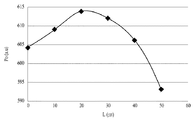
図6aは実施例による発光素子パッケージの光出力Poを示し、図6bは比較例と実施例の光出力Poを比較して示すグラフである。図6a及び図6bのそれぞれにおいて横軸は第2又は第4セグメントS2、S4の第1方向への長さ(L)を示し、縦軸は光出力Poを示す。 FIG. 6a is a graph showing the optical output Po of the light emitting device package according to the embodiment, and FIG. 6b is a graph showing the optical output Po of the comparative example and the embodiment in comparison. In each of FIGS. 6a and 6b, the horizontal axis represents the length (L) of the second or fourth segments S2 and S4 in the first direction, and the vertical axis represents the optical output Po.
前述した式1で示したように、第1幅W1と第2幅W2の比率が大きい場合、キャリアが均一に分配されなくて電流集中(current crowding)現象が発生することがある。これを改善するために、前述した実施例による発光素子パッケージ100は電流遮断層(CBL)の役目を行うように第1絶縁層142A、142Bを配置する。したがって、電流スプレディングが弱い部分にキャリアが円滑に注入されることができる。
As shown in the above equation 1, when the ratio of the first width W1 and the second width W2 is large, the carriers may not be uniformly distributed and a current concentrating phenomenon may occur. In order to improve this, the first insulating
図6aを参照すると、前述した実施例による発光素子パッケージ100において第1絶縁層142A、142Bが第2セグメントS2又は第4−2セグメントS4−2を含まない場合、つまり長さ(L)が‘0’の場合と比較すると、長さ(L)が0より大きくて40μm以下の場合に光出力Poが改善されることが分かる。
Referring to FIG. 6a, in the light emitting
また、比較例による発光素子パッケージは図2〜図4に示した発光素子パッケージにおいて第1絶縁層142A、142Bが省略された場合に相当する。図6bで、比較例による発光素子パッケージの光出力Poを“Ref”で表記した。例えば、図6bを参照すると、350mA又は500mAの動作電流で、第1絶縁層142A、142Bの第1方向への長さ(L)が20μm〜30μmの場合、比較例による発光素子パッケージより優れた光出力を有することが分かる。
Further, the light emitting element package according to the comparative example corresponds to the case where the first insulating
結局、前述したように、実施例による発光素子パッケージ100は、第1絶縁層142A、142Bによって、特に第2セグメントS2と第4−2セグメントS4−2によって発光素子パッケージの光学的特性が改善されることができる。特に、比較例による発光素子パッケージと比較すると、実施例による発光素子パッケージ100は高電流密度を有し、電流スプレディングを改善することができる。
After all, as described above, in the light emitting
図7はさらに他の実施例による発光素子パッケージ200の断面図を示す。
FIG. 7 shows a cross-sectional view of the light emitting
図7に示した発光素子パッケージ200は、図2に示した発光素子パッケージ100、第1及び第2リードフレーム212、214、絶縁部220、パッケージ胴体230、モールディング部材240及び第1及び第2半田部252、254を含むことができる。
The light emitting
第1及び第2リードフレーム212、214は第1及び第2ボンディングパッド132、134とそれぞれ電気的に連結されることができる。第1及び第2リードフレーム212、214は絶縁部220によって互いに電気的に離隔することができる。第1及び第2リードフレーム212、214のそれぞれは導電型物質、例えば金属でなることができ、実施例は第1及び第2リードフレーム212、214のそれぞれの物質の種類に限られない。
The first and second lead frames 212 and 214 can be electrically connected to the first and
絶縁部220は第1及び第2リードフレーム212、214の間に配置され、第1及び第2リードフレーム212、214を電気的に絶縁させる。このために、絶縁部220はSiO2、TiO2、ZrO2、Si3N4、Al2O3、又はMgF2の中で少なくとも1種を含むことができるが、実施例はこれに限られない。
The insulating
パッケージ胴体230は第1及び第2リードフレーム212、214と一緒にキャビティCを形成することができるが、実施例はこれに限られない。他の実施例によると、図7に例示したものとは違い、パッケージ胴体230のみでキャビティCを形成することもできる。若しくは、上面が平たいパッケージ胴体230上に隔壁(barrier wall)(図示せず)が配置され、隔壁とパッケージ胴体230の上面によってキャビティが規定されることもできる。
The
キャビティC内に図2に示した発光素子パッケージ100が配置できる。
The light emitting
パッケージ胴体230は、シリコン、合成樹脂又は金属を含んで形成できる。仮に、パッケージ胴体230が導電型物質、例えば金属物質でなる場合、第1及び第2リードフレーム212、214はパッケージ胴体230の一部であってもよい。この場合にも、第1及び第2リードフレーム212、214を形成するパッケージ胴体230は絶縁部220によって互いに電気的に分離されることができる。
The
モールディング部材240はキャビティC内に配置された発光素子パッケージ100を取り囲んで保護するように配置できる。モールディング部材240は、例えばシリコン(Si)で具現でき、蛍光体を含むので、発光素子パッケージ100から放出された光の波長を変化させることができる。蛍光体としては発光素子から発生した光を白色光に変換させることができるYAG系、TAG系、Silicate系、Sulfide系又はNitride系の中でいずれか1種の波長変換手段である蛍光物質を含むことができるが、実施例は蛍光体の種類に限られない。
The
YAG系及びTAG系蛍光物質としては、(Y、Tb、Lu、Sc、La、Gd、Sm)3(Al、Ga、In、Si、Fe)5(O、S)12:Ceの中で選択して使うことができ、Silicate系蛍光物質としては(Sr、Ba、Ca、Mg)2SiO4:(Eu、F、Cl)の中で選択して使うことができる。 As the YAG-based and TAG-based fluorescent substances, (Y, Tb, Lu, Sc, La, Gd, Sm) 3 (Al, Ga, In, Si, Fe) 5 (O, S) 12: Ce. As the silicate-based fluorescent substance, (Sr, Ba, Ca, Mg) 2SiO4 :( Eu, F, Cl) can be selected and used.
また、Sulfide系蛍光物質としては(Ca、Sr)S:Eu、(Sr、Ca、Ba)(Al、Ga)2S4:Euの中で選択して使うことができ、Nitride系蛍光体としては(Sr、Ca、Si、Al、O)N:Eu(例えば、CaAlSiN4:Euβ−SiAlON:Eu)又はCa−αSiAlON:Eu系の(Cax、My)(Si、Al)12(O、N)16(ここで、MはEu、Tb、Yb又はErの中で少なくとも1種の物質であり、0.05<(x+y)<0.3、0.02<x<0.27及び0.03<y<0.3)蛍光体成分の中で選択して使うことができる。 Further, the Sulfide-based fluorescent substance can be selected from (Ca, Sr) S: Eu and (Sr, Ca, Ba) (Al, Ga) 2S4: Eu, and can be used as the Nitride-based fluorescent substance ( Sr, Ca, Si, Al, O) N: Eu (eg, CaAlSiN4: Euβ-SiAlON: Eu) or Ca-αSiAlON: Eu system (Cax, My) (Si, Al) 12 (O, N) 16 ( Here, M is at least one substance among Eu, Tb, Yb or Er, and 0.05 <(x + y) <0.3, 0.02 <x <0.27 and 0.03 <y. <0.3) It can be selected and used from among the phosphor components.
赤色蛍光体としては、N(例えば、CaAlSiN3:Eu)を含む窒化物(Nitride)系蛍光体を使うことができる。このような窒化物系赤色蛍光体は硫化物(Sulfide)系蛍光体より熱、水分などの外部環境に対する信頼性に優れるだけでなく変色の危険が小さい。 As the red phosphor, a nitride-based phosphor containing N (for example, CaAlSiN3: Eu) can be used. Such a nitride-based red phosphor is not only more reliable in the external environment such as heat and moisture than a sulfide-based phosphor, but also has a smaller risk of discoloration.
第1半田部252は第1ボンディングパッド132と第1リードフレーム212の間に配置されてこれら132、212を電気的に連結する役目をする。第2半田部254は第2ボンディングパッド134と第2リードフレーム214の間に配置されてこれら134、214を電気的に連結する役目をする。第1及び第2半田部252、254のそれぞれは半田ペースト(solder paste)又は半田ボール(solder ball)であってもよいが、実施例はこれに限られない。
The
前述した第1及び第2半田部252、254は第1及び第2ボンディングパッド132、134を介して第1及び第2導電型半導体層122、126を第1及び第2リードフレーム212、214にそれぞれ電気的に連結させ、ワイヤを不要にすることができる。しかし、他の実施例によると、ワイヤで第1及び第2導電型半導体層122、126を第1及び第2リードフレーム212、214にそれぞれ連結させることもできる。
The first and
また、第1半田部252及び第2半田部254は省略することもできる。この場合、第1ボンディングパッド132が第1半田部252の役目をし、第2ボンディングパッド134が第2半田部254の役目をすることができる。すなわち、第1半田部252と第2半田部254が省略される場合、第1ボンディングパッド132は第1リードフレーム212と直接連結され、第2ボンディングパッド134は第2リードフレーム214と直接連結されることができる。
Further, the
実施例による発光素子パッケージは、複数が基板上に配列されることができ、発光素子パッケージの光経路上に光学部材である導光板、プリズムシート、拡散シートなどが配置できる。このような発光素子パッケージ、基板、光学部材はバックライトユニットとして機能することができる。 A plurality of light emitting element packages according to the embodiment can be arranged on a substrate, and a light guide plate, a prism sheet, a diffusion sheet, etc., which are optical members, can be arranged on the optical path of the light emitting element package. Such a light emitting element package, a substrate, and an optical member can function as a backlight unit.
また、実施例による発光素子パッケージは、表示装置、指示装置、照明装置に応用可能である。 Further, the light emitting element package according to the embodiment can be applied to a display device, an instruction device, and a lighting device.
ここで、表示装置は、ボトムカバーと、ボトムカバー上に配置される反射板と、光を放出する発光モジュールと、反射板の前方に配置され、発光モジュールから発散される光を前方に案内する導光板と、導光板の前方に配置されるプリズムシートを含む光学シートと、光学シートの前方に配置されるディスプレイパネルと、ディスプレイパネルと連結され、ディスプレイパネルに画像信号を供給する画像信号出力回路と、ディスプレイパネルの前方に配置されるカラーフィルターとを含むことができる。ここで、ボトムカバー、反射板、発光モジュール、導光板及び光学シートはバックライトユニット(Backlight Unit)を成すことができる。 Here, the display device is arranged in front of the bottom cover, the reflector arranged on the bottom cover, the light emitting module that emits light, and the light emitting module, and guides the light emitted from the light emitting module forward. An image signal output circuit that is connected to a light guide plate, an optical sheet including a prism sheet arranged in front of the light guide plate, a display panel arranged in front of the optical sheet, and a display panel to supply an image signal to the display panel. And a color filter located in front of the display panel. Here, the bottom cover, the reflector, the light emitting module, the light guide plate, and the optical sheet can form a backlight unit (Backlight Unit).
また、照明装置は、基板と実施例による発光素子パッケージを含む光源モジュール、光源モジュールの熱を発散させる放熱体、及び外部から受けた電気的信号を処理又は変換して光源モジュールに提供する電源提供部を含むことができる。例えば、照明装置は、ランプ、ヘッドランプ、又は街灯を含むことができる。 Further, the lighting device provides a light source module including a substrate and a light emitting element package according to an embodiment, a radiator that dissipates heat from the light source module, and a power source that processes or converts an electrical signal received from the outside and provides the light source module. Can include parts. For example, the luminaire can include lamps, headlamps, or street lights.
ヘッドランプは、基板上に配置される発光素子パッケージを含む発光モジュール、発光モジュールから照射される光を一定方向に、例えば前方に反射させるリフレクター(reflector)、リフレクターによって反射される光を前方に屈折させるレンズ、及びリフレクターによって反射されてレンズに向かう光の一部を遮断又は反射して設計者が望む配光パターンを成すようにするシェード(shade)を含むことができる。 The head lamp is a light emitting module including a light emitting element package arranged on a substrate, a reflector that reflects light emitted from the light emitting module in a certain direction, for example, forward, and refracts light reflected by the reflector forward. It can include a lens that causes the light to be reflected, and a shade that blocks or reflects a part of the light reflected by the reflector toward the lens to form a light distribution pattern desired by the designer.
以上で実施例に基づいて説明したが、これはただ例示にすぎないもので、本発明を限定するものではなく、本発明が属する分野の通常の知識を有する者であれば本実施例の本質的な特性を逸脱しない範疇内で以上で例示しなかった多様な変形及び応用が可能であることが分かるであろう。例えば、実施例に具体的に示した各構成要素は変形して実施することができるものである。そして、このような変形及び応用に係わる相違点は添付の請求範囲で規定する本発明の範囲に含まれるものとして解釈されなければならないであろう。
発明の実施のための形態
Although the above description has been made based on the examples, this is merely an example and does not limit the present invention, and the essence of the present examples is provided by a person who has ordinary knowledge in the field to which the present invention belongs. It will be seen that various modifications and applications not illustrated above are possible within the scope of not departing from the above characteristics. For example, each component specifically shown in the embodiment can be modified and implemented. And such differences relating to modifications and applications would have to be construed as being included in the scope of the invention as defined in the appended claims.
Embodiments for carrying out the invention
発明の実施のための形態は前述した“発明を実施するための形態”で充分に説明された。 The embodiment for carrying out the invention has been fully described in the above-mentioned "form for carrying out the invention".
本実施例による発光素子パッケージは、表示装置、指示装置、ランプやヘッドランプ又は街灯のような照明装置に応用可能である。 The light emitting element package according to this embodiment can be applied to a display device, an indicator device, and a lighting device such as a lamp, a headlamp, or a street light.
Claims (14)
前記基板の下側に配置され、第1導電型半導体層、活性層及び第2導電型半導体層を含む発光構造物と、
前記活性層及び前記第2導電型半導体層を貫いて前記第1導電型半導体層を露出させる貫通ホールに埋め込まれ、前記第1導電型半導体層と連結された第1ボンディングパッドと、
前記第1ボンディングパッドから離隔して前記第2導電型半導体層の下側に配置され、前記第2導電型半導体層と連結された第2ボンディングパッドと、
前記貫通ホールにおいて前記発光構造物の内側部に配置された第1セグメント及び前記第1セグメントから前記発光構造物の厚さ方向と交差する第1方向に延びて前記発光構造物の内側下部縁部に配置された第2セグメントを含む第1絶縁層と、
前記第1導電型半導体層と前記第1ボンディングパッドとの間に配置された第1電極と、
前記第2導電型半導体層の下側から前記第2セグメントの下側まで延びて配置され、前記第2導電型半導体層と連結された第2電極と、
前記貫通ホールにおいて前記第1絶縁層と前記第1ボンディングパッドとの間から前記第2セグメントの下側に配置された前記第2電極の下側まで延びて配置された第2絶縁層と、を含み、
前記第2電極が、
前記第2導電型半導体層の下側に配置された反射層と、
前記反射層と前記第2導電型半導体層の間に配置された透光電極層と、を含み、
前記透光電極層の幅は前記反射層の幅と同一である、発光素子パッケージ。 And the substrate,
A light emitting structure arranged under the substrate and including a first conductive semiconductor layer, an active layer, and a second conductive semiconductor layer .
A first bonding pad embedded in a through hole that penetrates the active layer and the second conductive semiconductor layer and exposes the first conductive semiconductor layer, and is connected to the first conductive semiconductor layer .
A second bonding pad, which is arranged under the second conductive semiconductor layer at a distance from the first bonding pad and is connected to the second conductive semiconductor layer ,
In the through hole, the first segment arranged inside the light emitting structure and the inner lower edge portion of the light emitting structure extending in the first direction intersecting the thickness direction of the light emitting structure from the first segment. a first insulating layer comprising a second segment disposed,
A first electrode arranged between the first conductive semiconductor layer and the first bonding pad ,
A second electrode extending from the lower side of the second conductive semiconductor layer to the lower side of the second segment and connected to the second conductive semiconductor layer .
And a second insulating layer disposed to extend to under the second electrode disposed on the lower side of the second segment from between the first bonding pad and the first insulating layer in the through-hole Including
The second electrode
A reflective layer arranged under the second conductive semiconductor layer and
A translucent electrode layer arranged between the reflective layer and the second conductive semiconductor layer is included.
A light emitting element package in which the width of the translucent electrode layer is the same as the width of the reflective layer .
Applications Claiming Priority (3)
| Application Number | Priority Date | Filing Date | Title |
|---|---|---|---|
| KR1020150042659A KR102434778B1 (en) | 2015-03-26 | 2015-03-26 | Light emitting device package |
| KR10-2015-0042659 | 2015-03-26 | ||
| PCT/KR2016/002612 WO2016153213A1 (en) | 2015-03-26 | 2016-03-16 | Light emitting diode package and lighting device |
Publications (3)
| Publication Number | Publication Date |
|---|---|
| JP2018509758A JP2018509758A (en) | 2018-04-05 |
| JP2018509758A5 JP2018509758A5 (en) | 2019-04-25 |
| JP6811715B2 true JP6811715B2 (en) | 2021-01-13 |
Family
ID=56977599
Family Applications (1)
| Application Number | Title | Priority Date | Filing Date |
|---|---|---|---|
| JP2017543339A Active JP6811715B2 (en) | 2015-03-26 | 2016-03-16 | Light emitting element package and lighting equipment |
Country Status (6)
| Country | Link |
|---|---|
| US (1) | US10381519B2 (en) |
| EP (1) | EP3276683B1 (en) |
| JP (1) | JP6811715B2 (en) |
| KR (1) | KR102434778B1 (en) |
| CN (1) | CN107431103A (en) |
| WO (1) | WO2016153213A1 (en) |
Families Citing this family (22)
| Publication number | Priority date | Publication date | Assignee | Title |
|---|---|---|---|---|
| KR20180073866A (en) * | 2016-12-23 | 2018-07-03 | 엘지이노텍 주식회사 | Semiconductor device |
| CN110214380B (en) * | 2017-01-25 | 2024-04-09 | 苏州立琻半导体有限公司 | Semiconductor device with a semiconductor layer having a plurality of semiconductor layers |
| KR102327777B1 (en) * | 2017-03-30 | 2021-11-17 | 쑤저우 레킨 세미컨덕터 컴퍼니 리미티드 | Semiconductor device, semiconductor device package, and object detecting apparatus |
| KR102308692B1 (en) * | 2017-03-30 | 2021-10-05 | 쑤저우 레킨 세미컨덕터 컴퍼니 리미티드 | Semiconductor device, method for fabricating semiconductor device, semiconductor device package, and object detecting apparatus |
| KR102311599B1 (en) * | 2017-03-30 | 2021-10-12 | 쑤저우 레킨 세미컨덕터 컴퍼니 리미티드 | Semiconductor device, method for fabricating semiconductor device, and semiconductor device package |
| US10998694B2 (en) | 2017-05-19 | 2021-05-04 | Lg Innotek Co., Ltd. | Laser diode |
| US10892297B2 (en) | 2017-11-27 | 2021-01-12 | Seoul Viosys Co., Ltd. | Light emitting diode (LED) stack for a display |
| US11527519B2 (en) | 2017-11-27 | 2022-12-13 | Seoul Viosys Co., Ltd. | LED unit for display and display apparatus having the same |
| US11282981B2 (en) | 2017-11-27 | 2022-03-22 | Seoul Viosys Co., Ltd. | Passivation covered light emitting unit stack |
| US10892296B2 (en) * | 2017-11-27 | 2021-01-12 | Seoul Viosys Co., Ltd. | Light emitting device having commonly connected LED sub-units |
| US10748881B2 (en) | 2017-12-05 | 2020-08-18 | Seoul Viosys Co., Ltd. | Light emitting device with LED stack for display and display apparatus having the same |
| US10886327B2 (en) | 2017-12-14 | 2021-01-05 | Seoul Viosys Co., Ltd. | Light emitting stacked structure and display device having the same |
| US11552057B2 (en) | 2017-12-20 | 2023-01-10 | Seoul Viosys Co., Ltd. | LED unit for display and display apparatus having the same |
| US11522006B2 (en) | 2017-12-21 | 2022-12-06 | Seoul Viosys Co., Ltd. | Light emitting stacked structure and display device having the same |
| US11552061B2 (en) | 2017-12-22 | 2023-01-10 | Seoul Viosys Co., Ltd. | Light emitting device with LED stack for display and display apparatus having the same |
| US11114499B2 (en) | 2018-01-02 | 2021-09-07 | Seoul Viosys Co., Ltd. | Display device having light emitting stacked structure |
| US10784240B2 (en) | 2018-01-03 | 2020-09-22 | Seoul Viosys Co., Ltd. | Light emitting device with LED stack for display and display apparatus having the same |
| CN111063778A (en) * | 2018-10-16 | 2020-04-24 | 合肥彩虹蓝光科技有限公司 | Light-emitting diode structure |
| KR102093816B1 (en) * | 2019-02-19 | 2020-03-26 | 엘지이노텍 주식회사 | Semiconductor device |
| CN109904285B (en) * | 2019-03-11 | 2022-04-05 | 合肥彩虹蓝光科技有限公司 | Light emitting diode chip and manufacturing method thereof |
| KR102212952B1 (en) * | 2019-05-07 | 2021-02-08 | 엘지이노텍 주식회사 | Semiconductor device |
| CN110931619A (en) * | 2019-11-20 | 2020-03-27 | 厦门士兰明镓化合物半导体有限公司 | Flip LED chip and manufacturing method thereof |
Family Cites Families (21)
| Publication number | Priority date | Publication date | Assignee | Title |
|---|---|---|---|---|
| JP2003124514A (en) * | 2001-10-17 | 2003-04-25 | Sony Corp | Semiconductor light emitting element and its manufacturing method |
| JP2006245156A (en) | 2005-03-02 | 2006-09-14 | Ledarts Opto Corp | Light emitting diode device equipped with flip chip structure |
| KR100609118B1 (en) | 2005-05-03 | 2006-08-08 | 삼성전기주식회사 | Flip chip light emitting diode and method of manufactureing the same |
| JP4359263B2 (en) | 2005-05-18 | 2009-11-04 | ローム株式会社 | Semiconductor light emitting device |
| KR100668964B1 (en) | 2005-09-27 | 2007-01-12 | 엘지전자 주식회사 | Light emitting device with nano-groove and method for fabricating the same |
| EP2023412A1 (en) | 2006-05-02 | 2009-02-11 | Mitsubishi Chemical Corporation | Semiconductor light-emitting device |
| US8368100B2 (en) * | 2007-11-14 | 2013-02-05 | Cree, Inc. | Semiconductor light emitting diodes having reflective structures and methods of fabricating same |
| JP5449786B2 (en) * | 2009-01-15 | 2014-03-19 | 昭和電工株式会社 | Silicon carbide semiconductor device and method for manufacturing silicon carbide semiconductor device |
| JP5334601B2 (en) * | 2009-01-21 | 2013-11-06 | 株式会社東芝 | Semiconductor light emitting diode element and semiconductor light emitting device |
| KR20110008550A (en) * | 2009-07-20 | 2011-01-27 | 삼성전자주식회사 | Light emitting element and fabricating method thereof |
| JP5152133B2 (en) | 2009-09-18 | 2013-02-27 | 豊田合成株式会社 | Light emitting element |
| KR101704022B1 (en) * | 2010-02-12 | 2017-02-07 | 엘지이노텍 주식회사 | Light emitting device, method for fabricating the same and light emitting device package |
| KR101630152B1 (en) * | 2010-02-24 | 2016-06-14 | 엘지디스플레이 주식회사 | Hybrid light emitting diode chip and light emitting diode device having the same, and manufacturing method thereof |
| KR101142965B1 (en) | 2010-09-24 | 2012-05-08 | 서울반도체 주식회사 | Wafer-level light emitting diode package and method of fabricating the same |
| US9070851B2 (en) | 2010-09-24 | 2015-06-30 | Seoul Semiconductor Co., Ltd. | Wafer-level light emitting diode package and method of fabricating the same |
| JP5754173B2 (en) | 2011-03-01 | 2015-07-29 | ソニー株式会社 | Light emitting unit and display device |
| KR20130097363A (en) * | 2012-02-24 | 2013-09-03 | 삼성전자주식회사 | Light emitting device and manufacturing method thereof |
| KR101362081B1 (en) | 2012-12-28 | 2014-02-13 | 주식회사 위뷰 | Light emitting device |
| JP2014150245A (en) * | 2013-01-08 | 2014-08-21 | Rohm Co Ltd | Light-emitting element and light-emitting element package |
| KR101958419B1 (en) * | 2013-01-29 | 2019-03-14 | 삼성전자 주식회사 | Semiconductor light emitting device |
| KR102086365B1 (en) * | 2013-04-19 | 2020-03-09 | 삼성전자주식회사 | Semiconductor light emitting device |
-
2015
- 2015-03-26 KR KR1020150042659A patent/KR102434778B1/en active IP Right Grant
-
2016
- 2016-03-16 JP JP2017543339A patent/JP6811715B2/en active Active
- 2016-03-16 EP EP16769031.2A patent/EP3276683B1/en active Active
- 2016-03-16 US US15/550,955 patent/US10381519B2/en active Active
- 2016-03-16 WO PCT/KR2016/002612 patent/WO2016153213A1/en active Application Filing
- 2016-03-16 CN CN201680016088.3A patent/CN107431103A/en active Pending
Also Published As
| Publication number | Publication date |
|---|---|
| KR20160115301A (en) | 2016-10-06 |
| WO2016153213A1 (en) | 2016-09-29 |
| EP3276683B1 (en) | 2020-03-11 |
| EP3276683A4 (en) | 2018-09-12 |
| EP3276683A1 (en) | 2018-01-31 |
| JP2018509758A (en) | 2018-04-05 |
| US20180026163A1 (en) | 2018-01-25 |
| CN107431103A (en) | 2017-12-01 |
| US10381519B2 (en) | 2019-08-13 |
| KR102434778B1 (en) | 2022-08-23 |
Similar Documents
| Publication | Publication Date | Title |
|---|---|---|
| JP6811715B2 (en) | Light emitting element package and lighting equipment | |
| JP6712474B2 (en) | Light emitting device and light emitting device package including the same | |
| JP6783048B2 (en) | Light emitting element package and lighting equipment including it | |
| KR102038443B1 (en) | Light emitting device and light emitting device package | |
| JP6796078B2 (en) | Light emitting element and light emitting element package | |
| KR102569249B1 (en) | Light emitting device package | |
| JP6802625B2 (en) | A light emitting element, a light emitting element package, and a lighting device including the package. | |
| KR102464028B1 (en) | Light emitting device package, and light emitting apparatus including the package | |
| KR102408617B1 (en) | Light emitting device package, and light emitting apparatus including the package | |
| KR20160115868A (en) | Light emitting device, light emitting device package including the device, and lighting apparatus including the package | |
| KR102455091B1 (en) | Light emitting device and light emitting device package including the device | |
| KR102445547B1 (en) | Light emitting device and light emitting device package including the device | |
| KR102320866B1 (en) | Light emitting device and light emitting device package | |
| KR101941034B1 (en) | Light emitting device package and lighting apparatus | |
| KR102343497B1 (en) | Light emitting device and light emitting device package including the device | |
| KR102326926B1 (en) | Light emitting device, and lighting emitting device package | |
| KR20160036293A (en) | Light emitting device package |
Legal Events
| Date | Code | Title | Description |
|---|---|---|---|
| A521 | Request for written amendment filed |
Free format text: JAPANESE INTERMEDIATE CODE: A523 Effective date: 20170927 |
|
| A521 | Request for written amendment filed |
Free format text: JAPANESE INTERMEDIATE CODE: A523 Effective date: 20190313 |
|
| A621 | Written request for application examination |
Free format text: JAPANESE INTERMEDIATE CODE: A621 Effective date: 20190313 |
|
| A977 | Report on retrieval |
Free format text: JAPANESE INTERMEDIATE CODE: A971007 Effective date: 20200228 |
|
| A131 | Notification of reasons for refusal |
Free format text: JAPANESE INTERMEDIATE CODE: A131 Effective date: 20200407 |
|
| A521 | Request for written amendment filed |
Free format text: JAPANESE INTERMEDIATE CODE: A523 Effective date: 20200706 |
|
| TRDD | Decision of grant or rejection written | ||
| A01 | Written decision to grant a patent or to grant a registration (utility model) |
Free format text: JAPANESE INTERMEDIATE CODE: A01 Effective date: 20201208 |
|
| A61 | First payment of annual fees (during grant procedure) |
Free format text: JAPANESE INTERMEDIATE CODE: A61 Effective date: 20201215 |
|
| R150 | Certificate of patent or registration of utility model |
Ref document number: 6811715 Country of ref document: JP Free format text: JAPANESE INTERMEDIATE CODE: R150 |
|
| S111 | Request for change of ownership or part of ownership |
Free format text: JAPANESE INTERMEDIATE CODE: R313113 |
|
| R350 | Written notification of registration of transfer |
Free format text: JAPANESE INTERMEDIATE CODE: R350 |
|
| R250 | Receipt of annual fees |
Free format text: JAPANESE INTERMEDIATE CODE: R250 |