JP6777148B2 - Semiconductor device - Google Patents
Semiconductor device Download PDFInfo
- Publication number
- JP6777148B2 JP6777148B2 JP2018530284A JP2018530284A JP6777148B2 JP 6777148 B2 JP6777148 B2 JP 6777148B2 JP 2018530284 A JP2018530284 A JP 2018530284A JP 2018530284 A JP2018530284 A JP 2018530284A JP 6777148 B2 JP6777148 B2 JP 6777148B2
- Authority
- JP
- Japan
- Prior art keywords
- solder
- intermediate plate
- semiconductor device
- semiconductor chip
- electrode substrate
- Prior art date
- Legal status (The legal status is an assumption and is not a legal conclusion. Google has not performed a legal analysis and makes no representation as to the accuracy of the status listed.)
- Active
Links
- 239000004065 semiconductor Substances 0.000 title claims description 132
- 229910000679 solder Inorganic materials 0.000 claims description 94
- 239000000758 substrate Substances 0.000 claims description 49
- 239000000463 material Substances 0.000 claims description 23
- 238000007747 plating Methods 0.000 claims description 9
- 229910052782 aluminium Inorganic materials 0.000 claims description 8
- XAGFODPZIPBFFR-UHFFFAOYSA-N aluminium Chemical group [Al] XAGFODPZIPBFFR-UHFFFAOYSA-N 0.000 claims description 8
- 239000010949 copper Substances 0.000 claims description 8
- ZOKXTWBITQBERF-UHFFFAOYSA-N Molybdenum Chemical group [Mo] ZOKXTWBITQBERF-UHFFFAOYSA-N 0.000 claims description 5
- PXHVJJICTQNCMI-UHFFFAOYSA-N Nickel Chemical group [Ni] PXHVJJICTQNCMI-UHFFFAOYSA-N 0.000 claims description 5
- 229910052750 molybdenum Inorganic materials 0.000 claims description 5
- 239000011733 molybdenum Substances 0.000 claims description 5
- RYGMFSIKBFXOCR-UHFFFAOYSA-N Copper Chemical group [Cu] RYGMFSIKBFXOCR-UHFFFAOYSA-N 0.000 claims description 4
- 150000001875 compounds Chemical class 0.000 claims description 4
- 229910052802 copper Inorganic materials 0.000 claims description 4
- OKTJSMMVPCPJKN-UHFFFAOYSA-N Carbon Chemical group [C] OKTJSMMVPCPJKN-UHFFFAOYSA-N 0.000 claims description 2
- 229910052799 carbon Inorganic materials 0.000 claims description 2
- 229910052759 nickel Inorganic materials 0.000 claims description 2
- 239000003566 sealing material Substances 0.000 description 6
- 239000004020 conductor Substances 0.000 description 5
- 238000001816 cooling Methods 0.000 description 4
- 238000004519 manufacturing process Methods 0.000 description 4
- 238000004080 punching Methods 0.000 description 4
- 239000011347 resin Substances 0.000 description 4
- 229920005989 resin Polymers 0.000 description 4
- HBMJWWWQQXIZIP-UHFFFAOYSA-N silicon carbide Chemical compound [Si+]#[C-] HBMJWWWQQXIZIP-UHFFFAOYSA-N 0.000 description 4
- 229910010271 silicon carbide Inorganic materials 0.000 description 4
- 238000005266 casting Methods 0.000 description 3
- 229910052710 silicon Inorganic materials 0.000 description 3
- 239000010703 silicon Substances 0.000 description 3
- 239000000498 cooling water Substances 0.000 description 2
- 230000000694 effects Effects 0.000 description 2
- 229910000765 intermetallic Inorganic materials 0.000 description 2
- 238000005304 joining Methods 0.000 description 2
- 229910052751 metal Inorganic materials 0.000 description 2
- 239000002184 metal Substances 0.000 description 2
- 238000000034 method Methods 0.000 description 2
- 238000005096 rolling process Methods 0.000 description 2
- 239000011800 void material Substances 0.000 description 2
- 229910017944 Ag—Cu Inorganic materials 0.000 description 1
- 229910002601 GaN Inorganic materials 0.000 description 1
- JMASRVWKEDWRBT-UHFFFAOYSA-N Gallium nitride Chemical compound [Ga]#N JMASRVWKEDWRBT-UHFFFAOYSA-N 0.000 description 1
- HBBGRARXTFLTSG-UHFFFAOYSA-N Lithium ion Chemical compound [Li+] HBBGRARXTFLTSG-UHFFFAOYSA-N 0.000 description 1
- 229910020836 Sn-Ag Inorganic materials 0.000 description 1
- 229910020888 Sn-Cu Inorganic materials 0.000 description 1
- 229910020988 Sn—Ag Inorganic materials 0.000 description 1
- 229910019204 Sn—Cu Inorganic materials 0.000 description 1
- 230000002411 adverse Effects 0.000 description 1
- 230000007797 corrosion Effects 0.000 description 1
- 238000005260 corrosion Methods 0.000 description 1
- 230000007547 defect Effects 0.000 description 1
- 230000006866 deterioration Effects 0.000 description 1
- 238000010586 diagram Methods 0.000 description 1
- 239000010432 diamond Substances 0.000 description 1
- 229910003460 diamond Inorganic materials 0.000 description 1
- 238000009713 electroplating Methods 0.000 description 1
- 238000010438 heat treatment Methods 0.000 description 1
- 229910001416 lithium ion Inorganic materials 0.000 description 1
- 238000002844 melting Methods 0.000 description 1
- 230000008018 melting Effects 0.000 description 1
- 239000007769 metal material Substances 0.000 description 1
- 230000002093 peripheral effect Effects 0.000 description 1
- 238000004382 potting Methods 0.000 description 1
- 230000005855 radiation Effects 0.000 description 1
- 239000007790 solid phase Substances 0.000 description 1
- 238000004544 sputter deposition Methods 0.000 description 1
- 238000007740 vapor deposition Methods 0.000 description 1
- 238000001947 vapour-phase growth Methods 0.000 description 1
Images


Classifications
-
- H—ELECTRICITY
- H01—ELECTRIC ELEMENTS
- H01L—SEMICONDUCTOR DEVICES NOT COVERED BY CLASS H10
- H01L24/00—Arrangements for connecting or disconnecting semiconductor or solid-state bodies; Methods or apparatus related thereto
- H01L24/80—Methods for connecting semiconductor or other solid state bodies using means for bonding being attached to, or being formed on, the surface to be connected
- H01L24/84—Methods for connecting semiconductor or other solid state bodies using means for bonding being attached to, or being formed on, the surface to be connected using a strap connector
-
- H—ELECTRICITY
- H01—ELECTRIC ELEMENTS
- H01L—SEMICONDUCTOR DEVICES NOT COVERED BY CLASS H10
- H01L21/00—Processes or apparatus adapted for the manufacture or treatment of semiconductor or solid state devices or of parts thereof
- H01L21/02—Manufacture or treatment of semiconductor devices or of parts thereof
- H01L21/04—Manufacture or treatment of semiconductor devices or of parts thereof the devices having potential barriers, e.g. a PN junction, depletion layer or carrier concentration layer
- H01L21/50—Assembly of semiconductor devices using processes or apparatus not provided for in a single one of the subgroups H01L21/06 - H01L21/326, e.g. sealing of a cap to a base of a container
- H01L21/52—Mounting semiconductor bodies in containers
-
- H—ELECTRICITY
- H01—ELECTRIC ELEMENTS
- H01L—SEMICONDUCTOR DEVICES NOT COVERED BY CLASS H10
- H01L23/00—Details of semiconductor or other solid state devices
- H01L23/48—Arrangements for conducting electric current to or from the solid state body in operation, e.g. leads, terminal arrangements ; Selection of materials therefor
-
- H—ELECTRICITY
- H01—ELECTRIC ELEMENTS
- H01L—SEMICONDUCTOR DEVICES NOT COVERED BY CLASS H10
- H01L24/00—Arrangements for connecting or disconnecting semiconductor or solid-state bodies; Methods or apparatus related thereto
- H01L24/01—Means for bonding being attached to, or being formed on, the surface to be connected, e.g. chip-to-package, die-attach, "first-level" interconnects; Manufacturing methods related thereto
- H01L24/26—Layer connectors, e.g. plate connectors, solder or adhesive layers; Manufacturing methods related thereto
- H01L24/28—Structure, shape, material or disposition of the layer connectors prior to the connecting process
- H01L24/29—Structure, shape, material or disposition of the layer connectors prior to the connecting process of an individual layer connector
-
- H—ELECTRICITY
- H01—ELECTRIC ELEMENTS
- H01L—SEMICONDUCTOR DEVICES NOT COVERED BY CLASS H10
- H01L24/00—Arrangements for connecting or disconnecting semiconductor or solid-state bodies; Methods or apparatus related thereto
- H01L24/01—Means for bonding being attached to, or being formed on, the surface to be connected, e.g. chip-to-package, die-attach, "first-level" interconnects; Manufacturing methods related thereto
- H01L24/26—Layer connectors, e.g. plate connectors, solder or adhesive layers; Manufacturing methods related thereto
- H01L24/28—Structure, shape, material or disposition of the layer connectors prior to the connecting process
- H01L24/30—Structure, shape, material or disposition of the layer connectors prior to the connecting process of a plurality of layer connectors
-
- H—ELECTRICITY
- H01—ELECTRIC ELEMENTS
- H01L—SEMICONDUCTOR DEVICES NOT COVERED BY CLASS H10
- H01L24/00—Arrangements for connecting or disconnecting semiconductor or solid-state bodies; Methods or apparatus related thereto
- H01L24/01—Means for bonding being attached to, or being formed on, the surface to be connected, e.g. chip-to-package, die-attach, "first-level" interconnects; Manufacturing methods related thereto
- H01L24/26—Layer connectors, e.g. plate connectors, solder or adhesive layers; Manufacturing methods related thereto
- H01L24/31—Structure, shape, material or disposition of the layer connectors after the connecting process
- H01L24/32—Structure, shape, material or disposition of the layer connectors after the connecting process of an individual layer connector
-
- H—ELECTRICITY
- H01—ELECTRIC ELEMENTS
- H01L—SEMICONDUCTOR DEVICES NOT COVERED BY CLASS H10
- H01L24/00—Arrangements for connecting or disconnecting semiconductor or solid-state bodies; Methods or apparatus related thereto
- H01L24/01—Means for bonding being attached to, or being formed on, the surface to be connected, e.g. chip-to-package, die-attach, "first-level" interconnects; Manufacturing methods related thereto
- H01L24/26—Layer connectors, e.g. plate connectors, solder or adhesive layers; Manufacturing methods related thereto
- H01L24/31—Structure, shape, material or disposition of the layer connectors after the connecting process
- H01L24/33—Structure, shape, material or disposition of the layer connectors after the connecting process of a plurality of layer connectors
-
- H—ELECTRICITY
- H01—ELECTRIC ELEMENTS
- H01L—SEMICONDUCTOR DEVICES NOT COVERED BY CLASS H10
- H01L24/00—Arrangements for connecting or disconnecting semiconductor or solid-state bodies; Methods or apparatus related thereto
- H01L24/80—Methods for connecting semiconductor or other solid state bodies using means for bonding being attached to, or being formed on, the surface to be connected
- H01L24/83—Methods for connecting semiconductor or other solid state bodies using means for bonding being attached to, or being formed on, the surface to be connected using a layer connector
-
- H—ELECTRICITY
- H01—ELECTRIC ELEMENTS
- H01L—SEMICONDUCTOR DEVICES NOT COVERED BY CLASS H10
- H01L2224/00—Indexing scheme for arrangements for connecting or disconnecting semiconductor or solid-state bodies and methods related thereto as covered by H01L24/00
- H01L2224/01—Means for bonding being attached to, or being formed on, the surface to be connected, e.g. chip-to-package, die-attach, "first-level" interconnects; Manufacturing methods related thereto
- H01L2224/26—Layer connectors, e.g. plate connectors, solder or adhesive layers; Manufacturing methods related thereto
- H01L2224/2612—Auxiliary members for layer connectors, e.g. spacers
- H01L2224/26152—Auxiliary members for layer connectors, e.g. spacers being formed on an item to be connected not being a semiconductor or solid-state body
- H01L2224/26155—Reinforcing structures
-
- H—ELECTRICITY
- H01—ELECTRIC ELEMENTS
- H01L—SEMICONDUCTOR DEVICES NOT COVERED BY CLASS H10
- H01L2224/00—Indexing scheme for arrangements for connecting or disconnecting semiconductor or solid-state bodies and methods related thereto as covered by H01L24/00
- H01L2224/01—Means for bonding being attached to, or being formed on, the surface to be connected, e.g. chip-to-package, die-attach, "first-level" interconnects; Manufacturing methods related thereto
- H01L2224/26—Layer connectors, e.g. plate connectors, solder or adhesive layers; Manufacturing methods related thereto
- H01L2224/28—Structure, shape, material or disposition of the layer connectors prior to the connecting process
- H01L2224/29—Structure, shape, material or disposition of the layer connectors prior to the connecting process of an individual layer connector
- H01L2224/29001—Core members of the layer connector
- H01L2224/29099—Material
- H01L2224/291—Material with a principal constituent of the material being a metal or a metalloid, e.g. boron [B], silicon [Si], germanium [Ge], arsenic [As], antimony [Sb], tellurium [Te] and polonium [Po], and alloys thereof
- H01L2224/29138—Material with a principal constituent of the material being a metal or a metalloid, e.g. boron [B], silicon [Si], germanium [Ge], arsenic [As], antimony [Sb], tellurium [Te] and polonium [Po], and alloys thereof the principal constituent melting at a temperature of greater than or equal to 950°C and less than 1550°C
- H01L2224/29155—Nickel [Ni] as principal constituent
-
- H—ELECTRICITY
- H01—ELECTRIC ELEMENTS
- H01L—SEMICONDUCTOR DEVICES NOT COVERED BY CLASS H10
- H01L2224/00—Indexing scheme for arrangements for connecting or disconnecting semiconductor or solid-state bodies and methods related thereto as covered by H01L24/00
- H01L2224/01—Means for bonding being attached to, or being formed on, the surface to be connected, e.g. chip-to-package, die-attach, "first-level" interconnects; Manufacturing methods related thereto
- H01L2224/26—Layer connectors, e.g. plate connectors, solder or adhesive layers; Manufacturing methods related thereto
- H01L2224/28—Structure, shape, material or disposition of the layer connectors prior to the connecting process
- H01L2224/30—Structure, shape, material or disposition of the layer connectors prior to the connecting process of a plurality of layer connectors
- H01L2224/301—Disposition
- H01L2224/3018—Disposition being disposed on at least two different sides of the body, e.g. dual array
- H01L2224/30181—On opposite sides of the body
-
- H—ELECTRICITY
- H01—ELECTRIC ELEMENTS
- H01L—SEMICONDUCTOR DEVICES NOT COVERED BY CLASS H10
- H01L2224/00—Indexing scheme for arrangements for connecting or disconnecting semiconductor or solid-state bodies and methods related thereto as covered by H01L24/00
- H01L2224/01—Means for bonding being attached to, or being formed on, the surface to be connected, e.g. chip-to-package, die-attach, "first-level" interconnects; Manufacturing methods related thereto
- H01L2224/26—Layer connectors, e.g. plate connectors, solder or adhesive layers; Manufacturing methods related thereto
- H01L2224/31—Structure, shape, material or disposition of the layer connectors after the connecting process
- H01L2224/32—Structure, shape, material or disposition of the layer connectors after the connecting process of an individual layer connector
- H01L2224/321—Disposition
- H01L2224/32151—Disposition the layer connector connecting between a semiconductor or solid-state body and an item not being a semiconductor or solid-state body, e.g. chip-to-substrate, chip-to-passive
- H01L2224/32221—Disposition the layer connector connecting between a semiconductor or solid-state body and an item not being a semiconductor or solid-state body, e.g. chip-to-substrate, chip-to-passive the body and the item being stacked
- H01L2224/32245—Disposition the layer connector connecting between a semiconductor or solid-state body and an item not being a semiconductor or solid-state body, e.g. chip-to-substrate, chip-to-passive the body and the item being stacked the item being metallic
-
- H—ELECTRICITY
- H01—ELECTRIC ELEMENTS
- H01L—SEMICONDUCTOR DEVICES NOT COVERED BY CLASS H10
- H01L2224/00—Indexing scheme for arrangements for connecting or disconnecting semiconductor or solid-state bodies and methods related thereto as covered by H01L24/00
- H01L2224/01—Means for bonding being attached to, or being formed on, the surface to be connected, e.g. chip-to-package, die-attach, "first-level" interconnects; Manufacturing methods related thereto
- H01L2224/26—Layer connectors, e.g. plate connectors, solder or adhesive layers; Manufacturing methods related thereto
- H01L2224/31—Structure, shape, material or disposition of the layer connectors after the connecting process
- H01L2224/33—Structure, shape, material or disposition of the layer connectors after the connecting process of a plurality of layer connectors
- H01L2224/331—Disposition
- H01L2224/3318—Disposition being disposed on at least two different sides of the body, e.g. dual array
- H01L2224/33181—On opposite sides of the body
-
- H—ELECTRICITY
- H01—ELECTRIC ELEMENTS
- H01L—SEMICONDUCTOR DEVICES NOT COVERED BY CLASS H10
- H01L2224/00—Indexing scheme for arrangements for connecting or disconnecting semiconductor or solid-state bodies and methods related thereto as covered by H01L24/00
- H01L2224/01—Means for bonding being attached to, or being formed on, the surface to be connected, e.g. chip-to-package, die-attach, "first-level" interconnects; Manufacturing methods related thereto
- H01L2224/34—Strap connectors, e.g. copper straps for grounding power devices; Manufacturing methods related thereto
- H01L2224/36—Structure, shape, material or disposition of the strap connectors prior to the connecting process
- H01L2224/37—Structure, shape, material or disposition of the strap connectors prior to the connecting process of an individual strap connector
- H01L2224/37001—Core members of the connector
- H01L2224/37099—Material
- H01L2224/371—Material with a principal constituent of the material being a metal or a metalloid, e.g. boron [B], silicon [Si], germanium [Ge], arsenic [As], antimony [Sb], tellurium [Te] and polonium [Po], and alloys thereof
- H01L2224/37138—Material with a principal constituent of the material being a metal or a metalloid, e.g. boron [B], silicon [Si], germanium [Ge], arsenic [As], antimony [Sb], tellurium [Te] and polonium [Po], and alloys thereof the principal constituent melting at a temperature of greater than or equal to 950°C and less than 1550°C
- H01L2224/37147—Copper [Cu] as principal constituent
-
- H—ELECTRICITY
- H01—ELECTRIC ELEMENTS
- H01L—SEMICONDUCTOR DEVICES NOT COVERED BY CLASS H10
- H01L2224/00—Indexing scheme for arrangements for connecting or disconnecting semiconductor or solid-state bodies and methods related thereto as covered by H01L24/00
- H01L2224/01—Means for bonding being attached to, or being formed on, the surface to be connected, e.g. chip-to-package, die-attach, "first-level" interconnects; Manufacturing methods related thereto
- H01L2224/34—Strap connectors, e.g. copper straps for grounding power devices; Manufacturing methods related thereto
- H01L2224/39—Structure, shape, material or disposition of the strap connectors after the connecting process
- H01L2224/40—Structure, shape, material or disposition of the strap connectors after the connecting process of an individual strap connector
- H01L2224/401—Disposition
- H01L2224/40151—Connecting between a semiconductor or solid-state body and an item not being a semiconductor or solid-state body, e.g. chip-to-substrate, chip-to-passive
- H01L2224/40221—Connecting between a semiconductor or solid-state body and an item not being a semiconductor or solid-state body, e.g. chip-to-substrate, chip-to-passive the body and the item being stacked
- H01L2224/40245—Connecting between a semiconductor or solid-state body and an item not being a semiconductor or solid-state body, e.g. chip-to-substrate, chip-to-passive the body and the item being stacked the item being metallic
-
- H—ELECTRICITY
- H01—ELECTRIC ELEMENTS
- H01L—SEMICONDUCTOR DEVICES NOT COVERED BY CLASS H10
- H01L2224/00—Indexing scheme for arrangements for connecting or disconnecting semiconductor or solid-state bodies and methods related thereto as covered by H01L24/00
- H01L2224/73—Means for bonding being of different types provided for in two or more of groups H01L2224/10, H01L2224/18, H01L2224/26, H01L2224/34, H01L2224/42, H01L2224/50, H01L2224/63, H01L2224/71
- H01L2224/732—Location after the connecting process
- H01L2224/73251—Location after the connecting process on different surfaces
- H01L2224/73265—Layer and wire connectors
-
- H—ELECTRICITY
- H01—ELECTRIC ELEMENTS
- H01L—SEMICONDUCTOR DEVICES NOT COVERED BY CLASS H10
- H01L2224/00—Indexing scheme for arrangements for connecting or disconnecting semiconductor or solid-state bodies and methods related thereto as covered by H01L24/00
- H01L2224/80—Methods for connecting semiconductor or other solid state bodies using means for bonding being attached to, or being formed on, the surface to be connected
- H01L2224/83—Methods for connecting semiconductor or other solid state bodies using means for bonding being attached to, or being formed on, the surface to be connected using a layer connector
- H01L2224/83007—Methods for connecting semiconductor or other solid state bodies using means for bonding being attached to, or being formed on, the surface to be connected using a layer connector involving a permanent auxiliary member being left in the finished device, e.g. aids for holding or protecting the layer connector during or after the bonding process
-
- H—ELECTRICITY
- H01—ELECTRIC ELEMENTS
- H01L—SEMICONDUCTOR DEVICES NOT COVERED BY CLASS H10
- H01L2224/00—Indexing scheme for arrangements for connecting or disconnecting semiconductor or solid-state bodies and methods related thereto as covered by H01L24/00
- H01L2224/80—Methods for connecting semiconductor or other solid state bodies using means for bonding being attached to, or being formed on, the surface to be connected
- H01L2224/83—Methods for connecting semiconductor or other solid state bodies using means for bonding being attached to, or being formed on, the surface to be connected using a layer connector
- H01L2224/83053—Bonding environment
- H01L2224/83054—Composition of the atmosphere
- H01L2224/83065—Composition of the atmosphere being reducing
-
- H—ELECTRICITY
- H01—ELECTRIC ELEMENTS
- H01L—SEMICONDUCTOR DEVICES NOT COVERED BY CLASS H10
- H01L2224/00—Indexing scheme for arrangements for connecting or disconnecting semiconductor or solid-state bodies and methods related thereto as covered by H01L24/00
- H01L2224/80—Methods for connecting semiconductor or other solid state bodies using means for bonding being attached to, or being formed on, the surface to be connected
- H01L2224/83—Methods for connecting semiconductor or other solid state bodies using means for bonding being attached to, or being formed on, the surface to be connected using a layer connector
- H01L2224/838—Bonding techniques
- H01L2224/83801—Soldering or alloying
- H01L2224/83815—Reflow soldering
-
- H—ELECTRICITY
- H01—ELECTRIC ELEMENTS
- H01L—SEMICONDUCTOR DEVICES NOT COVERED BY CLASS H10
- H01L2224/00—Indexing scheme for arrangements for connecting or disconnecting semiconductor or solid-state bodies and methods related thereto as covered by H01L24/00
- H01L2224/80—Methods for connecting semiconductor or other solid state bodies using means for bonding being attached to, or being formed on, the surface to be connected
- H01L2224/84—Methods for connecting semiconductor or other solid state bodies using means for bonding being attached to, or being formed on, the surface to be connected using a strap connector
- H01L2224/848—Bonding techniques
- H01L2224/84801—Soldering or alloying
-
- H—ELECTRICITY
- H01—ELECTRIC ELEMENTS
- H01L—SEMICONDUCTOR DEVICES NOT COVERED BY CLASS H10
- H01L2924/00—Indexing scheme for arrangements or methods for connecting or disconnecting semiconductor or solid-state bodies as covered by H01L24/00
- H01L2924/0001—Technical content checked by a classifier
- H01L2924/00012—Relevant to the scope of the group, the symbol of which is combined with the symbol of this group
-
- H—ELECTRICITY
- H01—ELECTRIC ELEMENTS
- H01L—SEMICONDUCTOR DEVICES NOT COVERED BY CLASS H10
- H01L2924/00—Indexing scheme for arrangements or methods for connecting or disconnecting semiconductor or solid-state bodies as covered by H01L24/00
- H01L2924/0001—Technical content checked by a classifier
- H01L2924/00014—Technical content checked by a classifier the subject-matter covered by the group, the symbol of which is combined with the symbol of this group, being disclosed without further technical details
-
- H—ELECTRICITY
- H01—ELECTRIC ELEMENTS
- H01L—SEMICONDUCTOR DEVICES NOT COVERED BY CLASS H10
- H01L2924/00—Indexing scheme for arrangements or methods for connecting or disconnecting semiconductor or solid-state bodies as covered by H01L24/00
- H01L2924/013—Alloys
- H01L2924/014—Solder alloys
-
- H—ELECTRICITY
- H01—ELECTRIC ELEMENTS
- H01L—SEMICONDUCTOR DEVICES NOT COVERED BY CLASS H10
- H01L2924/00—Indexing scheme for arrangements or methods for connecting or disconnecting semiconductor or solid-state bodies as covered by H01L24/00
- H01L2924/10—Details of semiconductor or other solid state devices to be connected
- H01L2924/102—Material of the semiconductor or solid state bodies
- H01L2924/1025—Semiconducting materials
- H01L2924/1026—Compound semiconductors
- H01L2924/1027—IV
- H01L2924/10272—Silicon Carbide [SiC]
-
- H—ELECTRICITY
- H01—ELECTRIC ELEMENTS
- H01L—SEMICONDUCTOR DEVICES NOT COVERED BY CLASS H10
- H01L2924/00—Indexing scheme for arrangements or methods for connecting or disconnecting semiconductor or solid-state bodies as covered by H01L24/00
- H01L2924/15—Details of package parts other than the semiconductor or other solid state devices to be connected
- H01L2924/181—Encapsulation
-
- H—ELECTRICITY
- H01—ELECTRIC ELEMENTS
- H01L—SEMICONDUCTOR DEVICES NOT COVERED BY CLASS H10
- H01L2924/00—Indexing scheme for arrangements or methods for connecting or disconnecting semiconductor or solid-state bodies as covered by H01L24/00
- H01L2924/30—Technical effects
- H01L2924/35—Mechanical effects
- H01L2924/351—Thermal stress
Landscapes
- Engineering & Computer Science (AREA)
- Computer Hardware Design (AREA)
- Microelectronics & Electronic Packaging (AREA)
- Power Engineering (AREA)
- Physics & Mathematics (AREA)
- Condensed Matter Physics & Semiconductors (AREA)
- General Physics & Mathematics (AREA)
- Manufacturing & Machinery (AREA)
- Cooling Or The Like Of Semiconductors Or Solid State Devices (AREA)
- Die Bonding (AREA)
Description
本発明は、IGBT、MOSFET、Diodeなどの電力用半導体装置に関する。 The present invention relates to power semiconductor devices such as IGBTs, MOSFETs, and Diodes.
アルミ電極基板にはんだを介して半導体チップを接合し、半導体チップの上面にはんだを介して銅電極を接合した半導体装置が開示されている(例えば、特許文献1参照)。 A semiconductor device in which a semiconductor chip is bonded to an aluminum electrode substrate via solder and a copper electrode is bonded to the upper surface of the semiconductor chip via solder is disclosed (see, for example, Patent Document 1).
しかし、冷熱サイクル及びパワーサイクルの温度範囲、即ち半導体装置の使用温度範囲でアルミ電極基板とはんだとの耐力関係が逆転する点が存在する。このため、アルミ電極基板とはんだがそれぞれ変形し、元の位置に戻らなくなる。さらに変形量が蓄積して大きくなると、最終的に半導体チップが変形して信頼性が低下するという問題があった。特に、高温対応のSiCチップなどでは、使用温度範囲が広く温度ストレスが厳しい。 However, there is a point that the proof stress relationship between the aluminum electrode substrate and the solder is reversed in the temperature range of the thermal cycle and the power cycle, that is, the operating temperature range of the semiconductor device. Therefore, the aluminum electrode substrate and the solder are deformed and cannot be returned to their original positions. Further, when the amount of deformation is accumulated and becomes large, there is a problem that the semiconductor chip is finally deformed and the reliability is lowered. In particular, SiC chips that can handle high temperatures have a wide operating temperature range and severe temperature stress.
例えば、半導体チップの上面をトランスファモールド樹脂で覆うことで、半導体チップの変形を抑制することができる。しかし、半導体チップの上面にはんだ接合する半導体装置では、半導体チップの上面が変形しやすいはんだで覆われるため、モールド樹脂による固定ができず半導体チップの変形を抑制し難いという問題があった。 For example, by covering the upper surface of the semiconductor chip with a transfer mold resin, deformation of the semiconductor chip can be suppressed. However, in a semiconductor device that is solder-bonded to the upper surface of a semiconductor chip, since the upper surface of the semiconductor chip is covered with easily deformable solder, there is a problem that it cannot be fixed by a mold resin and it is difficult to suppress the deformation of the semiconductor chip.
本発明は、上述のような課題を解決するためになされたもので、その目的は冷熱サイクル及びパワーサイクルに対する信頼性を向上することができる半導体装置を得るものである。 The present invention has been made to solve the above-mentioned problems, and an object of the present invention is to obtain a semiconductor device capable of improving reliability for a thermal cycle and a power cycle.
本発明に係る半導体装置は、電極基板と、前記電極基板の上面に第1のはんだを介して接合された半導体チップと、前記半導体チップの上面に第2のはんだを介して接合されたリードフレームと、前記電極基板と前記半導体チップとの間において前記第1のはんだ中に設けられた中間板と、前記電極基板と前記半導体チップとの間に設けられた複数のバンプとを備え、前記中間板の耐力は、半導体装置の使用温度範囲の全てにおいて前記電極基板及び前記第1のはんだの耐力よりも大きく、前記中間板は、平面視において前記複数のバンプの内側に配置されていることを特徴とする。 The semiconductor device according to the present invention includes an electrode substrate, a semiconductor chip bonded to the upper surface of the electrode substrate via a first solder, and a lead frame bonded to the upper surface of the semiconductor chip via a second solder. An intermediate plate provided in the first solder between the electrode substrate and the semiconductor chip, and a plurality of bumps provided between the electrode substrate and the semiconductor chip are provided, and the intermediate plate is provided. The strength of the plate is larger than the strength of the electrode substrate and the first solder in the entire operating temperature range of the semiconductor device, and the intermediate plate is arranged inside the plurality of bumps in a plan view. It is a feature.
本発明では電極基板と半導体チップとの間において第1のはんだ中に中間板を設けている。そして、中間板の耐力は、半導体装置の使用温度範囲の全てにおいて電極基板及び第1のはんだの耐力よりも大きい。これにより、冷熱サイクル及びパワーサイクルに対する信頼性を向上することができる。 In the present invention, an intermediate plate is provided in the first solder between the electrode substrate and the semiconductor chip. The proof stress of the intermediate plate is larger than the proof stress of the electrode substrate and the first solder in the entire operating temperature range of the semiconductor device. Thereby, the reliability for the cold cycle and the power cycle can be improved.
本発明の実施の形態に係る半導体装置について図面を参照して説明する。同じ又は対応する構成要素には同じ符号を付し、説明の繰り返しを省略する場合がある。 The semiconductor device according to the embodiment of the present invention will be described with reference to the drawings. The same or corresponding components may be designated by the same reference numerals and the description may be omitted.
実施の形態1.
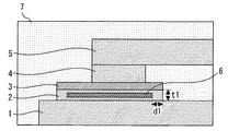
図1は、実施の形態1に係る半導体装置を示す断面図である。本実施の形態に係る半導体装置は、例えば自動車動力用モータを駆動する電源に用いられる。電極基板1の上面に第1のはんだ2を介して半導体チップ3が接合されている。半導体チップ3の上面に第2のはんだ4を介してリードフレーム5が接合されている。
FIG. 1 is a cross-sectional view showing a semiconductor device according to the first embodiment. The semiconductor device according to this embodiment is used, for example, as a power source for driving an automobile power motor. The
半導体チップ3は、例えばシリコンによって形成されたIGBT又はMOSFETなどのスイッチング半導体素子、又はDiodeなどの還流用半導体素子である。半導体チップ3の厚みは、耐圧クラスに応じて最適化される。例えば、ハイブリッド自動車又は電機自動車に用いられることが多いリチウムイオンバッテリーの電圧を考慮すると、半導体チップ3の耐圧クラスは600Vから800Vが望ましい。電気的特性のうち、特にDC損失を改善するためには、半導体チップ3の厚みは100μm以下が望ましい。
The
電極基板1は、例えば絶縁基板上に圧延又は鋳造で板状に形成されている。なお、絶縁基板の下面には導体基板が設けられ、その導体基板には複数の冷却用突起が設けられている。導体基板と複数の冷却用突起に直接冷却水を当てることで、半導体チップ3から発生する熱を効率的に冷やすことができる。電極基板1、導体基板及び複数の冷却用突起は、アルミ鋳造で絶縁基板を鋳包むことで一体形成することができる。電極基板1等の主な材料はアルミである。これにより、電気的・熱的伝導性を維持しつつ、冷却水に対する耐蝕性を確保し、コスト及び重量を抑えることができる。また、熱伝導を改善するためには、99%以上の高純度のアルミが望ましい。
The
第1及び第2のはんだ2,4は、例えばSn−Cu系、Sn−Ag系、又はSn−Ag−Cu系の鉛フリーはんだである。これにより、半導体チップ3をリードフレーム5又は電極基板1に還元雰囲気中で容易に電気的・熱的に接合することができる。そして、第1及び第2のはんだ2,4は、半導体チップ3の使用温度範囲200℃以下においても、固相状態を保つことができる。
The first and
リードフレーム5の主な材料は例えば銅である。リードフレーム5は、例えばCu材を圧延してCu板材を形成した後、打ち抜き加工で任意の形状に加工される。リードフレーム5は第2のはんだ4と電気的に接続される。
The main material of the
なお、半導体チップ3の上面と下面にそれぞれNiを含む材料からなるはんだ接合用金属膜が電解めっき法、スパッタ、又は蒸着などの気相堆積法により形成されている。上面と下面のはんだ接合用金属膜はそれぞれ第1及び第2のはんだ2,4に電気的・熱的に接続される。
A metal film for solder bonding made of a material containing Ni is formed on the upper surface and the lower surface of the
電極基板1と半導体チップ3との間において第1のはんだ2中に中間板6が設けられている。中間板6の主な材料は銅である。中間板6は、例えばCu材を圧延してCu板材を形成した後、打ち抜き加工で任意の形状に加工される。
An
電極基板1の上面、第1のはんだ2、半導体チップ3、第2のはんだ4、中間板6、リードフレーム5の一部は封止材7で覆われている。封止材7としてトランスファモールド樹脂又はポッティングレジンを用いることができる。封止材7が半導体チップ3に直接的に接している部分では半導体チップ3の変形を抑制することができる。
A part of the upper surface of the
続いて、本実施の形態に係る半導体装置の製造方法を説明する。まず、電極基板1上に中間板6、第1のはんだ2、半導体チップ3を順番に積層する。次に、第1のはんだ2を還元雰囲気中で加熱して溶融させ、第1のはんだ2及び中間板6を介して半導体チップ3の下面を電極基板1の上面に電気的・熱的に接合させる。熱的な接合を最大限得るために、半導体チップ3の下面のほぼ全面を接合させることが望ましい。また、第1のはんだ2に空気が巻き込まれてボイドが発生するのを防止するため、減圧下で第1のはんだ2を溶融させた後に復圧することで、第1のはんだ2から空気を排出することが望ましい。中間板6と第1のはんだ2を積層する順番は逆でもよいが、半導体チップ3の直下に中間板6を配置する場合、中間板6の打ち抜き加工のかえりが第1のはんだ2側に向くように配置することで半導体チップ3が傷つくのを防止して歩留まりを向上することができる。
Subsequently, a method of manufacturing the semiconductor device according to the present embodiment will be described. First, the
次に、リードフレーム5を半導体チップ3の上面に第2のはんだ4を用いて電気的に接続する。ここで、半導体チップ3の上面は熱的にリードフレーム5と接合する必要はない。また、半導体チップ3の端部とリードフレーム5との延面距離を確保する必要がある。そして、半導体チップ3の上面の信号端子と外部電極とを導体ワイヤなどを用いて接続する必要がある。そこで、リードフレーム5は半導体チップ3の上面に部分的に接合する。次に、電極基板1の上面、第1のはんだ2、半導体チップ3、第2のはんだ4、中間板6、リードフレーム5の少なくとも一部を封止材7で覆う。以上の工程により本実施の形態に係る半導体装置が製造される。
Next, the
図2は、電極基板と第1及び第2のはんだと中間板の耐力の温度依存性を示す図である。ここで、耐力とは、0.2%耐力のことを示し、降伏現象を示さない多くの金属材料において除荷した時に0.2%の塑性ひずみを生じさせる応力のことである。電極基板1の耐力と第1及び第2のはんだ2,4の耐力の大小関係が半導体装置の使用温度範囲において逆転する点が存在する。従って、第1のはんだ2と電極基板1にそれぞれ異なる温度域で変形が発生する。例えば、第1のはんだ2が変形する時には電極基板1が変形し難く、電極基板1が変形する時には第1のはんだ2が変形し難い。このため、それぞれの材料は元の位置に戻らず変形量が蓄積され、冷熱サイクルが繰り返されることで、変形量が大きくなっていく。
FIG. 2 is a diagram showing the temperature dependence of the yield strength of the electrode substrate, the first and second solders, and the intermediate plate. Here, the proof stress indicates a proof stress of 0.2%, and is a stress that causes a plastic strain of 0.2% when unloading in many metal materials that do not exhibit a yield phenomenon. There is a point where the magnitude relationship between the proof stress of the
そこで、本実施の形態では電極基板1と半導体チップ3との間において第1のはんだ2中に中間板6を設けている。そして、中間板6の耐力は、半導体装置の使用温度範囲の全てにおいて電極基板1及び第1のはんだ2の耐力よりも大きい。従って、電極基板1及び第1のはんだ2が冷熱サイクルで変形しても、中間板6は変形しないため、半導体チップ3の変形を抑制できる。特に、第2のはんだ4の直下は半導体チップ3が封止材7と直接的に接していないため、封止材7の固定力が及ばず冷熱サイクル及びパワーサイクルの応力で第2のはんだ4が変形したとき、拘束力を失い、変形しやすくなる。これに対して、半導体チップ3の下に変形し難い中間板6が設けられているため、半導体チップ3の変形を抑制することができる。この結果、冷熱サイクル及びパワーサイクルに対する信頼性を向上することができる。なお、本実施の形態では第1及び第2のはんだ2,4は同一の材料であるが、別の材料であっても上記の耐力関係を有していれば同様の効果が得られる。
Therefore, in the present embodiment, the
また、シリコンカーバイドなどの高温対応半導体チップを用いる場合、使用温度範囲は高温側は200℃まで拡大される。また、自動車用途では低温側は−55℃まで拡大される。このため、電極基板1と第1のはんだ2の変形量は大きくなりやすく、中間板6によって半導体チップ3の変形を抑制する必要がある。
Further, when a high temperature semiconductor chip such as silicon carbide is used, the operating temperature range is expanded to 200 ° C. on the high temperature side. In addition, the temperature on the low temperature side is expanded to -55 ° C for automobile applications. Therefore, the amount of deformation of the
また、中間板6と第1のはんだ2の線膨脹係数が異なることに起因して冷熱サイクルによる応力が発生する。この応力は半導体チップ3の端部で最大となる。第1のはんだ2を中間板6で分断してしまうと、半導体チップ3の端部における、第1のはんだ2の厚みが薄くなり、応力が大きくなる。特に、中間板6が第1のはんだ2中で傾いた場合、第1のはんだ2の端部の厚みは部分的に更に薄くなり、顕著に応力が増加する。そこで、中間板6を半導体チップ3及び第1のはんだ2より小さくし、平面視において半導体チップ3及び第1のはんだ2の内側に配置する。これにより、第1のはんだ2に中間板6を完全に埋没させることができ、第1のはんだ2の端部で中間板6によって第1のはんだ2が分断されるのを防ぐことができる。この結果、冷熱サイクルに対する信頼性を更に向上することができる。
Further, stress due to the thermal cycle is generated due to the difference in the linear expansion coefficients of the
また、中間板6の端部を半導体チップ3の端部から内側に後退させ、第1のはんだ2から中間板6を露出させないようにする。具体的には、半導体チップ3の端部と中間板6の端部との間隔d1が第1のはんだ2の厚みt1より大きくなるようにする。これにより、中間板6が第1のはんだ2中で傾いた場合も、半導体チップ3の端部で第1のはんだ2の厚みが薄くなることがなく、安定した信頼性を発揮することができる。
Further, the end portion of the
また、第2のはんだ4は、平面視において中間板6の内側に配置されている。パワーサイクルの応力により第2のはんだ4が変形すると、半導体チップ3が変形してしまう。そこで、中間板6により支持することで半導体チップ3の変形を抑えることができる。
Further, the
実施の形態2.
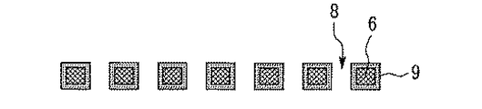
図3は、実施の形態2に係る中間板を示す平面図である。図4は、図3のI−IIに沿った断面図である。本実施の形態は、中間板6の構成以外は実施の形態1と同様である。
FIG. 3 is a plan view showing an intermediate plate according to the second embodiment. FIG. 4 is a cross-sectional view taken along the line I-II of FIG. The present embodiment is the same as that of the first embodiment except for the configuration of the
中間板6に、例えば打ち抜き加工により、複数の貫通孔8が設けられている。これにより、第1のはんだ2が貫通孔8を通って上下両面に濡れ広がることができるため、中間板6の上面側と下面側の両方に第1のはんだ2を置く必要が無い。従って、第1のはんだ2の部材点数と組み立て作業を削減でき、製造コストを低減することができる。
The
また、めっき膜9が中間板6の表面を覆っている。めっき膜9の主な材料はニッケルであり、めっき膜9は中間板6よりも第1のはんだ2に対する濡れ性が高い。これにより、はんだ濡れ性を向上することができるので、ボイド不良率を低減でき、製造ロスコストを低減することができる。
Further, the
また、めっき膜9は貫通孔8を打ち抜き加工した後に形成されるため、複数の貫通孔8の側壁にも形成されている。これにより、第1のはんだ2が貫通孔8の側壁にも濡れ広がって貫通孔8の内側に充填されるため、ボイドの発生を抑制し、信頼性を向上することができる。
Further, since the
また、貫通孔8の大きさは500μmΦ以下であることが好ましい。複数の貫通孔8に空気を巻き込むと第1のはんだ2中にボイドが形成されるが、ボイド径が500μm以下では熱的な悪影響が少なく、熱抵抗の悪化及び短絡耐量の低下は発生し難い。また、500μmΦを超える空気が複数の貫通孔8に巻き込まれた場合、第1のはんだ2の表面張力によって、空隙が複数の貫通孔8に細分化されるため、500μmΦを超えるボイドが発生し難く、製造歩留まりを向上することができる。
Further, the size of the through
また、第1のはんだ2とめっき膜9との間で金属間化合物が形成される。この金属間化合物上で冷熱サイクルによりカーケンダルボイドが発生するため、はんだクラックに繋がることがある。従って、実施の形態1と同様に第1のはんだ2から中間板6を露出させないことが望ましい。
Further, an intermetallic compound is formed between the
実施の形態3.
図5は、実施の形態3に係る半導体装置を示す断面図である。電極基板1と半導体チップ3の端部との間に、アルミワイヤなどにより複数のバンプ10が設けられている。バンプによって半導体チップ3と電極基板1との距離を確保することができるため、半導体チップ3が傾いて実装されて第1のはんだ2が部分的に薄くなるのを防ぐことができる。
FIG. 5 is a cross-sectional view showing the semiconductor device according to the third embodiment. A plurality of
また、中間板6は、平面視において複数のバンプ10の内側に配置されている。これにより、はんだ接合工程中の中間板6の動きがバンプ10により制限されることで、中間板6が半導体チップ3より外側に流れて第1のはんだ2から露出するのを防止できる。
Further, the
また、中間板6の厚みt2はバンプの高さh1より薄い。これにより、はんだ接合工程で、中間板6が溶融状態の第1のはんだ2中で傾いたとしても、バンプ10により半導体チップ3の高さを維持することができる。
Further, the thickness t2 of the
なお、実施の形態1〜3において、半導体チップ3の厚みが100μm以下である場合、半導体チップ3の損失を低減することができるが、周辺部材の変形につられて半導体チップ3が変形し易くなる。このため、中間板6を設けて信頼性の低下を防ぐ必要性が高い。
In the first to third embodiments, when the thickness of the
また、中間板6の主な材料はモリブデンでもよい。この場合、例えばモリブデン材を圧延してモリブデン板材を形成した後、打ち抜き加工で任意の形状に加工することで中間板6が形成される。モリブデンを用いることで中間板6の線膨脹係数を半導体チップ3の主な材料であるシリコンに近づけることができるため、両者の熱膨張係数差により発生する応力を低減することができる。従って、熱サイクル又はパワーサイクルにより半導体チップ3に加わるストレスを更に軽減できるため、電気的・熱的伝導性を維持しつつ信頼性を更に向上することができる。
Further, the main material of the
また、半導体チップ3に化合物半導体を用いることで高温まで使用することができる。特に主な材料としてカーボンを有するSiCなどの化合物半導体を用いることで更に高温まで使用することができる。また、シリコンに比べてバンドギャップが大きいワイドバンドギャップ半導体によって形成された半導体チップ3は、耐電圧性や許容電流密度が高いため、小型化できる。この小型化された半導体チップ3を用いることで、この半導体チップ3を組み込んだ半導体装置も小型化できる。また、半導体チップ3の耐熱性が高いため、ヒートシンクの放熱フィンを小型化でき、水冷部を空冷化できるので、半導体装置を更に小型化できる。また、半導体チップ3の電力損失が低く高効率であるため、半導体装置を高効率化できる。ワイドバンドギャップ半導体は、SiCの他にも、例えば窒化ガリウム系材料又はダイヤモンドである。
Further, by using a compound semiconductor for the
1 電極基板、2 第1のはんだ、3 半導体チップ、4 第2のはんだ、5 リードフレーム、6 中間板、9 めっき膜、8 貫通孔、10 バンプ 1 Electrode board, 2 1st solder, 3 Semiconductor chip, 4 2nd solder, 5 Lead frame, 6 Intermediate plate, 9 Plating film, 8 Through hole, 10 Bump
Claims (17)
前記電極基板の上面に第1のはんだを介して接合された半導体チップと、
前記半導体チップの上面に第2のはんだを介して接合されたリードフレームと、
前記電極基板と前記半導体チップとの間において前記第1のはんだ中に設けられた中間板と、
前記電極基板と前記半導体チップとの間に設けられた複数のバンプとを備え、
前記中間板の耐力は、半導体装置の使用温度範囲の全てにおいて前記電極基板及び前記第1のはんだの耐力よりも大きく、
前記中間板は、平面視において前記複数のバンプの内側に配置されていることを特徴とする半導体装置。 With the electrode substrate
A semiconductor chip bonded to the upper surface of the electrode substrate via a first solder,
A lead frame bonded to the upper surface of the semiconductor chip via a second solder,
An intermediate plate provided in the first solder between the electrode substrate and the semiconductor chip,
A plurality of bumps provided between the electrode substrate and the semiconductor chip are provided.
The proof stress of the intermediate plate is larger than the proof stress of the electrode substrate and the first solder in the entire operating temperature range of the semiconductor device.
A semiconductor device characterized in that the intermediate plate is arranged inside the plurality of bumps in a plan view.
前記電極基板の上面に第1のはんだを介して接合された半導体チップと、
前記半導体チップの上面に第2のはんだを介して接合されたリードフレームと、
前記電極基板と前記半導体チップとの間において前記第1のはんだ中に設けられた中間板とを備え、
前記中間板の耐力は、半導体装置の使用温度範囲の全てにおいて前記電極基板及び前記第1のはんだの耐力よりも大きく、
前記中間板の主な材料は銅であることを特徴とする半導体装置。 With the electrode substrate
A semiconductor chip bonded to the upper surface of the electrode substrate via a first solder,
A lead frame bonded to the upper surface of the semiconductor chip via a second solder,
An intermediate plate provided in the first solder is provided between the electrode substrate and the semiconductor chip.
The proof stress of the intermediate plate is larger than the proof stress of the electrode substrate and the first solder in the entire operating temperature range of the semiconductor device.
A semiconductor device characterized in that the main material of the intermediate plate is copper.
前記めっき膜は前記複数の貫通孔の側壁にも形成されていることを特徴とする請求項8又は9に記載の半導体装置。 The intermediate plate is provided with a plurality of through holes.
The semiconductor device according to claim 8 or 9 , wherein the plating film is also formed on the side walls of the plurality of through holes.
Applications Claiming Priority (1)
| Application Number | Priority Date | Filing Date | Title |
|---|---|---|---|
| PCT/JP2016/072158 WO2018020640A1 (en) | 2016-07-28 | 2016-07-28 | Semiconductor device |
Publications (2)
| Publication Number | Publication Date |
|---|---|
| JPWO2018020640A1 JPWO2018020640A1 (en) | 2018-12-13 |
| JP6777148B2 true JP6777148B2 (en) | 2020-10-28 |
Family
ID=61016579
Family Applications (1)
| Application Number | Title | Priority Date | Filing Date |
|---|---|---|---|
| JP2018530284A Active JP6777148B2 (en) | 2016-07-28 | 2016-07-28 | Semiconductor device |
Country Status (5)
| Country | Link |
|---|---|
| US (1) | US12009332B2 (en) |
| JP (1) | JP6777148B2 (en) |
| CN (1) | CN109478543B (en) |
| DE (1) | DE112016007096B4 (en) |
| WO (1) | WO2018020640A1 (en) |
Families Citing this family (4)
| Publication number | Priority date | Publication date | Assignee | Title |
|---|---|---|---|---|
| WO2020213167A1 (en) * | 2019-04-19 | 2020-10-22 | 三菱電機株式会社 | Semiconductor device, and manufacturing method for same |
| US20230146579A1 (en) * | 2019-10-23 | 2023-05-11 | Alpha Assembly Solutions Inc. | Engineered materials for electronics assembly |
| JP7543655B2 (en) * | 2020-02-14 | 2024-09-03 | 富士電機株式会社 | Semiconductor Module |
| CN114743947B (en) * | 2022-04-11 | 2023-09-19 | 中国工程物理研究院电子工程研究所 | TO-form-based power device packaging structure and packaging method |
Family Cites Families (41)
| Publication number | Priority date | Publication date | Assignee | Title |
|---|---|---|---|---|
| JPS5665650U (en) * | 1979-10-23 | 1981-06-01 | ||
| JPS56172938U (en) * | 1980-05-23 | 1981-12-21 | ||
| EP0229850B1 (en) * | 1985-07-16 | 1992-06-10 | Nippon Telegraph and Telephone Corporation | Connection terminals between substrates and method of producing the same |
| JPS63251127A (en) * | 1987-04-06 | 1988-10-18 | Ngk Insulators Ltd | Combined construction of members with different thermal expansion and combining method thereof |
| US5188280A (en) * | 1989-04-28 | 1993-02-23 | Hitachi Ltd. | Method of bonding metals, and method and apparatus for producing semiconductor integrated circuit device using said method of bonding metals |
| EP0568313A2 (en) * | 1992-05-01 | 1993-11-03 | Nippon CMK Corp. | A method of manufacturing a multilayer printed wiring board |
| JP2989406B2 (en) * | 1993-01-29 | 1999-12-13 | シャープ株式会社 | Preplated frame for semiconductor device and method of manufacturing the same |
| US6070321A (en) * | 1997-07-09 | 2000-06-06 | International Business Machines Corporation | Solder disc connection |
| US6158644A (en) * | 1998-04-30 | 2000-12-12 | International Business Machines Corporation | Method for enhancing fatigue life of ball grid arrays |
| JP2000332369A (en) * | 1999-05-25 | 2000-11-30 | Mitsui Mining & Smelting Co Ltd | Printed-circuit board and its manufacture |
| US6197618B1 (en) * | 2000-05-04 | 2001-03-06 | General Semiconductor Ireland | Semiconductor device fabrication using adhesives |
| TW524030B (en) * | 2000-10-02 | 2003-03-11 | Matsushita Electric Ind Co Ltd | Card-type recording medium and its manufacture method |
| JP2002203942A (en) * | 2000-12-28 | 2002-07-19 | Fuji Electric Co Ltd | Power semiconductor module |
| US20040078964A1 (en) * | 2001-03-07 | 2004-04-29 | Kazuhiro Itou | Land portion of printed wiring board, method for manufacturing printed wiring board, and printed wiring board mounting method |
| JP4848539B2 (en) * | 2001-08-23 | 2011-12-28 | Dowaメタルテック株式会社 | Heat sink, power semiconductor module, IC package |
| US6821667B2 (en) * | 2001-10-01 | 2004-11-23 | Delphi Technologies, Inc. | Fuel cell stack having foil interconnects and laminated spacers |
| JP2003133337A (en) | 2001-10-23 | 2003-05-09 | Nissan Motor Co Ltd | Semiconductor-mounting structure and semiconductor mounting method |
| US7532481B2 (en) * | 2004-04-05 | 2009-05-12 | Mitsubishi Materials Corporation | Al/AlN joint material, base plate for power module, power module, and manufacturing method of Al/AlN joint material |
| JP5491682B2 (en) * | 2004-08-13 | 2014-05-14 | 日立金属株式会社 | Flat conductor for solar cell, method for manufacturing the same, and lead wire for solar cell |
| JP4343117B2 (en) * | 2005-01-07 | 2009-10-14 | 株式会社ルネサステクノロジ | Semiconductor device and manufacturing method thereof |
| JP4421528B2 (en) * | 2005-07-28 | 2010-02-24 | シャープ株式会社 | Solder mounting structure, manufacturing method thereof, and use thereof |
| JP4569423B2 (en) * | 2005-08-31 | 2010-10-27 | 株式会社日立製作所 | Manufacturing method of semiconductor device |
| JP2007157863A (en) * | 2005-12-02 | 2007-06-21 | Hitachi Ltd | Power semiconductor device, and method of manufacturing same |
| US20090186195A1 (en) * | 2006-09-08 | 2009-07-23 | Reactive Nanotechnologies, Inc. | Reactive Multilayer Joining With Improved Metallization Techniques |
| JP2008098607A (en) * | 2006-09-13 | 2008-04-24 | Hitachi Cable Ltd | Connection lead wire for solar cell, its production process and solar cell |
| JP5272191B2 (en) * | 2007-08-31 | 2013-08-28 | 三菱電機株式会社 | Semiconductor device and manufacturing method of semiconductor device |
| JP2009224560A (en) * | 2008-03-17 | 2009-10-01 | Denso Corp | Semiconductor device and production method therefor |
| JP5241344B2 (en) | 2008-06-30 | 2013-07-17 | 日立オートモティブシステムズ株式会社 | Power module and power converter |
| WO2012073306A1 (en) | 2010-11-29 | 2012-06-07 | トヨタ自動車株式会社 | Power module |
| JP5325917B2 (en) * | 2011-03-17 | 2013-10-23 | 株式会社東芝 | Semiconductor device and manufacturing method thereof |
| JP2013113638A (en) | 2011-11-25 | 2013-06-10 | Toyota Motor Corp | Semiconductor device |
| KR102007780B1 (en) * | 2012-07-31 | 2019-10-21 | 삼성전자주식회사 | Methods for fabricating semiconductor devices having multi-bump structural electrical interconnections |
| JP2014041876A (en) | 2012-08-21 | 2014-03-06 | Mitsubishi Electric Corp | Power semiconductor device |
| JP5686128B2 (en) * | 2012-11-29 | 2015-03-18 | トヨタ自動車株式会社 | Semiconductor device |
| US8896118B2 (en) * | 2013-03-13 | 2014-11-25 | Texas Instruments Incorporated | Electronic assembly with copper pillar attach substrate |
| US11239123B2 (en) * | 2013-08-29 | 2022-02-01 | Mitsubishi Electric Corporation | Semiconductor module, semiconductor device, and vehicle |
| JP6399738B2 (en) | 2013-09-25 | 2018-10-03 | 富士電機株式会社 | Semiconductor device |
| JP2016046403A (en) * | 2014-08-25 | 2016-04-04 | トヨタ自動車株式会社 | Semiconductor device |
| CN105575924B (en) * | 2014-10-15 | 2018-07-03 | 台达电子工业股份有限公司 | Power module |
| US9633957B2 (en) * | 2014-11-28 | 2017-04-25 | Infineon Technologies Ag | Semiconductor device, a power semiconductor device, and a method for processing a semiconductor device |
| KR102430984B1 (en) * | 2015-09-22 | 2022-08-09 | 삼성전자주식회사 | Semiconductor device and method of manufacturing the same |
-
2016
- 2016-07-28 CN CN201680087903.5A patent/CN109478543B/en active Active
- 2016-07-28 DE DE112016007096.9T patent/DE112016007096B4/en active Active
- 2016-07-28 JP JP2018530284A patent/JP6777148B2/en active Active
- 2016-07-28 US US16/088,455 patent/US12009332B2/en active Active
- 2016-07-28 WO PCT/JP2016/072158 patent/WO2018020640A1/en active Application Filing
Also Published As
| Publication number | Publication date |
|---|---|
| DE112016007096B4 (en) | 2023-06-29 |
| CN109478543B (en) | 2022-07-05 |
| US20190157235A1 (en) | 2019-05-23 |
| JPWO2018020640A1 (en) | 2018-12-13 |
| CN109478543A (en) | 2019-03-15 |
| US12009332B2 (en) | 2024-06-11 |
| WO2018020640A1 (en) | 2018-02-01 |
| DE112016007096T5 (en) | 2019-04-18 |
Similar Documents
| Publication | Publication Date | Title |
|---|---|---|
| US10727163B2 (en) | Semiconductor device | |
| JP5572678B2 (en) | Semiconductor device including a clad base plate | |
| JP6272512B2 (en) | Semiconductor device and manufacturing method of semiconductor device | |
| JP4569473B2 (en) | Resin-encapsulated power semiconductor module | |
| JP6199397B2 (en) | Semiconductor device and manufacturing method thereof | |
| US10461012B2 (en) | Semiconductor module with reinforcing board | |
| JP6777148B2 (en) | Semiconductor device | |
| WO2007145303A1 (en) | Semiconductor module and method for manufacturing same | |
| US10879209B2 (en) | Encapsulated stress mitigation layer and power electronic assemblies incorporating the same | |
| WO2011040313A1 (en) | Semiconductor module, process for production thereof | |
| US10475721B2 (en) | Power semiconductor device and method for manufacturing same | |
| JP6945418B2 (en) | Semiconductor devices and manufacturing methods for semiconductor devices | |
| JP5899952B2 (en) | Semiconductor module | |
| JP6182850B2 (en) | Power converter | |
| JP5100674B2 (en) | Inverter device | |
| JP7147186B2 (en) | semiconductor equipment | |
| JP2015002305A (en) | Semiconductor device | |
| KR102684858B1 (en) | Heat emitting post bonded semiconductor package and method of fabricating the same | |
| JP2011176087A (en) | Semiconductor module, and power conversion apparatus | |
| WO2023136264A1 (en) | Resin-sealed semiconductor apparatus | |
| Barlow et al. | High-temperature high-power packaging techniques for HEV traction applications | |
| JP2023141693A (en) | Semiconductor device | |
| JP2024013570A (en) | Semiconductor device, method for manufacturing semiconductor device, and power converter | |
| JP2023162108A (en) | Resin-encapsulated semiconductor devices and power conversion device | |
| JP2014120717A (en) | Electronic device and manufacturing method of the same |
Legal Events
| Date | Code | Title | Description |
|---|---|---|---|
| A621 | Written request for application examination |
Free format text: JAPANESE INTERMEDIATE CODE: A621 Effective date: 20180816 |
|
| A131 | Notification of reasons for refusal |
Free format text: JAPANESE INTERMEDIATE CODE: A131 Effective date: 20191023 |
|
| A521 | Request for written amendment filed |
Free format text: JAPANESE INTERMEDIATE CODE: A523 Effective date: 20191119 |
|
| A131 | Notification of reasons for refusal |
Free format text: JAPANESE INTERMEDIATE CODE: A131 Effective date: 20200526 |
|
| A521 | Request for written amendment filed |
Free format text: JAPANESE INTERMEDIATE CODE: A523 Effective date: 20200617 |
|
| TRDD | Decision of grant or rejection written | ||
| A01 | Written decision to grant a patent or to grant a registration (utility model) |
Free format text: JAPANESE INTERMEDIATE CODE: A01 Effective date: 20200908 |
|
| A61 | First payment of annual fees (during grant procedure) |
Free format text: JAPANESE INTERMEDIATE CODE: A61 Effective date: 20200921 |
|
| R150 | Certificate of patent or registration of utility model |
Ref document number: 6777148 Country of ref document: JP Free format text: JAPANESE INTERMEDIATE CODE: R150 |
|
| R250 | Receipt of annual fees |
Free format text: JAPANESE INTERMEDIATE CODE: R250 |
|
| R250 | Receipt of annual fees |
Free format text: JAPANESE INTERMEDIATE CODE: R250 |