JP6762024B2 - Laser processing equipment and laser processing method - Google Patents
Laser processing equipment and laser processing method Download PDFInfo
- Publication number
- JP6762024B2 JP6762024B2 JP2016148327A JP2016148327A JP6762024B2 JP 6762024 B2 JP6762024 B2 JP 6762024B2 JP 2016148327 A JP2016148327 A JP 2016148327A JP 2016148327 A JP2016148327 A JP 2016148327A JP 6762024 B2 JP6762024 B2 JP 6762024B2
- Authority
- JP
- Japan
- Prior art keywords
- resin layer
- laser
- resin
- layer
- cut
- Prior art date
- Legal status (The legal status is an assumption and is not a legal conclusion. Google has not performed a legal analysis and makes no representation as to the accuracy of the status listed.)
- Active
Links
Images


Classifications
-
- B—PERFORMING OPERATIONS; TRANSPORTING
- B23—MACHINE TOOLS; METAL-WORKING NOT OTHERWISE PROVIDED FOR
- B23K—SOLDERING OR UNSOLDERING; WELDING; CLADDING OR PLATING BY SOLDERING OR WELDING; CUTTING BY APPLYING HEAT LOCALLY, e.g. FLAME CUTTING; WORKING BY LASER BEAM
- B23K26/00—Working by laser beam, e.g. welding, cutting or boring
- B23K26/36—Removing material
- B23K26/38—Removing material by boring or cutting
-
- B—PERFORMING OPERATIONS; TRANSPORTING
- B23—MACHINE TOOLS; METAL-WORKING NOT OTHERWISE PROVIDED FOR
- B23K—SOLDERING OR UNSOLDERING; WELDING; CLADDING OR PLATING BY SOLDERING OR WELDING; CUTTING BY APPLYING HEAT LOCALLY, e.g. FLAME CUTTING; WORKING BY LASER BEAM
- B23K26/00—Working by laser beam, e.g. welding, cutting or boring
- B23K26/0006—Working by laser beam, e.g. welding, cutting or boring taking account of the properties of the material involved
-
- B—PERFORMING OPERATIONS; TRANSPORTING
- B23—MACHINE TOOLS; METAL-WORKING NOT OTHERWISE PROVIDED FOR
- B23K—SOLDERING OR UNSOLDERING; WELDING; CLADDING OR PLATING BY SOLDERING OR WELDING; CUTTING BY APPLYING HEAT LOCALLY, e.g. FLAME CUTTING; WORKING BY LASER BEAM
- B23K26/00—Working by laser beam, e.g. welding, cutting or boring
- B23K26/36—Removing material
- B23K26/40—Removing material taking account of the properties of the material involved
- B23K26/402—Removing material taking account of the properties of the material involved involving non-metallic material, e.g. isolators
-
- B—PERFORMING OPERATIONS; TRANSPORTING
- B23—MACHINE TOOLS; METAL-WORKING NOT OTHERWISE PROVIDED FOR
- B23K—SOLDERING OR UNSOLDERING; WELDING; CLADDING OR PLATING BY SOLDERING OR WELDING; CUTTING BY APPLYING HEAT LOCALLY, e.g. FLAME CUTTING; WORKING BY LASER BEAM
- B23K2103/00—Materials to be soldered, welded or cut
- B23K2103/16—Composite materials, e.g. fibre reinforced
- B23K2103/166—Multilayered materials
-
- B—PERFORMING OPERATIONS; TRANSPORTING
- B23—MACHINE TOOLS; METAL-WORKING NOT OTHERWISE PROVIDED FOR
- B23K—SOLDERING OR UNSOLDERING; WELDING; CLADDING OR PLATING BY SOLDERING OR WELDING; CUTTING BY APPLYING HEAT LOCALLY, e.g. FLAME CUTTING; WORKING BY LASER BEAM
- B23K2103/00—Materials to be soldered, welded or cut
- B23K2103/30—Organic material
- B23K2103/42—Plastics
Description
本発明は、レーザ加工装置及びレーザ加工方法、特に、レーザ光を照射することで樹脂基板を切断する装置及び方法に関する。 The present invention relates to a laser processing apparatus and a laser processing method, particularly an apparatus and a method for cutting a resin substrate by irradiating a laser beam.
樹脂基板の種類は、単層樹脂基板と、複層樹脂基板とに分かれる。複層樹脂基板は、異なる材料の複数の樹脂層を含む。また、製品によって機能性膜(無機・金属・有機)を積層することがある。
複層樹脂基板を切断する装置として、レーザ加工装置が用いられる(例えば、特許文献1を参照)。複層樹脂基板は、レーザ加工装置によって、上側の層だけが切断されたり(ハーフカット加工)、全ての層が切断されたりする(フルカット加工)。
The types of resin substrates are divided into single-layer resin substrates and multi-layer resin substrates. The multi-layer resin substrate contains a plurality of resin layers of different materials. In addition, functional films (inorganic, metal, organic) may be laminated depending on the product.
A laser processing apparatus is used as an apparatus for cutting the multilayer resin substrate (see, for example, Patent Document 1). In the multi-layer resin substrate, only the upper layer is cut (half-cut processing) or all the layers are cut by the laser processing device (full-cut processing).
複層樹脂基板をフルカット加工するときに、表面層より下側の層(例えば、中間層)がレーザ光に対して吸収率の高い材料からなる場合は、表面層より先に中間層が加工されることがある。この場合は、表面層の内側で発生したデブリが表面層によって排出を妨げられる。そのため、デブリが、樹脂層の境界に進入したり、内部に堆積したり、発熱して周辺部分を変質したりする。 When the multi-layer resin substrate is fully cut, if the layer below the surface layer (for example, the intermediate layer) is made of a material having a high absorption rate for laser light, the intermediate layer is processed before the surface layer. May be done. In this case, the debris generated inside the surface layer is prevented from being discharged by the surface layer. Therefore, debris invades the boundary of the resin layer, accumulates inside, or generates heat to deteriorate the peripheral portion.
本発明の目的は、レーザ加工装置によって複層樹脂基板をフルカット加工する際に、表面側の層の加工時に内側の樹脂層が加工されにくくすることにある。 An object of the present invention is to make it difficult for the inner resin layer to be processed when the surface side layer is processed when the multi-layer resin substrate is fully cut by the laser processing apparatus.
以下に、課題を解決するための手段として複数の態様を説明する。これら態様は、必要に応じて任意に組み合せることができる。 Hereinafter, a plurality of aspects will be described as means for solving the problem. These aspects can be arbitrarily combined as needed.
本発明の一見地に係るレーザ加工装置は、表面側から第1樹脂層と第2樹脂層とを有する複層樹脂基板を切断するための装置であって、第1レーザ装置と、第2レーザ装置とを備えている。
第1レーザ装置は、第1樹脂層を切断するための第1レーザ光を発生する装置である。第1レーザ光は、第1樹脂層に対するよりも第2樹脂層に対して吸収率が低い。
第2レーザ装置は、第2樹脂層を切断するための第2レーザ光を発生する装置である。第2レーザ光は、第1樹脂層に対するよりも第2樹脂層に対して吸収率が高い。
The laser processing apparatus according to the first aspect of the present invention is an apparatus for cutting a multi-layer resin substrate having a first resin layer and a second resin layer from the surface side, and is a first laser apparatus and a second laser. It is equipped with a device.
The first laser device is a device that generates a first laser beam for cutting the first resin layer. The first laser beam has a lower absorption rate with respect to the second resin layer than with respect to the first resin layer.
The second laser device is a device that generates a second laser beam for cutting the second resin layer. The second laser beam has a higher absorption rate with respect to the second resin layer than with respect to the first resin layer.
この装置では、第1レーザ光によって第1樹脂層が切断されるときに、第2樹脂層は加工されない条件(レーザパワー等)が選定される。なぜなら、第1レーザ光は第1樹脂層に対するよりも第2樹脂層に対して吸収率が低いからである。その結果、第1樹脂層の切断時に、第2樹脂層が加工されにくい。
第1樹脂層が切断された後に、第2レーザ光によって第2樹脂層が切断される。このときに発生するデブリは、第1樹脂層の切断部分から外部に出ていく。したがって、第2樹脂層加工時に発生するデブリが第1樹脂層内に止まることがない。
In this apparatus, when the first resin layer is cut by the first laser beam, a condition (laser power or the like) in which the second resin layer is not processed is selected. This is because the first laser beam has a lower absorption rate with respect to the second resin layer than with respect to the first resin layer. As a result, when the first resin layer is cut, the second resin layer is less likely to be processed.
After the first resin layer is cut, the second resin layer is cut by the second laser beam. The debris generated at this time goes out from the cut portion of the first resin layer. Therefore, the debris generated during the processing of the second resin layer does not stop in the first resin layer.
第1レーザ光の第2樹脂層に対する吸収率は30%以下、好ましくは20%以下であってもよい。 The absorption rate of the first laser beam with respect to the second resin layer may be 30% or less, preferably 20% or less.
第2レーザ光の第2樹脂層に対する吸収率は70%以上、好ましくは80%以上であってもよい。 The absorption rate of the second laser beam to the second resin layer may be 70% or more, preferably 80% or more.
第2樹脂層はPIを含み、第1レーザ装置はCO2レーザであり、第2レーザ装置はUVレーザであってもよい。 The second resin layer may contain PI, the first laser device may be a CO 2 laser, and the second laser device may be a UV laser.
本発明の他の見地に係るレーザ加工方法は、表面側から第1樹脂層と第2樹脂層とを有する複層樹脂基板を切断する方法であって、下記のステップを備えている。
◎第1樹脂層に対するよりも第2樹脂層に対して吸収率が低い第1レーザ光を発生することで、第1樹脂層を切断する第1切断ステップ
◎第1切断ステップの後に、第1樹脂層に対するよりも第2樹脂層に対して吸収率が高い第2レーザ光を発生して第1樹脂層の切断部分に照射することで、第2樹脂層を切断する第2切断ステップ
The laser processing method according to another aspect of the present invention is a method of cutting a multi-layer resin substrate having a first resin layer and a second resin layer from the surface side, and includes the following steps.
◎ First cutting step of cutting the first resin layer by generating a first laser beam having a lower absorption rate for the second resin layer than for the first resin layer ◎ After the first cutting step, the first A second cutting step of cutting the second resin layer by generating a second laser beam having a higher absorption rate for the second resin layer than for the resin layer and irradiating the cut portion of the first resin layer.
この方法では、第1レーザ光によって第1樹脂層が切断されるときに、第2樹脂層は加工されない。なぜなら、第1レーザ光は第1樹脂層に対するよりも第2樹脂層に対して吸収率が低いからである。その結果、第1樹脂層の切断時に、第2樹脂層の加工に起因する不具合が生じにくい。
第1樹脂層が切断された後に、第2レーザ光によって第2樹脂層が切断される。このときに発生するデブリは、第1樹脂層の切断部分から外部に出ていく。したがって、第2樹脂層加工時に発生するデブリが第1樹脂層内に止まることがない。
In this method, when the first resin layer is cut by the first laser beam, the second resin layer is not processed. This is because the first laser beam has a lower absorption rate with respect to the second resin layer than with respect to the first resin layer. As a result, when the first resin layer is cut, defects due to the processing of the second resin layer are less likely to occur.
After the first resin layer is cut, the second resin layer is cut by the second laser beam. The debris generated at this time goes out from the cut portion of the first resin layer. Therefore, the debris generated during the processing of the second resin layer does not stop in the first resin layer.
本発明に係るレーザ加工装置及びレーザ加工方法では、複層樹脂基板をフルカット加工する際に、表面側の樹脂層の加工時に内側の樹脂層が加工されにくい。 In the laser processing apparatus and the laser processing method according to the present invention, when the multi-layer resin substrate is fully cut, the inner resin layer is less likely to be processed when the surface side resin layer is processed.
1.第1実施形態
(1)全体構成
図1に、本発明の一実施形態による樹脂基板切断用のレーザ加工装置1の全体構成を示す。図1は、本発明の第1実施形態のレーザ加工装置の模式図である。
レーザ加工装置1は、樹脂基板Pをフルカット加工する装置である。樹脂基板とは、樹脂シート、樹脂フィルムともいわれるものである。
1. 1. First Embodiment (1) Overall Configuration FIG. 1 shows the overall configuration of the
The
レーザ加工装置1は、レーザ装置3を備えている。レーザ装置3は、樹脂基板Pにレーザ光を照射するための第1レーザ発振器9Aを有している。第1レーザ発振器9Aは、例えば、CO2レーザである。レーザ装置3は、樹脂基板Pにレーザ光を照射するための第2レーザ発振器9Bを有している。第2レーザ発振器9Bは、例えば、UVレーザである。
レーザ装置3は、レーザ光を後述する機械駆動系に伝送する伝送光学系11を有している。伝送光学系11は、例えば、図示しないが、集光レンズ、複数のミラー、プリズム、ビームエキスパンダ等を有する。また、伝送光学系11は、例えば、第1レーザ発振器9A、第2レーザ発振器9B及び他の光学系が組み込まれたレーザ照射ヘッド(図示せず)をX軸方向に移動させるためのX軸方向移動機構(図示せず)を有している。
伝送光学系11は、第1レーザ発振器9Aと第2レーザ発振器9Bでそれぞれ別の光学機構を有していてもよいし、共有の光学機構を切り換えて使用可能であってもよい。
The
The
The transmission
レーザ加工装置1は、機械駆動系5を備えている。機械駆動系5は、ベッド13と、樹脂基板Pが載置される加工テーブル15と、加工テーブル15をベッド13に対して水平方向に移動させる移動装置17とを有している。移動装置17は、ガイドレール、移動テーブル、モータ等を有する公知の機構である。
The
レーザ加工装置1は、制御部7を備えている。制御部7は、プロセッサ(例えば、CPU)と、記憶装置(例えば、ROM、RAM、HDD、SSDなど)と、各種インターフェース(例えば、A/Dコンバータ、D/Aコンバータ、通信インターフェースなど)を有するコンピュータシステムである。制御部7は、記憶部(記憶装置の記憶領域の一部又は全部に対応)に保存されたプログラムを実行することで、各種制御動作を行う。
制御部7は、単一のプロセッサで構成されていてもよいが、各制御のために独立した複数のプロセッサから構成されていてもよい。
The
The
制御部7には、図示しないが、樹脂基板Pの大きさ、形状及び位置を検出するセンサ、各装置の状態を検出するためのセンサ及びスイッチ、並びに情報入力装置が接続されている。
この実施形態では、制御部7は、第1レーザ発振器9A及び第2レーザ発振器9Bを制御できる。また、制御部7は、移動装置17を制御できる。さらに、制御部7は、伝送光学系11を制御できる。
Although not shown, the
In this embodiment, the
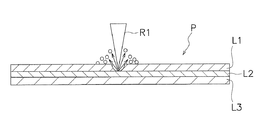
樹脂基板Pは、図3に示すように、複層の樹脂からなる複層樹脂基板である。図3は、樹脂基板の構造を示す模式的断面図である。具体的には、樹脂基板Pは、三層構造であり、表側から、第1樹脂層L1と、第2樹脂層L2と、第3樹脂層L3とを有している。
一例として、第1樹脂層L1は、PETを含む。第2樹脂層L2は、PIを含む。第3樹脂層L3は、PETを含む。
一例として、各樹脂層は接着層により互いに接着されている。
一例として、第2樹脂層L2の上面には、回路が形成されている。
As shown in FIG. 3, the resin substrate P is a multi-layer resin substrate made of a multi-layer resin. FIG. 3 is a schematic cross-sectional view showing the structure of the resin substrate. Specifically, the resin substrate P has a three-layer structure, and has a first resin layer L1, a second resin layer L2, and a third resin layer L3 from the front side.
As an example, the first resin layer L1 contains PET. The second resin layer L2 contains PI. The third resin layer L3 contains PET.
As an example, the resin layers are adhered to each other by an adhesive layer.
As an example, a circuit is formed on the upper surface of the second resin layer L2.
(2)動作
図2〜図4を用いて、レーザ光による樹脂基板Pの加工動作を説明する。図2は、フルカット加工の制御動作を示すフローチャートである。図4は、樹脂基板の加工状態を示す模式的断面図である。
制御部7が、レーザ発振器9を駆動して、樹脂基板Pの切断を実行する。以下、切断動作を具体的に説明する。
(2) Operation The processing operation of the resin substrate P by the laser beam will be described with reference to FIGS. 2 to 4. FIG. 2 is a flowchart showing a control operation of full-cut processing. FIG. 4 is a schematic cross-sectional view showing a processed state of the resin substrate.
The
ステップS1では、第1樹脂層L1を切断する。具体的には、制御部7は、第1レーザ発振器9Aを駆動することで、レーザ光を切断ラインCに沿って移動させる。図3に示すように、第1レーザ光R1によって、第1樹脂層L1が切断される。レーザ光の走査回数は1回でもよいし、複数回でもよい。
第1レーザ光R1によって第1樹脂層L1が切断されるときに、第2樹脂層L2は加工されない。なぜなら、第1レーザ光R1は、第1樹脂層L1に対するよりも第2樹脂層L2に対して吸収率が低いからである。その結果、第1樹脂層L1の切断時に、第2樹脂層L2の加工による不具合が生じにくい。
具体例として、CO2レーザのPIに対する吸収率は、9.4μ波長帯の場合は30%程度である。
In step S1, the first resin layer L1 is cut. Specifically, the
When the first resin layer L1 is cut by the first laser beam R1, the second resin layer L2 is not processed. This is because the first laser beam R1 has a lower absorption rate with respect to the second resin layer L2 than with respect to the first resin layer L1. As a result, when the first resin layer L1 is cut, problems due to processing of the second resin layer L2 are unlikely to occur.
As a specific example, the absorption rate of the CO 2 laser with respect to PI is about 30% in the case of the 9.4 μ wavelength band.
ステップS2では、第2樹脂層L2を切断する。具体的には、制御部7は、第2レーザ発振器9Bを駆動することで、レーザ光を切断ラインCに沿って移動させる。レーザ光の走査回数は1回でもよいし、複数回でもよい。図4に示すように、第2レーザ光R2によって、第2樹脂層L2が切断される。このときに発生するデブリは、第1樹脂層L1の切断部19から外部に出ていく。なお、第2レーザ光R2は第1樹脂層L1に対するよりも第2樹脂層L2に対して吸収率が高いので、第2樹脂層L2は効果的に切断される。
In step S2, the second resin layer L2 is cut. Specifically, the
具体例として、UVレーザのPIに対する吸収率は、90%程度である。
ステップS3では、第3樹脂層L3を切断する。このとき、第2レーザ発振器9BつまりUVレーザが用いられる。
As a specific example, the absorption rate of the UV laser with respect to PI is about 90%.
In step S3, the third resin layer L3 is cut. At this time, the
次に、図5及び図6を用いて、実施例と比較例を説明する。図5は、本発明の実施例における切断部分の状態を示した平面図である。図6は、比較例における切断部分の状態を示した平面図である。
実施例:第1樹脂層がPET、第2樹脂層がPI、レーザ装置はCO2レーザである。
比較例:第1樹脂層がPET、第2樹脂層がPI、レーザ装置はUVレーザである。
いずれの場合も、第1樹脂層のみを切断して、その状態で観察を行った。
Next, Examples and Comparative Examples will be described with reference to FIGS. 5 and 6. FIG. 5 is a plan view showing the state of the cut portion in the embodiment of the present invention. FIG. 6 is a plan view showing the state of the cut portion in the comparative example.
Example: The first resin layer is PET, the second resin layer is PI, and the laser apparatus is a CO 2 laser.
Comparative example: The first resin layer is PET, the second resin layer is PI, and the laser device is a UV laser.
In each case, only the first resin layer was cut and the observation was performed in that state.
図5に示すように、実施例では、切断部19に対して、デブリが広がっている領域の幅Zはわずかである。
図6に示すように、比較例(例えば、第1層を切断するためにUVレーザを用いた場合)では、切断部19に対してデブリが広がっているよう領域の幅Zが極端に長くなっている。
As shown in FIG. 5, in the embodiment, the width Z of the region where the debris spreads is small with respect to the
As shown in FIG. 6, in the comparative example (for example, when a UV laser is used to cut the first layer), the width Z of the region becomes extremely long so that the debris spreads with respect to the
2.他の実施形態
以上、本発明の一実施形態について説明したが、本発明は上記実施形態に限定されるものではなく、発明の要旨を逸脱しない範囲で種々の変更が可能である。
2. 2. Other Embodiments Although one embodiment of the present invention has been described above, the present invention is not limited to the above embodiment, and various modifications can be made without departing from the gist of the invention.
前記樹脂基板は樹脂層が3層であったが、樹脂層は、2層であってもよいし、4層以上であってもよい。
前記基板は全て樹脂層で構成されていたが、2層の樹脂層の下に他の層(例えば、金属層、セラミック層)が設けられていてもよい。
レーザ装置、機械駆動系の具体的な構成は、前記実施形態に限定されない。
樹脂基板の形状、切断部の形状は特に限定されない。
The resin substrate has three resin layers, but the resin layer may be two layers or four or more layers.
The substrate was entirely composed of a resin layer, but another layer (for example, a metal layer or a ceramic layer) may be provided under the two resin layers.
The specific configuration of the laser device and the mechanical drive system is not limited to the above-described embodiment.
The shape of the resin substrate and the shape of the cut portion are not particularly limited.
本発明は、レーザ光を照射することで樹脂基板を切断するレーザ加工装置及びレーザ加工方法に広く適用できる。 The present invention can be widely applied to a laser processing apparatus and a laser processing method for cutting a resin substrate by irradiating a laser beam.
1 :レーザ加工装置
3 :レーザ装置
5 :機械駆動系
7 :制御部
9 :レーザ発振器
9A :第1レーザ発振器
9B :第2レーザ発振器
11 :伝送光学系
13 :ベッド
15 :加工テーブル
17 :移動装置
19 :切断部
L1 :第1樹脂層
L2 :第2樹脂層
L3 :第3樹脂層
P :樹脂基板
1: Laser processing device 3: Laser device 5: Mechanical drive system 7: Control unit 9:
Claims (2)
前記第1樹脂層を切断するための第1レーザ光を発生する装置であって、前記第1レーザ光は前記第1樹脂層に対するよりも前記第2樹脂層に対して吸収率が低い、第1レーザ装置と、
前記第2樹脂層を切断するための第2レーザ光を発生する装置であって、前記第2レーザ光は第1樹脂層に対するよりも前記第2樹脂層に対して吸収率が高い、第2レーザ装置と、
を備え、
前記第1樹脂層はPETを含み、
前記第2樹脂層はPIを含み、
前記第1レーザ装置はCO 2 レーザであり、
前記第2レーザ装置はUVレーザである、
レーザ加工装置。 A laser processing device for cutting a multi-layer resin substrate having a first resin layer and a second resin layer from the surface side.
A device that generates a first laser beam for cutting the first resin layer, wherein the first laser beam has a lower absorption rate with respect to the second resin layer than with respect to the first resin layer. 1 laser device and
A device that generates a second laser beam for cutting the second resin layer, wherein the second laser beam has a higher absorption rate with respect to the second resin layer than with respect to the first resin layer. Laser device and
Equipped with a,
The first resin layer contains PET and contains PET.
The second resin layer contains PI and contains
The first laser device is a CO 2 laser and
The second laser device is a UV laser.
Laser processing equipment.
前記第1樹脂層に対するよりも前記第2樹脂層に対して吸収率が低い第1レーザ光を発生することで、前記第1樹脂層を切断する第1切断ステップと、
前記第1切断ステップの後に、前記第1樹脂層に対するよりも前記第2樹脂層に対して吸収率が高い第2レーザ光を発生して前記第1樹脂層の切断部分に照射することで、前記第2樹脂層を切断する第2切断ステップと、
を備え、
前記第1樹脂層はPETを含み、
前記第2樹脂層はPIを含み、
前記第1レーザ装置はCO 2 レーザであり、
前記第2レーザ装置はUVレーザである、
レーザ加工方法。 A laser processing method for cutting a multi-layer resin substrate having a first resin layer and a second resin layer from the surface side.
A first cutting step of cutting the first resin layer by generating a first laser beam having a lower absorption rate with respect to the second resin layer than with respect to the first resin layer.
After the first cutting step, a second laser beam having a higher absorption rate for the second resin layer than for the first resin layer is generated and irradiated to the cut portion of the first resin layer. The second cutting step of cutting the second resin layer and
Equipped with a,
The first resin layer contains PET and contains PET.
The second resin layer contains PI and contains
The first laser device is a CO 2 laser and
The second laser device is a UV laser.
Laser processing method.
Priority Applications (4)
| Application Number | Priority Date | Filing Date | Title |
|---|---|---|---|
| JP2016148327A JP6762024B2 (en) | 2016-07-28 | 2016-07-28 | Laser processing equipment and laser processing method |
| KR1020170032075A KR20180013675A (en) | 2016-07-28 | 2017-03-14 | Laser processing apparatus and laser processing method |
| TW106111313A TWI722162B (en) | 2016-07-28 | 2017-04-05 | Laser processing device and laser processing method |
| CN201710498822.0A CN107662050B (en) | 2016-07-28 | 2017-06-27 | Laser processing device and laser processing method |
Applications Claiming Priority (1)
| Application Number | Priority Date | Filing Date | Title |
|---|---|---|---|
| JP2016148327A JP6762024B2 (en) | 2016-07-28 | 2016-07-28 | Laser processing equipment and laser processing method |
Related Child Applications (1)
| Application Number | Title | Priority Date | Filing Date |
|---|---|---|---|
| JP2018034119A Division JP6744634B2 (en) | 2018-02-28 | 2018-02-28 | Laser processing method |
Publications (2)
| Publication Number | Publication Date |
|---|---|
| JP2018015783A JP2018015783A (en) | 2018-02-01 |
| JP6762024B2 true JP6762024B2 (en) | 2020-09-30 |
Family
ID=61078974
Family Applications (1)
| Application Number | Title | Priority Date | Filing Date |
|---|---|---|---|
| JP2016148327A Active JP6762024B2 (en) | 2016-07-28 | 2016-07-28 | Laser processing equipment and laser processing method |
Country Status (4)
| Country | Link |
|---|---|
| JP (1) | JP6762024B2 (en) |
| KR (1) | KR20180013675A (en) |
| CN (1) | CN107662050B (en) |
| TW (1) | TWI722162B (en) |
Families Citing this family (4)
| Publication number | Priority date | Publication date | Assignee | Title |
|---|---|---|---|---|
| KR20200127078A (en) * | 2019-04-30 | 2020-11-10 | 세메스 주식회사 | Method, apparatus and system for treating substrate |
| US20220234143A1 (en) * | 2019-06-05 | 2022-07-28 | Mitsubishi Heavy Industries, Ltd. | Laser machining method and laser machining device |
| JP7324499B2 (en) * | 2019-08-29 | 2023-08-10 | 三星ダイヤモンド工業株式会社 | Groove forming method and groove forming apparatus |
| CN114126229A (en) * | 2021-11-19 | 2022-03-01 | 深圳市大族数控科技股份有限公司 | Laser drilling method and machining equipment |
Family Cites Families (11)
| Publication number | Priority date | Publication date | Assignee | Title |
|---|---|---|---|---|
| US5536579A (en) * | 1994-06-02 | 1996-07-16 | International Business Machines Corporation | Design of high density structures with laser etch stop |
| JP4589760B2 (en) * | 2005-03-08 | 2010-12-01 | 住友重機械工業株式会社 | Laser processing method |
| JP5454080B2 (en) * | 2008-10-23 | 2014-03-26 | 住友電気工業株式会社 | Laser processing method and laser processing apparatus |
| WO2011017022A2 (en) * | 2009-07-28 | 2011-02-10 | 3M Innovative Properties Company | Coated abrasive article and methods of ablating coated abrasive articles |
| JP5525246B2 (en) * | 2009-11-25 | 2014-06-18 | 浜松ホトニクス株式会社 | Glass welding method and glass layer fixing method |
| KR101203106B1 (en) * | 2010-04-05 | 2012-11-20 | 김원옥 | Laser cutting method for multilayer film having cop layer |
| JP2012045567A (en) * | 2010-08-26 | 2012-03-08 | Sumitomo Electric Ind Ltd | Laser beam machining method and device |
| JP2012061480A (en) * | 2010-09-14 | 2012-03-29 | Sumitomo Electric Ind Ltd | Method of manufacturing substrate |
| JP5773629B2 (en) * | 2010-12-01 | 2015-09-02 | キヤノン株式会社 | Shutter device |
| JP5340447B2 (en) * | 2012-03-28 | 2013-11-13 | 日東電工株式会社 | Laser processing method and laser processed product |
| JP7260993B2 (en) * | 2017-12-07 | 2023-04-19 | 住友化学株式会社 | LAMINATED FILM CUTTING METHOD AND MANUFACTURING METHOD |
-
2016
- 2016-07-28 JP JP2016148327A patent/JP6762024B2/en active Active
-
2017
- 2017-03-14 KR KR1020170032075A patent/KR20180013675A/en not_active Application Discontinuation
- 2017-04-05 TW TW106111313A patent/TWI722162B/en active
- 2017-06-27 CN CN201710498822.0A patent/CN107662050B/en active Active
Also Published As
| Publication number | Publication date |
|---|---|
| TWI722162B (en) | 2021-03-21 |
| KR20180013675A (en) | 2018-02-07 |
| JP2018015783A (en) | 2018-02-01 |
| CN107662050B (en) | 2022-02-25 |
| TW201811479A (en) | 2018-04-01 |
| CN107662050A (en) | 2018-02-06 |
Similar Documents
| Publication | Publication Date | Title |
|---|---|---|
| JP6762024B2 (en) | Laser processing equipment and laser processing method | |
| JP6814459B2 (en) | Laser processing method | |
| KR102623538B1 (en) | Laser processing apparatus, methods and related arrangements for laser processing workpieces | |
| JP5096040B2 (en) | Laser processing method and laser processed product | |
| TWI464029B (en) | Laser processing method | |
| JP2007296533A (en) | Laser beam machining method and apparatus | |
| CN104859062B (en) | The processing method of chip | |
| JP6744634B2 (en) | Laser processing method | |
| JP2017037912A (en) | Inspecting wafer, and method for using inspecting wafer | |
| JP2006253432A (en) | Laser processing method and device for wafer | |
| JP5160868B2 (en) | Method for forming a modified layer on a substrate | |
| CN103035570A (en) | Ablation method | |
| KR102155737B1 (en) | Substrate cutting apparatus and method for manufacturing display apparatus using the same | |
| JP6370648B2 (en) | How to divide work | |
| JP2020019070A (en) | Method of cutting multilayer substrate and cutting device | |
| JP5340447B2 (en) | Laser processing method and laser processed product | |
| JP2017034200A (en) | Wafer processing method | |
| JP2020088217A (en) | Substrate piece cutting method and cutting device | |
| KR20200012737A (en) | Method and apparatus for dividing multilayered substrate | |
| KR101398562B1 (en) | method of fabricating film having transparent conductive layer | |
| KR102204685B1 (en) | Method of manufacturing flexible organic electro luminescence dispaly | |
| JP2020053208A (en) | Method and apparatus for cutting substrate pieces | |
| KR20200108267A (en) | Substrate cutting apparatus and method for manufacturing display apparatus using the same | |
| JP6305721B2 (en) | Laser processing equipment | |
| JP2017113771A (en) | Laser machining device and laser machining method |
Legal Events
| Date | Code | Title | Description |
|---|---|---|---|
| A621 | Written request for application examination |
Free format text: JAPANESE INTERMEDIATE CODE: A621 Effective date: 20190701 |
|
| A977 | Report on retrieval |
Free format text: JAPANESE INTERMEDIATE CODE: A971007 Effective date: 20200519 |
|
| A131 | Notification of reasons for refusal |
Free format text: JAPANESE INTERMEDIATE CODE: A131 Effective date: 20200602 |
|
| A521 | Request for written amendment filed |
Free format text: JAPANESE INTERMEDIATE CODE: A523 Effective date: 20200729 |
|
| TRDD | Decision of grant or rejection written | ||
| A01 | Written decision to grant a patent or to grant a registration (utility model) |
Free format text: JAPANESE INTERMEDIATE CODE: A01 Effective date: 20200825 |
|
| A61 | First payment of annual fees (during grant procedure) |
Free format text: JAPANESE INTERMEDIATE CODE: A61 Effective date: 20200901 |
|
| R150 | Certificate of patent or registration of utility model |
Ref document number: 6762024 Country of ref document: JP Free format text: JAPANESE INTERMEDIATE CODE: R150 |
|
| R250 | Receipt of annual fees |
Free format text: JAPANESE INTERMEDIATE CODE: R250 |