JP6741657B2 - 指紋又は掌紋のセンサ - Google Patents
指紋又は掌紋のセンサ Download PDFInfo
- Publication number
- JP6741657B2 JP6741657B2 JP2017518055A JP2017518055A JP6741657B2 JP 6741657 B2 JP6741657 B2 JP 6741657B2 JP 2017518055 A JP2017518055 A JP 2017518055A JP 2017518055 A JP2017518055 A JP 2017518055A JP 6741657 B2 JP6741657 B2 JP 6741657B2
- Authority
- JP
- Japan
- Prior art keywords
- cell
- sensor
- acquisition
- photodetector
- transistor
- Prior art date
- Legal status (The legal status is an assumption and is not a legal conclusion. Google has not performed a legal analysis and makes no representation as to the accuracy of the status listed.)
- Active
Links
Images


Classifications
-
- G—PHYSICS
- G06—COMPUTING; CALCULATING OR COUNTING
- G06V—IMAGE OR VIDEO RECOGNITION OR UNDERSTANDING
- G06V40/00—Recognition of biometric, human-related or animal-related patterns in image or video data
- G06V40/10—Human or animal bodies, e.g. vehicle occupants or pedestrians; Body parts, e.g. hands
- G06V40/12—Fingerprints or palmprints
- G06V40/13—Sensors therefor
- G06V40/1306—Sensors therefor non-optical, e.g. ultrasonic or capacitive sensing
-
- A—HUMAN NECESSITIES
- A61—MEDICAL OR VETERINARY SCIENCE; HYGIENE
- A61B—DIAGNOSIS; SURGERY; IDENTIFICATION
- A61B5/00—Measuring for diagnostic purposes; Identification of persons
- A61B5/117—Identification of persons
- A61B5/1171—Identification of persons based on the shapes or appearances of their bodies or parts thereof
- A61B5/1172—Identification of persons based on the shapes or appearances of their bodies or parts thereof using fingerprinting
-
- G—PHYSICS
- G06—COMPUTING; CALCULATING OR COUNTING
- G06V—IMAGE OR VIDEO RECOGNITION OR UNDERSTANDING
- G06V40/00—Recognition of biometric, human-related or animal-related patterns in image or video data
- G06V40/10—Human or animal bodies, e.g. vehicle occupants or pedestrians; Body parts, e.g. hands
- G06V40/12—Fingerprints or palmprints
- G06V40/13—Sensors therefor
- G06V40/1318—Sensors therefor using electro-optical elements or layers, e.g. electroluminescent sensing
-
- G—PHYSICS
- G06—COMPUTING; CALCULATING OR COUNTING
- G06V—IMAGE OR VIDEO RECOGNITION OR UNDERSTANDING
- G06V40/00—Recognition of biometric, human-related or animal-related patterns in image or video data
- G06V40/10—Human or animal bodies, e.g. vehicle occupants or pedestrians; Body parts, e.g. hands
- G06V40/12—Fingerprints or palmprints
- G06V40/13—Sensors therefor
- G06V40/1329—Protecting the fingerprint sensor against damage caused by the finger
-
- G—PHYSICS
- G06—COMPUTING; CALCULATING OR COUNTING
- G06V—IMAGE OR VIDEO RECOGNITION OR UNDERSTANDING
- G06V40/00—Recognition of biometric, human-related or animal-related patterns in image or video data
- G06V40/10—Human or animal bodies, e.g. vehicle occupants or pedestrians; Body parts, e.g. hands
- G06V40/12—Fingerprints or palmprints
- G06V40/1365—Matching; Classification
-
- G—PHYSICS
- G06—COMPUTING; CALCULATING OR COUNTING
- G06V—IMAGE OR VIDEO RECOGNITION OR UNDERSTANDING
- G06V40/00—Recognition of biometric, human-related or animal-related patterns in image or video data
- G06V40/10—Human or animal bodies, e.g. vehicle occupants or pedestrians; Body parts, e.g. hands
- G06V40/12—Fingerprints or palmprints
- G06V40/1382—Detecting the live character of the finger, i.e. distinguishing from a fake or cadaver finger
- G06V40/1394—Detecting the live character of the finger, i.e. distinguishing from a fake or cadaver finger using acquisition arrangements
-
- H—ELECTRICITY
- H03—ELECTRONIC CIRCUITRY
- H03K—PULSE TECHNIQUE
- H03K17/00—Electronic switching or gating, i.e. not by contact-making and –breaking
- H03K17/94—Electronic switching or gating, i.e. not by contact-making and –breaking characterised by the way in which the control signals are generated
- H03K17/96—Touch switches
- H03K17/962—Capacitive touch switches
-
- H—ELECTRICITY
- H04—ELECTRIC COMMUNICATION TECHNIQUE
- H04N—PICTORIAL COMMUNICATION, e.g. TELEVISION
- H04N25/00—Circuitry of solid-state image sensors [SSIS]; Control thereof
- H04N25/70—SSIS architectures; Circuits associated therewith
- H04N25/76—Addressed sensors, e.g. MOS or CMOS sensors
- H04N25/77—Pixel circuitry, e.g. memories, A/D converters, pixel amplifiers, shared circuits or shared components
Description
− リセットトランジスタRTを導電状態に設定して、次に非導電状態に設定することにより、容量性センスノードSNをリセットする;
− リセットトランジスタRTをオフした後に熱源をオンして、光源をオフ状態で保持する;
− 熱源をオフして容量性センスノードSNの電位を読んで、紋様の熱画像を与える;
− リセットトランジスタRTを導電状態に設定して、次に非導電状態に設定することにより、容量性センスノードSNをリセットする;
− リセットトランジスタRTをオフした後に光源をオンして、熱源をオフ状態で保持する;及び
− 容量性センスノードSNの電位を読出し、(集積期間後の)紋様の光画像を与える。
− バックライト光源をオンする(バックライト光源は常時オンされてもよい);
− リセットトランジスタRTを導電状態に設定することにより、容量性センスノードSNをリセットする;
− 熱源をオンして、リセットトランジスタRTを非導電状態に設定する;
− (典型的には熱源をオンした後20〜50μsの間に)熱源をオフして、紋様の熱画像を与えるために容量性センスノードSNの電位を読む(光変換素子PSによって光発生した電荷は無視されてもよい);
− 容量性センスノードSNをリセットすることなく光集積を続ける(一方で、アレイの他のセルを読んで熱画像を与えてもよい);及び
− 紋様の光画像を与えるために、典型的にはセルのリセット後10〜50msの間に容量性センスノードSNの電位を読む(セルの温度が実質的に初期状態に戻るので、熱信号は無視されてもよい)。
− リセットトランジスタRTを導電状態に設定することにより容量性センスノードSNをリセットして、選択トランジスタSWを導電状態に設定することにより中間ノードn1をリセットする;
− 選択トランジスタSWをオフして、光学的且つ熱的な取得段階をセルの残り部分から絶縁する(選択トランジスタSWのオフは、光検出器PSによる光集積期間の開始を示す);
− リセットトランジスタRTをオフして容量性センスノードSNをノードVRT から絶縁し、容量的な読出し動作に関する基準値を読む;
− 紋様を容量的に読む;
− 容量的な読出し動作の終了前に熱源をオンする;
− 容量的な読出し動作の終了の際に、リセットトランジスタRTをオンして次にオフに戻すことにより、容量性センスノードSNを任意にリセットする;
− 選択トランジスタSWをオンして、熱的な読出し動作及び光学的な読出し動作に関する基準値を読む;
− 光源をオフして容量性センスノードSNの電位を読み、紋様の熱画像を与える(容量的な取得期間及び熱的な取得期間が光学的な取得の集積時間と比較して比較的短いので、光信号が無視されてもよい);
− 容量性センスノードSNをリセットすることなく光集積を続ける(一方で、アレイの他のセルを読んでもよい);及び
− 光検出器の集積期間の終了の際に容量性センスノードSNの電位を読んで光画像を与える(セルの温度が実質的に初期状態に戻るので、熱信号は無視され得る)。
− 読出しトランジスタRS及び選択トランジスタSWを導電状態に設定することにより、容量性センスノードSN及び中間ノードn2をリセットする;
− 選択トランジスタSWをオフして光検出器を容量性センスノードSNから絶縁し、読出しトランジスタRSをオフして容量性センスノードSNを出力トラックCLから絶縁する;
− 熱源及び照明光源をオンする(照明光源が実際には常時オンされ、光検出器PSが焦電変換素子から絶縁されてもよいことに注目すべきである);
− 熱源をオフして容量性センスノードSNの電位を読み、紋様の熱画像を与える;
− 光集積を続ける(一方で、アレイの他のセルを読んで熱画像を与えてもよい);及び
− 選択トランジスタSWをオンして、光検出器の集積期間の終了の際に容量性センスノードSNの電位を読んで光画像を与える。
− 照明光源をオンする(この例では、照明光源が常時オンされてもよい);
− リセットトランジスタRTを導電状態に設定することにより、容量性センスノードSNをリセットし、その後、リセットトランジスタRTをオフする;
− 選択トランジスタSWをオンする(その後、前回のリセットから光検出器PSによって光発生した電荷が容量性センスノードSNの静電容量全体に亘って分散する);
− 光検出器の集積期間の終了の際に容量性センスノードSNの電位を読んで光画像を与える;
− リセットトランジスタRT及び選択トランジスタSWを導電状態に設定することにより、中間ノードn3及び容量性センスノードSNをリセットする;
− 選択トランジスタSWをオフして光検出器PSを容量性センスノードSNから絶縁する(これは、光検出器PSの新たな集積期間の開始を定める);
− リセットトランジスタRTをオフする;
− 熱源をオンする;及び
− 熱源をオフして容量性センスノードSNの電位を読んで、紋様の熱画像を与える。
− センサの全てのセルの選択トランジスタSWを導電状態に設定する;
− センサの全てのセルをリセットして、次に選択トランジスタSWを導電状態に設定する;
− センサの光集積期間中、光源をオンする;
− 光集積期間の終了の際に、センサの全てのセルの選択トランジスタSWをオンして(次に、光集積中に光発生した電荷を、焦電変換素子によって形成された静電容量の容量性センスノードSNに移動させ)、その後、選択トランジスタSWをオフする(フォトダイオードの電圧を容量性センスノードSNから独立して印加し続けてもよい);
− 容量性センスノードSNに蓄積された信号のレベルを、センサの全てのセルから、例えば一行毎に読んで光画像を与える;
− 各セルで、光信号を読んだ後、リセットトランジスタRTをオンして選択トランジスタSWをオフのままにすることにより容量性センスノードSNをリセットする;
− 熱源をオンする;及び
− 熱源をオフして容量性センスノードSNの信号を読んで熱画像を与える。
Claims (11)
- 指紋又は掌紋のセンサであって、
支持基板上に設けられている複数の基本取得セルと、
光源と、
該光源とは異なる熱源と
を備えており、
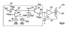
前記基本取得セルは、容量性センスノードと、前記容量性センスノードに連結されている光検出器及び焦電変換素子と、前記容量性センスノードを前記基本取得セルの導電性出力トラックに連結する読出し回路とを夫々有しており、
前記光検出器は、前記光源により照らされるユーザの皮膚から受ける光に応じて電荷を発生させ、前記焦電変換素子は、前記熱源により放射され前記皮膚によって変化する熱に応じて電荷を発生させ、
前記容量性センスノードは、発生した電荷に応じた静電容量を蓄積し、
前記導電性出力トラックは、紋様の光画像又は熱画像を取得すべく、前記容量性センスノードに蓄積された静電容量を前記読出し回路を介して読み出すことを特徴とするセンサ。 - 前記支持基板は、前記光源からの光を透過させるように構成されていることを特徴とする請求項1に記載のセンサ。
- 前記光検出器及び前記焦電変換素子は並列に接続されていることを特徴とする請求項1又は2に記載のセンサ。
- 前記センサの基本取得セルによる熱画像の取得及び光画像の取得を制御することが可能な回路を更に備えており、
該回路は、光画像取得段階全体に亘って前記光源をオンして前記熱源のオフを継続し、熱画像取得段階全体に亘って前記光源のオフを継続することが可能であることを特徴とする請求項1乃至3のいずれか一項に記載のセンサ。 - 前記センサの基本取得セルによる熱画像の取得及び光画像の取得を制御することが可能な回路を更に備えており、
該回路は、前記光源がオンである光画像取得段階の集積期間の一部で前記熱源をオンしてオフし、熱画像の取得を実行することが可能であることを特徴とする請求項1乃至3のいずれか一項に記載のセンサ。 - 各基本取得セルでは、前記光検出器及び前記焦電変換素子は前記容量性センスノードに直接連結されていることを特徴とする請求項1乃至5のいずれか一項に記載のセンサ。
- 各基本取得セルでは、前記光検出器及び前記焦電変換素子は前記基本取得セルの中間ノードに接続されており、該中間ノードは、選択トランジスタを介して前記容量性センスノードに連結されており、
各基本取得セルは、
前記容量性センスノードに接続された基準コンデンサと、
前記容量性センスノードに接続された電極と
を更に有しており、
該電極は、誘電体層で覆われて、紋様画像を容量的に取得するためにユーザの皮膚と共に静電容量を形成するように構成されていることを特徴とする請求項1乃至5のいずれか一項に記載のセンサ。 - 前記光検出器及び前記焦電変換素子は、オフ状態で前記光検出器を前記焦電変換素子から絶縁し得る同一の選択トランジスタに接続されていることを特徴とする請求項1又は2に記載のセンサ。
- 前記基本取得セルは行列のアレイに配置されており、
前記熱源は前記基本取得セルを一行毎に加熱すべく制御可能であることを特徴とする請求項1乃至8のいずれか一項に記載のセンサ。 - 前記基本取得セルは電圧読出しセルであり、
各電圧読出しセルは、前記容量性センスノードをリセット電位が与えられるノードに連結するリセットトランジスタを更に有しており、
前記電圧読出しセルの前記読出し回路は、フォロワソースとして組み立てられて、ゲートが前記容量性センスノードに接続されて、ソースが読出しトランジスタを介して前記電圧読出しセルの前記導電性出力トラックに連結されているトランジスタを有していることを特徴とする請求項1乃至9のいずれか一項に記載のセンサ。 - 前記基本取得セルは電荷読出しセルであり、
各電荷読出しセルの前記読出し回路は、前記容量性センスノードを前記電荷読出しセルの前記導電性出力トラックに連結する読出しトランジスタを有していることを特徴とする請求項1乃至9のいずれか一項に記載のセンサ。
Applications Claiming Priority (3)
| Application Number | Priority Date | Filing Date | Title |
|---|---|---|---|
| FR1459494A FR3026877B1 (fr) | 2014-10-03 | 2014-10-03 | Capteur d'empreintes digitales ou palmaires |
| FR1459494 | 2014-10-03 | ||
| PCT/FR2015/052616 WO2016051087A1 (fr) | 2014-10-03 | 2015-09-30 | Capteur d'empreintes digitales ou palmaires |
Publications (2)
| Publication Number | Publication Date |
|---|---|
| JP2017538101A JP2017538101A (ja) | 2017-12-21 |
| JP6741657B2 true JP6741657B2 (ja) | 2020-08-19 |
Family
ID=52465481
Family Applications (1)
| Application Number | Title | Priority Date | Filing Date |
|---|---|---|---|
| JP2017518055A Active JP6741657B2 (ja) | 2014-10-03 | 2015-09-30 | 指紋又は掌紋のセンサ |
Country Status (7)
| Country | Link |
|---|---|
| US (1) | US10176357B2 (ja) |
| EP (1) | EP3201832B1 (ja) |
| JP (1) | JP6741657B2 (ja) |
| KR (1) | KR20170104439A (ja) |
| CN (1) | CN107004125B (ja) |
| FR (1) | FR3026877B1 (ja) |
| WO (1) | WO2016051087A1 (ja) |
Families Citing this family (47)
| Publication number | Priority date | Publication date | Assignee | Title |
|---|---|---|---|---|
| CN104915657B (zh) * | 2015-06-29 | 2018-09-18 | 京东方科技集团股份有限公司 | 基于ltps技术的掌纹识别电路、掌纹识别方法以及显示屏 |
| FR3046277B1 (fr) * | 2015-12-23 | 2018-02-16 | Commissariat A L'energie Atomique Et Aux Energies Alternatives | Procede pour reconnaitre une fausse empreinte papillaire par eclairage structure |
| CN105631432B (zh) * | 2016-01-04 | 2020-12-08 | 京东方科技集团股份有限公司 | 指纹探测电路及驱动方法和显示装置 |
| US10656255B2 (en) | 2016-05-04 | 2020-05-19 | Invensense, Inc. | Piezoelectric micromachined ultrasonic transducer (PMUT) |
| US10315222B2 (en) | 2016-05-04 | 2019-06-11 | Invensense, Inc. | Two-dimensional array of CMOS control elements |
| US10670716B2 (en) | 2016-05-04 | 2020-06-02 | Invensense, Inc. | Operating a two-dimensional array of ultrasonic transducers |
| US10445547B2 (en) | 2016-05-04 | 2019-10-15 | Invensense, Inc. | Device mountable packaging of ultrasonic transducers |
| US10325915B2 (en) | 2016-05-04 | 2019-06-18 | Invensense, Inc. | Two-dimensional array of CMOS control elements |
| US11673165B2 (en) | 2016-05-10 | 2023-06-13 | Invensense, Inc. | Ultrasonic transducer operable in a surface acoustic wave (SAW) mode |
| US10632500B2 (en) | 2016-05-10 | 2020-04-28 | Invensense, Inc. | Ultrasonic transducer with a non-uniform membrane |
| US10562070B2 (en) | 2016-05-10 | 2020-02-18 | Invensense, Inc. | Receive operation of an ultrasonic sensor |
| US10600403B2 (en) | 2016-05-10 | 2020-03-24 | Invensense, Inc. | Transmit operation of an ultrasonic sensor |
| US10408797B2 (en) | 2016-05-10 | 2019-09-10 | Invensense, Inc. | Sensing device with a temperature sensor |
| US10706835B2 (en) | 2016-05-10 | 2020-07-07 | Invensense, Inc. | Transmit beamforming of a two-dimensional array of ultrasonic transducers |
| US10441975B2 (en) | 2016-05-10 | 2019-10-15 | Invensense, Inc. | Supplemental sensor modes and systems for ultrasonic transducers |
| US10452887B2 (en) | 2016-05-10 | 2019-10-22 | Invensense, Inc. | Operating a fingerprint sensor comprised of ultrasonic transducers |
| US10539539B2 (en) | 2016-05-10 | 2020-01-21 | Invensense, Inc. | Operation of an ultrasonic sensor |
| FR3054698B1 (fr) * | 2016-07-29 | 2018-09-28 | Commissariat A L'energie Atomique Et Aux Energies Alternatives | Capteur de motif thermique actif comprenant une matrice passive de pixels |
| US10162462B2 (en) * | 2017-05-01 | 2018-12-25 | Synaptics Incorporated | Integrating capacitive sensing with an optical sensor |
| US10891461B2 (en) | 2017-05-22 | 2021-01-12 | Invensense, Inc. | Live fingerprint detection utilizing an integrated ultrasound and infrared sensor |
| US10474862B2 (en) | 2017-06-01 | 2019-11-12 | Invensense, Inc. | Image generation in an electronic device using ultrasonic transducers |
| US10643052B2 (en) | 2017-06-28 | 2020-05-05 | Invensense, Inc. | Image generation in an electronic device using ultrasonic transducers |
| WO2019109010A1 (en) * | 2017-12-01 | 2019-06-06 | Invensense, Inc. | Darkfield tracking |
| US10997388B2 (en) | 2017-12-01 | 2021-05-04 | Invensense, Inc. | Darkfield contamination detection |
| US10984209B2 (en) | 2017-12-01 | 2021-04-20 | Invensense, Inc. | Darkfield modeling |
| FR3075954B1 (fr) * | 2017-12-22 | 2020-01-10 | Commissariat A L'energie Atomique Et Aux Energies Alternatives | Capteur pyroelectrique avec blindage electro-magnetique comprenant un materiau composite. |
| US11151355B2 (en) | 2018-01-24 | 2021-10-19 | Invensense, Inc. | Generation of an estimated fingerprint |
| TWI652625B (zh) | 2018-03-16 | 2019-03-01 | 友達光電股份有限公司 | 指紋感測裝置 |
| US10755067B2 (en) | 2018-03-22 | 2020-08-25 | Invensense, Inc. | Operating a fingerprint sensor comprised of ultrasonic transducers |
| US10937835B2 (en) * | 2018-11-21 | 2021-03-02 | BAE Systems Imaging Solutions Inc. | Low-noise integrated post-processed photodiode |
| US10936843B2 (en) | 2018-12-28 | 2021-03-02 | Invensense, Inc. | Segmented image acquisition |
| CN111404533B (zh) * | 2019-01-02 | 2022-06-03 | 京东方科技集团股份有限公司 | 检测电路、纹路识别装置及驱动方法 |
| CN110135348B (zh) * | 2019-05-15 | 2021-02-09 | 京东方科技集团股份有限公司 | 指纹检测电路及其驱动方法、阵列基板、显示装置 |
| CN110287808B (zh) * | 2019-06-03 | 2022-01-14 | 京东方科技集团股份有限公司 | 阵列基板及其制造方法,以及显示面板和显示装置 |
| US11188735B2 (en) | 2019-06-24 | 2021-11-30 | Invensense, Inc. | Fake finger detection using ridge features |
| WO2020264046A1 (en) | 2019-06-25 | 2020-12-30 | Invensense, Inc. | Fake finger detection based on transient features |
| US11216632B2 (en) | 2019-07-17 | 2022-01-04 | Invensense, Inc. | Ultrasonic fingerprint sensor with a contact layer of non-uniform thickness |
| US11176345B2 (en) | 2019-07-17 | 2021-11-16 | Invensense, Inc. | Ultrasonic fingerprint sensor with a contact layer of non-uniform thickness |
| US11232549B2 (en) | 2019-08-23 | 2022-01-25 | Invensense, Inc. | Adapting a quality threshold for a fingerprint image |
| US20220004729A1 (en) * | 2019-08-29 | 2022-01-06 | Boe Technology Group Co., Ltd. | Fingerprint identification circuit and driving method thereof, fingerprint identification module, and display device |
| US11392789B2 (en) | 2019-10-21 | 2022-07-19 | Invensense, Inc. | Fingerprint authentication using a synthetic enrollment image |
| EP4100176A1 (en) | 2020-03-09 | 2022-12-14 | InvenSense, Inc. | Ultrasonic fingerprint sensor with a contact layer of non-uniform thickness |
| US11243300B2 (en) | 2020-03-10 | 2022-02-08 | Invensense, Inc. | Operating a fingerprint sensor comprised of ultrasonic transducers and a presence sensor |
| US11328165B2 (en) | 2020-04-24 | 2022-05-10 | Invensense, Inc. | Pressure-based activation of fingerprint spoof detection |
| CN112699853B (zh) * | 2021-01-28 | 2024-02-02 | 合肥维信诺科技有限公司 | 指纹识别电路及其驱动方法、指纹识别设备 |
| US11380126B1 (en) * | 2021-02-04 | 2022-07-05 | Himax Technologies Limited | Display device with embedded biometric detection function in active region |
| US11886666B1 (en) * | 2022-08-08 | 2024-01-30 | Himax Technologies Limited | Fingerprint detection system and a detection circuit adaptable thereto |
Family Cites Families (13)
| Publication number | Priority date | Publication date | Assignee | Title |
|---|---|---|---|---|
| GB1105828A (en) | 1964-12-14 | 1968-03-13 | Allied Chem | Fumaric acid beverage mixes |
| JPH1079499A (ja) * | 1996-09-05 | 1998-03-24 | Nikon Corp | 受光素子およびこれを用いたイメージセンサ |
| GB9804539D0 (en) * | 1998-03-05 | 1998-04-29 | Philips Electronics Nv | Fingerprint sensing devices and systems incorporating such |
| FR2781927B1 (fr) * | 1998-07-28 | 2001-10-05 | Commissariat Energie Atomique | Dispositif de detection de rayonnements multispectraux infrarouge/visible |
| JP3559754B2 (ja) * | 2000-07-25 | 2004-09-02 | Necエレクトロニクス株式会社 | 指紋認証装置 |
| US7088443B2 (en) * | 2002-02-11 | 2006-08-08 | Kla-Tencor Technologies Corporation | System for detecting anomalies and/or features of a surface |
| JP2006343229A (ja) * | 2005-06-09 | 2006-12-21 | Mitsubishi Electric Corp | イメージセンサ |
| RU2534018C2 (ru) * | 2010-06-01 | 2014-11-27 | Боли Медиа Коммуникейшнз (Шэньчжэнь) Ко., Лтд | Мультиспектральные фоточувствительные устройства и способы для их дискретизации |
| EP2710582A4 (en) * | 2011-05-17 | 2014-12-31 | Cross Match Technologies Inc | DIGITAL FOOTPRINT SENSORS |
| CN103136507A (zh) * | 2011-11-26 | 2013-06-05 | 陈亘朝 | 指纹形混合识别装置 |
| FR2999338B1 (fr) * | 2012-12-10 | 2017-12-08 | Soc Fr De Detecteurs Infrarouges - Sofradir | Imageur monolithique multispectral visible et infrarouge |
| US9465429B2 (en) * | 2013-06-03 | 2016-10-11 | Qualcomm Incorporated | In-cell multifunctional pixel and display |
| KR101376228B1 (ko) * | 2013-07-17 | 2014-04-01 | 실리콘 디스플레이 (주) | 광학식 및 정전용량방식으로 지문인식이 가능한 지문인식센서 |
-
2014
- 2014-10-03 FR FR1459494A patent/FR3026877B1/fr active Active
-
2015
- 2015-09-30 KR KR1020177011066A patent/KR20170104439A/ko not_active Application Discontinuation
- 2015-09-30 EP EP15788117.8A patent/EP3201832B1/fr active Active
- 2015-09-30 WO PCT/FR2015/052616 patent/WO2016051087A1/fr active Application Filing
- 2015-09-30 US US15/516,402 patent/US10176357B2/en active Active
- 2015-09-30 CN CN201580065747.8A patent/CN107004125B/zh active Active
- 2015-09-30 JP JP2017518055A patent/JP6741657B2/ja active Active
Also Published As
| Publication number | Publication date |
|---|---|
| US10176357B2 (en) | 2019-01-08 |
| WO2016051087A1 (fr) | 2016-04-07 |
| CN107004125A (zh) | 2017-08-01 |
| JP2017538101A (ja) | 2017-12-21 |
| EP3201832A1 (fr) | 2017-08-09 |
| US20170293791A1 (en) | 2017-10-12 |
| FR3026877A1 (fr) | 2016-04-08 |
| EP3201832B1 (fr) | 2018-10-10 |
| CN107004125B (zh) | 2021-06-15 |
| FR3026877B1 (fr) | 2018-01-05 |
| KR20170104439A (ko) | 2017-09-15 |
Similar Documents
| Publication | Publication Date | Title |
|---|---|---|
| JP6741657B2 (ja) | 指紋又は掌紋のセンサ | |
| US10380400B2 (en) | Fingerprint or palmprint sensor | |
| US11303857B2 (en) | Imaging device including pixel array and addition circuit | |
| TWI345912B (en) | Physical quantity distribution detecting apparatus and imaging apparatus | |
| CA2204553C (en) | High sensitivity image sensor arrays | |
| KR101672344B1 (ko) | 광센싱 회로, 상기 광센싱 회로의 구동 방법, 및 상기 광센싱 회로를 채용한 광센싱 장치 | |
| JP7209340B2 (ja) | 撮像装置 | |
| TW201143417A (en) | Solid-state image pickup apparatus, signal processing method for a solid-state image pickup apparatus, and electronic apparatus | |
| US20170054922A1 (en) | Infrared imager readout electronics | |
| US20170302872A1 (en) | Solid-state imaging device, signal processing method, and electronic device | |
| US10186512B2 (en) | Solid-state image sensor, image capturing device, and electronic device | |
| JPWO2014049901A1 (ja) | 固体撮像装置 | |
| US10586088B2 (en) | Pyroelectric sensor for the detection of skin prints | |
| WO2017122542A1 (ja) | 撮像素子、撮像素子の駆動方法、並びに、電子機器 | |
| JP2021036662A (ja) | イメージセンサ及びイメージセンサを備えるイメージングシステム | |
| CN110557585A (zh) | 图像传感器、操作图像传感器的方法及系统 | |
| JP2011149932A (ja) | 赤外線検出回路、センサーデバイス及び電子機器 | |
| US10044965B2 (en) | Method for image capture of TFT flat-panel image sensor | |
| WO2021112742A1 (en) | Tft-based fingerprint sensing system with corrected read-out | |
| CN109863603B (zh) | 具有电子收集电极和空穴收集电极的图像传感器 | |
| US11134213B2 (en) | Pixel array and image sensor | |
| US20190058010A1 (en) | Methods and systems for manufacturing image sensors | |
| JP5061687B2 (ja) | フォトセンサ、フォトセンサアレイ、フォトセンサシステム及びフォトセンサシステムの駆動制御方法 | |
| JP2021027985A (ja) | 熱パターンを採取するためのセンサおよび二重積分方法 | |
| JP2003153083A (ja) | フォトセンサシステム及びフォトセンサシステムにおけるフォトセンサの駆動制御方法 |
Legal Events
| Date | Code | Title | Description |
|---|---|---|---|
| A621 | Written request for application examination |
Free format text: JAPANESE INTERMEDIATE CODE: A621 Effective date: 20180905 |
|
| A977 | Report on retrieval |
Free format text: JAPANESE INTERMEDIATE CODE: A971007 Effective date: 20190314 |
|
| A131 | Notification of reasons for refusal |
Free format text: JAPANESE INTERMEDIATE CODE: A131 Effective date: 20190326 |
|
| A521 | Request for written amendment filed |
Free format text: JAPANESE INTERMEDIATE CODE: A523 Effective date: 20190624 |
|
| A131 | Notification of reasons for refusal |
Free format text: JAPANESE INTERMEDIATE CODE: A131 Effective date: 20191001 |
|
| A521 | Request for written amendment filed |
Free format text: JAPANESE INTERMEDIATE CODE: A523 Effective date: 20191227 |
|
| TRDD | Decision of grant or rejection written | ||
| A01 | Written decision to grant a patent or to grant a registration (utility model) |
Free format text: JAPANESE INTERMEDIATE CODE: A01 Effective date: 20200714 |
|
| A61 | First payment of annual fees (during grant procedure) |
Free format text: JAPANESE INTERMEDIATE CODE: A61 Effective date: 20200727 |
|
| R150 | Certificate of patent or registration of utility model |
Ref document number: 6741657 Country of ref document: JP Free format text: JAPANESE INTERMEDIATE CODE: R150 |