JP6738193B2 - Heat transfer structure, insulating laminated material, insulating circuit board and power module base - Google Patents
Heat transfer structure, insulating laminated material, insulating circuit board and power module base Download PDFInfo
- Publication number
- JP6738193B2 JP6738193B2 JP2016093934A JP2016093934A JP6738193B2 JP 6738193 B2 JP6738193 B2 JP 6738193B2 JP 2016093934 A JP2016093934 A JP 2016093934A JP 2016093934 A JP2016093934 A JP 2016093934A JP 6738193 B2 JP6738193 B2 JP 6738193B2
- Authority
- JP
- Japan
- Prior art keywords
- heat
- heat transfer
- power module
- wall
- casing
- Prior art date
- Legal status (The legal status is an assumption and is not a legal conclusion. Google has not performed a legal analysis and makes no representation as to the accuracy of the status listed.)
- Active
Links
- 239000002648 laminated material Substances 0.000 title claims description 13
- 239000000463 material Substances 0.000 claims description 59
- 239000004065 semiconductor Substances 0.000 claims description 45
- OKTJSMMVPCPJKN-UHFFFAOYSA-N Carbon Chemical compound [C] OKTJSMMVPCPJKN-UHFFFAOYSA-N 0.000 claims description 26
- 229910002804 graphite Inorganic materials 0.000 claims description 24
- 239000010439 graphite Substances 0.000 claims description 24
- 238000010438 heat treatment Methods 0.000 claims description 21
- 230000002093 peripheral effect Effects 0.000 claims description 21
- 238000004891 communication Methods 0.000 claims description 14
- 229910052751 metal Inorganic materials 0.000 claims description 6
- 239000002184 metal Substances 0.000 claims description 6
- 238000009413 insulation Methods 0.000 claims description 2
- 229910052782 aluminium Inorganic materials 0.000 description 15
- XAGFODPZIPBFFR-UHFFFAOYSA-N aluminium Chemical compound [Al] XAGFODPZIPBFFR-UHFFFAOYSA-N 0.000 description 15
- 239000000110 cooling liquid Substances 0.000 description 12
- 230000005855 radiation Effects 0.000 description 10
- 238000005219 brazing Methods 0.000 description 7
- 230000006866 deterioration Effects 0.000 description 5
- 230000017525 heat dissipation Effects 0.000 description 5
- 239000002131 composite material Substances 0.000 description 4
- 239000000470 constituent Substances 0.000 description 4
- 239000000919 ceramic Substances 0.000 description 3
- 238000001816 cooling Methods 0.000 description 3
- 230000000149 penetrating effect Effects 0.000 description 3
- 238000004519 manufacturing process Methods 0.000 description 2
- 229910018072 Al 2 O 3 Inorganic materials 0.000 description 1
- 229910000838 Al alloy Inorganic materials 0.000 description 1
- 238000006243 chemical reaction Methods 0.000 description 1
- 239000012809 cooling fluid Substances 0.000 description 1
- 238000009792 diffusion process Methods 0.000 description 1
- 238000005304 joining Methods 0.000 description 1
- 238000000034 method Methods 0.000 description 1
- 238000012986 modification Methods 0.000 description 1
- 230000004048 modification Effects 0.000 description 1
Images


Description
この発明は、伝熱構造体、絶縁積層材、絶縁回路基板およびパワーモジュール用ベースに関し、さらに詳しくは、たとえば電力変換装置などのパワーモジュールを構成し、かつIGBTなどのパワーモジュール用半導体素子が実装される絶縁回路基板に用いられる絶縁積層材、絶縁積層材からなる絶縁回路基板、および絶縁回路基板に実装されたパワーモジュール用半導体素子を冷却するのに用いられるパワーモジュール用ベースに関する。 The present invention relates to a heat transfer structure, an insulating laminated material, an insulating circuit board, and a power module base. More specifically, for example, a power module such as a power converter is configured and a power module semiconductor element such as an IGBT is mounted. The present invention relates to an insulating laminated material used for an insulated circuit board, an insulating circuit board made of the insulating laminated material, and a power module base used for cooling a power module semiconductor element mounted on the insulating circuit board.
この明細書および特許請求の範囲において、図1、図3および図4の上下を上下というものとする。 In this specification and claims, the top and bottom of FIGS. 1, 3 and 4 are referred to as the top and bottom.
たとえば、電気自動車、ハイブリッド自動車、電車などの車両に搭載される電力変換装置として用いられるパワーモジュールにおいては、IGBTなどの半導体素子から発せられる熱を効率良く放熱して、パワーモジュール用半導体素子の温度を所定温度以下に保つ必要がある。 For example, in a power module used as a power conversion device mounted on a vehicle such as an electric vehicle, a hybrid vehicle, and an electric train, heat generated from a semiconductor element such as an IGBT is efficiently dissipated, and the temperature of the semiconductor element for a power module is reduced. Must be kept below a predetermined temperature.
従来、電力変換装置などのパワーモジュールとして、アルミニウム製冷却器および冷却器にろう付された絶縁回路基板からなるパワーモジュール用ベースと、パワーモジュール用ベースの絶縁回路基板に実装されたパワーモジュール用半導体素子とよりなり、パワーモジュール用ベースが、セラミック製絶縁板、絶縁板の一面にろう付された板状のアルミニウム製第1熱伝導部材(回路板)および絶縁板の他面にろう付された板状のアルミニウム製第2熱伝導部材(伝熱板)よりなる絶縁回路基板(絶縁積層材)と、絶縁回路基板の第2熱伝導板における絶縁板にろう付された面と反対側の面にろう付されたアルミニウム製冷却器とからなり、絶縁回路基板の回路板における絶縁板にろう付された面とは反対側の面が、半導体素子搭載部を有する配線面となされ、当該配線面の半導体素子搭載部にパワーモジュール用半導体素子が実装されているパワーモジュールが知られている(特許文献1参照)。 Conventionally, as a power module for a power converter, a power module base including an aluminum cooler and an insulating circuit board brazed to the cooler, and a power module semiconductor mounted on the insulating circuit board of the power module base. A power module base made up of elements, a ceramic insulating plate, a plate-shaped aluminum first heat conducting member (circuit board) brazed to one surface of the insulating plate, and another surface of the insulating plate An insulating circuit board (insulating laminated material) made of a plate-shaped aluminum second heat conducting member (heat transfer plate), and a surface of the second heat conducting plate of the insulating circuit board opposite to the surface brazed to the insulating plate And a surface of the circuit board of the insulating circuit board opposite to the surface brazed to the insulating plate is a wiring surface having a semiconductor element mounting portion. There is known a power module in which a semiconductor element for a power module is mounted on the semiconductor element mounting part (see Patent Document 1).
特許文献1記載のパワーモジュールにおいては、パワーモジュール用半導体素子から発せられた熱は、回路板、絶縁板および伝熱板を経て冷却器に伝えられ、放熱されるようになっている。
In the power module described in
ところで、最近では、パワーモジュール用半導体素子としては高耐熱性を有するものが開発されて小型化が図られているが、上述した車両の高効率化に伴って、出力電流は増大する傾向にあり、熱源の集中が進んでいる。 By the way, recently, as a semiconductor element for a power module, one having high heat resistance has been developed and miniaturized, but the output current tends to increase with the increase in efficiency of the vehicle described above. , Heat sources are becoming more concentrated.
しかしながら、熱源が集中した場合、特許文献1記載のパワーモジュールにおいては、パワーモジュール用半導体素子から発せられた熱が冷却器まで伝わる間に、絶縁板、第1熱伝導部材および第2熱伝導部材の上下両面の面方向に拡散しにくくなり、有効に利用しうる冷却器の冷却範囲が小さくなって放熱効率が低下するおそれがある。
However, when the heat source is concentrated, in the power module described in
そこで、特許文献1記載のパワーモジュールに用いられている絶縁回路基板の第1熱伝導部材および第2熱伝導部材として、グラファイトシートと、グラファイトシートの両主面および側面を覆うアルミニウム製シートとからなるグラファイト複合材(特許文献2参照)を用いることが考えられる。特許文献2記載のグラファイト複合材を上記第1熱伝導部材および第2熱伝導部材に用いたパワーモジュールによれば、パワーモジュール用半導体素子から発せられた熱は、第1熱伝導部材および第2熱伝導部材においてグラファイトシート内を主面方向に広がりながら冷却器に伝わる。
Therefore, a graphite sheet and an aluminum sheet covering both main surfaces and side surfaces of the graphite sheet are used as the first heat conducting member and the second heat conducting member of the insulated circuit board used in the power module described in
しかしながら、特許文献2記載のグラファイト複合材においては、グラファイトシートの両主面と、両主面を覆う金属シートとの間に隙間が発生しやすく、グラファイト複合材の厚み方向の伝熱性が不足し、パワーモジュール用半導体素子から発せられる熱の放熱性能が低下するおそれがある。
However, in the graphite composite material described in
この発明の目的は、上記問題を解決し、パワーモジュール用ベースの絶縁回路基板の第1熱伝導部材および第2熱伝導部材に用いた場合にパワーモジュール用半導体素子から発せられる熱の放熱性能の低下を抑制しうる伝熱構造体と、伝熱構造体を用いた絶縁積層材、絶縁回路基板およびパワーモジュール用ベースを提供することにある。 An object of the present invention is to solve the above problems and to improve the heat radiation performance of heat generated from a semiconductor element for a power module when used for the first heat conduction member and the second heat conduction member of the insulated circuit board of the power module base. It is intended to provide a heat transfer structure capable of suppressing a decrease, an insulating laminated material using the heat transfer structure, an insulating circuit board, and a power module base.
本発明は、上記目的を達成するために以下の態様からなる。 The present invention has the following aspects in order to achieve the above object.
1)上壁、下壁および囲繞壁を有する中空状の金属製ケーシングと、ケーシング内に入れられたグラファイトからなる伝熱材料とを備えており、ケーシングの上壁と下壁との間に、長手方向を上下方向に向けるとともに伝熱材料を貫通した複数の金属製連結部材が配置され、ケーシングの上壁および下壁と、連結部材の上端および下端とがそれぞれ固定されている伝熱構造体。 1) a hollow metal casing having an upper wall, a lower wall and a surrounding wall, and a heat transfer material made of graphite contained in the casing, and between the upper and lower walls of the casing, A heat transfer structure in which a plurality of metal connecting members having longitudinal directions oriented vertically and penetrating a heat transfer material are arranged, and an upper wall and a lower wall of a casing and an upper end and a lower end of the connecting member are fixed, respectively. ..
2)伝熱材料が、厚み方向を上下方向に向けて配置された1枚のグラファイトシートからなり、当該グラファイトシートからなる伝熱材料に上下方向を向いた貫通穴が複数形成され、当該貫通穴に連通部材が通され、貫通穴の内周面に連通部材の外周面が接している上記1)記載の伝熱構造体。 2) The heat transfer material is composed of a single graphite sheet arranged with the thickness direction oriented vertically, and the heat transfer material made of the graphite sheet is provided with a plurality of through holes oriented in the vertical direction. The heat transfer structure according to 1) above, wherein the communication member is passed through, and the outer peripheral surface of the communication member is in contact with the inner peripheral surface of the through hole.
3)伝熱材料が、厚み方向を上下方向に向けて配置された複数枚のグラファイトシートが上下方向に重ね合わされた積層体からなり、当該積層体からなる伝熱材料に上下方向を向いた貫通穴が複数形成され、当該貫通穴に連通部材が通され、貫通穴の内周面に連通部材の外周面が接している上記1)記載の伝熱構造体。 3) The heat transfer material is composed of a laminated body in which a plurality of graphite sheets arranged with the thickness direction oriented in the vertical direction are stacked in the vertical direction, and the heat transfer material composed of the laminated body penetrates in the vertical direction. The heat transfer structure according to 1), wherein a plurality of holes are formed, a communication member is passed through the through hole, and an outer peripheral surface of the communication member is in contact with an inner peripheral surface of the through hole.
4)グラファイトシートの厚みが0.125mm以上である上記3)記載の伝熱構造体。 4) The heat transfer structure according to 3) above, wherein the graphite sheet has a thickness of 0.125 mm or more.
5)伝熱材料が、グラファイト粉末の結合体からなり、当該結合体からなる伝熱材料に、上下方向を向いた貫通穴が複数形成され、当該貫通穴に連通部材が通され、貫通穴の内周面に連通部材の外周面が接している上記1)記載の伝熱構造体。 5) The heat transfer material is composed of a combination of graphite powder, a plurality of through holes oriented in the vertical direction are formed in the heat transfer material formed of the combination, and a communication member is passed through the through hole, The heat transfer structure according to 1), wherein the outer peripheral surface of the communication member is in contact with the inner peripheral surface.
6)伝熱材料が、1枚のグラファイトシートによりコルゲート状に形成され、かつ互いに平行な複数の垂直壁部および隣り合う垂直壁部を上下交互に連結する連結部からなり、当該コルゲート状伝熱材料に上下方向を向いた貫通穴が複数形成され、当該貫通穴に連通部材が通され、貫通穴の内周面に連通部材の外周面が接している上記1)記載の伝熱構造体。 6) The heat transfer material is formed of a single graphite sheet in a corrugated shape, and includes a plurality of vertical wall portions parallel to each other and a connecting portion that vertically connects the adjacent vertical wall portions, and the corrugated heat transfer material is formed. The heat transfer structure according to the above 1), wherein a plurality of through-holes oriented in the vertical direction are formed in the material, the communication member is passed through the through-hole, and the outer peripheral surface of the communication member is in contact with the inner peripheral surface of the through-hole.
7)絶縁板と、絶縁板の片面に接合されかつ絶縁板とは反対側の面が発熱体取付面となっている板状の第1熱伝導部材と、絶縁板の他面に接合された板状の第2熱伝導部材とよりなり、第1熱伝導部材の発熱体取付面に取り付けられる発熱体から発せられる熱が、第1熱伝導部材および絶縁板を経て第2熱伝導部材に伝わるようになされている絶縁積層材であって、
第1熱伝導部材および第2熱伝導部材が、上記1)〜6)のうちのいずれかに記載の伝熱構造体からなる絶縁積層材。
7) An insulating plate, a plate-shaped first heat conducting member joined to one surface of the insulating plate and having a surface opposite to the insulating plate as a heating element mounting surface, and joined to the other surface of the insulating plate The heat generated from the heating element, which is made of a plate-shaped second heat conduction member and is attached to the heating element attachment surface of the first heat conduction member, is transmitted to the second heat conduction member via the first heat conduction member and the insulating plate. It is an insulating laminated material that is made like
An insulating laminated material in which the first heat conducting member and the second heat conducting member are the heat transfer structures according to any one of 1) to 6) above.
8)上記7)記載の絶縁積層材の第1熱伝導部材の発熱体取付面が、発熱体となる半導体素子を搭載する半導体素子搭載部を有する配線面となされている絶縁回路基板。 8) An insulated circuit board in which the heating element mounting surface of the first heat conductive member of the insulating laminated material described in 7) above is a wiring surface having a semiconductor element mounting portion on which a semiconductor element serving as a heating element is mounted.
9)上記8)記載の絶縁回路基板の第2熱伝導部材における絶縁板と接合された面とは反対側の面が、冷却器に接合されているパワーモジュール用ベース。 9) A power module base in which a surface of the second heat conductive member of the above-mentioned insulated circuit board opposite to a surface thereof joined to the insulating plate is joined to the cooler.
上記1)〜6)の伝熱構造体によれば、上壁、下壁および囲繞壁を有する中空状の金属製ケーシングと、ケーシング内に入れられたグラファイトからなる伝熱材料とを備えており、ケーシングの上壁と下壁との間に、長手方向を上下方向に向けるとともに伝熱材料を貫通した複数の金属製連結部材が配置され、ケーシングの上壁および下壁と、連結部材の上端および下端とがそれぞれ固定されているので、連結部材の働きによって、ケーシングの上壁および下壁と、伝熱材料の上面および下面との間に隙間が発生することが抑制される。したがって、当該伝熱構造体をパワーモジュール用ベースの絶縁回路基板の第1熱伝導部材および第2熱伝導部材に用いた場合に、パワーモジュール用半導体素子から発せられる熱の放熱性能の低下を抑制することが可能になる。 According to the heat transfer structure of the above 1) ~ 6), it is provided with a hollow metal casing having an upper wall, a lower wall and a surrounding wall, and a heat transfer material made of graphite placed in the casing. , A plurality of metallic connecting members having longitudinal directions oriented vertically and penetrating a heat transfer material are arranged between the upper wall and the lower wall of the casing, and the upper and lower walls of the casing and the upper end of the connecting member. Since the lower end and the lower end are fixed, the action of the connecting member suppresses the generation of a gap between the upper wall and the lower wall of the casing and the upper surface and the lower surface of the heat transfer material. Therefore, when the heat transfer structure is used for the first heat conduction member and the second heat conduction member of the insulated circuit board of the power module base, reduction in heat radiation performance of heat generated from the power module semiconductor element is suppressed. It becomes possible to do.
また、ケーシングの上壁や下壁に、パワーモジュール用半導体素子や絶縁板などの上壁および下壁を構成する材料と線膨張率の異なる材料からなるものをろう付する際に熱歪みが生じたとしても、ケーシングの上壁および下壁と、伝熱材料の上面および下面との間に隙間が発生することが抑制される。 In addition, thermal distortion occurs when brazing the upper wall and the lower wall of the casing with a material having a different linear expansion coefficient from the material forming the upper wall and the lower wall such as the semiconductor element for a power module and the insulating plate. Even if it does, a gap is suppressed from being generated between the upper wall and the lower wall of the casing and the upper surface and the lower surface of the heat transfer material.
上記2)および3)の伝熱構造体によれば、ケーシングの上壁および下壁のうちいずれか一方の壁の外面に発熱体を取り付けた場合、発熱体から発せられた熱は、ケーシングの前記一方の壁を経て伝熱材料に伝わり、伝熱材料の上下両面の面方向に広がって連結部材に伝わるとともに、連結部材を通ってケーシングの他方の壁に伝わる。また、発熱体から発せられた熱は、ケーシングの前記一方の壁を経て連結部材に伝わるとともに、連結部材を通ってケーシングの他方の壁に伝わる。したがって、ケーシングの上壁と下壁との間の伝熱性が向上し、当該伝熱構造体をパワーモジュール用ベースの絶縁回路基板の第1熱伝導部材および第2熱伝導部材に用いた場合に、パワーモジュール用半導体素子から発せられる熱の放熱性能の低下を抑制することが可能になる。しかも、小型化されたパワーモジュール用半導体素子が用いられた際のように熱源が集中した場合であっても、熱は冷却器に伝わるまでの間に伝熱材料の面方向に拡散するので、有効に利用しうる冷却器の冷却範囲が大きくなって放熱効率が向上する。さらに、伝熱構造体を製造する際の伝熱材料の取り扱いが容易になる。 According to the heat transfer structure of the above 2) and 3), when the heating element is attached to the outer surface of either one of the upper wall and the lower wall of the casing, the heat generated from the heating element is The heat is transferred to the heat transfer material through the one wall, spreads in the plane directions of the upper and lower surfaces of the heat transfer material, transferred to the connecting member, and also transferred to the other wall of the casing through the connecting member. Further, the heat generated from the heating element is transmitted to the connecting member via the one wall of the casing and is transmitted to the other wall of the casing through the connecting member. Therefore, the heat transfer between the upper wall and the lower wall of the casing is improved, and when the heat transfer structure is used for the first heat conductive member and the second heat conductive member of the insulated circuit board of the power module base, Thus, it becomes possible to suppress the deterioration of the heat radiation performance of the heat generated from the power module semiconductor element. Moreover, even when the heat source is concentrated as in the case where a miniaturized power module semiconductor element is used, heat diffuses in the surface direction of the heat transfer material before it reaches the cooler. The cooling range of the cooler that can be effectively used is increased, and the heat radiation efficiency is improved. Further, the heat transfer material can be easily handled when manufacturing the heat transfer structure.
上記3)の伝熱構造体によれば、伝熱材料の厚みを任意に変更して、伝熱材料の上下両面の面方向への熱伝導性を最適化することができる。 According to the heat transfer structure of 3) above, the thickness of the heat transfer material can be arbitrarily changed to optimize the heat conductivity in the surface directions of the upper and lower surfaces of the heat transfer material.
上記4)の伝熱構造体によれば、伝熱材料の上下両面の面方向への熱伝導性が優れたものになる。 According to the heat transfer structure of 4) above, the heat transfer material has excellent heat conductivity in the surface directions of the upper and lower surfaces.
上記5)の伝熱構造体によれば、伝熱材料を安価にすることができる。 According to the heat transfer structure of 5) above, the heat transfer material can be inexpensive.
上記6)の伝熱構造体によれば、ケーシングの上壁および下壁のうちいずれか一方の壁の外面に発熱体を取り付けた場合、発熱体から発せられた熱は、ケーシングの前記一方の壁を経て伝熱材料に伝わり、伝熱材料の垂直壁部を高さ方向に通ってケーシングの他方の壁に伝わる。また、発熱体から発せられた熱は、ケーシングの前記一方の壁を経て伝熱材料に伝わり、伝熱材料の垂直壁部の長手方向に通って連結部材に伝わるとともに、連結部材を通ってケーシングの他方の壁に伝わる。さらに、発熱体から発せられた熱は、ケーシングの前記一方の壁を経て連結部材に伝わるとともに、連結部材を通ってケーシングの他方の壁に伝わる。したがって、ケーシングの上壁と下壁との間の伝熱性が向上し、当該伝熱構造体をパワーモジュール用ベースの絶縁回路基板の回路板および伝熱板に用いた場合に、パワーモジュール用半導体素子から発せられる熱の放熱性能の低下を抑制することが可能になる。 According to the heat transfer structure of 6) above, when the heating element is attached to the outer surface of either one of the upper wall and the lower wall of the casing, the heat generated from the heating element is The heat is transferred to the heat transfer material through the wall, passes through the vertical wall portion of the heat transfer material in the height direction, and is transferred to the other wall of the casing. Further, the heat generated from the heating element is transmitted to the heat transfer material through the one wall of the casing, is transmitted to the connecting member along the longitudinal direction of the vertical wall portion of the heat transfer material, and is also transmitted through the connecting member to the casing. Is transmitted to the other wall of. Further, the heat generated from the heating element is transmitted to the connecting member via the one wall of the casing and is transmitted to the other wall of the casing through the connecting member. Therefore, the heat transfer property between the upper wall and the lower wall of the casing is improved, and when the heat transfer structure is used for the circuit board and the heat transfer board of the insulating circuit board of the power module base, the semiconductor for power module is used. It is possible to suppress deterioration of heat dissipation performance of heat generated from the element.
上記7)の絶縁積層材からなる絶縁回路基板をパワーモジュール用ベースに用いたパワーモジュールによれば、パワーモジュール用半導体素子から発せられる熱の放熱性能の低下を抑制することが可能になる。 According to the power module in which the insulating circuit board made of the insulating laminated material described in 7) above is used for the power module base, it is possible to suppress deterioration of the heat radiation performance of the heat generated from the power module semiconductor element.
上記8)の絶縁回路基板をパワーモジュール用ベースに用いたパワーモジュールによれば、パワーモジュール用半導体素子から発せられる熱の放熱性能の低下を抑制することが可能になる。 According to the power module using the insulated circuit board of the above 8) as the power module base, it is possible to suppress deterioration of the heat radiation performance of the heat generated from the power module semiconductor element.
上記9)のパワーモジュール用ベースを用いたパワーモジュールによれば、パワーモジュール用半導体素子から発せられる熱の放熱性能の低下を抑制することが可能になる。 According to the power module using the power module base of the above 9), it is possible to suppress deterioration in heat dissipation performance of heat generated from the power module semiconductor element.
以下、この発明の実施形態を、図面を参照して説明する。 Embodiments of the present invention will be described below with reference to the drawings.
以下の説明において、図1の左右を左右というものとする。 In the following description, the left and right of FIG. 1 will be referred to as the left and right.
また、以下の説明において、「アルミニウム」という用語には、純アルミニウムの他にアルミニウム合金を含むものとする。 Further, in the following description, the term “aluminum” includes an aluminum alloy in addition to pure aluminum.
なお、全図面を通じて同一部分および同一物には同一符号を付して重複する説明を省略する。 Throughout the drawings, the same parts and the same parts will be denoted by the same reference symbols, without redundant description.
図1および図2はこの発明による伝熱構造体を示し、図3は図1および図2の伝熱構造体を有する絶縁回路基板を使用したパワーモジュール用ベースにパワーモジュール用半導体素子が実装されることにより構成されたパワーモジュールを示す。 1 and 2 show a heat transfer structure according to the present invention, and FIG. 3 shows a power module semiconductor element mounted on a power module base using an insulating circuit board having the heat transfer structure of FIGS. The power module comprised by this is shown.
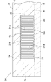
図1および図2において、伝熱構造体(1)は、上壁(2a)、下壁(2b)および囲繞壁(2c)を有する中空状のアルミニウム製ケーシング(2)と、ケーシング(2)内に入れられたグラファイトからなる伝熱材料(3)とを備えている。 1 and 2, the heat transfer structure (1) comprises a hollow aluminum casing (2) having an upper wall (2a), a lower wall (2b) and a surrounding wall (2c), and a casing (2). And a heat transfer material (3) made of graphite contained therein.
ケーシング(2)は、下方に開口した凹部(4a)を有し、かつ上壁(2a)および囲繞壁(2c)を構成するアルミニウム製上構成部材(4)と、平板状のアルミニウム製下構成部材(5)とよりなり、下構成部材(5)の上面周縁部が上構成部材(4)の囲繞壁(2c)となる部分の下端面にろう材により金属的に接合されている。以下、ろう材による接合をろう付と称するものとする。 The casing (2) has an aluminum upper component (4) having a recess (4a) opening downward and constituting the upper wall (2a) and the surrounding wall (2c), and a flat aluminum lower component. The upper component of the lower component (5) is joined to the lower end surface of the upper component (4) to be the surrounding wall (2c) by a brazing material. Hereinafter, joining with a brazing material will be referred to as brazing.
ケーシング(2)の上壁(2a)と下壁(2b)との間には、長手方向を上下方向に向けるとともに伝熱材料(3)を貫通した横断面円形のアルミニウム製連結部材(6)が千鳥配置状に複数設けられ、ケーシング(2)の上壁(2a)および下壁(2b)と、連結部材(6)の上端および下端とがそれぞれ固定されている。この実施形態においては、ケーシング(2)の上構成部材(4)における上壁(2a)となる部分の下面に連結部材(6)が一体に形成されており、連結部材(6)の下端面が下構成部材(5)の上面にろう付、拡散接合などによって金属的に接合されている。しかしながら、ケーシング(2)の下構成部材(5)の上面に連結部材(6)が一体に形成されており、連結部材(6)の上端面が上構成部材(4)の上壁(2a)となる部分の下面に金属的に接合されていてもよく、あるいは連結部材(6)はケーシング(2)の上下両構成部材(4)(5)とは別個に形成され、連結部材(6)の上端面が上構成部材(4)の上壁(2a)となる部分の下面に金属的に接合されるとともに同下端面が下構成部材(5)の上面に金属的に接合されていてもよい。 Between the upper wall (2a) and the lower wall (2b) of the casing (2), a connecting member (6) made of aluminum and having a circular cross section with the longitudinal direction oriented vertically and penetrating the heat transfer material (3). Are provided in a staggered arrangement, and the upper wall (2a) and the lower wall (2b) of the casing (2) and the upper end and the lower end of the connecting member (6) are fixed to each other. In this embodiment, the connecting member (6) is integrally formed on the lower surface of the upper wall (2a) of the upper component (4) of the casing (2), and the lower end surface of the connecting member (6) is formed. Are metallically bonded to the upper surface of the lower component (5) by brazing, diffusion bonding, or the like. However, the connecting member (6) is integrally formed on the upper surface of the lower component (5) of the casing (2), and the upper end surface of the connecting member (6) is the upper wall (2a) of the upper component (4). It may be metallically joined to the lower surface of the part to be formed, or the connecting member (6) is formed separately from the upper and lower constituent members (4) and (5) of the casing (2), and the connecting member (6) is formed. Even if the upper end surface of the above is metallically joined to the lower surface of the upper wall (2a) of the upper constituent member (4) and the lower end surface is metallically joined to the upper surface of the lower constituent member (5). Good.
伝熱材料(3)には、上下方向を向いた貫通穴(7)が千鳥配置状に複数形成され、貫通穴(7)に連通部材(6)が通されるとともに、貫通穴(7)の内周面に連通部材(6)の外周面が接している。 In the heat transfer material (3), a plurality of through holes (7) oriented in the up-down direction are formed in a zigzag arrangement, the communication member (6) is passed through the through holes (7), and the through holes (7) The outer peripheral surface of the communication member (6) is in contact with the inner peripheral surface of the.
伝熱材料(3)としては、厚み方向を上下方向に向けて配置された1枚のグラファイトシートからなるものや、厚み方向を上下方向に向けて配置された複数枚のグラファイトシートが上下方向に重ね合わされた積層体からなるものが用いられる。前記積層体を構成するグラファイトシートとしては、厚みが0.125mm以上のものを用いることが好ましい。また、伝熱材料(3)としては、グラファイト粉末の結合体からなるものが用いられてもよい。 As the heat transfer material (3), one consisting of one graphite sheet arranged with the thickness direction facing up and down, or a plurality of graphite sheets arranged with the thickness direction facing up and down The thing which consists of a laminated body laminated|stacked is used. It is preferable to use a graphite sheet having a thickness of 0.125 mm or more as the graphite sheet forming the laminate. As the heat transfer material (3), a material made of a combination of graphite powder may be used.
上述した伝熱構造体(1)は、たとえば図3に示すパワーモジュールに用いられる。 The heat transfer structure (1) described above is used, for example, in the power module shown in FIG.
図3において、パワーモジュール(10)は、パワーモジュール用ベース(11)と、パワーモジュール用ベース(11)に実装されたパワーモジュール用半導体素子(12)とよりなる。 In FIG. 3, the power module (10) comprises a power module base (11) and a power module semiconductor element (12) mounted on the power module base (11).
パワーモジュール用ベース(11)は、方形のセラミックス製絶縁板(14)、絶縁板(14)の上面にろう付されかつ絶縁板(14)とは反対側の上面が発熱体取付面となっている平板状の第1熱伝導部材(15)、および絶縁板(14)の下面にろう付された平板状の第2熱伝導部材(16)からなる絶縁回路基板(13)と、絶縁回路基板(13)の第2熱伝導部材(16)の下面にろう付されたアルミニウム製冷却器(17)とで構成され、第1熱伝導部材(15)および第2熱伝導部材(16)が、それぞれ上述した伝熱構造体(1)からなる。第1熱伝導部材(15)の発熱体取付面が、パワーモジュール用半導体素子(12)を搭載する半導体素子搭載部(15a)を有している。 The power module base (11) is brazed to the upper surface of the rectangular ceramic insulating plate (14) and insulating plate (14), and the upper surface opposite to the insulating plate (14) serves as the heating element mounting surface. An insulating circuit board (13) comprising a flat plate-shaped first heat conducting member (15) and a flat plate-shaped second heat conducting member (16) brazed to the lower surface of the insulating plate (14), and an insulating circuit board An aluminum cooler (17) brazed to the lower surface of the second heat conducting member (16) of (13), wherein the first heat conducting member (15) and the second heat conducting member (16) are Each consists of the heat transfer structure (1) described above. The heating element mounting surface of the first heat conducting member (15) has a semiconductor element mounting portion (15a) on which the semiconductor element (12) for power module is mounted.
絶縁回路基板(13)の絶縁板(14)は、必要とされる絶縁特性、熱伝導率および機械的強度を満たしていれば、どのようなセラミックから形成されていてもよいが、たとえばAlN、Al2O3、Si3N4などにより形成される。絶縁板(14)の外周縁部は第1熱伝導部材(15)および第2熱伝導部材(16)の外周縁部よりも外側に位置している。 The insulating plate (14) of the insulating circuit board (13) may be made of any ceramic as long as it satisfies the required insulating properties, thermal conductivity and mechanical strength. For example, AlN, It is formed of Al 2 O 3 , Si 3 N 4, or the like. The outer peripheral edge portion of the insulating plate (14) is located outside the outer peripheral edge portions of the first heat conducting member (15) and the second heat conducting member (16).
冷却器(17)は、頂壁(18a)、底壁(18b)および周壁(18c)からなる中空状の冷却器本体(18)と、頂壁(18a)の下面に一体に形成された複数のアルミニウム製放熱フィン(19)とよりなる。 The cooler (17) includes a hollow cooler body (18) including a top wall (18a), a bottom wall (18b) and a peripheral wall (18c), and a plurality of coolers integrally formed on the lower surface of the top wall (18a). The aluminum heat radiation fin (19).
冷却器本体(18)は、頂壁(18a)を構成する平板状のアルミニウム製上構成部材(21)と、底壁(18b)および周壁(18c)を構成する上方に開口した箱状のアルミニウム製下構成部材(22)とからなり、上構成部材(21)の下面の周縁部が、下構成部材(22)における周壁(18c)となる部分の上端に一体に形成された外向きフランジ(22a)上面にろう付されている。 The cooler body (18) is composed of a flat plate-shaped aluminum upper constituent member (21) constituting the top wall (18a) and a box-shaped aluminum upper opening constituting the bottom wall (18b) and the peripheral wall (18c). An outer flange formed integrally with the lower edge of the lower component (22), which is composed of the lower component (22), and the peripheral edge of the lower surface of the upper component (21) is the peripheral wall (18c) of the lower component (22). 22a) It is brazed to the upper surface.
放熱フィン(19)は、上構成部材(21)の下面に下方突出状に一体に形成されて、図3の紙面表裏方向に延びているとともに、下端が下構成部材(22)における冷却器本体(18)の底壁(18b)となる部分にろう付されており、隣り合う放熱フィン(19)間、および左右両端の放熱フィン(19)と周壁(18b)の左右両側壁部分との間が冷却液流路(23)となっている。そして、冷却液が、冷却器(17)の冷却液流路(23)内を、図3の紙面表裏方向に流れるようになっている。 The radiating fins (19) are integrally formed on the lower surface of the upper component (21) so as to project downward, extend in the front-back direction of the paper surface of FIG. 3, and have their lower ends in the cooler body of the lower component (22). It is brazed to the part that will be the bottom wall (18b) of (18), between adjacent heat dissipation fins (19), and between the heat dissipation fins (19) at both left and right ends and both left and right side wall parts of the peripheral wall (18b). Is the cooling liquid flow path (23). Then, the cooling liquid flows in the cooling liquid flow path (23) of the cooler (17) in the front-back direction of the paper surface of FIG.
パワーモジュール用半導体素子(12)は、絶縁回路基板(13)の第1熱伝導部材(15)の発熱体取付面上にはんだ付けされており、これによりパワーモジュール用ベース(11)に実装されている。パワーモジュール用半導体素子(12)から発せられる熱は、第1熱伝導部材(15)、絶縁板(14)および第2熱伝導部材(16)を経て冷却器(17)に伝えられ、冷却液流路(23)内を流れる冷却流体に放熱されるようになっている。 The power module semiconductor element (12) is soldered on the heating element mounting surface of the first heat conducting member (15) of the insulating circuit board (13), and is thereby mounted on the power module base (11). ing. The heat generated from the power module semiconductor element (12) is transferred to the cooler (17) via the first heat conducting member (15), the insulating plate (14) and the second heat conducting member (16), and the cooling liquid is generated. The cooling fluid flowing in the flow path (23) is radiated to the heat.
パワーモジュール用ベース(11)は、たとえば次の方法で製造される。 The power module base (11) is manufactured, for example, by the following method.
すなわち、冷却器(17)の上構成部材(21)と下構成部材(22)とを組み合わせるとともに、上構成部材(21)上に、第2熱伝導部材(16)、絶縁板(14)および第1熱伝導部材(15)をこの順序で配置する。上構成部材(21)と第2熱伝導部材(16)との間、第2熱伝導部材(16)と絶縁板(14)との間および絶縁板(14)と第1熱伝導部材(15)との間にはそれぞれアルミニウムろう材層(図示略)を設けておく。 That is, the upper component (21) and the lower component (22) of the cooler (17) are combined, and the second heat conducting member (16), the insulating plate (14) and the upper component (21) are combined. The first heat conduction member (15) is arranged in this order. Between the upper component (21) and the second heat conducting member (16), between the second heat conducting member (16) and the insulating plate (14), and between the insulating plate (14) and the first heat conducting member (15). ) And an aluminum brazing material layer (not shown).
その後、適当な治具により上構成部材(21)、下構成部材(22)、第1熱伝導部材(15)、絶縁板(14)、および第2熱伝導部材(16)を加圧した状態にして仮止めしたものを真空雰囲気とされた加熱炉中に入れ、適当な温度に適当な時間加熱し、上構成部材(21)と下構成部材(22)とをろう付することにより冷却器(17)を製造するとともに、絶縁板(14)と第1熱伝導部材(15)および第2熱伝導部材(16)とをろう付することにより絶縁回路基板(13)を製造し、これと同時に、絶縁回路基板(13)の第2熱伝導部材(16)と冷却器(17)とをろう付する。こうして、パワーモジュール用ベース(11)が製造される。 Then, the upper component (21), the lower component (22), the first heat conducting member (15), the insulating plate (14), and the second heat conducting member (16) are pressed by an appropriate jig. After temporarily fixing it in a vacuum furnace, it is placed in a heating furnace and heated to an appropriate temperature for an appropriate time, and the upper component (21) and the lower component (22) are brazed to cooler. (17) is manufactured, and the insulating circuit board (13) is manufactured by brazing the insulating plate (14) with the first heat conducting member (15) and the second heat conducting member (16). At the same time, the second heat conducting member (16) of the insulated circuit board (13) and the cooler (17) are brazed. Thus, the power module base (11) is manufactured.
なお、第1熱伝導部材(15)および第2熱伝導部材(16)として用いられる伝熱構造体(1)における上構成部材(4)の囲繞壁(2c)となる部分の下端面および連結部材(6)の下端面と、下構成部材(5)とのろう付を、上述したパワーモジュール用ベース(11)の製造と同時に行ってもよい。 In addition, the lower end surface and the connection of the portion which becomes the surrounding wall (2c) of the upper component (4) in the heat transfer structure (1) used as the first heat conductive member (15) and the second heat conductive member (16). The lower end surface of the member (6) and the lower component (5) may be brazed at the same time as the manufacturing of the power module base (11).
上述したパワーモジュール(10)において、パワーモジュール用半導体素子(12)から発せられる熱は、第1熱伝導部材(15)のケーシング(2)の上壁(2a)を経て伝熱材料(3)に伝わり、伝熱材料(3)の上下両面の面方向に広がって連結部材(6)に伝わるとともに、連結部材(6)を通って下壁(2b)に伝わる。これと同時に、パワーモジュール用半導体素子(12)から発せられる熱は、第1熱伝導部材(15)のケーシング(2)の上壁(2a)を経て連結部材(6)に伝わるとともに、連結部材(6)を通って下壁(2b)に伝わる。 In the power module (10) described above, the heat generated from the semiconductor element (12) for power module passes through the upper wall (2a) of the casing (2) of the first heat conducting member (15) and the heat transfer material (3). To the lower wall (2b) through the connecting member (6) while being spread to the upper and lower surfaces of the heat transfer material (3) and transmitted to the connecting member (6). At the same time, the heat generated from the power module semiconductor element (12) is transferred to the connecting member (6) through the upper wall (2a) of the casing (2) of the first heat conducting member (15), and at the same time, the connecting member (6). Proceed through (6) to the lower wall (2b).
第1熱伝導部材(15)のケーシング(2)の下壁(2b)に伝わった熱は、絶縁板(14)および第2熱伝導部材(16)のケーシング(2)の上壁(2a)を経て伝熱材料(3)に伝わり、伝熱材料(3)の上下両面の面方向に広がって連結部材(6)に伝わるとともに、連結部材(6)を通って下壁(2b)に伝わる。これと同時に、第1熱伝導部材(15)のケーシング(2)の下壁(2b)に伝わった熱は、絶縁板(14)および第2熱伝導部材(16)のケーシング(2)の上壁(2a)を経て連結部材(6)に伝わるとともに、連結部材(6)を通って下壁(2b)に伝わる。第2熱伝導部材(15)のケーシング(2)の下壁(2b)に伝わった熱は、冷却器(17)の冷却器本体(18)の頂壁(18a)および放熱フィン(19)を経て冷却液流路(23)内を流れる冷却液に伝わるとともに、頂壁(18a)を経て直接冷却液流路(23)内を流れる冷却液に伝わる。こうして、パワーモジュール用半導体素子(12)から発せられる熱が効率良く放熱される。 The heat transferred to the lower wall (2b) of the casing (2) of the first heat conducting member (15) is the insulating plate (14) and the upper wall (2a) of the casing (2) of the second heat conducting member (16). To the heat transfer material (3), spreads in the upper and lower surface directions of the heat transfer material (3) to the connecting member (6), and also to the lower wall (2b) through the connecting member (6). .. At the same time, the heat transferred to the lower wall (2b) of the casing (2) of the first heat conduction member (15) is above the insulating plate (14) and the casing (2) of the second heat conduction member (16). It is transmitted to the connecting member (6) through the wall (2a) and is transmitted to the lower wall (2b) through the connecting member (6). The heat transmitted to the lower wall (2b) of the casing (2) of the second heat conduction member (15) passes through the top wall (18a) of the cooler body (18) of the cooler (17) and the heat radiation fins (19). It is transmitted to the cooling liquid flowing in the cooling liquid flow path (23), and is directly transmitted to the cooling liquid flowing in the cooling liquid flow path (23) via the top wall (18a). In this way, the heat generated from the power module semiconductor element (12) is efficiently radiated.
図4および図5はこの発明による伝熱構造体の他の実施形態を示す。 4 and 5 show another embodiment of the heat transfer structure according to the present invention.
図4および図5において、伝熱構造体(30)のケーシング(2)内に入れられたグラファイトからなる伝熱材料(31)は、1枚のグラファイトシートによりコルゲート状に形成されたものであって、長手方向を図4の紙面表裏方向に向けた状態で互いに平行となっている複数の垂直壁部(31a)と、隣り合う垂直壁部(31a)を上下交互に連結する連結部(31b)とからなる。 In FIGS. 4 and 5, the heat transfer material (31) made of graphite placed in the casing (2) of the heat transfer structure (30) is a corrugated sheet made of one graphite sheet. A plurality of vertical wall portions (31a) that are parallel to each other with their longitudinal directions facing the front and back of FIG. 4, and a connecting portion (31b) that vertically connects the adjacent vertical wall portions (31a). ) And.
伝熱材料(31)には、上下方向を向いた貫通穴(32)が千鳥配置状に複数形成され、貫通穴(32)に連通部材(6)が通されるとともに、貫通穴(32)の内周面の一部に連通部材(6)の外周面の一部が接している。 In the heat transfer material (31), a plurality of through holes (32) oriented in the up-down direction are formed in a zigzag arrangement, the communication member (6) is passed through the through holes (32), and the through holes (32) Part of the outer peripheral surface of the communication member (6) is in contact with part of the inner peripheral surface of the.
その他の構成は伝熱構造体(1)と同様である。 Other configurations are the same as the heat transfer structure (1).
この伝熱構造体(31)を第1熱伝導部材(15)および第2熱伝導部材(16)として用いた絶縁回路基板(13)を有するパワーモジュール用ベース(11)にパワーモジュール用半導体素子(12)が実装されたパワーモジュール(10)において、パワーモジュール用半導体素子(12)から発せられる熱は、第1熱伝導部材(15)のケーシング(2)の上壁(2a)を経て伝熱材料(31)に伝わり、伝熱材料(31)の垂直壁部(31a)を高さ方向に通ってケーシング(2)の下壁(2b)に伝わる。また、パワーモジュール用半導体素子(12)から発せられる熱は、第1熱伝導部材(15)のケーシング(2)の上壁(2a)を経て伝熱材料(31)に伝わり、伝熱材料(31)の垂直壁部(31a)を長手方向に通って連結部材(6)に伝わるとともに、連結部材(6)を通ってケーシング(2)の下壁(2b)に伝わる。さらに、パワーモジュール用半導体素子(12)から発せられる熱は、第1熱伝導部材(15)のケーシング(2)の上壁(2a)を経て連結部材(6)に伝わるとともに、連結部材(6)を通って下壁(2b)に伝わる。 The power module semiconductor element is used for the power module base (11) having the insulating circuit board (13) using the heat transfer structure (31) as the first heat conductive member (15) and the second heat conductive member (16). In the power module (10) on which (12) is mounted, the heat generated from the power module semiconductor element (12) is transferred through the upper wall (2a) of the casing (2) of the first heat conducting member (15). It is transmitted to the heat material (31), passes through the vertical wall portion (31a) of the heat transfer material (31) in the height direction, and is transmitted to the lower wall (2b) of the casing (2). Further, the heat generated from the power module semiconductor element (12) is transferred to the heat transfer material (31) through the upper wall (2a) of the casing (2) of the first heat transfer member (15), and the heat transfer material (31 It is transmitted to the connecting member (6) through the vertical wall portion (31a) of 31) in the longitudinal direction, and is also transmitted to the lower wall (2b) of the casing (2) through the connecting member (6). Furthermore, the heat generated from the power module semiconductor element (12) is transferred to the connecting member (6) through the upper wall (2a) of the casing (2) of the first heat conducting member (15), and at the same time, the connecting member (6 )) to the lower wall (2b).
第1熱伝導部材(15)のケーシング(2)の下壁(2b)に伝わった熱は、絶縁板(14)および第2熱伝導部材(16)のケーシング(2)の上壁(2a)を経て伝熱材料(31)に伝わり、伝熱材料(31)の垂直壁部(31a)を高さ方向に通ってケーシング(2)の下壁(2b)に伝わる。また、パワーモジュール用半導体素子(12)から発せられる熱は、第1熱伝導部材(15)のケーシング(2)の上壁(2a)を経て伝熱材料(31)に伝わり、伝熱材料(31)の垂直壁部(31a)を長手方向に通って連結部材(6)に伝わるとともに、連結部材(6)を通ってケーシング(2)の下壁(2b)に伝わる。さらに、パワーモジュール用半導体素子(12)から発せられる熱は、第1熱伝導部材(15)のケーシング(2)の上壁(2a)を経て連結部材(6)に伝わるとともに、連結部材(6)を通って下壁(2b)に伝わる。第2熱伝導部材(15)のケーシング(2)の下壁(2b)に伝わった熱は、冷却器(17)の冷却器本体(18)の頂壁(18a)および放熱フィン(19)を経て冷却液流路(23)内を流れる冷却液に伝わるとともに、頂壁(18a)を経て直接冷却液流路(23)内を流れる冷却液に伝わる。こうして、パワーモジュール用半導体素子(12)から発せられる熱が効率良く放熱される。 The heat transferred to the lower wall (2b) of the casing (2) of the first heat conducting member (15) is the insulating plate (14) and the upper wall (2a) of the casing (2) of the second heat conducting member (16). To the heat transfer material (31) and then to the lower wall (2b) of the casing (2) through the vertical wall portion (31a) of the heat transfer material (31) in the height direction. Further, the heat generated from the power module semiconductor element (12) is transferred to the heat transfer material (31) through the upper wall (2a) of the casing (2) of the first heat transfer member (15), and the heat transfer material (31 It is transmitted to the connecting member (6) through the vertical wall portion (31a) of 31) in the longitudinal direction, and is also transmitted to the lower wall (2b) of the casing (2) through the connecting member (6). Furthermore, the heat generated from the power module semiconductor element (12) is transferred to the connecting member (6) through the upper wall (2a) of the casing (2) of the first heat conducting member (15), and at the same time, the connecting member (6 )) to the lower wall (2b). The heat transmitted to the lower wall (2b) of the casing (2) of the second heat conduction member (15) passes through the top wall (18a) of the cooler body (18) of the cooler (17) and the heat radiation fins (19). It is transmitted to the cooling liquid flowing in the cooling liquid flow path (23), and is directly transmitted to the cooling liquid flowing in the cooling liquid flow path (23) via the top wall (18a). In this way, the heat generated from the power module semiconductor element (12) is efficiently radiated.
図4および図5に示す伝熱構造体(30)に用いられる伝熱材料(31)においては、図6に示すように、図4の左右方向から押圧されることにより、隣り合う垂直壁部(31a)どうしが密着させられていてもよい。 In the heat transfer material (31) used for the heat transfer structure (30) shown in FIG. 4 and FIG. 5, as shown in FIG. (31a) The two may be in close contact with each other.
(1)(30):伝熱構造体
(2):ケーシング
(2a):上壁
(2b):下壁
(2c):囲繞壁
(3)(31):伝熱材料
(6):連結部材
(7)(32):貫通穴
(11):パワーモジュール用ベース
(12):パワーモジュール用半導体素子
(13):絶縁回路基板
(14):絶縁板
(15):第1熱伝導部材
(15a):半導体素子搭載部
(16):第2熱伝導部材
(17):冷却器
(31a):垂直壁部
(31b):連結部
(1)(30): Heat transfer structure
(2): Casing
(2a): Upper wall
(2b): Lower wall
(2c): Surrounding wall
(3)(31): Heat transfer material
(6): Connection member
(7)(32): Through hole
(11): Power module base
(12): Semiconductor element for power module
(13): Insulated circuit board
(14): Insulation plate
(15): First heat conducting member
(15a): Semiconductor element mounting part
(16): Second heat conducting member
(17): Cooler
(31a): Vertical wall
(31b): Connection part
Claims (4)
伝熱材料が、1枚のグラファイトシートによりコルゲート状に形成され、かつ互いに平行な複数の垂直壁部および隣り合う垂直壁部を上下交互に連結する連結部からなり、当該コルゲート状伝熱材料に上下方向を向いた貫通穴が複数形成され、当該貫通穴に連通部材が通され、貫通穴の内周面に連通部材の外周面が接している伝熱構造体。 It is provided with a hollow metal casing having an upper wall, a lower wall and a surrounding wall, and a heat transfer material made of graphite placed in the casing, and between the upper wall and the lower wall of the casing, the longitudinal direction. And a plurality of metal connecting members that pass through the heat transfer material are arranged, the upper wall and the lower wall of the casing, and the upper and lower ends of the connecting members are fixed ,
The heat transfer material is formed of a single graphite sheet in a corrugated shape, and includes a plurality of vertical wall portions that are parallel to each other and a connecting portion that vertically connects adjacent vertical wall portions. A heat transfer structure in which a plurality of through holes oriented in the up-down direction are formed, a communication member is passed through the through holes, and an outer peripheral surface of the communication member is in contact with an inner peripheral surface of the through hole.
第1熱伝導部材および第2熱伝導部材が、請求項1に記載の伝熱構造体からなる絶縁積層材。The 1st heat conduction member and the 2nd heat conduction member are insulating laminated materials which consist of a heat transfer structure according to claim 1.
Priority Applications (1)
| Application Number | Priority Date | Filing Date | Title |
|---|---|---|---|
| JP2016093934A JP6738193B2 (en) | 2016-05-09 | 2016-05-09 | Heat transfer structure, insulating laminated material, insulating circuit board and power module base |
Applications Claiming Priority (1)
| Application Number | Priority Date | Filing Date | Title |
|---|---|---|---|
| JP2016093934A JP6738193B2 (en) | 2016-05-09 | 2016-05-09 | Heat transfer structure, insulating laminated material, insulating circuit board and power module base |
Publications (2)
| Publication Number | Publication Date |
|---|---|
| JP2017204503A JP2017204503A (en) | 2017-11-16 |
| JP6738193B2 true JP6738193B2 (en) | 2020-08-12 |
Family
ID=60322944
Family Applications (1)
| Application Number | Title | Priority Date | Filing Date |
|---|---|---|---|
| JP2016093934A Active JP6738193B2 (en) | 2016-05-09 | 2016-05-09 | Heat transfer structure, insulating laminated material, insulating circuit board and power module base |
Country Status (1)
| Country | Link |
|---|---|
| JP (1) | JP6738193B2 (en) |
Families Citing this family (2)
| Publication number | Priority date | Publication date | Assignee | Title |
|---|---|---|---|---|
| US11570882B2 (en) * | 2018-03-28 | 2023-01-31 | Kyocera Corporation | Substrate for mounting electronic element, electronic device, and electronic module |
| JP2022027308A (en) * | 2020-07-31 | 2022-02-10 | 尼得科超▲しゅう▼科技股▲ふん▼有限公司 | Heat transfer member and manufacturing method of heat transfer member |
Family Cites Families (9)
| Publication number | Priority date | Publication date | Assignee | Title |
|---|---|---|---|---|
| JP4051402B2 (en) * | 1997-09-19 | 2008-02-27 | モーメンティブ・パフォーマンス・マテリアルズ・インク | Flexible heat transfer device and method for manufacturing the same |
| JP2000269671A (en) * | 1999-03-19 | 2000-09-29 | Toshiba Corp | Electronic apparatus |
| JP3936134B2 (en) * | 2000-04-14 | 2007-06-27 | 株式会社タイカ | Thermally conductive sheet and method for producing the same |
| JP2011129634A (en) * | 2009-12-16 | 2011-06-30 | Nishiden Co Ltd | Heat dissipation plate |
| US8957316B2 (en) * | 2010-09-10 | 2015-02-17 | Honeywell International Inc. | Electrical component assembly for thermal transfer |
| US10347559B2 (en) * | 2011-03-16 | 2019-07-09 | Momentive Performance Materials Inc. | High thermal conductivity/low coefficient of thermal expansion composites |
| JP6064886B2 (en) * | 2012-12-26 | 2017-01-25 | 株式会社豊田中央研究所 | Thermally conductive stress relaxation structure |
| JP5805838B1 (en) * | 2014-09-29 | 2015-11-10 | 株式会社日立製作所 | Heating element cooling structure, power converter unit and power converter |
| JP6335638B2 (en) * | 2014-05-21 | 2018-05-30 | シチズン電子株式会社 | Heat dissipation board, manufacturing method thereof, and LED light emitting device using the heat dissipation board |
-
2016
- 2016-05-09 JP JP2016093934A patent/JP6738193B2/en active Active
Also Published As
| Publication number | Publication date |
|---|---|
| JP2017204503A (en) | 2017-11-16 |
Similar Documents
| Publication | Publication Date | Title |
|---|---|---|
| JP5007296B2 (en) | Power module base | |
| JP4967988B2 (en) | Semiconductor cooling device | |
| JP4621531B2 (en) | Heat dissipation device | |
| JP2007019203A (en) | Heat radiator | |
| JP4935220B2 (en) | Power module device | |
| JP2010161203A (en) | Heat dissipation device, power module, and method of manufacturing power module | |
| JP6554406B2 (en) | Liquid-cooled cooler | |
| JP2017092468A (en) | Power module basis | |
| JP2008270297A (en) | Power unit and heat dissipation container | |
| JP5904006B2 (en) | Semiconductor device | |
| JP6738193B2 (en) | Heat transfer structure, insulating laminated material, insulating circuit board and power module base | |
| JP2009200258A (en) | Semiconductor module | |
| JP2008277442A (en) | Heat dissipation board | |
| JP2008124187A (en) | Base for power module | |
| JP2008124187A6 (en) | Power module base | |
| JP5282075B2 (en) | Heat dissipation device | |
| JP6316219B2 (en) | Power semiconductor module | |
| JP6139331B2 (en) | Power module | |
| WO2016067377A1 (en) | Heat-dissipating structure | |
| JP3960192B2 (en) | Radiator | |
| JP5320354B2 (en) | Heat dissipation device | |
| JP6555159B2 (en) | Cooling tube | |
| JP6727732B2 (en) | Power converter | |
| JP3933031B2 (en) | Radiator | |
| JP4786302B2 (en) | Power module base manufacturing method |
Legal Events
| Date | Code | Title | Description |
|---|---|---|---|
| A521 | Request for written amendment filed |
Free format text: JAPANESE INTERMEDIATE CODE: A821 Effective date: 20170912 |
|
| RD02 | Notification of acceptance of power of attorney |
Free format text: JAPANESE INTERMEDIATE CODE: A7422 Effective date: 20170912 |
|
| A621 | Written request for application examination |
Free format text: JAPANESE INTERMEDIATE CODE: A621 Effective date: 20190205 |
|
| A977 | Report on retrieval |
Free format text: JAPANESE INTERMEDIATE CODE: A971007 Effective date: 20191024 |
|
| A131 | Notification of reasons for refusal |
Free format text: JAPANESE INTERMEDIATE CODE: A131 Effective date: 20191029 |
|
| A521 | Request for written amendment filed |
Free format text: JAPANESE INTERMEDIATE CODE: A523 Effective date: 20191217 |
|
| TRDD | Decision of grant or rejection written | ||
| A01 | Written decision to grant a patent or to grant a registration (utility model) |
Free format text: JAPANESE INTERMEDIATE CODE: A01 Effective date: 20200630 |
|
| A61 | First payment of annual fees (during grant procedure) |
Free format text: JAPANESE INTERMEDIATE CODE: A61 Effective date: 20200717 |
|
| R150 | Certificate of patent or registration of utility model |
Ref document number: 6738193 Country of ref document: JP Free format text: JAPANESE INTERMEDIATE CODE: R150 |
|
| RD02 | Notification of acceptance of power of attorney |
Free format text: JAPANESE INTERMEDIATE CODE: R3D02 |
|
| S111 | Request for change of ownership or part of ownership |
Free format text: JAPANESE INTERMEDIATE CODE: R313111 |
|
| R350 | Written notification of registration of transfer |
Free format text: JAPANESE INTERMEDIATE CODE: R350 |
|
| S531 | Written request for registration of change of domicile |
Free format text: JAPANESE INTERMEDIATE CODE: R313531 |
|
| R350 | Written notification of registration of transfer |
Free format text: JAPANESE INTERMEDIATE CODE: R350 |