JP4621531B2 - Heat dissipation device - Google Patents
Heat dissipation device Download PDFInfo
- Publication number
- JP4621531B2 JP4621531B2 JP2005110175A JP2005110175A JP4621531B2 JP 4621531 B2 JP4621531 B2 JP 4621531B2 JP 2005110175 A JP2005110175 A JP 2005110175A JP 2005110175 A JP2005110175 A JP 2005110175A JP 4621531 B2 JP4621531 B2 JP 4621531B2
- Authority
- JP
- Japan
- Prior art keywords
- stress relaxation
- insulating substrate
- relaxation member
- heat dissipation
- dissipation device
- Prior art date
- Legal status (The legal status is an assumption and is not a legal conclusion. Google has not performed a legal analysis and makes no representation as to the accuracy of the status listed.)
- Expired - Fee Related
Links
Images


Classifications
-
- H—ELECTRICITY
- H01—ELECTRIC ELEMENTS
- H01L—SEMICONDUCTOR DEVICES NOT COVERED BY CLASS H10
- H01L23/00—Details of semiconductor or other solid state devices
- H01L23/34—Arrangements for cooling, heating, ventilating or temperature compensation ; Temperature sensing arrangements
- H01L23/36—Selection of materials, or shaping, to facilitate cooling or heating, e.g. heatsinks
- H01L23/367—Cooling facilitated by shape of device
-
- H—ELECTRICITY
- H01—ELECTRIC ELEMENTS
- H01L—SEMICONDUCTOR DEVICES NOT COVERED BY CLASS H10
- H01L23/00—Details of semiconductor or other solid state devices
- H01L23/34—Arrangements for cooling, heating, ventilating or temperature compensation ; Temperature sensing arrangements
- H01L23/40—Mountings or securing means for detachable cooling or heating arrangements ; fixed by friction, plugs or springs
-
- H—ELECTRICITY
- H01—ELECTRIC ELEMENTS
- H01L—SEMICONDUCTOR DEVICES NOT COVERED BY CLASS H10
- H01L23/00—Details of semiconductor or other solid state devices
- H01L23/34—Arrangements for cooling, heating, ventilating or temperature compensation ; Temperature sensing arrangements
- H01L23/46—Arrangements for cooling, heating, ventilating or temperature compensation ; Temperature sensing arrangements involving the transfer of heat by flowing fluids
- H01L23/473—Arrangements for cooling, heating, ventilating or temperature compensation ; Temperature sensing arrangements involving the transfer of heat by flowing fluids by flowing liquids
-
- H—ELECTRICITY
- H05—ELECTRIC TECHNIQUES NOT OTHERWISE PROVIDED FOR
- H05K—PRINTED CIRCUITS; CASINGS OR CONSTRUCTIONAL DETAILS OF ELECTRIC APPARATUS; MANUFACTURE OF ASSEMBLAGES OF ELECTRICAL COMPONENTS
- H05K3/00—Apparatus or processes for manufacturing printed circuits
- H05K3/0058—Laminating printed circuit boards onto other substrates, e.g. metallic substrates
- H05K3/0061—Laminating printed circuit boards onto other substrates, e.g. metallic substrates onto a metallic substrate, e.g. a heat sink
-
- H—ELECTRICITY
- H05—ELECTRIC TECHNIQUES NOT OTHERWISE PROVIDED FOR
- H05K—PRINTED CIRCUITS; CASINGS OR CONSTRUCTIONAL DETAILS OF ELECTRIC APPARATUS; MANUFACTURE OF ASSEMBLAGES OF ELECTRICAL COMPONENTS
- H05K3/00—Apparatus or processes for manufacturing printed circuits
- H05K3/30—Assembling printed circuits with electric components, e.g. with resistor
- H05K3/32—Assembling printed circuits with electric components, e.g. with resistor electrically connecting electric components or wires to printed circuits
- H05K3/34—Assembling printed circuits with electric components, e.g. with resistor electrically connecting electric components or wires to printed circuits by soldering
- H05K3/341—Surface mounted components
-
- H—ELECTRICITY
- H01—ELECTRIC ELEMENTS
- H01L—SEMICONDUCTOR DEVICES NOT COVERED BY CLASS H10
- H01L23/00—Details of semiconductor or other solid state devices
- H01L23/34—Arrangements for cooling, heating, ventilating or temperature compensation ; Temperature sensing arrangements
- H01L23/36—Selection of materials, or shaping, to facilitate cooling or heating, e.g. heatsinks
- H01L23/367—Cooling facilitated by shape of device
- H01L23/3677—Wire-like or pin-like cooling fins or heat sinks
-
- H—ELECTRICITY
- H01—ELECTRIC ELEMENTS
- H01L—SEMICONDUCTOR DEVICES NOT COVERED BY CLASS H10
- H01L23/00—Details of semiconductor or other solid state devices
- H01L23/34—Arrangements for cooling, heating, ventilating or temperature compensation ; Temperature sensing arrangements
- H01L23/36—Selection of materials, or shaping, to facilitate cooling or heating, e.g. heatsinks
- H01L23/373—Cooling facilitated by selection of materials for the device or materials for thermal expansion adaptation, e.g. carbon
- H01L23/3735—Laminates or multilayers, e.g. direct bond copper ceramic substrates
-
- H—ELECTRICITY
- H01—ELECTRIC ELEMENTS
- H01L—SEMICONDUCTOR DEVICES NOT COVERED BY CLASS H10
- H01L2924/00—Indexing scheme for arrangements or methods for connecting or disconnecting semiconductor or solid-state bodies as covered by H01L24/00
- H01L2924/0001—Technical content checked by a classifier
- H01L2924/0002—Not covered by any one of groups H01L24/00, H01L24/00 and H01L2224/00
-
- H—ELECTRICITY
- H05—ELECTRIC TECHNIQUES NOT OTHERWISE PROVIDED FOR
- H05K—PRINTED CIRCUITS; CASINGS OR CONSTRUCTIONAL DETAILS OF ELECTRIC APPARATUS; MANUFACTURE OF ASSEMBLAGES OF ELECTRICAL COMPONENTS
- H05K1/00—Printed circuits
- H05K1/02—Details
- H05K1/03—Use of materials for the substrate
- H05K1/0306—Inorganic insulating substrates, e.g. ceramic, glass
-
- H—ELECTRICITY
- H05—ELECTRIC TECHNIQUES NOT OTHERWISE PROVIDED FOR
- H05K—PRINTED CIRCUITS; CASINGS OR CONSTRUCTIONAL DETAILS OF ELECTRIC APPARATUS; MANUFACTURE OF ASSEMBLAGES OF ELECTRICAL COMPONENTS
- H05K2201/00—Indexing scheme relating to printed circuits covered by H05K1/00
- H05K2201/03—Conductive materials
- H05K2201/0332—Structure of the conductor
- H05K2201/0364—Conductor shape
- H05K2201/0373—Conductors having a fine structure, e.g. providing a plurality of contact points with a structured tool
-
- H—ELECTRICITY
- H05—ELECTRIC TECHNIQUES NOT OTHERWISE PROVIDED FOR
- H05K—PRINTED CIRCUITS; CASINGS OR CONSTRUCTIONAL DETAILS OF ELECTRIC APPARATUS; MANUFACTURE OF ASSEMBLAGES OF ELECTRICAL COMPONENTS
- H05K2201/00—Indexing scheme relating to printed circuits covered by H05K1/00
- H05K2201/09—Shape and layout
- H05K2201/09209—Shape and layout details of conductors
- H05K2201/09654—Shape and layout details of conductors covering at least two types of conductors provided for in H05K2201/09218 - H05K2201/095
- H05K2201/09681—Mesh conductors, e.g. as a ground plane
-
- H—ELECTRICITY
- H05—ELECTRIC TECHNIQUES NOT OTHERWISE PROVIDED FOR
- H05K—PRINTED CIRCUITS; CASINGS OR CONSTRUCTIONAL DETAILS OF ELECTRIC APPARATUS; MANUFACTURE OF ASSEMBLAGES OF ELECTRICAL COMPONENTS
- H05K2201/00—Indexing scheme relating to printed circuits covered by H05K1/00
- H05K2201/09—Shape and layout
- H05K2201/09209—Shape and layout details of conductors
- H05K2201/09654—Shape and layout details of conductors covering at least two types of conductors provided for in H05K2201/09218 - H05K2201/095
- H05K2201/0969—Apertured conductors
-
- H—ELECTRICITY
- H05—ELECTRIC TECHNIQUES NOT OTHERWISE PROVIDED FOR
- H05K—PRINTED CIRCUITS; CASINGS OR CONSTRUCTIONAL DETAILS OF ELECTRIC APPARATUS; MANUFACTURE OF ASSEMBLAGES OF ELECTRICAL COMPONENTS
- H05K3/00—Apparatus or processes for manufacturing printed circuits
- H05K3/40—Forming printed elements for providing electric connections to or between printed circuits
- H05K3/4007—Surface contacts, e.g. bumps
- H05K3/4015—Surface contacts, e.g. bumps using auxiliary conductive elements, e.g. pieces of metal foil, metallic spheres
-
- Y—GENERAL TAGGING OF NEW TECHNOLOGICAL DEVELOPMENTS; GENERAL TAGGING OF CROSS-SECTIONAL TECHNOLOGIES SPANNING OVER SEVERAL SECTIONS OF THE IPC; TECHNICAL SUBJECTS COVERED BY FORMER USPC CROSS-REFERENCE ART COLLECTIONS [XRACs] AND DIGESTS
- Y02—TECHNOLOGIES OR APPLICATIONS FOR MITIGATION OR ADAPTATION AGAINST CLIMATE CHANGE
- Y02P—CLIMATE CHANGE MITIGATION TECHNOLOGIES IN THE PRODUCTION OR PROCESSING OF GOODS
- Y02P70/00—Climate change mitigation technologies in the production process for final industrial or consumer products
- Y02P70/50—Manufacturing or production processes characterised by the final manufactured product
Description
この発明は放熱装置に関し、さらに詳しくは、一面が発熱体搭載面となされた絶縁基板と、絶縁基板の他面に固定されたヒートシンクとを備えており、絶縁基板に搭載される半導体素子などの発熱体から発せられる熱をヒートシンクから放熱する放熱装置に関する。 The present invention relates to a heat radiating device, and more particularly, includes an insulating substrate whose one surface is a heating element mounting surface, and a heat sink fixed to the other surface of the insulating substrate, such as a semiconductor element mounted on the insulating substrate. The present invention relates to a heat dissipation device that dissipates heat generated from a heating element from a heat sink.
この明細書および特許請求の範囲において、「アルミニウム」という用語には、「純アルミニウム」と表現する場合を除いて、純アルミニウムの他にアルミニウム合金を含むものとする。 In this specification and claims, the term “aluminum” includes aluminum alloys in addition to pure aluminum, unless expressed as “pure aluminum”.
たとえばIGBT(Insulated Gate Bipolar Transistor)などの半導体素子を使用したパワーモジュールにおいては、半導体素子から発せられる熱を効率良く放熱して、半導体素子の温度を所定温度以下に保つ必要がある。そこで、従来、酸化アルミニウム(Al2O3)、窒化アルミニウム(AlN)などのセラミックからなりかつ一面が発熱体搭載面となされた絶縁基板と、アルミニウムまたは銅(同合金を含む。以下、同じ)などの高熱伝導性金属により形成され、かつ絶縁基板の他面にはんだ付けされたヒートシンクとを備えた放熱装置が用いられており、放熱装置の絶縁基板の発熱体搭載面に半導体素子がはんだ付けされることによってパワーモジュールが構成されていた。 For example, in a power module using a semiconductor element such as an IGBT (Insulated Gate Bipolar Transistor), it is necessary to efficiently dissipate heat generated from the semiconductor element to keep the temperature of the semiconductor element below a predetermined temperature. Therefore, conventionally, an insulating substrate made of a ceramic such as aluminum oxide (Al 2 O 3 ) or aluminum nitride (AlN) and having one surface as a heating element mounting surface, and aluminum or copper (including the same alloy, the same applies hereinafter). A heat dissipation device is used that is made of a highly heat-conductive metal such as a heat sink that is soldered to the other surface of the insulating substrate. The semiconductor element is soldered to the heating element mounting surface of the insulating substrate of the heat dissipation device. As a result, a power module was configured.
ところで、たとえばハイブリットカーなどに用いられるパワーモジュールにおいては、放熱装置の放熱性能が長期間にわたって維持されることが要求されているが、上述した従来の放熱装置によれば、使用条件によっては、絶縁基板とヒートシンクとの熱膨張係数の相違に起因して熱応力が発生し、絶縁基板にクラックが生じたり、絶縁基板とヒートシンクとを接合しているはんだ層にクラックが生じたり、ヒートシンクの絶縁基板への接合面に反りが生じたりすることがあり、いずれの場合にも放熱性能が低下するという問題があった。 By the way, in a power module used for a hybrid car, for example, the heat dissipation performance of the heat dissipation device is required to be maintained over a long period of time. Thermal stress occurs due to the difference in thermal expansion coefficient between the substrate and the heat sink, causing cracks in the insulating substrate, cracks in the solder layer joining the insulating substrate and the heat sink, and insulating substrate of the heat sink In some cases, there is a problem that the heat dissipation performance is deteriorated.
そこで、このような問題を解決した放熱装置として、一面が発熱体搭載面となされた絶縁基板と、絶縁基板の他面にはんだ付けされた放熱体と、放熱体にねじ止めされたヒートシンクとを備えており、放熱体が、アルミニウム、銅などの高熱伝導性材料からなる1対の板状放熱体本体間に、インバー合金などの低熱膨張材が介在させられたものが提案されている(特許文献1参照。)
しかしながら、特許文献1記載の放熱装置においては、高熱伝導性材料と低熱膨張材とからなる放熱体を用いる必要があるので、材料コストが高くなるという問題がある。さらに、放熱体とヒートシンクとがねじ止めされているだけであるので、両者間での熱伝導性が十分ではなく、十分な放熱性能が得られない。
However, in the heat radiating device described in
この発明の目的は、上記問題を解決し、材料コストが安く、しかも放熱性能の優れた放熱装置を提供することにある。 An object of the present invention is to provide a heat dissipation device that solves the above problems, has a low material cost, and is excellent in heat dissipation performance.
本発明は、上記目的を達成するために以下の態様からなる。 In order to achieve the above object, the present invention comprises the following aspects.
1)一面が発熱体搭載面となされた絶縁基板と、絶縁基板の他面に固定されたヒートシンクと、絶縁基板とヒートシンクとの間に介在させられた応力緩和部材とを備えた放熱装置において、
ヒートシンクに冷却流体通路が設けられ、応力緩和部材が、複数の貫通穴が形成された肉厚0.3〜3mmのアルミニウム板からなるとともに、貫通穴が応力吸収空間となっており、応力緩和部材が、絶縁基板およびヒートシンクにろう付されている放熱装置。
1) In a heat dissipation device comprising an insulating substrate whose one surface is a heating element mounting surface, a heat sink fixed to the other surface of the insulating substrate, and a stress relaxation member interposed between the insulating substrate and the heat sink .
A cooling fluid passage is provided in the heat sink, and the stress relaxation member is made of an aluminum plate having a thickness of 0.3 to 3 mm in which a plurality of through holes are formed, and the through hole is a stress absorption space. Is a heat dissipation device brazed to an insulating substrate and a heat sink.
上記1)の放熱装置において、応力緩和部材を形成するアルミニウム板の肉厚を0.3〜3mmとしたのは、この肉厚が薄すぎると、絶縁基板とヒートシンクとの熱膨張係数の相違に起因して放熱装置に熱応力が発生した場合の応力緩和部材の変形が不十分になって、応力緩和部材による応力緩和性能が十分ではなくなるおそれがあり、この肉厚が厚すぎると熱伝導性が低下するおそれがあるからである。
2)絶縁基板がセラミックからなる上記1)記載の放熱装置。
In the heat radiating device of the above 1), the thickness of the aluminum plate forming the stress relaxation member is set to 0.3 to 3 mm because if the thickness is too thin, the thermal expansion coefficient of the insulating substrate and the heat sink is different. Due to this, when the thermal stress is generated in the heat dissipation device, the deformation of the stress relaxation member may become insufficient, and the stress relaxation performance by the stress relaxation member may not be sufficient. It is because there exists a possibility that it may fall.
2) The heat dissipation device according to 1) above, wherein the insulating substrate is made of ceramic.
3)応力緩和部材が絶縁基板よりも小さくなっている上記1)または2)記載の放熱装置。 3) The heat dissipation device according to 1) or 2) above, wherein the stress relaxation member is smaller than the insulating substrate .
4)貫通穴が、アルミニウム板における少なくとも絶縁基板の周縁部と対応する位置に形成されている上記1)〜3)のうちのいずれかに記載の放熱装置。 4) The heat dissipation device according to any one of 1) to 3), wherein the through hole is formed at a position corresponding to at least a peripheral edge portion of the insulating substrate in the aluminum plate.
5)貫通穴が非角形であり、貫通穴の円相当径が1〜4mmである上記1)〜4)のうちのいずれかに記載の放熱装置。 5) The heat dissipating device according to any one of 1) to 4) above , wherein the through hole is non-square and the equivalent circle diameter of the through hole is 1 to 4 mm.
なお、この明細書および特許請求の範囲において、「非角形」という用語は、数学的に定義される鋭角、鈍角および直角を持たない形状、すなわち円、だ円、長円や、コーナ部がアール状となされたほぼ多角形状などを意味するものとする。また、この明細書および特許請求の範囲において、「円相当径」は、ある形状の面積を、この面積と等しい円の直径で表したものである。 In this specification and claims, the term “non-square” means a shape that does not have a mathematically defined acute angle, obtuse angle, or right angle, ie, a circle, an ellipse, an ellipse, or a corner. It means a substantially polygonal shape formed into a shape. Further, in this specification and claims, the “equivalent circle diameter” is an area of a certain shape expressed by the diameter of a circle equal to this area.
上記5)の放熱装置において、貫通穴の円相当径を1〜4mmとしたのは、貫通穴の円相当径が小さすぎると、絶縁基板とヒートシンクとの熱膨張係数の相違に起因して放熱装置に熱応力が発生した場合の応力緩和部材の変形が不十分になって、応力緩和部材による応力緩和性能が十分ではなくなるおそれがあり、貫通穴の円相当径が大きすぎると、熱伝導性が低下するおそれがあるからである。特に、応力緩和部材を絶縁基板およびヒートシンクにろう付する場合には、上記円相当径が小さすぎると、貫通穴がろう材により塞がれ、その結果放熱装置に熱応力が発生した場合にも応力緩和部材て全く変形しなくなることがある。 In the heat radiating device of 5) above, the equivalent circle diameter of the through hole is set to 1 to 4 mm. If the equivalent circle diameter of the through hole is too small, the heat radiation is caused by the difference in thermal expansion coefficient between the insulating substrate and the heat sink. The stress relaxation member may not be sufficiently deformed when thermal stress is generated in the equipment, and the stress relaxation performance of the stress relaxation member may not be sufficient. If the equivalent circle diameter of the through hole is too large, the thermal conductivity It is because there exists a possibility that it may fall. In particular, when brazing the stress relaxation member to the insulating substrate and the heat sink, if the equivalent circle diameter is too small, the through hole is blocked by the brazing material, and as a result, thermal stress is generated in the heat dissipation device. The stress relaxation member may not be deformed at all.
6)アルミニウム板の一面の面積に対するすべての貫通穴の面積の合計の割合が3〜50%の範囲内にある上記1)〜5)のうちのいずれかに記載の放熱装置。 6) The heat dissipation device according to any one of 1) to 5) above, wherein a ratio of a total area of all through holes to an area of one surface of the aluminum plate is in a range of 3 to 50%.
上記6)の放熱装置において、アルミニウム板の一面の面積に対するすべての貫通穴の面積の合計の割合を3〜50%の範囲内としたのは、この割合が低すぎると、絶縁基板とヒートシンクとの熱膨張係数の相違に起因して放熱装置に熱応力が発生した場合の応力緩和部材の変形が不十分になって、応力緩和部材による応力緩和性能が十分ではなくなるおそれがあり、高すぎると、熱伝導性が低下するおそれがあるからである。 In the heat radiating device of 6) , the ratio of the total area of all the through holes to the area of one surface of the aluminum plate is in the range of 3 to 50%. If this ratio is too low, the insulating substrate, the heat sink, When the thermal stress is generated in the heat dissipation device due to the difference in thermal expansion coefficient, the deformation of the stress relaxation member becomes insufficient, and the stress relaxation performance by the stress relaxation member may not be sufficient. , there is a possibility that thermal conductivity decreases.
7)応力緩和部材の少なくとも一面に複数の凹所が形成されており、凹所が応力吸収空間となっている上記1)〜6)のうちのいずれかに記載の放熱装置。 7) The heat dissipation device according to any one of 1) to 6) above, wherein a plurality of recesses are formed on at least one surface of the stress relaxation member , and the recesses are stress absorption spaces.
8)応力緩和部材となるアルミニウム板が、純度99%以上の純アルミニウムからなる上記1)〜7)のうちのいずれかに記載の放熱装置。 8) The heat radiating device according to any one of 1) to 7) above, wherein the aluminum plate serving as the stress relaxation member is made of pure aluminum having a purity of 99% or more.
9)応力緩和部材が、シート状アルミニウムろう材を用いて絶縁基板と、ヒートシンクとにろう付されている上記8)記載の放熱装置。 9) The heat dissipation apparatus according to 8) above, wherein the stress relaxation member is brazed to the insulating substrate and the heat sink using a sheet-like aluminum brazing material .
10)応力緩和部材が、純度99%以上の純アルミニウムからなる芯材と芯材の両面を被覆するアルミニウムろう材製皮材とよりなるブレージングシートにより形成され、ブレージングシートの皮材を用いて絶縁基板と、ヒートシンクとにろう付されている上記1)〜7)のうちのいずれかに記載の放熱装置。 10) The stress relaxation member is formed by a brazing sheet comprising a core material made of pure aluminum having a purity of 99% or more and an aluminum brazing material skin material covering both surfaces of the core material, and is insulated using the skin material of the brazing sheet. The heat radiating device according to any one of 1) to 7) , which is brazed to a substrate and a heat sink.
11)上記1)〜10)のうちのいずれかに記載の放熱装置と、放熱装置の絶縁基板に搭載された半導体素子とを備えたパワーモジュール。 11) A power module comprising the heat dissipation device according to any one of 1) to 10) above and a semiconductor element mounted on an insulating substrate of the heat dissipation device.
上記1)の放熱装置によれば、絶縁基板とヒートシンクとの間に、高熱伝導性材料からなり、かつ応力吸収空間を有する応力緩和部材が介在させられ、応力緩和部材が、絶縁基板およびヒートシンクに金属接合されているので、絶縁基板とヒートシンクとの間の熱伝導性が優れたものになり、絶縁基板に搭載される半導体素子から発せられる熱の放熱性能が向上する。しかも、絶縁基板とヒートシンクとの熱膨張係数の相違に起因して放熱装置に熱応力が発生した場合にも、応力吸収空間の働きによりにより応力緩和部材が変形し、これにより熱応力が緩和されるので、絶縁基板にクラックが生じたり、絶縁基板と応力緩和部材との接合部にクラックが生じたり、ヒートシンクの絶縁基板への接合面に反りが生じたりすることが防止される。したがって、放熱性能が長期間にわたって維持される。また、応力緩和部材のコストが安くなり、その結果放熱装置の材料コストが安くなる。 According to the heat dissipation device of 1), a stress relaxation member made of a highly thermally conductive material and having a stress absorption space is interposed between the insulating substrate and the heat sink, and the stress relaxation member is interposed between the insulating substrate and the heat sink. Since it is metal-bonded, the thermal conductivity between the insulating substrate and the heat sink is excellent, and the heat dissipation performance of the heat generated from the semiconductor element mounted on the insulating substrate is improved. In addition, even when thermal stress is generated in the heat dissipation device due to the difference in thermal expansion coefficient between the insulating substrate and the heat sink, the stress relaxation member is deformed by the action of the stress absorption space, thereby relaxing the thermal stress. Therefore, it is possible to prevent a crack from being generated in the insulating substrate, a crack from being generated at the joint between the insulating substrate and the stress relaxation member, and a warping of the bonding surface of the heat sink to the insulating substrate from occurring. Therefore, the heat dissipation performance is maintained for a long time. Further, the cost of the stress relaxation member is reduced, and as a result, the material cost of the heat dissipation device is reduced.
上記1)の放熱装置によれば、応力緩和部材が絶縁基板およびヒートシンクにろう付されているので、応力緩和部材と絶縁基板、および応力緩和部材とヒートシンクとを同時に接合することができ、製作する際の作業性が向上する。特許文献1記載の放熱装置においては、絶縁基板と放熱体とをはんだ付けした後に放熱体とヒートシンクとをねじ止めする必要があり、製作の際の作業性が悪い。
According to the heat dissipation device of the above 1) , since the stress relaxation member is brazed to the insulating substrate and the heat sink, the stress relaxation member and the insulating substrate, and the stress relaxation member and the heat sink can be bonded at the same time and manufactured. Workability is improved. In the heat radiator described in
上記1)の放熱装置によれば、貫通穴からなる応力吸収空間の働きにより応力緩和部材が変形し、これにより熱応力が緩和される。 According to the heat dissipating device of 1) above, the stress relaxation member is deformed by the action of the stress absorption space formed by the through holes, and thereby the thermal stress is relieved.
上記4)の放熱装置によれば、熱応力緩和効果が優れたものになる。すなわち、放熱装置における絶縁基板の周縁部に最も大きな熱応力や歪みが発生しやすいが、上記4)のように構成されていると、貫通穴の働きによりによりアルミニウム板における絶縁基板の周縁部と対応する部分が変形しやすくなり、これにより熱応力が緩和される。 According to the heat radiating device of the above 4) , the thermal stress relaxation effect is excellent. That is, the largest thermal stress or distortion is likely to occur at the peripheral portion of the insulating substrate in the heat dissipation device, but when configured as in 4) above, the peripheral portion of the insulating substrate in the aluminum plate is caused by the function of the through hole. corresponding portion is easily deformed, which thermal stress is alleviated by.
上記7)の放熱装置によれば、凹所および貫通穴からなる応力吸収空間の働きにより応力緩和部材が変形し、これにより熱応力が緩和される。 According to the heat radiator of par. 7), the stress and relaxation member is deformed by the action of the stress-absorbing space of the recess and the through-hole, which the thermal stress is relaxed by.
上記8)の放熱装置によれば、応力緩和部材と、絶縁基板およびヒートシンクとをろう付する際の応力緩和部材に対する溶融ろう材の濡れ性が優れたものになるので、ろう付性が向上する。しかも、上記ろう付の際の加熱により応力緩和部材の強度が低下し、放熱装置に熱応力が発生した場合に、応力緩和部材が変形しやすく、応力緩和効果が優れたものになる。 According to the heat radiator of par. 8), and the stress relaxation member, since what the wettability of the molten brazing material and the insulating substrate and the heat sink to stress relaxation member when brazing is excellent, brazing properties improves. In addition, when the stress during the brazing is reduced, the strength of the stress relaxation member is reduced, and when a thermal stress is generated in the heat dissipation device, the stress relaxation member is easily deformed, and the stress relaxation effect is excellent.
以下、この発明の実施形態を、図面を参照して説明する。なお、以下の説明において、図1の上下を上下というものとする。また、全図面を通じて同一部分および同一物には同一符号を付して重複する説明を省略する。 Embodiments of the present invention will be described below with reference to the drawings. In the following description, the top and bottom in FIG. Moreover, the same code | symbol is attached | subjected to the same part and the same thing through all drawings, and the overlapping description is abbreviate | omitted.
図1はこの発明の第1の実施形態の放熱装置を用いたパワーモジュールの一部分を示し、図2は応力緩和部材を示す。 FIG. 1 shows a part of a power module using a heat dissipation device according to the first embodiment of the present invention, and FIG. 2 shows a stress relaxation member.
図1において、パワーモジュールは、放熱装置(1)と、放熱装置(1)に搭載された、たとえばIGBTなどの半導体素子(2)とを備えている。 In FIG. 1, the power module includes a heat dissipation device (1) and a semiconductor element (2) such as an IGBT mounted on the heat dissipation device (1).
放熱装置(1)は、上面が発熱体搭載面となされたセラミック製絶縁基板(3)と、絶縁基板(3)の下面に接合された応力緩和部材(4)と、応力緩和部材(4)の下面に接合されたヒートシンク(5)とを備えている。 The heat dissipation device (1) includes a ceramic insulating substrate (3) whose upper surface is a heating element mounting surface, a stress relaxation member (4) bonded to the lower surface of the insulating substrate (3), and a stress relaxation member (4). And a heat sink (5) joined to the lower surface of the.
絶縁基板(3)は、必要とされる絶縁特性、熱伝導率および機械的強度を満たしていれば、どのようなセラミックから形成されていてもよいが、たとえば酸化アルミニウムや窒化アルミニウムにより形成される。絶縁基板(3)の上面に回路層(6)が形成され、回路層(6)上に半導体素子(2)がはんだ付けされている。はんだ層の図示は省略する。回路層(6)は導電性に優れたアルミニウム、銅などの金属により形成されるが、電気伝導率が高く、変形能が高く、しかも半導体素子とのはんだ付け性に優れた純度の高い純アルミニウムにより形成されていることが好ましい。また、絶縁基板(3)の下面に金属層(7)が形成され、金属層(7)に応力緩和部材(4)がろう付されている。ろう材層をの図示は省略する。金属層(7)は、熱伝導性に優れたアルミニウム、銅などの金属により形成されるが、熱伝導率が高く、変形能が高く、しかも溶融したろう材との濡れ性に優れた純度の高い純アルミニウムにより形成されていることが好ましい。そして、絶縁基板(3)、回路層(6)および金属層(7)によりパワーモジュール用基板(8)が構成されている。 The insulating substrate (3) may be formed of any ceramic as long as it satisfies the required insulating properties, thermal conductivity, and mechanical strength. For example, the insulating substrate (3) is formed of aluminum oxide or aluminum nitride. . A circuit layer (6) is formed on the upper surface of the insulating substrate (3), and the semiconductor element (2) is soldered on the circuit layer (6). Illustration of the solder layer is omitted. The circuit layer (6) is made of a metal such as aluminum or copper having excellent conductivity, but has high electrical conductivity, high deformability, and high purity pure aluminum with excellent solderability to semiconductor elements. It is preferable that it is formed by. Further, a metal layer (7) is formed on the lower surface of the insulating substrate (3), and a stress relaxation member (4) is brazed to the metal layer (7). Illustration of the brazing material layer is omitted. The metal layer (7) is formed of a metal such as aluminum or copper having excellent thermal conductivity, but has high thermal conductivity, high deformability, and purity with excellent wettability with molten brazing material. It is preferably formed of high pure aluminum. The insulating substrate (3), the circuit layer (6), and the metal layer (7) constitute a power module substrate (8).
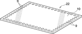
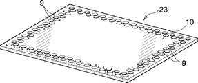
応力緩和部材(4)は高熱伝導性材料からなり、応力吸収空間を有している。図2に示すように、応力緩和部材(4)は、複数の非角形、ここでは円形貫通穴(9)が千鳥配置状に形成されたアルミニウム板(10)からなり、貫通穴(9)が応力吸収空間となっている。円形貫通穴(9)は、アルミニウム板(10)における少なくとも絶縁基板(3)の周縁部と対応する位置、すなわちアルミニウム板(10)における絶縁基板(3)の周縁部と対応する周縁部を含んで、全体に形成されている。アルミニウム板(10)は、熱伝導率が高く、ろう付時の加熱により強度が低下して変形能が高く、しかも溶融したろう材との濡れ性に優れた純度99%以上、望ましく純度99.5%以上の純アルミニウムにより形成されているのがよい。アルミニウム板(10)の肉厚は0.3〜3mmであることが好ましく、0.3〜1.5mmであることが望ましい。貫通穴(9)の円相当径、ここでは貫通穴(9)が円形であるから、その穴径は1〜4mmであることが好ましい。また、アルミニウム板(10)の一面の面積に対するすべての貫通穴(9)の面積の合計の割合が3〜50%の範囲内にあることが好ましい。 The stress relaxation member (4) is made of a high thermal conductivity material and has a stress absorption space. As shown in FIG. 2, the stress relaxation member (4) is composed of an aluminum plate (10) in which a plurality of non-square shapes, here circular through holes (9) are formed in a staggered arrangement, and the through holes (9) are formed. It is a stress absorption space. The circular through hole (9) includes at least a position corresponding to the peripheral edge of the insulating substrate (3) in the aluminum plate (10), that is, a peripheral edge corresponding to the peripheral edge of the insulating substrate (3) in the aluminum plate (10). And it is formed in the whole. The aluminum plate (10) has a high thermal conductivity, a strength that is reduced by heating during brazing, high deformability, and excellent wettability with the molten brazing material. It is good to be formed with 5% or more pure aluminum. The thickness of the aluminum plate (10) is preferably 0.3 to 3 mm, and more preferably 0.3 to 1.5 mm. Since the equivalent circular diameter of the through hole (9), here the through hole (9) is circular, the hole diameter is preferably 1 to 4 mm. Moreover, it is preferable that the ratio of the total area of all the through holes (9) to the area of one surface of the aluminum plate (10) is in the range of 3 to 50%.
ヒートシンク(5)は、複数の冷却流体通路(11)が並列状に設けられた偏平中空状であり、熱伝導性に優れるとともに、軽量であるアルミニウムにより形成されていることが好ましい。冷却流体としては、液体および気体のいずれを用いてもよい。 The heat sink (5) is preferably a flat hollow shape in which a plurality of cooling fluid passages (11) are provided in parallel, is excellent in thermal conductivity, and is preferably formed of lightweight aluminum. Either a liquid or a gas may be used as the cooling fluid.
応力緩和部材(4)と、パワーモジュール用基板(8)の金属層(7)およびヒートシンク(5)とのろう付は、たとえば次のようにして行われる。すなわち、応力緩和部材(4)を上記純アルミニウムからなる芯材と、芯材の両面を被覆するアルミニウムろう材製皮材とからなるアルミニウムブレージングシートにより形成する。なお、アルミニウムろう材としては、たとえばAl−Si系合金、Al−Si−Mg系合金などが用いられる。また、皮材の厚みは10〜200μm程度であることが好ましい。この厚みが薄すぎるとろう材の供給不足となってろう付不良を起こすおそれがあり、この厚みが厚すぎるとろう材過多となってボイドの発生や熱伝導性の低下を招くおそれがある。 The stress relaxation member (4), the metal layer (7) of the power module substrate (8), and the heat sink (5) are brazed, for example, as follows. That is, the stress relieving member (4) is formed by an aluminum brazing sheet comprising the core material made of the pure aluminum and the aluminum brazing material skin material covering both surfaces of the core material. As the aluminum brazing material, for example, an Al—Si alloy, an Al—Si—Mg alloy, or the like is used. The thickness of the skin material is preferably about 10 to 200 μm. If the thickness is too thin, the brazing material may be insufficiently supplied and brazing failure may occur, and if the thickness is too thick, the brazing material may become excessive and voids may be generated or the thermal conductivity may be reduced.
ついで、パワーモジュール用基板(8)、応力緩和部材(4)およびヒートシンク(5)を積層状に配置するとともに適当な治具により拘束し、接合面に適当な荷重を加えながら、真空雰囲気中または不活性ガス雰囲気中において、570〜600℃に加熱する。こうして、応力緩和部材(4)と、パワーモジュール用基板(8)の金属層(7)およびヒートシンク(5)とが同時にろう付される。 Next, the power module substrate (8), the stress relaxation member (4), and the heat sink (5) are arranged in a stack and restrained by an appropriate jig, while applying an appropriate load to the joint surface, in a vacuum atmosphere or Heat to 570-600 ° C in an inert gas atmosphere. Thus, the stress relaxation member (4), the metal layer (7) of the power module substrate (8), and the heat sink (5) are brazed simultaneously.
また、応力緩和部材(4)と、パワーモジュール用基板(8)の金属層(7)およびヒートシンク(5)とのろう付は、次のようにして行ってもよい。すなわち、応力緩和部材(4)を上記純アルミニウムのベア材により形成する。ついで、パワーモジュール用基板(8)、応力緩和部材(4)およびヒートシンク(5)を積層状に配置する。このとき、応力緩和部材(4)と、パワーモジュール用基板(8)の金属層(7)およびヒートシンク(5)との間に、それぞれAl−Si系合金、Al−Si−Mg系合金などからなるシート状アルミニウムろう材を介在させておく。シート状アルミニウムろう材の厚みは10〜200μm程度であることが好ましい。この厚みが薄すぎるとろう材の供給不足となってろう付不良を起こすおそれがあり、この厚みが厚すぎるとろう材過多となってボイドの発生や熱伝導性の低下を招くおそれがある。その後、上述したアルミニウムブレージングシートを用いた場合と同様にしてろう付する。こうして、応力緩和部材(4)と、パワーモジュール用基板(8)の金属層(7)およびヒートシンク(5)とが同時にろう付される。 The stress relaxation member (4), the metal layer (7) of the power module substrate (8), and the heat sink (5) may be brazed as follows. That is, the stress relieving member (4) is formed from the bare aluminum material. Next, the power module substrate (8), the stress relaxation member (4), and the heat sink (5) are arranged in a laminated form. At this time, between the stress relaxation member (4) and the metal layer (7) and the heat sink (5) of the power module substrate (8), respectively, an Al-Si alloy, an Al-Si-Mg alloy, etc. A sheet-like aluminum brazing material is interposed. The thickness of the sheet-like aluminum brazing material is preferably about 10 to 200 μm. If the thickness is too thin, the brazing material may be insufficiently supplied and brazing failure may occur, and if the thickness is too thick, the brazing material may become excessive and voids may be generated or the thermal conductivity may be reduced. Then, it brazes like the case where the aluminum brazing sheet mentioned above is used. Thus, the stress relaxation member (4), the metal layer (7) of the power module substrate (8), and the heat sink (5) are brazed simultaneously.
図3はこの発明による放熱装置の第2の実施形態を示す。 FIG. 3 shows a second embodiment of the heat dissipation device according to the present invention.
図3に示す放熱装置(15)の場合、パワーモジュール用基板(8)の絶縁基板(3)の下面には金属層(7)は形成されておらず、応力緩和部材(4)が絶縁基板(3)に直接ろう付されている。このろう付は、たとえば上記第1の実施形態の場合と同様にして行われる。 In the case of the heat dissipation device (15) shown in FIG. 3, the metal layer (7) is not formed on the lower surface of the insulating substrate (3) of the power module substrate (8), and the stress relaxation member (4) is the insulating substrate. It is brazed directly to (3). This brazing is performed, for example, in the same manner as in the first embodiment.
図4〜図21は応力緩和部材の変形例を示す。 4 to 21 show modified examples of the stress relaxation member.
図4に示す応力緩和部材(20)は、複数の方形貫通穴(21)が千鳥配置状に形成されたアルミニウム板(10)からなり、貫通穴(21)が応力吸収空間となっている。貫通穴(21)は、アルミニウム板(10)における少なくとも絶縁基板(3)の周縁部と対応する位置、すなわちアルミニウム板(10)における絶縁基板(3)の周縁部と対応する周縁部を含んで、全体に形成されている。アルミニウム板(10)の一面の面積に対するすべての貫通穴(21)の面積の合計の割合は、図2に示す応力緩和部材(4)の場合と同様に、3〜50%の範囲内にあることが好ましい。 The stress relaxation member (20) shown in FIG. 4 includes an aluminum plate (10) in which a plurality of rectangular through holes (21) are formed in a staggered arrangement, and the through holes (21) serve as stress absorbing spaces. The through hole (21) includes at least a position corresponding to the peripheral edge of the insulating substrate (3) in the aluminum plate (10), that is, a peripheral edge corresponding to the peripheral edge of the insulating substrate (3) in the aluminum plate (10). , Is formed throughout. The ratio of the total area of all the through holes (21) to the area of one surface of the aluminum plate (10) is in the range of 3 to 50% as in the case of the stress relaxation member (4) shown in FIG. It is preferable.
図5に示す応力緩和部材(22)の場合、アルミニウム板(10)の周縁部のみ、すなわちアルミニウム板(10)における絶縁基板(3)の周縁部と対応する位置のみに、複数の円形貫通穴(9)が形成されている。この場合にも、アルミニウム板(10)の一面の面積に対するすべての貫通穴(9)の面積の合計の割合は、図2に示す応力緩和部材(4)の場合と同様に、3〜50%の範囲内にあることが好ましい。 In the case of the stress relaxation member (22) shown in FIG. 5, a plurality of circular through-holes are formed only in the peripheral portion of the aluminum plate (10), that is, only in the position corresponding to the peripheral portion of the insulating substrate (3) in the aluminum plate (10). (9) is formed. Also in this case, the ratio of the total area of all the through holes (9) to the area of one surface of the aluminum plate (10) is 3 to 50% as in the case of the stress relaxation member (4) shown in FIG. It is preferable to be within the range.
図6に示す応力緩和部材(23)の場合、アルミニウム板(10)の周縁部のみ、すなわちアルミニウム板(10)における絶縁基板(3)の周縁部と対応する位置のみに、複数の円形貫通穴(9)が、内外2重に形成されている。この場合にも、アルミニウム板(10)の一面の面積に対するすべての貫通穴(9)の面積の合計の割合は、図2に示す応力緩和部材(4)の場合と同様に、3〜50%の範囲内にあることが好ましい。 In the case of the stress relieving member (23) shown in FIG. 6, a plurality of circular through holes are provided only at the peripheral edge of the aluminum plate (10), that is, only at the position corresponding to the peripheral edge of the insulating substrate (3) in the aluminum plate (10). (9) is formed in an inner and outer double. Also in this case, the ratio of the total area of all the through holes (9) to the area of one surface of the aluminum plate (10) is 3 to 50% as in the case of the stress relaxation member (4) shown in FIG. It is preferable to be within the range.
図5および図6に示す応力緩和部材(22)(23)において、円形貫通穴(9)の代わりに、方形貫通穴(21)が形成されていてもよい。いずれの場合においても、貫通穴(9)(21)が応力吸収空間となっている。 In the stress relaxation members (22) and (23) shown in FIGS. 5 and 6, a square through hole (21) may be formed instead of the circular through hole (9). In either case, the through holes (9) and (21) are stress absorbing spaces.
図7に示す応力緩和部材(25)は、一面に複数の球状凹所(26)が千鳥配置状に形成されたアルミニウム板(10)からなり、凹所(26)が応力吸収空間となっている。 The stress relaxation member (25) shown in FIG. 7 is composed of an aluminum plate (10) in which a plurality of spherical recesses (26) are formed in a staggered pattern on one surface, and the recess (26) serves as a stress absorption space. Yes.
図8に示す応力緩和部材(30)は、両面に複数の球状凹所(26)が千鳥配置状に形成されたアルミニウム板(10)からなり、凹所(26)が応力吸収空間となっている。アルミニウム板(10)の一面の凹所(26)と他面の凹所(26)とは、平面から見て異なった位置に形成されている。 The stress relaxation member (30) shown in FIG. 8 is composed of an aluminum plate (10) having a plurality of spherical recesses (26) formed on both sides in a staggered arrangement, and the recesses (26) serve as stress absorption spaces. Yes. The recess (26) on one surface of the aluminum plate (10) and the recess (26) on the other surface are formed at different positions when viewed from the plane.
図9に示す応力緩和部材(31)は、一面に複数の円錐台状凹所(32)が千鳥配置状に形成されたアルミニウム板(10)からなり、凹所(32)が応力吸収空間となっている。 The stress relieving member (31) shown in FIG. 9 is made of an aluminum plate (10) having a plurality of frustoconical recesses (32) formed in a staggered arrangement on one surface, and the recesses (32) are formed as stress absorption spaces. It has become.
図10に示す応力緩和部材(34)は、両面に複数の円錐台状凹所(32)が千鳥配置状に形成されたアルミニウム板(10)からなり、凹所(32)が応力吸収空間となっている。アルミニウム板(10)の一面の凹所(32)と他面の凹所(32)とは、平面から見て異なった位置に形成されている。 The stress relaxation member (34) shown in FIG. 10 includes an aluminum plate (10) in which a plurality of frustoconical recesses (32) are formed on both sides in a staggered arrangement, and the recesses (32) serve as stress absorption spaces. It has become. The recess (32) on one surface of the aluminum plate (10) and the recess (32) on the other surface are formed at different positions as viewed from the plane.
図7〜図10に示す応力緩和部材(25)(30)(31)(34)において、凹所(26)(32)は、アルミニウム板(10)における少なくとも絶縁基板(3)の周縁部と対応する周縁部を含んで、全体に形成されているが、図5および図6に示す応力緩和部材(22)(23)の場合と同様に、絶縁基板(3)の周縁部と対応する周縁部のみに形成されていればよい。また、図7〜図10に示す応力緩和部材(25)(30)(31)(34)において、凹所(26)(32)の開口の円相当径、ここでは凹所(26)(32)の開口は円形であるから、その直径は1〜4mmであることが好ましい。また、アルミニウム板(10)の凹所(26)(32)が形成された面の面積に対する当該面に形成された全凹所(26)(32)の開口面積の合計の割合が3〜50%の範囲内にあることが好ましい。 In the stress relaxation members (25), (30), (31), and (34) shown in FIGS. 7 to 10, the recesses (26) and (32) are at least the peripheral portion of the insulating substrate (3) in the aluminum plate (10). The peripheral edge corresponding to the peripheral edge of the insulating substrate (3) is formed as a whole including the corresponding peripheral edge, as in the case of the stress relaxation members (22) and (23) shown in FIGS. It suffices if it is formed only on the part. Further, in the stress relaxation members (25), (30), (31), and (34) shown in FIGS. 7 to 10, the equivalent circular diameter of the openings of the recesses (26) and (32), here, the recesses (26) and (32). ) Is circular, and the diameter is preferably 1 to 4 mm. Further, the ratio of the total opening area of all the recesses (26) (32) formed on the surface to the area of the surface of the aluminum plate (10) where the recesses (26) (32) are formed is 3 to 50. % Is preferably in the range of%.
図11に示す応力緩和部材(36)は、一面に複数の四角錐状凹所(37)が千鳥配置状に形成されたアルミニウム板(10)からなり、凹所(37)が応力吸収空間となっている。 The stress relaxation member (36) shown in FIG. 11 is composed of an aluminum plate (10) in which a plurality of quadrangular pyramid recesses (37) are formed in a staggered arrangement on one surface, and the recess (37) is formed as a stress absorption space. It has become.
図12に示す応力緩和部材(38)は、両面に複数の四角錐状凹所(37)が千鳥配置状に形成されたアルミニウム板(10)からなり、凹所(37)が応力吸収空間となっている。アルミニウム板(10)の一面の凹所(37)と他面の凹所(37)とは、平面から見て異なった位置に形成されている。 The stress relaxation member (38) shown in FIG. 12 includes an aluminum plate (10) in which a plurality of quadrangular pyramid recesses (37) are formed on both sides in a staggered arrangement, and the recess (37) is a stress absorption space. It has become. The recess (37) on one surface of the aluminum plate (10) and the recess (37) on the other surface are formed at different positions as viewed from the plane.
図13に示す応力緩和部材(40)は、一面に複数の直方体状凹所(41)が縦横に並んで形成されたアルミニウム板(10)からなり、凹所(41)が応力吸収空間となっている。ここでは、縦に並んだ凹所(41)の各列における隣り合う凹所(41)の長手方向は90度異なった方向を向いており、同じく横に並んだ凹所(41)の各列における隣り合う凹所(41)の長手方向は90度異なった方向を向いている。 The stress relaxation member (40) shown in FIG. 13 is composed of an aluminum plate (10) in which a plurality of rectangular parallelepiped recesses (41) are formed on one surface and arranged vertically and horizontally, and the recess (41) serves as a stress absorption space. ing. Here, the longitudinal direction of the adjacent recesses (41) in each row of the recesses (41) arranged in the vertical direction is different by 90 degrees, and each row of the recesses (41) also arranged in the horizontal direction The longitudinal direction of the adjacent recesses (41) in FIG.
図14に示す応力緩和部材(42)は、両面に複数の直方体状凹所(41)が千鳥配置状に形成されたアルミニウム板(10)からなり、凹所(41)が応力吸収空間となっている。アルミニウム板(10)の一面の凹所(41)と他面の凹所(41)とは、平面から見て異なった位置に形成されている。また、アルミニウム板(10)の一面の凹所(41)の長手方向は同方向を向いており、他面の凹所(41)の長手方向は、上記一面の凹所(41)の長手方向と直角をなす方向を向いている。 The stress relaxation member (42) shown in FIG. 14 includes an aluminum plate (10) in which a plurality of rectangular parallelepiped recesses (41) are formed on both sides in a staggered arrangement, and the recesses (41) serve as stress absorption spaces. ing. The recess (41) on one surface of the aluminum plate (10) and the recess (41) on the other surface are formed at different positions when viewed from the plane. The longitudinal direction of the recess (41) on one surface of the aluminum plate (10) faces the same direction, and the longitudinal direction of the recess (41) on the other surface is the longitudinal direction of the recess (41) on the one surface. It faces the direction that makes a right angle.
図15に示す応力緩和部材(45)は、複数の貫通穴(46)(47)が形成されたアルミニウム板(10)からなり、貫通穴(46)(47)が応力吸収空間となっている。すなわち、アルミニウム板(10)の4隅部においては、アルミニウム板(10)の各隅部を挟んで隣接する2つの辺を結ぶ傾斜した複数の平行線上に、それぞれ複数の短尺直線状貫通穴(46)が上記平行線の長さ方向に間隔をおいて形成されている。また、アルミニウム板(10)の4隅部を除いた部分においては、複数の同心円上に、それぞれ複数の円弧状貫通穴(47)が周方向に間隔をおいて形成されている。この応力緩和部材(45)の場合も、アルミニウム板(10)の一面の面積に対するすべての貫通穴(46)(47)の面積の合計の割合が3〜50%の範囲内にあることが好ましい。 The stress relaxation member (45) shown in FIG. 15 includes an aluminum plate (10) having a plurality of through holes (46) and (47), and the through holes (46) and (47) serve as stress absorbing spaces. . That is, at the four corners of the aluminum plate (10), a plurality of short straight through holes (each having a plurality of inclined parallel lines connecting two adjacent sides across each corner of the aluminum plate (10) are provided. 46) are formed at intervals in the length direction of the parallel lines. Further, in the portion excluding the four corners of the aluminum plate (10), a plurality of arc-shaped through holes (47) are formed on the plurality of concentric circles at intervals in the circumferential direction. Also in the case of this stress relaxation member (45), the ratio of the total area of all the through holes (46) and (47) to the area of one surface of the aluminum plate (10) is preferably in the range of 3 to 50%. .
図16に示す応力緩和部材(50)は、一面に複数の溝状凹所(51)が形成されたアルミニウム板(10)からなり、凹所(51)が応力吸収空間となっている。凹所(51)はV字を連続したような形状またはV字状である。 The stress relaxation member (50) shown in FIG. 16 is made of an aluminum plate (10) having a plurality of groove-like recesses (51) formed on one surface, and the recesses (51) serve as stress absorption spaces. The recess (51) is shaped like a continuous V or V shape.
図17に示す応力緩和部材(53)は、両面に複数のV溝状凹所(54)(55)が形成されたアルミニウム板(10)からなり、凹所(54)(55)が応力吸収空間となっている。アルミニウム板(10)の一面の凹所(54)は、アルミニウム板(10)の長さ方向に伸びかつアルミニウム板(10)の幅方向に間隔をおいて形成されている。アルミニウム板(10)の他面の凹所(55)は、アルミニウム板(10)の幅方向に伸びかつアルミニウム板(10)の長さ方向に間隔をおいて形成されている。なお、アルミニウム板(10)の一面の凹所(54)の深さと他面の凹所(55)の深さの合計は、アルミニウム板(10)の板厚よりも小さくなっている。 The stress relaxation member (53) shown in FIG. 17 is composed of an aluminum plate (10) having a plurality of V-groove recesses (54) and (55) formed on both surfaces, and the recesses (54) and (55) absorb stress. It is a space. The recesses (54) on one surface of the aluminum plate (10) extend in the length direction of the aluminum plate (10) and are spaced apart in the width direction of the aluminum plate (10). The recesses (55) on the other surface of the aluminum plate (10) extend in the width direction of the aluminum plate (10) and are spaced apart in the length direction of the aluminum plate (10). The sum of the depth of the recess (54) on one surface of the aluminum plate (10) and the depth of the recess (55) on the other surface is smaller than the thickness of the aluminum plate (10).
図18に示す応力緩和部材(57)は、両面に複数のV溝状凹所(58)(59)が形成されるとともに、複数の貫通穴(60)が形成されたアルミニウム板(10)からなり、凹所(58)(59)および貫通穴(60)が応力吸収空間となっている。アルミニウム板(10)の一面の凹所(58)は、アルミニウム板(10)の長さ方向に伸びかつアルミニウム板(10)の幅方向に間隔をおいて形成されている。アルミニウム板(10)の他面の凹所(59)は、アルミニウム板(10)の幅方向に伸びかつアルミニウム板(10)の長さ方向に間隔をおいて形成されている。そして、アルミニウム板(10)の一面の凹所(58)の深さと他面の凹所(59)の深さの合計は、アルミニウム板(10)の板厚よりも大きくなっており、これにより両凹所(58)(59)の交差部分に貫通穴(60)が形成されている。 The stress relaxation member (57) shown in FIG. 18 is formed from an aluminum plate (10) in which a plurality of V-groove recesses (58) and (59) are formed on both surfaces and a plurality of through holes (60) are formed. Thus, the recesses (58) and (59) and the through hole (60) are stress absorption spaces. The recesses (58) on one surface of the aluminum plate (10) extend in the length direction of the aluminum plate (10) and are spaced apart in the width direction of the aluminum plate (10). The recesses (59) on the other surface of the aluminum plate (10) extend in the width direction of the aluminum plate (10) and are spaced apart in the length direction of the aluminum plate (10). The sum of the depth of the recess (58) on one surface of the aluminum plate (10) and the depth of the recess (59) on the other surface is larger than the thickness of the aluminum plate (10), thereby A through hole (60) is formed at the intersection of the two recesses (58) and (59).
図4〜図18に示す応力緩和部材を形成するアルミニウム板(10)は、図2に示す応力緩和部材(4)の場合と同じである。そして、図4〜図18に示す応力緩和部材は、上述した第1および第2の実施形態の場合と同様にして、パワーモジュール用基板(8)およびヒートシンク(5)にろう付される。 The aluminum plate (10) forming the stress relaxation member shown in FIGS. 4 to 18 is the same as the case of the stress relaxation member (4) shown in FIG. The stress relaxation member shown in FIGS. 4 to 18 is brazed to the power module substrate (8) and the heat sink (5) in the same manner as in the first and second embodiments described above.
図19に示す応力緩和部材(63)は、波頂部(64)、波底部(65)および波頂部(64)と波底部(65)とを連結する連結部(66)とよりなる波形のアルミニウム板(67)からなり、隣り合う連結部(66)どうしの間の部分が応力吸収空間となっている。また、波形アルミニウム板(67)の幅方向の中央部において、波頂部(64)、波底部(65)および連結部(66)に、波頂部(64)および波底部(65)の長さ方向と直交する方向に伸びる切除部(68)が形成されている。したがって、波形アルミニウム板(67)は、両端部を除いて2つの部分に分割されている。 The stress relieving member (63) shown in FIG. 19 includes corrugated aluminum composed of a wave crest (64), a wave bottom (65), and a connecting part (66) connecting the wave crest (64) and the wave bottom (65). It consists of a board (67), and the part between adjacent connection parts (66) is a stress absorption space. Further, in the center portion of the corrugated aluminum plate (67) in the width direction, the wave crest portion (64), the wave bottom portion (65) and the connecting portion (66) are connected to the wave crest portion (64) and the wave bottom portion (65) in the length direction. A cut-out portion (68) extending in a direction orthogonal to is formed. Therefore, the corrugated aluminum plate (67) is divided into two parts except for both ends.
図20に示す応力緩和部材(70)は、図19と同様な波形アルミニウム板(67)の波頂部(64)、波底部(65)および連結部(66)に、波頂部(64)および波底部(65)の長さ方向と直交する方向に伸びる切除部(68)が、波形アルミニウム板(67)の幅方向に並んで複数形成されている。したがって、波形アルミニウム板(67)は、両端部を除いて複数の部分に分割されている。 The stress relieving member (70) shown in FIG. 20 has a wave crest (64) and a wave at the wave crest (64), wave bottom (65) and connection (66) of a corrugated aluminum plate (67) similar to FIG. A plurality of cut portions (68) extending in the direction perpendicular to the length direction of the bottom portion (65) are formed side by side in the width direction of the corrugated aluminum plate (67). Therefore, the corrugated aluminum plate (67) is divided into a plurality of portions except for both ends.
図21に示す応力緩和部材(72)は、切除部が形成されていない複数、ここでは2つの波形アルミニウム板(67)が、波頂部(64)および波底部(65)の長さ方向に間隔をおいて配置されている。なお、波形アルミニウム板(67)の数は限定されない。そして、隣り合う波形アルミニウム板(67)の波頂部(64)および波底部(65)の位置が、波頂部(64)および波底部(65)の幅方向にずれている。 In the stress relaxation member (72) shown in FIG. 21, a plurality of, in this case, two corrugated aluminum plates (67) with no cut portions formed are spaced in the length direction of the wave crest (64) and the wave bottom (65). Is placed. The number of corrugated aluminum plates (67) is not limited. Then, the positions of the wave crest (64) and the wave bottom (65) of the adjacent corrugated aluminum plates (67) are shifted in the width direction of the wave crest (64) and the wave bottom (65).
なお、図21に示す応力緩和部材(72)において、隣り合う波形アルミニウム板(67)の波頂部(64)および波底部(65)の位置が、波頂部(64)および波底部(65)の幅方向にずれていない場合もある。 In the stress relaxation member (72) shown in FIG. 21, the positions of the wave crest (64) and the wave bottom (65) of the adjacent corrugated aluminum plates (67) are the positions of the wave crest (64) and the wave bottom (65). In some cases, it is not shifted in the width direction.
図19〜図21に示す応力緩和部材(63)(70)(72)において、波形アルミニウム板(67)の肉厚は0.05〜1mmであることが好ましい。また、波形アルミニウム板(67)は、図2に示す応力緩和部材(4)の場合と同様に、熱伝導率が高く、しかもろう付時の加熱により強度が低下して変形能の高い純度99%以上、望ましく純度99.5%以上の純アルミニウムにより形成されているのがよい。図19〜図21に示す応力緩和部材(63)(70)(72)は、上述した第1および第2の実施形態の場合と同様にして、パワーモジュール用基板(8)およびヒートシンク(5)にろう付される。 In the stress relaxation members (63), (70) and (72) shown in FIGS. 19 to 21, the thickness of the corrugated aluminum plate (67) is preferably 0.05 to 1 mm. Further, the corrugated aluminum plate (67) has a high thermal conductivity, as in the case of the stress relaxation member (4) shown in FIG. % Or more, preferably 99.5% or more pure aluminum. The stress relieving members (63), (70), (72) shown in FIGS. 19 to 21 are the same as in the first and second embodiments described above, and the power module substrate (8) and the heat sink (5). Brazed.
(1)(15):放熱装置
(3):絶縁基板
(4):応力緩和部材
(5):ヒートシンク
(7):金属層
(9):貫通穴
(10):アルミニウム板
(20)(22)(23):応力緩和部材
(21):貫通穴
(25)(30):応力緩和部材
(26):凹所
(31)(34):応力緩和部材
(32):凹所
(36)(38):応力緩和部材
(37):凹所
(40)(42):応力緩和部材
(41):凹所
(45):応力緩和部材
(46)(47):貫通穴
(50)(53)(57):応力緩和部材
(51)(54)(55)(58)(59):凹所
(60):貫通穴
(63)(70)(72):応力緩和部材
(64):波頂部
(65):波底部
(66):連結部
(67):波形アルミニウム板
(68):切除部
(1) (15): Heat dissipation device
(3): Insulating substrate
(4): Stress relaxation member
(5): Heat sink
(7): Metal layer
(9): Through hole
(10): Aluminum plate
(20) (22) (23): Stress relaxation member
(21): Through hole
(25) (30): Stress relaxation member
(26): Recess
(31) (34): Stress relief member
(32): Recess
(36) (38): Stress relief member
(37): Recess
(40) (42): Stress relief member
(41): Recess
(45): Stress relaxation member
(46) (47): Through hole
(50) (53) (57): Stress relaxation member
(51) (54) (55) (58) (59): Recess
(60): Through hole
(63) (70) (72): Stress relaxation member
(64): Wave peak
(65): Wave bottom
(66): Connecting part
(67): Corrugated aluminum plate
(68): Resected part
Claims (11)
ヒートシンクに冷却流体通路が設けられ、応力緩和部材が、複数の貫通穴が形成された肉厚0.3〜3mmのアルミニウム板からなるとともに、貫通穴が応力吸収空間となっており、応力緩和部材が、絶縁基板およびヒートシンクにろう付されている放熱装置。 In a heat dissipation device comprising an insulating substrate whose one surface is a heating element mounting surface, a heat sink fixed to the other surface of the insulating substrate, and a stress relaxation member interposed between the insulating substrate and the heat sink ,
A cooling fluid passage is provided in the heat sink, and the stress relaxation member is made of an aluminum plate having a thickness of 0.3 to 3 mm in which a plurality of through holes are formed, and the through hole is a stress absorption space. Is a heat dissipation device brazed to an insulating substrate and a heat sink.
Priority Applications (7)
| Application Number | Priority Date | Filing Date | Title |
|---|---|---|---|
| JP2005110175A JP4621531B2 (en) | 2005-04-06 | 2005-04-06 | Heat dissipation device |
| US11/910,460 US20090139704A1 (en) | 2005-04-06 | 2006-04-06 | Heat sink device |
| EP15150109.5A EP2863425A3 (en) | 2005-04-06 | 2006-04-06 | Heat radiator |
| PCT/JP2006/307307 WO2006109660A1 (en) | 2005-04-06 | 2006-04-06 | Heat sink device |
| KR1020077025597A KR101242286B1 (en) | 2005-04-06 | 2006-04-06 | Heat sink device |
| CN2006800113253A CN101156241B (en) | 2005-04-06 | 2006-04-06 | Heat sink device |
| EP06731255.3A EP1873827B1 (en) | 2005-04-06 | 2006-04-06 | Heat radiating device |
Applications Claiming Priority (1)
| Application Number | Priority Date | Filing Date | Title |
|---|---|---|---|
| JP2005110175A JP4621531B2 (en) | 2005-04-06 | 2005-04-06 | Heat dissipation device |
Related Child Applications (1)
| Application Number | Title | Priority Date | Filing Date |
|---|---|---|---|
| JP2010188114A Division JP5282075B2 (en) | 2010-08-25 | 2010-08-25 | Heat dissipation device |
Publications (3)
| Publication Number | Publication Date |
|---|---|
| JP2006294699A JP2006294699A (en) | 2006-10-26 |
| JP2006294699A5 JP2006294699A5 (en) | 2007-08-30 |
| JP4621531B2 true JP4621531B2 (en) | 2011-01-26 |
Family
ID=37086936
Family Applications (1)
| Application Number | Title | Priority Date | Filing Date |
|---|---|---|---|
| JP2005110175A Expired - Fee Related JP4621531B2 (en) | 2005-04-06 | 2005-04-06 | Heat dissipation device |
Country Status (6)
| Country | Link |
|---|---|
| US (1) | US20090139704A1 (en) |
| EP (2) | EP1873827B1 (en) |
| JP (1) | JP4621531B2 (en) |
| KR (1) | KR101242286B1 (en) |
| CN (1) | CN101156241B (en) |
| WO (1) | WO2006109660A1 (en) |
Cited By (1)
| Publication number | Priority date | Publication date | Assignee | Title |
|---|---|---|---|---|
| US10276475B2 (en) | 2012-12-26 | 2019-04-30 | Kabushiki Kaisha Toyota Chuo Kenkyusho | Thermal conductive stress relaxation structure |
Families Citing this family (85)
| Publication number | Priority date | Publication date | Assignee | Title |
|---|---|---|---|---|
| JP4604954B2 (en) * | 2005-10-13 | 2011-01-05 | 株式会社デンソー | Insulation structure of semiconductor module |
| EP2003691B1 (en) | 2006-03-13 | 2019-01-09 | Showa Denko K.K. | Base for power module |
| JP5064111B2 (en) * | 2006-06-28 | 2012-10-31 | 株式会社ティラド | Composite heat dissipation plate, method for manufacturing the same, and thermal stress relaxation plate used therefor |
| KR100798474B1 (en) | 2006-11-22 | 2008-01-28 | 한국표준과학연구원 | Semiconductor chip with dopped conducting layer and metal layer |
| JP4752785B2 (en) * | 2007-02-15 | 2011-08-17 | 三菱マテリアル株式会社 | Manufacturing method of power module substrate with heat sink |
| DE102007019885B4 (en) | 2007-04-27 | 2010-11-25 | Wieland-Werke Ag | Heatsink with matrix-structured surface |
| JP2008294281A (en) * | 2007-05-25 | 2008-12-04 | Showa Denko Kk | Semiconductor device and manufacturing method therefor |
| JP4945319B2 (en) | 2007-05-25 | 2012-06-06 | 昭和電工株式会社 | Semiconductor device |
| JP2008294279A (en) | 2007-05-25 | 2008-12-04 | Showa Denko Kk | Semiconductor device |
| JP4867793B2 (en) * | 2007-05-25 | 2012-02-01 | 株式会社豊田自動織機 | Semiconductor device |
| JP2009130060A (en) * | 2007-11-21 | 2009-06-11 | Toyota Industries Corp | Heat dissipater |
| JP5070014B2 (en) * | 2007-11-21 | 2012-11-07 | 株式会社豊田自動織機 | Heat dissipation device |
| JP4832419B2 (en) * | 2007-12-25 | 2011-12-07 | トヨタ自動車株式会社 | Semiconductor module |
| JP5011088B2 (en) * | 2007-12-26 | 2012-08-29 | 日新製鋼株式会社 | Heat dissipation device and power module |
| KR101463075B1 (en) * | 2008-02-04 | 2014-11-20 | 페어차일드코리아반도체 주식회사 | Heat sink package |
| JP4380774B2 (en) * | 2008-03-19 | 2009-12-09 | トヨタ自動車株式会社 | Power module |
| TWI501360B (en) * | 2008-04-17 | 2015-09-21 | Samsung Electronics Co Ltd | Tape for heat dissipating member, chip on film type semiconductor package including heat dissipating member, and electronic apparatus including the same |
| JP4989552B2 (en) | 2008-05-08 | 2012-08-01 | トヨタ自動車株式会社 | Electronic components |
| JP5114323B2 (en) * | 2008-07-04 | 2013-01-09 | 株式会社豊田自動織機 | Semiconductor device |
| US8472193B2 (en) * | 2008-07-04 | 2013-06-25 | Kabushiki Kaisha Toyota Jidoshokki | Semiconductor device |
| JP5114324B2 (en) * | 2008-07-07 | 2013-01-09 | 株式会社豊田自動織機 | Semiconductor device |
| JP5227681B2 (en) * | 2008-07-11 | 2013-07-03 | 株式会社豊田自動織機 | Semiconductor device |
| EP2166569A1 (en) * | 2008-09-22 | 2010-03-24 | ABB Schweiz AG | Cooling device for a power component |
| JP2010171279A (en) * | 2009-01-23 | 2010-08-05 | Toyota Motor Corp | Heat radiator |
| JP5261214B2 (en) * | 2009-01-29 | 2013-08-14 | 住友軽金属工業株式会社 | Method for manufacturing aluminum clad material for heat generating component cooling device |
| DE102009000514A1 (en) | 2009-01-30 | 2010-08-26 | Robert Bosch Gmbh | Composite component and method for producing a composite component |
| TW201041496A (en) * | 2009-05-15 | 2010-11-16 | High Conduction Scient Co Ltd | A manufacturing method of circuit board module equipped with heat sink, and its product |
| CN102804368B (en) * | 2009-06-10 | 2015-12-02 | 丰田自动车株式会社 | Semiconductor device |
| CN101929819A (en) * | 2009-06-26 | 2010-12-29 | 富准精密工业(深圳)有限公司 | Flat-plate heat pipe |
| JP2011023545A (en) * | 2009-07-15 | 2011-02-03 | Nisshin Steel Co Ltd | Heat dissipation structure and power module |
| JP5700034B2 (en) | 2009-08-10 | 2015-04-15 | 富士電機株式会社 | Semiconductor module and cooler |
| DE102009042519A1 (en) * | 2009-09-16 | 2011-03-24 | Esw Gmbh | Device for cooling semiconductors |
| CN102574361B (en) * | 2009-11-27 | 2015-08-19 | 昭和电工株式会社 | Laminate and manufacture method thereof |
| JP5515947B2 (en) * | 2010-03-29 | 2014-06-11 | 株式会社豊田自動織機 | Cooling system |
| US20110240280A1 (en) * | 2010-03-31 | 2011-10-06 | Kabushiki Kaisha Kobe Seiko Sho (Kobe Steel, Ltd.) | Aluminum alloy brazing sheet and heat exchanger |
| JP2011228563A (en) * | 2010-04-22 | 2011-11-10 | Showa Denko Kk | Method of brazing insulating laminate material |
| US9379038B2 (en) | 2010-04-28 | 2016-06-28 | Kabushiki Kaisha Toyota Jidoshokki | Heat dissipation device and semiconductor device |
| JP5613452B2 (en) * | 2010-05-19 | 2014-10-22 | 昭和電工株式会社 | Brazing method for insulating laminates |
| JP5382049B2 (en) * | 2010-06-30 | 2014-01-08 | 株式会社デンソー | Semiconductor device |
| US8587116B2 (en) * | 2010-09-30 | 2013-11-19 | Infineon Technologies Ag | Semiconductor module comprising an insert |
| JP5671351B2 (en) * | 2011-01-12 | 2015-02-18 | 昭和電工株式会社 | Manufacturing method of electronic device mounting substrate |
| JP2012169319A (en) * | 2011-02-10 | 2012-09-06 | Showa Denko Kk | Insulation laminate material, insulation circuit board, base for power module, and power module |
| JP5764342B2 (en) * | 2011-02-10 | 2015-08-19 | 昭和電工株式会社 | Insulated circuit board, power module base and manufacturing method thereof |
| JP5349572B2 (en) | 2011-04-18 | 2013-11-20 | 株式会社豊田自動織機 | Radiator and method of manufacturing radiator |
| JP5234138B2 (en) * | 2011-05-06 | 2013-07-10 | 船井電機株式会社 | Heat sink |
| JP5913834B2 (en) * | 2011-05-16 | 2016-04-27 | 昭和電工株式会社 | Brazing filler metal foil for heat dissipation devices |
| DE102012208767A1 (en) * | 2011-06-17 | 2012-12-20 | Robert Bosch Gmbh | Electronic circuit with loss of heat emitting components |
| JP2013038123A (en) * | 2011-08-04 | 2013-02-21 | Showa Denko Kk | Method for manufacturing insulation circuit board |
| US20130056176A1 (en) * | 2011-08-26 | 2013-03-07 | Mikros Manufacturing, Inc. | Heat Exchanger with Controlled Coefficient of Thermal Expansion |
| JP2013115201A (en) * | 2011-11-28 | 2013-06-10 | Toyota Industries Corp | Semiconductor device |
| WO2013089099A1 (en) * | 2011-12-12 | 2013-06-20 | 三菱マテリアル株式会社 | Power module substrate, substrate for power module with heat sink, power module, paste for forming flux component penetration prevention layer, and bonding method for article to be bonded |
| JP5856838B2 (en) * | 2011-12-22 | 2016-02-10 | 昭和電工株式会社 | Brazing filler metal foil for heat dissipation devices |
| JP5990925B2 (en) * | 2012-02-16 | 2016-09-14 | 富士通株式会社 | Cooling device and manufacturing method thereof |
| JP5969235B2 (en) * | 2012-03-23 | 2016-08-17 | 昭和電工株式会社 | Aluminum clad material for heat exchanger and manufacturing method thereof |
| JP6060553B2 (en) * | 2012-04-06 | 2017-01-18 | 株式会社豊田自動織機 | Semiconductor device |
| KR101499665B1 (en) * | 2012-05-29 | 2015-03-06 | 포리프라스틱 가부시키가이샤 | Method for manufacturing composite molded article |
| JP2014017318A (en) * | 2012-07-06 | 2014-01-30 | Toyota Industries Corp | Semiconductor device |
| JP2014072314A (en) * | 2012-09-28 | 2014-04-21 | Toyota Industries Corp | Semiconductor device and semiconductor device manufacturing method |
| JP5708613B2 (en) * | 2012-11-01 | 2015-04-30 | 株式会社豊田自動織機 | module |
| JP6197329B2 (en) * | 2013-03-28 | 2017-09-20 | 三菱マテリアル株式会社 | Power module and method of manufacturing thermal interface plate |
| JP5648705B2 (en) * | 2013-04-08 | 2015-01-07 | 三菱マテリアル株式会社 | Power module substrate with heat sink, power module with heat sink and power module substrate with buffer layer |
| JP6197365B2 (en) * | 2013-05-21 | 2017-09-20 | 三菱マテリアル株式会社 | Power module and method of manufacturing thermal interface plate |
| JP6116404B2 (en) * | 2013-07-01 | 2017-04-19 | 昭和電工株式会社 | Heat dissipation device |
| DE102013218826A1 (en) * | 2013-09-19 | 2015-03-19 | Siemens Aktiengesellschaft | heatsink |
| WO2015045648A1 (en) * | 2013-09-30 | 2015-04-02 | 富士電機株式会社 | Semiconductor device, method for assembling semiconductor device, component for semiconductor devices and unit module |
| KR101534744B1 (en) * | 2013-12-16 | 2015-07-24 | 현대자동차 주식회사 | Cooling system for diesel engine having turbo charger |
| JP6316219B2 (en) * | 2015-01-22 | 2018-04-25 | 三菱電機株式会社 | Power semiconductor module |
| US10510640B2 (en) | 2015-01-26 | 2019-12-17 | Miitsubishi Electric Corporation | Semiconductor device and method for manufacturing semiconductor device |
| US20160229689A1 (en) * | 2015-02-11 | 2016-08-11 | Analog Devices, Inc. | Packaged Microchip with Patterned Interposer |
| CN107429976B (en) * | 2015-03-16 | 2021-02-09 | 达纳加拿大公司 | Heat exchanger with plate having surface pattern for improving flatness and method of manufacturing the same |
| JP6805743B2 (en) * | 2015-12-24 | 2020-12-23 | アイシン精機株式会社 | Insulated substrate |
| JP6549502B2 (en) * | 2016-02-26 | 2019-07-24 | 京セラ株式会社 | Heat dissipation substrate, semiconductor package and semiconductor module using the same |
| DE102016218522B3 (en) * | 2016-09-27 | 2017-06-22 | Jenoptik Laser Gmbh | Optical or optoelectronic assembly and method of making the same |
| DE102017203217A1 (en) * | 2017-02-28 | 2018-08-30 | Robert Bosch Gmbh | Contact configuration |
| US11276617B2 (en) * | 2017-11-28 | 2022-03-15 | Kyocera Corporation | Electronic device mounting board, electronic package, and electronic module |
| CN108337862B (en) * | 2018-03-02 | 2019-09-06 | 惠州市博宇科技有限公司 | A kind of new energy electric motor vehicle special-purpose aluminum substrate |
| EP3595105B1 (en) * | 2018-07-13 | 2024-01-24 | ABB Schweiz AG | A heat sink for a high voltage switchgear |
| US10490482B1 (en) * | 2018-12-05 | 2019-11-26 | Toyota Motor Engineering & Manufacturing North America, Inc. | Cooling devices including jet cooling with an intermediate mesh and methods for using the same |
| JP7367309B2 (en) * | 2019-02-08 | 2023-10-24 | 富士電機株式会社 | Semiconductor module, semiconductor device, and method for manufacturing semiconductor device |
| JP2020141023A (en) * | 2019-02-27 | 2020-09-03 | 株式会社 日立パワーデバイス | Semiconductor device |
| US11217505B2 (en) * | 2019-09-10 | 2022-01-04 | Aptiv Technologies Limited | Heat exchanger for electronics |
| CN110634822A (en) * | 2019-10-08 | 2019-12-31 | 广东美的制冷设备有限公司 | Mounting substrate, intelligent power module and air conditioner |
| CN210959284U (en) * | 2019-12-06 | 2020-07-07 | 阳光电源股份有限公司 | Radiator and electrical equipment |
| CN112318790B (en) * | 2020-09-09 | 2022-08-19 | 西安近代化学研究所 | Vulcanization molding process for high-viscosity silicon-based heat insulation layer |
| DE102021201270A1 (en) * | 2021-02-10 | 2022-08-11 | Vitesco Technologies GmbH | Electronic assembly with at least a first electronic component and a second electronic component |
Citations (4)
| Publication number | Priority date | Publication date | Assignee | Title |
|---|---|---|---|---|
| JPH0883872A (en) * | 1994-09-09 | 1996-03-26 | Kyocera Corp | Package for semiconductor element |
| JP2000236050A (en) * | 1999-02-12 | 2000-08-29 | Sony Corp | Heat radiator, electronic apparatus and spacer for heat radiator |
| JP2002237556A (en) * | 2001-02-09 | 2002-08-23 | Mitsubishi Electric Corp | Power semiconductor device |
| JP2003017627A (en) * | 2001-06-28 | 2003-01-17 | Toshiba Corp | Ceramic circuit board and semiconductor module using the same |
Family Cites Families (22)
| Publication number | Priority date | Publication date | Assignee | Title |
|---|---|---|---|---|
| JPH0612795B2 (en) * | 1989-11-07 | 1994-02-16 | 株式会社日立製作所 | Multi-chip module cooling structure |
| JP2675173B2 (en) * | 1990-03-02 | 1997-11-12 | 株式会社日立製作所 | Electronic device cooling system |
| JPH05299549A (en) * | 1992-04-20 | 1993-11-12 | Hitachi Ltd | Heat transfer cooling device |
| JP3401089B2 (en) * | 1994-09-09 | 2003-04-28 | 京セラ株式会社 | Package for storing semiconductor elements |
| JPH10189845A (en) * | 1996-12-25 | 1998-07-21 | Denso Corp | Heat sink for semiconductor device |
| US6124635A (en) * | 1997-03-21 | 2000-09-26 | Honda Giken Kogyo Kabushiki Kaisha | Functionally gradient integrated metal-ceramic member and semiconductor circuit substrate application thereof |
| US5988488A (en) * | 1997-09-02 | 1999-11-23 | Mcdonnell Douglas Corporation | Process of bonding copper and tungsten |
| US6756019B1 (en) * | 1998-02-24 | 2004-06-29 | Caliper Technologies Corp. | Microfluidic devices and systems incorporating cover layers |
| JP4649027B2 (en) * | 1999-09-28 | 2011-03-09 | 株式会社東芝 | Ceramic circuit board |
| EP1122780A3 (en) * | 2000-01-31 | 2004-01-02 | Ngk Insulators, Ltd. | Laminated radiation member, power semiconductor apparatus and method for producing the same |
| WO2002067324A1 (en) * | 2001-02-22 | 2002-08-29 | Ngk Insulators, Ltd. | Member for electronic circuit, method for manufacturing the member, and electronic part |
| US20020185726A1 (en) * | 2001-06-06 | 2002-12-12 | North Mark T. | Heat pipe thermal management of high potential electronic chip packages |
| JP3793562B2 (en) * | 2001-09-27 | 2006-07-05 | 京セラ株式会社 | Ceramic circuit board |
| JP2003101184A (en) * | 2001-09-27 | 2003-04-04 | Kyocera Corp | Ceramic circuit board and production method therefor |
| JP2003163315A (en) * | 2001-11-29 | 2003-06-06 | Denki Kagaku Kogyo Kk | Module |
| JP2004153075A (en) | 2002-10-31 | 2004-05-27 | Mitsubishi Materials Corp | Substrate for power module and power module |
| JP4044449B2 (en) * | 2003-01-30 | 2008-02-06 | 株式会社住友金属エレクトロデバイス | Power module substrate |
| US6903929B2 (en) * | 2003-03-31 | 2005-06-07 | Intel Corporation | Two-phase cooling utilizing microchannel heat exchangers and channeled heat sink |
| DE10337640A1 (en) * | 2003-08-16 | 2005-03-17 | Semikron Elektronik Gmbh | Power semiconductor module for fitting on a heat sink has a casing, power semiconductor components and an insulating substrate with metal layers on both sides |
| KR100542188B1 (en) * | 2003-08-26 | 2006-01-10 | 삼성에스디아이 주식회사 | Plasma display device |
| JP4617209B2 (en) * | 2005-07-07 | 2011-01-19 | 株式会社豊田自動織機 | Heat dissipation device |
| US8472193B2 (en) * | 2008-07-04 | 2013-06-25 | Kabushiki Kaisha Toyota Jidoshokki | Semiconductor device |
-
2005
- 2005-04-06 JP JP2005110175A patent/JP4621531B2/en not_active Expired - Fee Related
-
2006
- 2006-04-06 KR KR1020077025597A patent/KR101242286B1/en not_active IP Right Cessation
- 2006-04-06 US US11/910,460 patent/US20090139704A1/en not_active Abandoned
- 2006-04-06 WO PCT/JP2006/307307 patent/WO2006109660A1/en active Application Filing
- 2006-04-06 EP EP06731255.3A patent/EP1873827B1/en active Active
- 2006-04-06 EP EP15150109.5A patent/EP2863425A3/en not_active Withdrawn
- 2006-04-06 CN CN2006800113253A patent/CN101156241B/en not_active Expired - Fee Related
Patent Citations (4)
| Publication number | Priority date | Publication date | Assignee | Title |
|---|---|---|---|---|
| JPH0883872A (en) * | 1994-09-09 | 1996-03-26 | Kyocera Corp | Package for semiconductor element |
| JP2000236050A (en) * | 1999-02-12 | 2000-08-29 | Sony Corp | Heat radiator, electronic apparatus and spacer for heat radiator |
| JP2002237556A (en) * | 2001-02-09 | 2002-08-23 | Mitsubishi Electric Corp | Power semiconductor device |
| JP2003017627A (en) * | 2001-06-28 | 2003-01-17 | Toshiba Corp | Ceramic circuit board and semiconductor module using the same |
Cited By (1)
| Publication number | Priority date | Publication date | Assignee | Title |
|---|---|---|---|---|
| US10276475B2 (en) | 2012-12-26 | 2019-04-30 | Kabushiki Kaisha Toyota Chuo Kenkyusho | Thermal conductive stress relaxation structure |
Also Published As
| Publication number | Publication date |
|---|---|
| WO2006109660A1 (en) | 2006-10-19 |
| CN101156241A (en) | 2008-04-02 |
| KR101242286B1 (en) | 2013-03-12 |
| JP2006294699A (en) | 2006-10-26 |
| EP2863425A2 (en) | 2015-04-22 |
| EP1873827B1 (en) | 2020-09-09 |
| CN101156241B (en) | 2010-05-19 |
| EP1873827A4 (en) | 2014-01-01 |
| EP1873827A1 (en) | 2008-01-02 |
| KR20080002925A (en) | 2008-01-04 |
| EP2863425A3 (en) | 2015-08-19 |
| US20090139704A1 (en) | 2009-06-04 |
Similar Documents
| Publication | Publication Date | Title |
|---|---|---|
| JP4621531B2 (en) | Heat dissipation device | |
| JP4617209B2 (en) | Heat dissipation device | |
| JP4867793B2 (en) | Semiconductor device | |
| JP4945319B2 (en) | Semiconductor device | |
| JP5007296B2 (en) | Power module base | |
| EP2224484A1 (en) | Semiconductor module | |
| JP2010171279A (en) | Heat radiator | |
| JP5282075B2 (en) | Heat dissipation device | |
| JP2007299798A (en) | Ceramic substrate having heat sink | |
| JP2008124187A (en) | Base for power module | |
| JP2008124187A6 (en) | Power module base | |
| JP6738193B2 (en) | Heat transfer structure, insulating laminated material, insulating circuit board and power module base | |
| JP6316219B2 (en) | Power semiconductor module | |
| JP2008016598A (en) | Thermoelectric module | |
| JP2017183533A (en) | Heat sink with circuit board and manufacturing method therefor | |
| JP6139331B2 (en) | Power module | |
| JP2012222120A (en) | Thermoelectric conversion module | |
| JP4786302B2 (en) | Power module base manufacturing method | |
| JP2008135516A (en) | Bonded structure of thermoelectric conversion module | |
| JP4992302B2 (en) | Power semiconductor module | |
| JP3449285B2 (en) | Thermal strain absorber and power semiconductor device using the same | |
| JP3960192B2 (en) | Radiator | |
| JP2005277382A (en) | Package for storing electronic component, and electronic device | |
| JP2000124373A (en) | Heat sink and chilling structure using the same | |
| JP2020017648A (en) | Semiconductor device |
Legal Events
| Date | Code | Title | Description |
|---|---|---|---|
| A521 | Request for written amendment filed |
Free format text: JAPANESE INTERMEDIATE CODE: A523 Effective date: 20070717 |
|
| A621 | Written request for application examination |
Free format text: JAPANESE INTERMEDIATE CODE: A621 Effective date: 20070717 |
|
| A131 | Notification of reasons for refusal |
Free format text: JAPANESE INTERMEDIATE CODE: A131 Effective date: 20100629 |
|
| A521 | Request for written amendment filed |
Free format text: JAPANESE INTERMEDIATE CODE: A523 Effective date: 20100825 |
|
| TRDD | Decision of grant or rejection written | ||
| A01 | Written decision to grant a patent or to grant a registration (utility model) |
Free format text: JAPANESE INTERMEDIATE CODE: A01 Effective date: 20101005 |
|
| A01 | Written decision to grant a patent or to grant a registration (utility model) |
Free format text: JAPANESE INTERMEDIATE CODE: A01 |
|
| A61 | First payment of annual fees (during grant procedure) |
Free format text: JAPANESE INTERMEDIATE CODE: A61 Effective date: 20101101 |
|
| FPAY | Renewal fee payment (event date is renewal date of database) |
Free format text: PAYMENT UNTIL: 20131105 Year of fee payment: 3 |
|
| R150 | Certificate of patent or registration of utility model |
Ref document number: 4621531 Country of ref document: JP Free format text: JAPANESE INTERMEDIATE CODE: R150 Free format text: JAPANESE INTERMEDIATE CODE: R150 |
|
| R250 | Receipt of annual fees |
Free format text: JAPANESE INTERMEDIATE CODE: R250 |
|
| R250 | Receipt of annual fees |
Free format text: JAPANESE INTERMEDIATE CODE: R250 |
|
| R250 | Receipt of annual fees |
Free format text: JAPANESE INTERMEDIATE CODE: R250 |
|
| R250 | Receipt of annual fees |
Free format text: JAPANESE INTERMEDIATE CODE: R250 |
|
| R250 | Receipt of annual fees |
Free format text: JAPANESE INTERMEDIATE CODE: R250 |
|
| R250 | Receipt of annual fees |
Free format text: JAPANESE INTERMEDIATE CODE: R250 |
|
| R250 | Receipt of annual fees |
Free format text: JAPANESE INTERMEDIATE CODE: R250 |
|
| R250 | Receipt of annual fees |
Free format text: JAPANESE INTERMEDIATE CODE: R250 |
|
| R250 | Receipt of annual fees |
Free format text: JAPANESE INTERMEDIATE CODE: R250 |
|
| LAPS | Cancellation because of no payment of annual fees |