JP6734412B2 - Photovoltaic device containing metal halide perovskite and passivating agent - Google Patents
Photovoltaic device containing metal halide perovskite and passivating agent Download PDFInfo
- Publication number
- JP6734412B2 JP6734412B2 JP2019009000A JP2019009000A JP6734412B2 JP 6734412 B2 JP6734412 B2 JP 6734412B2 JP 2019009000 A JP2019009000 A JP 2019009000A JP 2019009000 A JP2019009000 A JP 2019009000A JP 6734412 B2 JP6734412 B2 JP 6734412B2
- Authority
- JP
- Japan
- Prior art keywords
- perovskite
- passivating agent
- metal halide
- unsubstituted
- substituted
- Prior art date
- Legal status (The legal status is an assumption and is not a legal conclusion. Google has not performed a legal analysis and makes no representation as to the accuracy of the status listed.)
- Active
Links
Images


Classifications
-
- H—ELECTRICITY
- H10—SEMICONDUCTOR DEVICES; ELECTRIC SOLID-STATE DEVICES NOT OTHERWISE PROVIDED FOR
- H10K—ORGANIC ELECTRIC SOLID-STATE DEVICES
- H10K85/00—Organic materials used in the body or electrodes of devices covered by this subclass
- H10K85/50—Organic perovskites; Hybrid organic-inorganic perovskites [HOIP], e.g. CH3NH3PbI3
-
- H—ELECTRICITY
- H10—SEMICONDUCTOR DEVICES; ELECTRIC SOLID-STATE DEVICES NOT OTHERWISE PROVIDED FOR
- H10F—INORGANIC SEMICONDUCTOR DEVICES SENSITIVE TO INFRARED RADIATION, LIGHT, ELECTROMAGNETIC RADIATION OF SHORTER WAVELENGTH OR CORPUSCULAR RADIATION
- H10F10/00—Individual photovoltaic cells, e.g. solar cells
- H10F10/10—Individual photovoltaic cells, e.g. solar cells having potential barriers
- H10F10/17—Photovoltaic cells having only PIN junction potential barriers
- H10F10/174—Photovoltaic cells having only PIN junction potential barriers comprising monocrystalline or polycrystalline materials
-
- H—ELECTRICITY
- H10—SEMICONDUCTOR DEVICES; ELECTRIC SOLID-STATE DEVICES NOT OTHERWISE PROVIDED FOR
- H10F—INORGANIC SEMICONDUCTOR DEVICES SENSITIVE TO INFRARED RADIATION, LIGHT, ELECTROMAGNETIC RADIATION OF SHORTER WAVELENGTH OR CORPUSCULAR RADIATION
- H10F71/00—Manufacture or treatment of devices covered by this subclass
- H10F71/129—Passivating
-
- H—ELECTRICITY
- H10—SEMICONDUCTOR DEVICES; ELECTRIC SOLID-STATE DEVICES NOT OTHERWISE PROVIDED FOR
- H10F—INORGANIC SEMICONDUCTOR DEVICES SENSITIVE TO INFRARED RADIATION, LIGHT, ELECTROMAGNETIC RADIATION OF SHORTER WAVELENGTH OR CORPUSCULAR RADIATION
- H10F77/00—Constructional details of devices covered by this subclass
- H10F77/10—Semiconductor bodies
- H10F77/12—Active materials
-
- H—ELECTRICITY
- H10—SEMICONDUCTOR DEVICES; ELECTRIC SOLID-STATE DEVICES NOT OTHERWISE PROVIDED FOR
- H10F—INORGANIC SEMICONDUCTOR DEVICES SENSITIVE TO INFRARED RADIATION, LIGHT, ELECTROMAGNETIC RADIATION OF SHORTER WAVELENGTH OR CORPUSCULAR RADIATION
- H10F77/00—Constructional details of devices covered by this subclass
- H10F77/30—Coatings
- H10F77/306—Coatings for devices having potential barriers
- H10F77/311—Coatings for devices having potential barriers for photovoltaic cells
-
- H—ELECTRICITY
- H10—SEMICONDUCTOR DEVICES; ELECTRIC SOLID-STATE DEVICES NOT OTHERWISE PROVIDED FOR
- H10K—ORGANIC ELECTRIC SOLID-STATE DEVICES
- H10K30/00—Organic devices sensitive to infrared radiation, light, electromagnetic radiation of shorter wavelength or corpuscular radiation
- H10K30/10—Organic devices sensitive to infrared radiation, light, electromagnetic radiation of shorter wavelength or corpuscular radiation comprising heterojunctions between organic semiconductors and inorganic semiconductors
- H10K30/15—Sensitised wide-bandgap semiconductor devices, e.g. dye-sensitised TiO2
- H10K30/151—Sensitised wide-bandgap semiconductor devices, e.g. dye-sensitised TiO2 the wide bandgap semiconductor comprising titanium oxide, e.g. TiO2
-
- H—ELECTRICITY
- H10—SEMICONDUCTOR DEVICES; ELECTRIC SOLID-STATE DEVICES NOT OTHERWISE PROVIDED FOR
- H10K—ORGANIC ELECTRIC SOLID-STATE DEVICES
- H10K30/00—Organic devices sensitive to infrared radiation, light, electromagnetic radiation of shorter wavelength or corpuscular radiation
- H10K30/80—Constructional details
- H10K30/88—Passivation; Containers; Encapsulations
-
- H—ELECTRICITY
- H10—SEMICONDUCTOR DEVICES; ELECTRIC SOLID-STATE DEVICES NOT OTHERWISE PROVIDED FOR
- H10K—ORGANIC ELECTRIC SOLID-STATE DEVICES
- H10K85/00—Organic materials used in the body or electrodes of devices covered by this subclass
-
- H—ELECTRICITY
- H10—SEMICONDUCTOR DEVICES; ELECTRIC SOLID-STATE DEVICES NOT OTHERWISE PROVIDED FOR
- H10K—ORGANIC ELECTRIC SOLID-STATE DEVICES
- H10K2102/00—Constructional details relating to the organic devices covered by this subclass
- H10K2102/10—Transparent electrodes, e.g. using graphene
- H10K2102/101—Transparent electrodes, e.g. using graphene comprising transparent conductive oxides [TCO]
- H10K2102/102—Transparent electrodes, e.g. using graphene comprising transparent conductive oxides [TCO] comprising tin oxides, e.g. fluorine-doped SnO2
-
- H—ELECTRICITY
- H10—SEMICONDUCTOR DEVICES; ELECTRIC SOLID-STATE DEVICES NOT OTHERWISE PROVIDED FOR
- H10K—ORGANIC ELECTRIC SOLID-STATE DEVICES
- H10K30/00—Organic devices sensitive to infrared radiation, light, electromagnetic radiation of shorter wavelength or corpuscular radiation
- H10K30/10—Organic devices sensitive to infrared radiation, light, electromagnetic radiation of shorter wavelength or corpuscular radiation comprising heterojunctions between organic semiconductors and inorganic semiconductors
-
- H—ELECTRICITY
- H10—SEMICONDUCTOR DEVICES; ELECTRIC SOLID-STATE DEVICES NOT OTHERWISE PROVIDED FOR
- H10K—ORGANIC ELECTRIC SOLID-STATE DEVICES
- H10K30/00—Organic devices sensitive to infrared radiation, light, electromagnetic radiation of shorter wavelength or corpuscular radiation
- H10K30/40—Organic devices sensitive to infrared radiation, light, electromagnetic radiation of shorter wavelength or corpuscular radiation comprising a p-i-n structure, e.g. having a perovskite absorber between p-type and n-type charge transport layers
-
- H—ELECTRICITY
- H10—SEMICONDUCTOR DEVICES; ELECTRIC SOLID-STATE DEVICES NOT OTHERWISE PROVIDED FOR
- H10K—ORGANIC ELECTRIC SOLID-STATE DEVICES
- H10K30/00—Organic devices sensitive to infrared radiation, light, electromagnetic radiation of shorter wavelength or corpuscular radiation
- H10K30/50—Photovoltaic [PV] devices
-
- Y—GENERAL TAGGING OF NEW TECHNOLOGICAL DEVELOPMENTS; GENERAL TAGGING OF CROSS-SECTIONAL TECHNOLOGIES SPANNING OVER SEVERAL SECTIONS OF THE IPC; TECHNICAL SUBJECTS COVERED BY FORMER USPC CROSS-REFERENCE ART COLLECTIONS [XRACs] AND DIGESTS
- Y02—TECHNOLOGIES OR APPLICATIONS FOR MITIGATION OR ADAPTATION AGAINST CLIMATE CHANGE
- Y02E—REDUCTION OF GREENHOUSE GAS [GHG] EMISSIONS, RELATED TO ENERGY GENERATION, TRANSMISSION OR DISTRIBUTION
- Y02E10/00—Energy generation through renewable energy sources
- Y02E10/50—Photovoltaic [PV] energy
- Y02E10/547—Monocrystalline silicon PV cells
-
- Y—GENERAL TAGGING OF NEW TECHNOLOGICAL DEVELOPMENTS; GENERAL TAGGING OF CROSS-SECTIONAL TECHNOLOGIES SPANNING OVER SEVERAL SECTIONS OF THE IPC; TECHNICAL SUBJECTS COVERED BY FORMER USPC CROSS-REFERENCE ART COLLECTIONS [XRACs] AND DIGESTS
- Y02—TECHNOLOGIES OR APPLICATIONS FOR MITIGATION OR ADAPTATION AGAINST CLIMATE CHANGE
- Y02E—REDUCTION OF GREENHOUSE GAS [GHG] EMISSIONS, RELATED TO ENERGY GENERATION, TRANSMISSION OR DISTRIBUTION
- Y02E10/00—Energy generation through renewable energy sources
- Y02E10/50—Photovoltaic [PV] energy
- Y02E10/549—Organic PV cells
-
- Y—GENERAL TAGGING OF NEW TECHNOLOGICAL DEVELOPMENTS; GENERAL TAGGING OF CROSS-SECTIONAL TECHNOLOGIES SPANNING OVER SEVERAL SECTIONS OF THE IPC; TECHNICAL SUBJECTS COVERED BY FORMER USPC CROSS-REFERENCE ART COLLECTIONS [XRACs] AND DIGESTS
- Y02—TECHNOLOGIES OR APPLICATIONS FOR MITIGATION OR ADAPTATION AGAINST CLIMATE CHANGE
- Y02P—CLIMATE CHANGE MITIGATION TECHNOLOGIES IN THE PRODUCTION OR PROCESSING OF GOODS
- Y02P70/00—Climate change mitigation technologies in the production process for final industrial or consumer products
- Y02P70/50—Manufacturing or production processes characterised by the final manufactured product
Landscapes
- Chemical & Material Sciences (AREA)
- Engineering & Computer Science (AREA)
- Materials Engineering (AREA)
- Physics & Mathematics (AREA)
- Electromagnetism (AREA)
- Inorganic Chemistry (AREA)
- Photovoltaic Devices (AREA)
- Life Sciences & Earth Sciences (AREA)
- Sustainable Development (AREA)
- Sustainable Energy (AREA)
- Crystallography & Structural Chemistry (AREA)
- Electroluminescent Light Sources (AREA)
Description
本発明は、金属ハロゲン化物ペロブスカイト及び有機不動態化剤を含むデバイスに関する。特に、本発明は、不動態化金属ハロゲン化物ペロブスカイトを含む光起電力及び光電子デバイスに関する。 The present invention relates to devices that include metal halide perovskites and organic passivators. In particular, the invention relates to photovoltaic and optoelectronic devices that include passivated metal halide perovskites.
日光を直接的に電気に変換できる光起電力(PV)セルは、最終的に、地球規模のエネルギー需要に対する解決法であり得る。1954年に最初の結晶性シリコン(c-Si)PVデバイスが実証されたときには、予測された製造コストにより、この技術は大規模発電に実用的でないものとされた。その後、より低いコストの光起電力技術を実現するために、新たな材料及び製作手順を開発することに対してますます努力が向けられてきている。特に、有機金属-ハロゲン化物ペロブスカイト系の太陽電池の近年の出現で、最も高い効率で日光を電気に変換できる最も低いコストの技術の1つを生み出す見込みがある。 Photovoltaic (PV) cells that can convert sunlight directly into electricity can ultimately be a solution to global energy demand. When the first crystalline silicon (c-Si) PV device was demonstrated in 1954, the projected manufacturing costs made this technology impractical for large-scale power generation. Since then, more and more efforts have been directed towards developing new materials and fabrication procedures to achieve lower cost photovoltaic technologies. In particular, the recent emergence of organometallic-halide perovskite-based solar cells promises to yield one of the lowest cost technologies that can convert sunlight into electricity with the highest efficiency.
ペロブスカイトにおいて、並びに大部分のイオン結晶に関して、結晶表面でのイオン配位数は常にバルク材料よりも低い。それにつづく非化学量論材料は、曝露される表面のミラー指数に依存して、局所的に過剰の正イオン又は負イオンを含む。こうした極性表面は不安定であることが知られており、それらの明らかな自然発生は、空気中の水分からの酸素及び水素を含めた外来原子の吸着と関連しており、この吸着で、局所的過剰な電荷のバランスを保つことによって結晶表面を不動態化することができる。CH3NH3PbX3(式中Xは、1つ以上のハロゲン化物アニオンである)などのペロブスカイトの結晶の特別な場合には、結晶表面での配位不飽和(under-coordinated)な金属カチオンが空気中で不安定であり、空気からの酸素及び水に曝露されると鉛酸化物種及び鉛水酸化物種を形成し得る。同様に、結晶表面での配位不飽和な有機カチオンは、水素架橋を介して水分子と結合することがあり、これが結晶表面の水和を引き起こす。逆に、結晶性物質中のハロゲン化物アニオンは、空気曝露に相対的に安定であると報告されている(Abate、A.ら、Journal of Fluorine Chemistry 130、1171〜1177 (2009))。そのため、デバイスが空気中で加工される場合、より少ない「遊離」金属カチオン及び有機カチオンを見出すことが予想される一方で、過剰な配位不飽和なハロゲン化物アニオンが結晶表面に存在する可能性がある。 In perovskites, as well as for most ionic crystals, the ionic coordination number at the crystal surface is always lower than for bulk materials. The subsequent non-stoichiometric material contains a local excess of positive or negative ions, depending on the Miller index of the exposed surface. These polar surfaces are known to be unstable, and their apparent spontaneous occurrence is associated with the adsorption of foreign atoms, including oxygen and hydrogen, from water in the air, which causes local adsorption. The crystal surface can be passivated by maintaining a balance of excessive electric charge. In the special case of crystals of perovskites such as CH 3 NH 3 PbX 3 where X is one or more halide anions, a metal cation that is under-coordinated at the crystal surface. Is unstable in air and can form lead oxide species and lead hydroxide species when exposed to oxygen and water from the air. Similarly, coordinatively unsaturated organic cations at the crystal surface may combine with water molecules via hydrogen bridges, which causes hydration of the crystal surface. Conversely, halide anions in crystalline materials have been reported to be relatively stable to air exposure (Abate, A., et al., Journal of Fluorine Chemistry 130, 1171-1177 (2009)). Therefore, it is expected that less "free" metal cations and organic cations will be found when the device is processed in air, while excess coordinatively unsaturated halide anions may be present at the crystal surface. There is.
US 7,491,642において、有機不動態化層がシリコンについて検討されている。そこに記載されている方法は、シリコン表面と有機不動態化剤との化学反応を実施することで、共有結合性(例えば、Si-C)結合によって表面に直接結合している不動態化基を生成することを含む。 In US 7,491,642, organic passivation layers are considered for silicon. The method described therein involves conducting a chemical reaction between a silicon surface and an organic passivating agent to provide a passivating group that is directly attached to the surface by a covalent (eg, Si-C) bond. Including generating.
別の例として、金属カルコゲン化物ナノ粒子の成長を制御し、それらが選択溶媒中でよく分散するのを確実にするための手段として、配位性リガンドが用いられる(Ip A.ら、Hybrid passivated colloidal quantum dot solids、Nature Nanotechnology、577、7、(2012))。合成中、これらのリガンドは、典型的に、長いアルカン鎖酸末端分子になる。これらのリガンドは、ナノ結晶を溶液加工に有利な高可溶性にする。しかしながら、リガンドは長い隔離鎖を含有するので、薄膜に加工されるときにナノ結晶間の直接接触を妨げる傾向がある。これは、堆積されたナノ結晶膜としての固体を異なる両端二配位性短鎖リガンドの溶液中で濯ぐリガンド交換を実施することによって克服される。質量作用を介して、優勢なリガンド交換が発生し、長鎖リガンドが、より小さい両端二配位性リガンドによって置き換えられる。短鎖両端二配位性リガンドは、ナノ結晶間のより近い近接を可能にし、その上、2つの異なるナノ結晶を結合することができ、同時に該ナノ結晶を「架橋し」、該膜を不溶性にする。金属カルコゲン化物ナノ結晶と対照的に、本明細書に記載されている金属ハロゲン化物ペロブスカイトは、典型的に、ナノ粒子の集合物としてよりむしろ連続的な層として直接製作され、しばしば、ドメインサイズが典型的に膜厚よりもずっと大きいおよそ数百ナノメートルからマイクロメーターの大きな結晶性ドメインを含む。それゆえに、金属カルコゲン化物ナノ結晶に必要とされるようにリガンドを用いることでペロブスカイト結晶間の相互接続を改善する必要がない。 As another example, coordinating ligands are used as a means to control the growth of metal chalcogenide nanoparticles and ensure that they are well dispersed in selective solvents (Ip A. et al., Hybrid passivated. colloidal quantum dot solids, Nature Nanotechnology, 577, 7, (2012)). During synthesis, these ligands typically become long alkane chain acid terminated molecules. These ligands render nanocrystals highly soluble, which is advantageous for solution processing. However, because the ligand contains long sequestering chains, it tends to prevent direct contact between nanocrystals when processed into thin films. This is overcome by performing a ligand exchange by rinsing the solid as a deposited nanocrystalline film in a solution of different double-ended bicoordinated short-chain ligands. Through mass action, a predominant ligand exchange occurs where long chain ligands are replaced by smaller two-end bicoordinating ligands. A short-chain bi-coordinating ligand allows closer proximity between the nanocrystals, yet can bind two different nanocrystals while at the same time "crosslinking" the nanocrystals, making the membrane insoluble. To In contrast to metal chalcogenide nanocrystals, the metal halide perovskites described herein are typically fabricated directly as a continuous layer rather than as an assembly of nanoparticles, often with a domain size It contains large crystalline domains, typically on the order of hundreds of nanometers to micrometers, much larger than the film thickness. Therefore, it is not necessary to improve the interconnection between the perovskite crystals by using the ligand as required for metal chalcogenide nanocrystals.
c-Si及び他の薄膜半導体との比較において、金属ハロゲン化物ペロブスカイト材料における欠陥部位並びに配位不飽和なカチオン及びアニオンは、これまで、デバイス性能に有害と考えられていなかった。しかしながら、本発明者らは、予想外にも、ペロブスカイト材料における欠陥部位及び表面状態の排除又は不動態化がデバイス効率の改善を可能にすることを見出した。したがって、本発明の目的は、不動態化金属ハロゲン化物ペロブスカイトを含むデバイスを提供することである。 In comparison with c-Si and other thin film semiconductors, defect sites and coordinatively unsaturated cations and anions in metal halide perovskite materials have not previously been considered deleterious to device performance. However, the inventors have unexpectedly found that elimination or passivation of defect sites and surface states in perovskite materials allows for improved device efficiency. Therefore, it is an object of the present invention to provide a device containing a passivated metal halide perovskite.
本発明者らは、ペロブスカイト/正孔-輸送体ヘテロ接合での電荷捕獲(trapping)により、ペロブスカイトデバイスにおける動作環境下で、著しい再結合損失が発生することを見出した。ペロブスカイトにおける配位不飽和なカチオン及びアニオンが少なくとも部分的に原因となっていることが特定された。これを考慮して、本発明者らは、ペロブスカイト表面の不動態化を含めて、ペロブスカイトを不動態化するための超分子戦略を確立した。不動態化剤の範囲が検討された。不動態化剤は、ペロブスカイトの中及び/又は表面でアニオン又はカチオンと(超分子的に)化学的に結合することができる有機化合物である。不動態化ペロブスカイト膜を生成するためにペロブスカイト中のアニオン又はカチオンに化学的に結合する有機不動態化剤を用いることによって、ペロブスカイト光起電力デバイスのために16%超の出力変換効率(PCE)が達成され、該技術のためのステップ改善を表した。有機不動態化剤、例えば、少なくとも1個のチオール基又はスルフィド基を含むハロゲン結合ドナー化合物及び有機化合物は、金属ハロゲン化物ペロブスカイトのための特に有効な不動態化剤であることが示された。少なくとも1個のN原子を含む有機不動態化剤も、金属ハロゲン化物ペロブスカイトのための有効な不動態化剤であることが見出された。 The inventors have found that charge trapping at perovskite/hole-transporter heterojunctions causes significant recombination losses under operating conditions in perovskite devices. It was identified that the coordinatively unsaturated cations and anions in the perovskites were at least partially responsible. With this in mind, the inventors have established supramolecular strategies for passivating perovskites, including passivation of perovskite surfaces. The range of passivating agents was investigated. The passivating agent is an organic compound capable of chemically (supramolecularly) chemically combining with anions or cations in and/or on the perovskite. By using an organic passivator that chemically binds to anions or cations in the perovskite to form a passivated perovskite film, a power conversion efficiency (PCE) above 16% for a perovskite photovoltaic device. Was achieved, representing a step improvement for the technique. Organic passivators, such as halogen-bonded donor compounds and organic compounds containing at least one thiol or sulfide group, have been shown to be particularly effective passivators for metal halide perovskites. Organic passivators containing at least one N atom have also been found to be effective passivators for metal halide perovskites.
特に、本発明者らは、ABX3ペロブスカイト結晶におけるAカチオンよりも大きく、その上大きすぎて3Dペロブスカイト構造内に収まらないカチオンを含む有機化合物である不動態化剤を使用することによって、これらのカチオンが不純物として有効に挙動し、ペロブスカイトの表面及び粒界に排出され得ることを認識した。その結果として、低い濃度の大きなカチオンを用いる不純物ドーピングを用いることによって、粒界欠陥及び表面欠陥の両方を不動態化することが可能であることが見出された。有機不動態化剤はAカチオンを有効に置き換え、クーロン相互作用を介してペロブスカイト中の他のイオンと相互作用する。例えば、金属ハロゲン化物ペロブスカイトがメチルアンモニウム(MA)カチオンを含む場合、これは、ブチル、ペンチル、ヘキシル、フェニル-エチルアミン又はホスフィンのいずれかを含む有機化合物である不動態化剤を使用して達成することができる。 In particular, we have used these passivating agents, which are organic compounds containing cations larger than the A cations in the ABX 3 perovskite crystals, and yet too large to fit within the 3D perovskite structure. We have recognized that cations behave effectively as impurities and can be ejected to the surface and grain boundaries of perovskites. As a result, it has been found that it is possible to passivate both grain boundary defects and surface defects by using impurity doping with low concentrations of large cations. The organic passivator effectively replaces the A cation and interacts with other ions in the perovskite via Coulomb interactions. For example, if the metal halide perovskite contains a methylammonium (MA) cation, this is accomplished using a passivating agent that is an organic compound containing either butyl, pentyl, hexyl, phenyl-ethylamine or phosphine. be able to.
加えて、本発明者らは、カチオンを疎水性部分とともに含む有機化合物である不動態化剤を使用することによって、これらの不動態化剤が、ペロブスカイト結晶を「カプセル化する」ように作用するとともに水分進入を阻害することができることを認識した。これは、前駆体溶液内にカプセル化不動態化剤を導入して達成することができる。例として、これは、アルキルアンモニウムヨージド、フルオロアルキルアンモニウムヨージドなどの有機化合物である不動態化剤を使用して達成され得る。代替として、ペロブスカイトは、完全な結晶化の後で水分安定性を増強する不動態化剤で処理することができる。例として、ペロブスカイト膜のこの後処理は、オクチルアンモニウム又はオクチルアンモニウムヨージドなどの有機化合物である不動態化剤の溶液中の浸漬によって実行することができる。 In addition, we use passivating agents, which are organic compounds containing cations with a hydrophobic moiety, so that these passivating agents act to "encapsulate" perovskite crystals. It was also recognized that it is possible to inhibit water entry. This can be achieved by introducing an encapsulating passivating agent into the precursor solution. As an example, this can be achieved using a passivating agent that is an organic compound such as an alkyl ammonium iodide, a fluoroalkyl ammonium iodide. Alternatively, perovskites can be treated with a passivating agent that enhances water stability after complete crystallization. By way of example, this post-treatment of the perovskite film can be carried out by immersion in a solution of a passivating agent which is an organic compound such as octyl ammonium or octyl ammonium iodide.
さらに、本発明者らは、欠陥の一部がペロブスカイトの表面に存在する一方で、ペロブスカイトの結晶構造のバルク中にも欠陥部位があることを認識した。ペロブスカイトの結晶構造のバルク中のこれらの欠陥部位も、欠陥部位でアニオン又はカチオンと化学的に結合する有機化合物である不動態化剤を使用して不動態化することができる。しかしながら、本発明者らは、ペロブスカイト内の粒界によって形成される平面欠陥で、ペロブスカイト材料内でさらなる欠陥部位を誘発し得る隣接する粒子中のイオン間に強いクーロン相互作用があることも認識した。そのため、本発明者らは、ペロブスカイトの結晶構造のバルク中の粒界欠陥部位を不動態化するためのさらなる戦略を確立した。 Furthermore, the present inventors have recognized that while some of the defects are present on the surface of the perovskite, there are also defect sites in the bulk of the perovskite crystal structure. These defect sites in the bulk of the perovskite crystal structure can also be passivated using passivating agents, which are organic compounds that chemically bond with anions or cations at the defect sites. However, the inventors have also recognized that at the plane defects formed by grain boundaries within the perovskite, there is a strong Coulomb interaction between ions in adjacent particles that can induce additional defect sites within the perovskite material. .. Therefore, the inventors have established a further strategy to passivate grain boundary defect sites in the bulk of the perovskite crystal structure.
このさらなる戦略において、不動態化剤は、金属ハロゲン化物ペロブスカイト内の粒界に配置されるとともに金属ハロゲン化物ペロブスカイト中のアニオン又はカチオンに化学的に結合しない有機化合物である。好ましくは、こうした有機不動態化剤は、多環式芳香族炭化水素などの非極性有機分子を含む。特に、本発明者らは、有機分子がペロブスカイトに特異的に化学的に結合しない金属ハロゲン化物ペロブスカイト固体の形成前に金属ハロゲン化物ペロブスカイトの溶液に非極性有機分子を添加することによって、増強されたフォトルミネセンスが達成され得ることを見出した。有機分子は結晶化中にペロブスカイト結晶粒から排出され、粒界で蓄積すると仮定される。次いで、粒界内/粒界での有機分子は、金属ハロゲン化物ペロブスカイトの隣接する粒子中のアニオンとカチオンとの間のクーロン相互作用を遮断/阻害するように作用し、それによって欠陥密度を低減する。 In this further strategy, the passivating agent is an organic compound that is located at grain boundaries within the metal halide perovskite and that does not chemically bind to anions or cations in the metal halide perovskite. Preferably, such organic passivating agents include non-polar organic molecules such as polycyclic aromatic hydrocarbons. In particular, we have enhanced by adding non-polar organic molecules to a solution of metal halide perovskites prior to the formation of metal halide perovskite solids in which the organic molecules do not chemically bond specifically to the perovskite. It has been found that photoluminescence can be achieved. It is postulated that organic molecules are ejected from the perovskite grains during crystallization and accumulate at grain boundaries. Organic molecules within/at the grain boundaries then act to block/inhibit Coulomb interactions between anions and cations in adjacent grains of the metal halide perovskite, thereby reducing defect density. To do.
本明細書に記載されている通りの不動態化剤で不動態化されると、環境条件に対するペロブスカイト膜の安定性は驚くべきことに大いに増強される。例えば、一部のペロブスカイト(例えばCH3NH3SnI3など)の膜は、空気中の湿度、及び酸素に極めて感受性であり、急速に劣化して、環境条件への曝露の数秒以内に無色に変わる。しかしながら、本発明者らは、それらが、本明細書に記載されている通りの分子不動態化に続く環境条件において数時間、数日間、及び数週間さえも安定することができることを見出した。したがって、非常に不安定であると以前に知られていたCH3NH3SnI3などのペロブスカイトは、ここで、長期にわたり安定化することができ、デバイスにおけるそれらの使用を可能にする。 Passivation with passivating agents as described herein surprisingly greatly enhances the stability of perovskite films to environmental conditions. For example, films of some perovskite (such as CH 3 NH 3 SnI 3), the humidity in the air, and are extremely sensitive to oxygen, rapidly degraded, colorless within a few seconds of exposure to environmental conditions change. However, the inventors have found that they can be stable for hours, days, and even weeks in environmental conditions following molecular passivation as described herein. Thus, perovskites such as CH 3 NH 3 SnI 3 previously known to be very unstable can now be stabilized for long periods, allowing their use in devices.
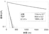
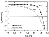
本発明者らは、不動態化剤、例えばハロゲン結合ドナー(例えばヨードペンタフルオロベンゼン)及び硫黄原子を含む有機分子(例えばチオフェン)を超分子集合体中に用いることによる、金属ハロゲン化物ペロブスカイトデバイスのための不動態化方法を導入した。窒素原子を含む不動態化剤(例えばピリジン)は、超分子集合体中の不動態化剤として使用することもできる。処理された太陽電池のPCEは、いくつかの百分率点の増加(例えば、13%から16%超)を示すことができ、増強の原因となる機序が解明された。処理を用いないと、配位不飽和なハロゲン化物アニオン及び欠陥部位は正孔-トラップとして作用し、ペロブスカイト/正孔輸送体ヘテロ接合での及びペロブスカイト内での電荷の著しい蓄積に至る。これは、より速い再結合に至り、正孔輸送体及びペロブスカイト膜内に不利な電荷密度プロファイルをもたらす可能性があり、これは、作業環境下での速い及び効果的な電荷抽出を阻害するはずである。該不動態化剤は、配位不飽和なハロゲン化物イオン及び欠陥部位からの静電気帯電に結合及びそれを遮蔽することができて、該課題を解決する。現在の技術を発展させることを超えて、この作業は、ペロブスカイト結晶の化学的処理が太陽電池における動作の増強に至り得ることを実証している。任意の配位不飽和なカチオン(Aイオン、Bイオン及びXイオン)及び欠陥部位を、大気酸素及び水に頼ることなく緩和することによって、性能及び再現性の両方におけるさらなる改善が予想される。加えて、該不動態化剤は、スズ及びゲルマニウム系のペロブスカイトなど、空気中で典型的に不安定であるペロブスカイトを安定化及び保護することができる。 The present inventors have investigated the use of passivating agents such as halogen bond donors (e.g. iodopentafluorobenzene) and organic molecules containing sulfur atoms (e.g. thiophene) in supramolecular assemblies for the preparation of metal halide perovskite devices. A passivation method for Passivating agents containing nitrogen atoms (eg pyridine) can also be used as passivating agents in supramolecular assemblies. The PCE of treated solar cells can show some percentage point increase (eg 13% to over 16%) and the mechanism responsible for the enhancement was elucidated. Without treatment, the coordinatively unsaturated halide anions and defect sites act as hole-traps leading to significant accumulation of charge at and within the perovskite/hole transporter heterojunction. This can lead to faster recombination and result in a disadvantageous charge density profile within the hole transporter and perovskite films, which should prevent fast and effective charge extraction in the work environment. Is. The passivating agent solves the problem by being able to bind to and shield electrostatic charges from coordination unsaturated halide ions and defect sites. Beyond developing current technology, this work demonstrates that chemical treatment of perovskite crystals can lead to enhanced operation in solar cells. By relaxing any coordinatively unsaturated cations (A, B and X ions) and defect sites without resorting to atmospheric oxygen and water, further improvements in both performance and reproducibility are expected. In addition, the passivating agent can stabilize and protect perovskites that are typically unstable in air, such as tin and germanium based perovskites.
したがって、本発明者らは、有機不動態化剤で不動態化されたペロブスカイトを含む効果的なデバイスを開発した。第1の態様によると、本発明は、
(a)金属ハロゲン化物ペロブスカイト、及び
(b)有機化合物である不動態化剤
を含む半導体であって、不動態化剤の分子が金属ハロゲン化物ペロブスカイト中のアニオン又はカチオンに化学的に結合している半導体を含むデバイスを提供する。該デバイスは、光電子デバイス、例えば光起電力デバイスであってよい。
Therefore, the inventors have developed an effective device containing perovskites passivated with an organic passivating agent. According to a first aspect, the invention provides
(a) metal halide perovskite, and
(b) A device comprising a semiconductor containing a passivating agent which is an organic compound, wherein the molecule of the passivating agent is chemically bonded to an anion or a cation in the metal halide perovskite. The device may be an optoelectronic device, such as a photovoltaic device.
本発明は、一般に、結晶性イオン性固体にも適用することができる。したがって、本発明は、
(a)結晶性イオン性固体、及び
(b)有機化合物である不動態化剤、
含む半導体であって、不動態化剤の分子が結晶性イオン性固体中のアニオン又はカチオンに化学的に結合している半導体を含むデバイスも提供する。該デバイスは、光電子デバイス、例えば光起電力デバイスであってよい。
The present invention is also generally applicable to crystalline ionic solids. Therefore, the present invention
(a) crystalline ionic solid, and
(b) a passivating agent which is an organic compound,
Also provided is a semiconductor-containing device comprising a semiconductor, wherein the passivating agent molecule is chemically bound to an anion or cation in the crystalline ionic solid. The device may be an optoelectronic device, such as a photovoltaic device.
本発明は、
(a)金属ハロゲン化物ペロブスカイト、及び
(b)
(i)ハロゲン結合ドナー化合物、又は
(ii)少なくとも1個のチオール基若しくはスルフィド基を含む有機化合物
である不動態化剤
を含む半導体を含むデバイスも提供する。該デバイスは、光電子デバイス、例えば光起電力デバイスであってよい。
The present invention is
(a) metal halide perovskite, and
(b)
(i) a halogen bond donor compound, or
(ii) Also provided is a device including a semiconductor containing a passivating agent which is an organic compound containing at least one thiol group or sulfide group. The device may be an optoelectronic device, such as a photovoltaic device.
本発明は、
(a)金属ハロゲン化物ペロブスカイト、及び
(b)有機化合物である不動態化剤
含む半導体であって、不動態化剤の分子が金属ハロゲン化物ペロブスカイト中のアニオン又はカチオンに化学的に結合している半導体を含むデバイスを製造するための方法も提供し、
ここで、該方法は、有機化合物であるとともに金属ハロゲン化物ペロブスカイト中のアニオン又はカチオンに化学的に結合するのに適当である不動態化剤で金属ハロゲン化物ペロブスカイトを処理することを含む。
The present invention is
(a) metal halide perovskite, and
(b) a semiconductor containing a passivating agent which is an organic compound, for producing a device comprising a semiconductor in which a molecule of the passivating agent is chemically bound to an anion or a cation in a metal halide perovskite Also provides a method,
Here, the method comprises treating the metal halide perovskite with a passivating agent that is an organic compound and is suitable for chemically bonding to anions or cations in the metal halide perovskite.
本発明は、
(a)結晶性イオン性固体、及び
(b)有機化合物である不動態化剤
を含む半導体であって、不動態化剤の分子が結晶性イオン性固体中のアニオン又はカチオンに化学的に結合している半導体を含むデバイスを製造するための方法も提供し、
ここで、該方法は、有機化合物であるとともに結晶性イオン性固体中のアニオン又はカチオンに化学的に結合するのに適当である不動態化剤で結晶性イオン性固体を処理することを含む。
The present invention is
(a) crystalline ionic solid, and
(b) A semiconductor containing a passivating agent that is an organic compound, wherein the molecule of the passivating agent is chemically bonded to an anion or a cation in a crystalline ionic solid is manufactured. Also provides a way to
Here, the method comprises treating the crystalline ionic solid with a passivating agent that is an organic compound and is suitable for chemically bonding to anions or cations in the crystalline ionic solid.
製造されるデバイスは、光電子デバイス、例えば光起電力デバイスであってよい。 The manufactured device may be an optoelectronic device, for example a photovoltaic device.
本発明は、本発明によるデバイスを製造するための方法によって得られるデバイスも提供する。該デバイスは、光電子デバイス、例えば光起電力デバイスであってよい。 The invention also provides a device obtained by the method for manufacturing a device according to the invention. The device may be an optoelectronic device, such as a photovoltaic device.
加えて、第2の態様によると、本発明は、
(a)金属ハロゲン化物ペロブスカイト、及び
(b)有機化合物である不動態化剤
含む半導体であって、不動態化剤の分子が金属ハロゲン化物ペロブスカイト内の粒界に配置されているとともに金属ハロゲン化物ペロブスカイト中のアニオン又はカチオンに化学的に結合されていない半導体を含むデバイスを提供する。該デバイスは、光電子デバイス、例えば光起電力デバイスであってよい。
In addition, according to a second aspect, the invention provides
(a) metal halide perovskite, and
(b) A semiconductor containing a passivating agent which is an organic compound, wherein the passivating agent molecule is arranged at a grain boundary in the metal halide perovskite and is chemically reacted with an anion or a cation in the metal halide perovskite. A device is provided that includes a semiconductor that is not bonded to. The device may be an optoelectronic device, such as a photovoltaic device.
そのため、本発明は、
(a)金属ハロゲン化物ペロブスカイト、及び
(b)非極性有機分子を含む有機化合物である不動態化剤
を含む半導体を含むデバイスも提供する。該デバイスは、光電子デバイス、例えば光起電力デバイスであってよい。
Therefore, the present invention is
(a) metal halide perovskite, and
(b) Also provided are devices that include a semiconductor that includes a passivating agent that is an organic compound that includes a non-polar organic molecule. The device may be an optoelectronic device, such as a photovoltaic device.
本発明は、
(a)金属ハロゲン化物ペロブスカイト、及び
(b)有機化合物である不動態化剤
含む半導体であって、不動態化剤の分子が金属ハロゲン化物ペロブスカイト内の粒界に配置されているとともに金属ハロゲン化物ペロブスカイト中のアニオン又はカチオンに化学的に結合されていない半導体を含むデバイスを製造するための方法も提供し、
ここで、該方法は、金属ハロゲン化物ペロブスカイト中のアニオン又はカチオンに化学的に結合しない有機化合物である不動態化剤で金属ハロゲン化物ペロブスカイトを処理することを含む。
The present invention is
(a) metal halide perovskite, and
(b) A semiconductor containing a passivating agent which is an organic compound, wherein the passivating agent molecule is arranged at a grain boundary in the metal halide perovskite and is chemically reacted with an anion or a cation in the metal halide perovskite. Also provided is a method for manufacturing a device that includes a semiconductor that is not bonded to
Here, the method comprises treating the metal halide perovskite with a passivating agent that is an organic compound that does not chemically bind to anions or cations in the metal halide perovskite.
製造されるデバイスは、光電子デバイス、例えば光起電力デバイスであってよい。 The manufactured device may be an optoelectronic device, for example a photovoltaic device.
本発明は、本発明によるデバイスを製造するための方法によって得られるデバイスも提供する。該デバイスは、光電子デバイス、例えば光起電力デバイスであってよい。 The invention also provides a device obtained by the method for manufacturing a device according to the invention. The device may be an optoelectronic device, such as a photovoltaic device.
定義
「ペロブスカイト」という用語は、本明細書で使用される場合、CaTiO3の構造に関連した三次元結晶構造を有する材料又はCaTiO3の構造に関連した構造を有する材料層を含む材料を指す。CaTiO3の構造は式ABX3によって表すことができ、式中A及びBは異なるサイズのカチオンであり、Xはアニオンである。単位格子において、Aカチオンは(0,0,0)であり、Bカチオは(1/2、1/2、1/2)であり、Xアニオンは(1/2、1/2、0)である。Aカチオンは通常Bカチオンよりも大きい。当業者は、A、B及びXを変動させる場合、異なるイオンサイズが、CaTiO3によって採用される構造からより低い対称性歪み構造にペロブスカイト材料の構造を歪ませる原因となり得ることを理解されよう。材料がCaTiO3の構造に関連した構造を有する層を含むならば、対称性も、より低い。ペロブスカイト材料の層を含む材料はよく知られている。例えば、K2NiF4型構造を採用する材料の構造は、ペロブスカイト材料の層を含む。当業者は、ペロブスカイト材料が、[A]が少なくとも1つのカチオンであり、[B]が少なくとも1つのカチオンであり、[X]が少なくとも1つのアニオンである式[A][B][X]3によって表すことができることを理解されよう。ペロブスカイトが1つを超えるAカチオンを含む場合、異なるAカチオンは、規則化又は不規則化されたやり方でA部位上に分布され得る。ペロブスカイトが1つを超えるBカチオンを含む場合、異なるBカチオンは、規則化又は不規則化されたやり方でB部位上に分布され得る。ペロブスカイトが1つを超えるXアニオンを含む場合、異なるXアニオンは、規則化又は不規則化されたやり方でX部位上に分布され得る。1つを超えるAカチオン、1つを超えるBカチオン又は1つを超えるXカチオンを含むペロブスカイトの対称性は、CaTiO3の対称性よりも低い。
Definitions The term "perovskite" as used herein, refers to a material comprising a material layer having a structure related to the structure of the material or CaTiO 3 having a three-dimensional crystal structure related to the structure of CaTiO 3. The structure of CaTiO 3 can be represented by the formula ABX 3 , where A and B are different size cations and X is an anion. In the unit cell, the A cation is (0,0,0), the B cation is (1/2, 1/2, 1/2) and the X anion is (1/2, 1/2, 0). Is. A cations are usually larger than B cations. Those skilled in the art will appreciate that when varying A, B and X, different ionic sizes may cause the structure of the perovskite material to distort from the structure employed by CaTiO 3 to a lower symmetrical strain structure. The symmetry is also lower if the material comprises a layer with a structure related to that of CaTiO 3 . Materials containing layers of perovskite materials are well known. For example, a material structure that employs a K 2 NiF 4 type structure includes a layer of perovskite material. Those skilled in the art will appreciate that the perovskite material has the formula [A][B][X] where [A] is at least one cation, [B] is at least one cation, and [X] is at least one anion. It will be appreciated that it can be represented by 3 . If the perovskite contains more than one A cation, the different A cations can be distributed on the A sites in an ordered or disordered manner. If the perovskite contains more than one B cation, the different B cations can be distributed on the B sites in an ordered or disordered manner. If the perovskite contains more than one X anion, the different X anions can be distributed on the X sites in an ordered or disordered manner. The symmetry of perovskites containing more than one A cation, more than one B cation or more than one X cation is less than that of CaTiO 3 .
「金属ハロゲン化物ペロブスカイト」という用語は、本明細書で使用される場合、式が少なくとも1つの金属カチオン及び少なくとも1つのハロゲン化物アニオンを含有するペロブスカイトを指す。「有機金属ハロゲン化物ペロブスカイト」という用語は、本明細書で使用される場合、その式が少なくとも1つの有機カチオンを含有する金属ハロゲン化物ペロブスカイトを指す。 The term "metal halide perovskite" as used herein refers to a perovskite whose formula contains at least one metal cation and at least one halide anion. The term "organometal halide perovskite" as used herein refers to a metal halide perovskite whose formula contains at least one organic cation.
「結晶性イオン性固体」という用語は、本明細書で使用される場合、アニオン及びカチオンを含む結晶構造を含む固体、例えば金属ハロゲン化物ペロブスカイト及び有機金属ハロゲン化物ペロブスカイトを指す。アニオン又はカチオンは、任意のアニオン又はカチオンであってよい。当業者が理解する通り、結晶構造は、ある程度の共有結合を有することができるが、しかしながら、「結晶性イオン性固体」という用語は、また、ある程度の共有結合を有する結晶性化合物を包含する。したがって、二酸化チタン及びヨウ化銅(I)などの化合物は、「結晶性イオン性固体」という用語内に入る。 The term "crystalline ionic solid", as used herein, refers to solids containing a crystalline structure containing anions and cations, such as metal halide perovskites and organometallic halide perovskites. The anion or cation can be any anion or cation. As one of ordinary skill in the art will appreciate, a crystal structure may have some degree of covalent bonding, however, the term "crystalline ionic solid" also includes crystalline compounds having some degree of covalent bonding. Thus, compounds such as titanium dioxide and copper(I) iodide fall within the term "crystalline ionic solid".
「化学結合」という用語は、本明細書で使用される場合、2個の原子間又はイオン間(原子-原子、原子-イオン及びイオン-イオン相互作用を含める)の誘引相互作用を指す。これは、特定の軌道相互作用であり得る。「化学結合」には超分子化学結合が含まれる。「超分子化学結合」という用語は、本明細書で使用される場合、化学結合における1個の原子又はイオンが1個の分子中にあるとともに他の原子又はイオンが別の分子中若しくは結晶構造中にある又は単離された原子又はイオンである化学結合を意味する。超分子結合は典型的に非共有結合である。 The term “chemical bond”, as used herein, refers to an attractive interaction between two atoms or ions (including atom-atom, atom-ion and ion-ion interactions). This can be a specific orbital interaction. "Chemical bond" includes supramolecular chemical bonds. The term "supramolecular chemical bond", as used herein, has one atom or ion in a chemical bond in one molecule and another atom or ion in another molecule or crystal structure. By a chemical bond that is an atom or ion that is in or isolated. Supramolecular bonds are typically non-covalent.
「化学的に結合している」という用語は、本明細書で使用される場合、化学結合が間にある分子、原子又はイオンから選択される2つの種を指し、超分子化学結合によって結合している分子、原子又はイオンから選択される2つの種への言及が含まれる。 The term "chemically bound", as used herein, refers to two species selected from molecules, atoms or ions with which the chemical bond is in-between and which are joined by a supramolecular chemical bond. Included is a reference to two species selected from a molecule, an atom or an ion.
「ハロゲン結合」という用語は、本明細書で使用される場合、ハロゲン原子とルイス塩基との間に形成される非共有結合性超分子化学結合を指す。ハロゲン結合において、ハロゲン原子は、求核性ルイス塩基と相互作用する求電子性種として作用する。有機分子中のハロゲン原子は、分子中の他の部分の電子求引効果により、又は誘起双極子の形成により、電子欠損性であり得る。アニオンなどのルイス塩基(ハロゲン化物アニオン、特にヨウ化物を含める)は、この特定の超分子相互作用を介してハロゲン化有機化合物と強く相互作用することができる。この相互作用は、求電子試薬としてハロゲン原子に関与する任意の超分子非共有結合を定義する。報告されている最も強いハロゲン結合ドナーの1つは、ヨードペンタフルオロベンゼンである(IPFB、図1c)。この化合物において、高電気陰性フッ素原子は芳香族環から電子密度を誘発的に引き出し、これは順じて、芳香族環に結合しているヨウ素から電子密度を引き出して、このハロゲン上に部分正電荷を残す。さらに、IPFBにおけるヨウ素上の電荷密度は、異方的に分布され、正静電位が、C-I結合軸の延長上の炭素の反対側に局在化される。この電気陽性領域は、任意の電子豊富部位(例えばルイス塩基)と誘引的に相互作用することができ、他のハロゲンアニオン(X-、ルイス塩基、図1c)との相互作用が殊に強い。ヨウ素上のこの陽性領域は負静電位のベルトによって囲まれているので、-C-I…X-の同軸配列からの任意のシフト(図1cを参照されたい)は静電反発をもたらす。したがって、角度-C-I…X-は常に180°に近いが、I…X-距離は特定の結晶性構造に依存する。 The term "halogen bond", as used herein, refers to a non-covalent, supramolecular chemical bond formed between a halogen atom and a Lewis base. In the halogen bond, the halogen atom acts as an electrophilic species that interacts with the nucleophilic Lewis base. Halogen atoms in organic molecules can be electron deficient due to electron-withdrawing effects of other moieties in the molecule or due to the formation of induced dipoles. Lewis bases such as anions (including halide anions, especially iodides) can interact strongly with halogenated organic compounds via this particular supramolecular interaction. This interaction defines any supramolecular non-covalent bond involving a halogen atom as an electrophile. One of the strongest halogen-bond donors reported is iodopentafluorobenzene (IPFB, Figure 1c). In this compound, the highly electronegative fluorine atom induces an electron density from the aromatic ring, which in turn draws an electron density from the iodine bound to the aromatic ring, resulting in a partial positive concentration on this halogen. Leave a charge. Furthermore, the charge density on iodine in IPFB is anisotropically distributed, with the positive electrostatic potential being localized on the opposite side of the carbon on the extension of the CI bond axis. This electropositive region is capable of attractively interacting with any electron-rich site (eg Lewis base) and is particularly strong with other halogen anions (X − , Lewis base, FIG. 1c). This positive areas of iodine Motojo is surrounded by a belt of a negative electrostatic potential, -CI ... X - (see Figure 1c) any shift from the coaxial arrangement of leads to electrostatic repulsion. Therefore, the angle -CI ... X - but close always 180 °, I ... X - distance will depend on the particular crystalline structure.
「ハロゲン結合ドナー化合物」という用語は、本明細書で使用される場合、ルイス塩基と相互作用することでハロゲン結合を形成する求電子性ハロゲン原子を含む化合物を指す。 The term "halogen bond donor compound" as used herein refers to a compound containing an electrophilic halogen atom that interacts with a Lewis base to form a halogen bond.
「カルコゲン」という用語は、本明細書で使用される場合、元素周期表の第16族から選択される元素を指す。したがって、カルコゲンには、O、S、Se及びTeが含まれる。時折、カルコゲンにはOが含まれるとは受け止められない。したがって、カルコゲンにはS、Se及びTeが含まれると理解され得る。
The term "chalcogen", as used herein, refers to an element selected from
「カルコゲン-金属結合」という用語は、本明細書で使用される場合、カルコゲン原子又はアニオンと金属原子又はカチオンとの間に形成される化学結合を指す。これには、酸素原子と金属カチオン若しくは原子との間又は硫黄原子と金属カチオン若しくは原子との間の化学結合が含まれる。カルコゲン-金属結合は、しばしば、金属原子又はカチオンがルイス酸として作用し、カルコゲン原子又はアニオンがルイス塩基として作用する供与共有結合である。硫黄は強い硫黄-金属結合を形成することができる。 The term "chalcogen-metal bond", as used herein, refers to a chemical bond formed between a chalcogen atom or anion and a metal atom or cation. This includes chemical bonds between oxygen atoms and metal cations or atoms or between sulfur atoms and metal cations or atoms. Chalcogen-metal bonds are often covalent donor bonds in which the metal atom or cation acts as a Lewis acid and the chalcogen atom or anion acts as a Lewis base. Sulfur can form strong sulfur-metal bonds.
「配位不飽和な」という用語は、本明細書で使用される場合、配位が結晶の残り(又はバルク)における同じ型の他のイオンより低い結晶構造におけるアニオン又はカチオンを指す。例えば、結晶のバルクにおけるカチオンが6つの最近接のアニオンによって配位されているならば、5つ以下の最近接のアニオンによって配位されている同じ結晶構造におけるカチオンは、したがって、配位不飽和である。配位不飽和なイオンは、表面にイオンを配位させるための表面を超えて存在する結晶のさらなる単位格子がないことにより、結晶の表面に発生し得るか、又は配位不飽和なイオンは、結晶のバルクにおいて、結晶欠陥(即ち欠陥部位)、例えば空孔(即ち、特に1対のイオンが存在しない場合の、時々ショットキー欠陥として知られているイオンの非存在)がある部位に発生することがあり、したがって、空孔に隣接するイオンは、1つの最近接の対イオンを欠如する。 The term "coordinatively unsaturated" as used herein refers to an anion or cation in the crystal structure whose coordination is lower than other ions of the same type in the rest (or bulk) of the crystal. For example, if the cations in the bulk of the crystal are coordinated by the 6 closest anions, then the cations in the same crystal structure coordinated by the 5 or less closest anions will therefore be coordinated unsaturated. Is. Coordinatively unsaturated ions can occur on the surface of the crystal due to the absence of additional unit cells of the crystal that are present beyond the surface to coordinate the ions to the surface, or , In the bulk of the crystal, where there are crystal defects (ie defect sites), eg vacancies (ie the absence of ions, sometimes known as Schottky defects, especially when there is no pair of ions present) Therefore, the ion adjacent to the vacancy lacks one closest counterion.
「欠陥部位」という用語は、本明細書で使用される場合、局所的結晶構造がバルク材料の結晶構造に対応しない結晶格子における欠陥を指す。欠陥部位には、点欠陥、線欠陥及び平面欠陥が含まれる。点欠陥としては、空孔欠陥(イオンの非存在)、格子間欠陥(追加イオンの格子間含有)、フレンケル欠陥(格子間欠陥及び空孔欠陥からなる、近接に位置する1対の欠陥)及び不純物イオンの存在が挙げられる。平面欠陥としては、粒界及び積層欠陥が挙げられる。 The term "defect site", as used herein, refers to a defect in the crystal lattice whose local crystal structure does not correspond to that of the bulk material. The defect portion includes a point defect, a line defect and a plane defect. As point defects, vacancy defects (absence of ions), interstitial defects (interstitial inclusion of additional ions), Frenkel defects (a pair of defects located close to each other, consisting of interstitial defects and vacancy defects) and The presence of impurity ions may be mentioned. Plane defects include grain boundaries and stacking faults.
「粒界」という用語は、本明細書で使用される場合、結晶性固体内の異なる結晶配向の領域(即ち、結晶粒)を分離させる平面欠陥を指す。そのため粒界は、結晶性物質における2つの隣接する粒子間又は結晶子間の界面である。粒界欠陥は、材料の電気伝導率及び熱伝導率を減少することがあり、その上、腐食の開始には好ましい部位である。 The term “grain boundary”, as used herein, refers to a planar defect that separates regions of different crystalline orientation (ie, grains) within a crystalline solid. As such, grain boundaries are interfaces between two adjacent grains or crystallites in a crystalline material. Grain boundary defects can reduce the electrical and thermal conductivity of the material and are, in addition, a preferred site for initiation of corrosion.
「有機化合物」という用語は、当技術分野におけるそれの通常の意味を取る。典型的に、有機化合物は炭素原子を含む。当業者がそれを理解する通り、有機化合物は、別の炭素原子に、又は水素原子に、又はハロゲン原子に、又はカルコゲン原子(例えば、酸素原子、硫黄原子、セレン原子又はテルル原子)に共有結合している炭素原子を含むことができる。したがって、「有機化合物」という用語には、テトラヨードメタン及びヨードペンタフルオロベンゼンなどの過ハロゲン化有機化合物などの化合物、並びにシュウ酸、尿素及びチオ尿素などの化合物が含まれる。当業者は、「有機化合物」という用語には典型的に、例えば炭化物など、優勢にイオン性である化合物が含まれないことを理解されよう。 The term "organic compound" takes its ordinary meaning in the art. Typically, the organic compound contains carbon atoms. As one of ordinary skill in the art will appreciate, an organic compound is covalently bonded to another carbon atom, or to a hydrogen atom, or to a halogen atom, or to a chalcogen atom (e.g., oxygen atom, sulfur atom, selenium atom, or tellurium atom). Can include a carbon atom. Thus, the term "organic compound" includes compounds such as perhalogenated organic compounds such as tetraiodomethane and iodopentafluorobenzene, as well as compounds such as oxalic acid, urea and thiourea. Those skilled in the art will understand that the term "organic compound" typically does not include compounds that are predominantly ionic, such as, for example, carbides.
「チオール基」という用語は、本明細書で使用される場合、-SH基を指す。「スルフィド基」という用語は、本明細書で使用される場合、-S-基、即ち、2個の他の基に結合している硫黄原子を指し、ここで典型的に、硫黄原子は2個の炭素原子に結合している。 The term “thiol group” as used herein refers to a —SH group. The term “sulfide group” as used herein refers to a —S— group, ie, a sulfur atom attached to two other groups, where typically the sulfur atom is 2 Bound to carbon atoms.
「電子求引基」という用語は、本明細書で使用される場合、電子を、それが付着されている部分から引き出す基を指す。電子求引基は、しばしば、ハロゲン原子、カルボニル基及びニトロ基などの電気陰性基を含有する。 The term “electron-withdrawing group” as used herein refers to a group that withdraws an electron from the moiety to which it is attached. Electron-withdrawing groups often contain electronegative groups such as halogen atoms, carbonyl groups and nitro groups.
「アルキル」という用語は、本明細書で使用される場合、直鎖状又は分岐鎖の飽和炭化水素基を指す。アルキル基は、C1〜18アルキル基、C1〜14アルキル基、C1〜10アルキル基、C1〜6アルキル基又はC1〜4アルキル基であってよい。C1〜10アルキル基の例は、メチル、エチル、プロピル、ブチル、ペンチル、ヘキシル、ヘプチル、オクチル、ノニル又はデシルである。C1〜6アルキル基の例は、メチル、エチル、プロピル、ブチル、ペンチル又はヘキシルである。C1〜4アルキル基の例は、メチル、エチル、i-プロピル、n-プロピル、t-ブチル、s-ブチル又はn-ブチルである。「アルキル」という用語が本明細書のどこかで炭素の数を特定する接頭辞なしに使用されるならば、それは1個から6個の炭素を有する(そしてこれは、本明細書において言及される任意の他の有機基にも当てはまる)。 The term "alkyl", as used herein, refers to a straight or branched chain saturated hydrocarbon group. The alkyl group may be a C 1-18 alkyl group, a C 1-14 alkyl group, a C 1-10 alkyl group, a C 1-6 alkyl group or a C 1-4 alkyl group. Examples of C 1-10 alkyl groups are methyl, ethyl, propyl, butyl, pentyl, hexyl, heptyl, octyl, nonyl or decyl. Examples of C 1-6 alkyl groups are methyl, ethyl, propyl, butyl, pentyl or hexyl. Examples of C 1-4 alkyl groups are methyl, ethyl, i-propyl, n-propyl, t-butyl, s-butyl or n-butyl. If the term "alkyl" is used anywhere in the specification without a prefix specifying the number of carbons, it has 1 to 6 carbons (and this is referred to herein). The same applies to any other organic group).
「シクロアルキル」という用語は、本明細書で使用される場合、飽和また部分的不飽和の環式炭化水素基を指す。シクロアルキル基は、C3〜10シクロアルキル基、C3〜8シクロアルキル基又はC3〜6シクロアルキル基であってよい。C3〜8シクロアルキル基の例としては、シクロプロピル、シクロブチル、シクロペンチル、シクロヘキシル、シクロヘキセニル、シクロヘキサ-1,3-ジエニル、シクロヘプチル及びシクロオクチルが挙げられる。C3〜6シクロアルキル基の例としては、シクロプロピル、シクロブチル、シクロペンチル、及びシクロヘキシルが挙げられる。 The term "cycloalkyl" as used herein refers to a saturated or partially unsaturated cyclic hydrocarbon group. The cycloalkyl group may be a C3-10 cycloalkyl group, a C3-8 cycloalkyl group or a C3-6 cycloalkyl group. Examples of C3-8 cycloalkyl groups include cyclopropyl, cyclobutyl, cyclopentyl, cyclohexyl, cyclohexenyl, cyclohexa-1,3-dienyl, cycloheptyl and cyclooctyl. Examples of C3-6 cycloalkyl groups include cyclopropyl, cyclobutyl, cyclopentyl, and cyclohexyl.
「アルケニル」という用語は、本明細書で使用される場合、1個以上の二重結合を含む直鎖状又は分岐鎖の炭化水素基を指す。アルケニル基は、C2〜18アルケニル基、C2〜14アルケニル基、C2〜10アルケニル基、C2〜6アルケニル基又はC2〜4アルケニル基であってよい。C2〜10アルケニル基の例は、エテニル(ビニル)、プロペニル、ブテニル、ペンテニル、ヘキセニル、ヘプテニル、オクテニル、ノネニル又はデセニルである。C2〜6アルケニル基の例は、エテニル、プロペニル、ブテニル、ペンテニル又はヘキセニルである。C2〜4アルケニル基の例は、エテニル、i-プロペニル、n-プロペニル、s-ブテニル又はn-ブテニルである。アルケニル基は典型的に1個又は2個の二重結合を含む。 The term "alkenyl" as used herein refers to a straight or branched chain hydrocarbon group containing one or more double bonds. The alkenyl group may be a C 2-18 alkenyl group, a C 2-14 alkenyl group, a C 2-10 alkenyl group, a C 2-6 alkenyl group or a C 2-4 alkenyl group. Examples of C 2-10 alkenyl groups are ethenyl (vinyl), propenyl, butenyl, pentenyl, hexenyl, heptenyl, octenyl, nonenyl or decenyl. Examples of C 2 to 6 alkenyl groups are ethenyl, propenyl, butenyl, pentenyl or hexenyl. Examples of C2-4 alkenyl groups are ethenyl, i-propenyl, n-propenyl, s-butenyl or n-butenyl. An alkenyl group typically contains one or two double bonds.
「アルキニル」という用語は、本明細書で使用される場合、1個以上の三重結合を含む直鎖状又は分岐鎖の炭化水素基を指す。アルキニル基は、C2〜18アルキニル基、C2〜14アルキニル基、C2〜10アルキニル基、C2〜6アルキニル基又はC2〜4アルキニル基であってよい。C2〜10アルキニル基の例は、エチニル、プロピニル、ブチニル、ペンチニル、ヘキシニル、ヘプチニル、オクチニル、ノニニル又はデシニルである。C1〜6アルキニル基の例は、エチニル、プロピニル、ブチニル、ペンチニル又はヘキシニルである。アルキニル基は典型的に1個又は2個の三重結合を含む。 The term "alkynyl" as used herein refers to a straight or branched chain hydrocarbon group containing one or more triple bonds. The alkynyl group may be a C 2-18 alkynyl group, a C 2-14 alkynyl group, a C 2-10 alkynyl group, a C 2-6 alkynyl group or a C 2-4 alkynyl group. Examples of C 2-10 alkynyl groups are ethynyl, propynyl, butynyl, pentynyl, hexynyl, heptynyl, octynyl, nonynyl or decynyl. Examples of C 1-6 alkynyl groups are ethynyl, propynyl, butynyl, pentynyl or hexynyl. An alkynyl group typically contains one or two triple bonds.
「アリール」という用語は、本明細書で使用される場合、環部分に6個から14個の炭素原子、典型的には6個から10個の炭素原子を含有する単環式、二環式又は多環式の芳香族環を指す。例としては、フェニル基、ナフチル基、インデニル基及びインダニル基が挙げられる。「アリール基」という用語には、本明細書で使用される場合、ヘテロアリール基が含まれる。「ヘテロアリール」という用語は、本明細書で使用される場合、1個以上のヘテロ原子を含めて、環部分に6個から10個の原子を典型的に含有する単環式又は二環式のヘテロ芳香族環を指す。ヘテロアリール基は、一般に、O、S、N、P、Se及びSiから選択される少なくとも1個のヘテロ原子を含有する5員又は6員の環である。それは、例えば、1個、2個又は3個のヘテロ原子を含有する。ヘテロアリール基の例としては、ピリジル、ピラジニル、ピリミジニル、ピリダジニル、フラニル、チエニル、ピラゾリジニル、ピロリル、オキサゾリル、オキサジアゾリル、イソオキサゾリル、チアジアゾリル、チアゾリル、イソチアゾリル、イミダゾリル、ピラゾリル、キノリル及びイソキノリルが挙げられる。 The term "aryl", as used herein, is a monocyclic, bicyclic ring containing 6 to 14 carbon atoms in the ring portion, typically 6 to 10 carbon atoms. Alternatively, it refers to a polycyclic aromatic ring. Examples include phenyl, naphthyl, indenyl and indanyl groups. The term "aryl group", as used herein, includes heteroaryl groups. The term "heteroaryl," as used herein, includes one or more heteroatoms, and is typically monocyclic or bicyclic, containing from 6 to 10 atoms in the ring portion. Refers to the heteroaromatic ring of. Heteroaryl groups are generally 5- or 6-membered rings containing at least one heteroatom selected from O, S, N, P, Se and Si. It contains, for example, 1, 2 or 3 heteroatoms. Examples of heteroaryl groups include pyridyl, pyrazinyl, pyrimidinyl, pyridazinyl, furanyl, thienyl, pyrazolidinyl, pyrrolyl, oxazolyl, oxadiazolyl, isoxazolyl, thiadiazolyl, thiazolyl, isothiazolyl, imidazolyl, pyrazolyl, quinolyl and isoquinolyl.
「アルキレン」、「シクロアルキレン」、「アルケニレン」、「アルキニレン」及び「アリーレン」という用語は、本明細書で使用される場合、アルキル基、シクロアルキル基、アルケニル基、アルキニル基又はアリール基からそれぞれ水素原子を除去することによって得られる二価の基を指す。アルキレン基は、C1〜18アルキレン基、C1〜14アルキレン基、C1〜10アルキレン基、C1〜6アルキレン基又はC1〜4アルキレン基であってよい。C1〜6アルキレン基の例は、メチレン、エチレン、プロピレン、ブチレン、ペンチレン及びヘキシレンである。シクロアルキレン基は、C3〜10シクロアルキレン基、C3〜8シクロアルキレン基又はC3〜6シクロアルキレン基であってよい。C3〜6シクロアルキレン基の例としては、シクロペンチレン及びシクロヘキシレンが挙げられる。アルケニレン基は、C2〜18アルケニレン基、C2〜14アルケニレン基、C2〜10アルケニレン基、C2〜6アルケニレン基又はC2〜4アルケニレン基であってよい。C2〜4アルケニレン基の例としては、エテニレン(ビニレン)、プロペニレン及びブテニレンが挙げられる。アルキニレン基は、C2〜18アルキニレン基、C2〜14アルキニレン基、C2〜10アルキニレン基、C2〜6アルキニレン基又はC2〜4アルキニレン基であってよい。C2〜4アルキニレン基の例としては、エチニレン及びプロピニレンが挙げられる。アリーレン基の例としては、フェニレン及びチオフェンから誘導されるジラジカルが挙げられる。アルキレン、シクロアルキレン、アルケニレン、アルキニレン、及びアリーレンに関して、これらの基は、他の基に、該基上の任意の2つの位置で結合されていてよい。したがって、プロピレンとしては、-CH2CH2CH2-及び-CH2CH(CH3)-が挙げられ、フェニレンとしては、オルト-、メタ-及びパラ-フェニレンが挙げられる。 The terms "alkylene", "cycloalkylene", "alkenylene", "alkynylene" and "arylene", as used herein, are each an alkyl group, cycloalkyl group, alkenyl group, alkynyl group or aryl group. A divalent group obtained by removing a hydrogen atom. The alkylene group may be a C 1-18 alkylene group, a C 1-14 alkylene group, a C 1-10 alkylene group, a C 1-6 alkylene group or a C 1-4 alkylene group. Examples of C1-6 alkylene groups are methylene, ethylene, propylene, butylene, pentylene and hexylene. The cycloalkylene group may be a C3-10 cycloalkylene group, a C3-8 cycloalkylene group or a C3-6 cycloalkylene group. Examples of C3-6 cycloalkylene groups include cyclopentylene and cyclohexylene. The alkenylene group may be a C 2-18 alkenylene group, a C 2-14 alkenylene group, a C 2-10 alkenylene group, a C 2-6 alkenylene group or a C 2-4 alkenylene group. Examples of C 2-4 alkenylene groups include ethenylene (vinylene), propenylene and butenylene. The alkynylene group may be a C 2-18 alkynylene group, a C 2-14 alkynylene group, a C 2-10 alkynylene group, a C 2-6 alkynylene group or a C 2-4 alkynylene group. Examples of C2-4 alkynylene groups include ethynylene and propynylene. Examples of arylene groups include diradicals derived from phenylene and thiophene. For alkylene, cycloalkylene, alkenylene, alkynylene, and arylene, these groups may be attached to the other groups at any two positions on the group. Accordingly, the propylene, -CH 2 CH 2 CH 2 - and -CH 2 CH (CH 3) -. Examples of the phenylene, ortho -, meta - and para - include phenylene.
「置換されている」という用語は、置換されている有機基の文脈において本明細書で使用される場合、C1〜10アルキル、アリール(本明細書において定義されている通り)、シアノ、アミノ、ニトロ、C1〜10アルキルアミノ、ジ(C1-10)アルキルアミノ、アリールアミノ、ジアリールアミノ、アリール(C1-10)アルキルアミノ、アミド、アシルアミド、ヒドロキシ、オキソ、ハロ、カルボキシ、エステル、アシル、アシルオキシ、C1〜10アルコキシ、アリールオキシ、ハロ(C1-10)アルキル、スルホン酸、チオール、C1〜10アルキルチオ、アリールチオ、スルホニル、リン酸、リン酸エステル、ホスホン酸及びホスホン酸エステルから選択される1個以上の置換基を持つ有機基を指す。置換アルキル基の例としては、ハロアルキル基、ペルハロアルキル基、ヒドロキシアルキル基、アミノアルキル基、アルコキシアルキル基及びアルカリール基が挙げられる。基が置換されている場合、それは1個、2個又は3個の置換基を持つ。例えば、置換されている基は、1個又は2個の置換基を有することができる。 The term "substituted," as used herein in the context of a substituted organic group, is C 1-10 alkyl, aryl (as defined herein), cyano, amino. , Nitro, C 1-10 alkylamino, di(C 1-10 )alkylamino, arylamino, diarylamino, aryl(C 1-10 )alkylamino, amide, acylamide, hydroxy, oxo, halo, carboxy, ester, Acyl, acyloxy, C 1-10 alkoxy, aryloxy, halo(C 1-10 )alkyl, sulfonic acid, thiol, C 1-10 alkylthio, arylthio, sulfonyl, phosphoric acid, phosphoric acid ester, phosphonic acid and phosphonic acid ester Refers to an organic group having one or more substituents selected from Examples of the substituted alkyl group include a haloalkyl group, a perhaloalkyl group, a hydroxyalkyl group, an aminoalkyl group, an alkoxyalkyl group and an alkaryl group. When a group is substituted it has 1, 2 or 3 substituents. For example, a substituted group can have 1 or 2 substituents.
「ペルハロアルキル」という用語は、本明細書で使用される場合、全て又はほぼ全てのH原子がハロゲン原子で置き換えられているアルキル基を指す。典型的に、5個のうち3個の水素原子がハロゲン原子で置き換えられている。したがって、ペルハロアルキル基としては、例えば、-(CF2)3F、-(CCl2)2(CF2)2H、及び-(CHCl)(CF2)Hが挙げられる。 The term "perhaloalkyl", as used herein, refers to an alkyl group in which all or nearly all H atoms have been replaced with halogen atoms. Typically, 3 out of 5 hydrogen atoms are replaced by halogen atoms. Therefore, the perhaloalkyl group, for example, - (CF 2) 3 F , - (CCl 2) 2 (CF 2) 2 H, and - (CHCl) (CF 2) H and the like.
「オリゴマー」という用語は、本明細書で使用される場合、少数の反復単位(即ち、少数のモノマー)を含む分子を指す。典型的に、オリゴマーは、2個から9個のモノマー又は3個から6個のモノマーを含む。 The term "oligomer" as used herein refers to a molecule that contains a small number of repeating units (ie, a small number of monomers). Typically, the oligomer comprises 2 to 9 monomers or 3 to 6 monomers.
「バンドギャップ」という用語は、本明細書で使用される場合、材料における原子価バンドの上部と伝導バンドの底部との間のエネルギー差異を指す。当業者は、過度の実験を要することなく材料のバンドギャップを容易に測定することができる。 The term "bandgap" as used herein refers to the energy difference between the top of the valence band and the bottom of the conduction band in a material. Those skilled in the art can easily measure the band gap of a material without undue experimentation.
「層」という用語は、本明細書で使用される場合、形態が実質的に層状である(例えば、2つの垂直方向に実質的に延長するが、第3の垂直方向におけるそれの延長が制限される)任意の構造を指す。層は、層の範囲にわたって変動する厚さを有し得る。典型的に、層は、およそ一定の厚さを有する。層の「厚さ」は、本明細書で使用される場合、層の平均厚さを指す。層の厚さは、例えば、膜の横断面の電子顕微鏡法などの顕微鏡法を使用することによって、又は例えば触針形状測定器を使用する表面形状測定によって、簡便に測定することができる。 The term "layer", as used herein, is substantially layered in form (e.g., substantially extending in two vertical directions, but limited in its extension in a third vertical direction). ) Refers to any structure. The layers can have a thickness that varies over the extent of the layers. Typically the layers have an approximately constant thickness. “Thickness” of a layer, as used herein, refers to the average thickness of the layer. Layer thickness can be conveniently measured, for example, by using microscopy, such as electron microscopy of cross-sections of the membrane, or by profilometry, for example using a stylometer.
「多孔質」という用語は、本明細書で使用される場合、中に細孔が配列されている材料を指す。したがって、例えば、多孔質材料において、細孔は、材料がない足場内の体積である。材料における細孔としては、「閉鎖」細孔並びに開放細孔が挙げられ得る。閉鎖細孔は、非接続空洞、即ち、材料内で単離されているとともに任意の他の細孔に接続されておらず、そのため材料が曝露される流体によってアクセスされ得ない細孔である、材料中の細孔である。他方で、「開放細孔」は、こうした流体によってアクセス可能である。開放及び閉鎖の多孔性の概念は、J. Rouquerolら、「Recommendations for the Characterization of Porous Solids」、Pure & Appl. Chem.、66巻、8号、1739〜1758ページ、1994において詳細に考察されている。そのため、開放多孔性は、流体流が有効に行われる多孔質材料の合計体積の画分を指す。そのため、それは閉鎖細孔を除く。「開放多孔性」という用語は、「接続多孔性」及び「有効多孔性」という用語と相互交換可能であり、当技術分野において、共通して、単純に「多孔性」に縮められる。そのため「開放多孔性がない」という用語は、本明細書で使用される場合、有効多孔性がない材料を指す。「非多孔質」という用語は、本明細書で使用される場合、任意の多孔性がない、即ち、開放多孔性がない及びその上閉鎖多孔性がない材料を指す。 The term "porous", as used herein, refers to a material having pores arranged therein. Thus, for example, in a porous material, the pores are the volume within the material-free scaffold. The pores in the material can include "closed" pores as well as open pores. Closed pores are unconnected cavities, i.e. pores that are isolated in the material and are not connected to any other pores, so that the material cannot be accessed by the fluid to which it is exposed, The pores in the material. On the other hand, "open pores" are accessible by such fluids. The concept of open and closed porosity is discussed in detail in J. Rouquerol et al., "Recommendations for the Characterization of Porous Solids", Pure & Appl. Chem., 66, 8, 1739-1758, 1994. There is. As such, open porosity refers to the fraction of the total volume of porous material in which fluid flow is effectively performed. Therefore, it excludes closed pores. The term "open porosity" is interchangeable with the terms "connected porosity" and "effective porosity" and is commonly referred to in the art as simply "porous". As such, the term "no open porosity" as used herein refers to a material that has no effective porosity. The term “non-porous”, as used herein, refers to a material that is free of any porosity, ie, open porosity and as well as closed porosity.
「半導体」という用語は、本明細書で使用される場合、導体及び誘電体の電気伝導率間の大きさが中間の電気伝導率を有する材料を指す。半導体は、n型半導体、p型半導体又は真性半導体であってよい。 The term "semiconductor" as used herein refers to a material having an electrical conductivity that is intermediate in magnitude between the electrical conductivity of a conductor and a dielectric. The semiconductor may be an n-type semiconductor, a p-type semiconductor or an intrinsic semiconductor.
「n型領域」という用語は、本明細書で使用される場合、1種以上の電子輸送(即ち、n型)材料の領域を指す。同様に、「n型層」という用語は、電子輸送(即ち、n型)材料の層を指す。電子輸送(即ちn型)材料は、単一の電子輸送化合物若しくは元素材料、又は2種以上の電子輸送化合物若しくは元素材料の混合物であってよい。電子輸送化合物又は元素材料は非ドープであるか、又は1種以上のドーパント元素でドープすることができる。 The term "n-type region," as used herein, refers to a region of one or more electron-transporting (ie, n-type) materials. Similarly, the term “n-type layer” refers to a layer of electron-transporting (ie, n-type) material. The electron-transporting (ie, n-type) material can be a single electron-transporting compound or elemental material, or a mixture of two or more electron-transporting compounds or elemental materials. The electron transport compound or elemental material can be undoped or doped with one or more dopant elements.
「p型領域」という用語は、本明細書で使用される場合、1つ以上の正孔輸送(即ち、p型)材料の領域を指す。同様に、「p型層」という用語は、正孔輸送(即ち、p型)材料の層を指す。正孔輸送(即ち、p型)材料は、単一の正孔輸送化合物若しくは元素材料、又は2種以上の正孔輸送化合物若しくは元素材料の混合物であってよい。正孔輸送化合物又は元素材料は非ドープであるか、又は1種以上のドーパント元素でドープすることができる。 The term “p-type region” as used herein refers to a region of one or more hole-transporting (ie p-type) materials. Similarly, the term "p-type layer" refers to a layer of hole-transporting (ie, p-type) material. The hole-transporting (ie, p-type) material can be a single hole-transporting compound or elemental material, or a mixture of two or more hole-transporting compounds or elemental materials. The hole-transporting compound or elemental material can be undoped or doped with one or more dopant elements.
「処理すること」という用語は、本明細書で使用される場合、1つの化合物が別の化合物と反応又は相互作用するようにされる任意のプロセスを指す。他方の化合物を処理する一方の化合物は、それ自体化合物として添加することができるか、又は一部のプロセスによってそれ自体化合物に変換する前駆体として添加することができる。 The term "treating" as used herein refers to any process by which one compound is made to react or interact with another compound. Treating the other compound One compound can be added as a compound itself, or as a precursor that is converted into a compound itself by some process.
「上に配置する」という用語は、本明細書で使用される場合、1つの構成成分を利用可能にすること又は別の構成成分の上に置くことを指す。第1の構成成分は、利用可能にする若しくは第2の構成成分上に直接置くことができるか、又は第1の構成成分と第2の構成成分との間に介在する第3の構成成分があってよい。例えば、第1の層が第2の層上に配置されるならば、これとしては、第1の層と第2の層との間に介在する第3の層がある場合が挙げられる。しかしながら、典型的に、「上に配置する」は、1つの構成成分を別の構成成分上に直接置くことを指す。 The term "disposed on," as used herein, refers to making one component available or putting it on top of another. The first component can be made available or placed directly on the second component, or a third component intervening between the first and second components is You can For example, if the first layer is disposed on the second layer, this would include the case where there is a third layer interposed between the first and second layers. However, typically, “disposed on” refers to placing one component directly on another.
「電極材料」という用語は、本明細書で使用される場合、電極における使用に適当な任意の材料を指す。電極材料は高い電気伝導率を有する。 The term "electrode material" as used herein refers to any material suitable for use in electrodes. The electrode material has a high electrical conductivity.
デバイス
第1の態様において、本発明は、
(a)金属ハロゲン化物ペロブスカイト、及び
(b)有機化合物である不動態化剤、
含む半導体であって、不動態化剤の分子が金属ハロゲン化物ペロブスカイト中のアニオン又はカチオンに化学的に結合している半導体を含むデバイスを提供する。金属ハロゲン化物ペロブスカイトは、有機金属ハロゲン化物ペロブスカイトであってよい。
Device In a first aspect, the invention provides
(a) metal halide perovskite, and
(b) a passivating agent which is an organic compound,
There is provided a device comprising a semiconductor comprising a molecule of a passivating agent chemically bound to an anion or cation in a metal halide perovskite. The metal halide perovskite may be an organometallic halide perovskite.
通常、本発明の第1の実施形態のデバイス及び方法における半導体は、(a)前記金属ハロゲン化物ペロブスカイトを(b)不動態化剤に加えて含み、本発明は、一般に、それらの用語で後述される。しかしながら、上に記述されている通り、本発明は、金属ハロゲン化物ペロブスカイト半導体だけでなく、金属ハロゲン化物ペロブスカイト以外の結晶性イオン性固体半導体、例えば金属酸化物半導体などを含めて、一般に、結晶性イオン性固体半導体にも適用可能である。金属酸化物半導体は、それ自体よく知られており、チタニアは、こうした金属酸化物半導体の1つの例である。したがって、当業者が理解する通り、金属ハロゲン化物ペロブスカイトの点から後述されている本発明の実施形態のいずれも、任意のイオン結晶性固体、例えば金属酸化物、例えばチタニアなどを使用して実施することもできる。通常、結晶性イオン性固体は、例えば、本明細書においてさらに記載又は定義されている金属ハロゲン化物ペロブスカイトのいずれかであってよい金属ハロゲン化物ペロブスカイトである。しかしながら、代替として、結晶性イオン性固体は、異なる結晶性イオン性固体、例えば金属酸化物を含むことができる。しばしば用いられる1種の金属酸化物は、二酸化チタンである。 Generally, the semiconductor in the device and method of the first embodiment of the invention comprises (a) the metal halide perovskite in addition to (b) a passivating agent, the present invention generally being described in those terms below. To be done. However, as described above, the present invention generally relates to crystalline crystalline ionic solid state semiconductors other than metal halide perovskite semiconductors, such as metal oxide semiconductors, such as metal oxide semiconductors. It is also applicable to ionic solid semiconductors. Metal oxide semiconductors are well known per se, and titania is one example of such a metal oxide semiconductor. Thus, as those skilled in the art will appreciate, any of the embodiments of the invention described below in terms of metal halide perovskites are carried out using any ionic crystalline solid such as a metal oxide such as titania. You can also Generally, the crystalline ionic solid is a metal halide perovskite, which can be, for example, any of the metal halide perovskites described or defined further herein. However, as an alternative, the crystalline ionic solid may comprise a different crystalline ionic solid, eg a metal oxide. One metal oxide that is often used is titanium dioxide.
したがって、別の態様において、本発明の第1の態様は、(a)結晶性イオン性固体及び(b)有機化合物である不動態化剤を含む半導体であって、不動態化剤の分子が結晶性イオン性固体中のアニオン又はカチオンに化学的に結合している半導体を含むデバイスを提供する。 Therefore, in another aspect, the first aspect of the present invention is a semiconductor comprising a passivating agent which is (a) a crystalline ionic solid and (b) an organic compound, wherein the molecule of the passivating agent is Provided is a device comprising a semiconductor chemically bound to an anion or cation in a crystalline ionic solid.
デバイスが結晶性イオン性固体を含む場合、結晶性イオン性固体は、本明細書のどこかで定義されている任意のイオン性固体を含むことができる。例えば、結晶性イオン性固体は、本明細書に記載されている通りの無機n型材料又は無機p型材料、特に結晶性の無機n型材料を含むことができる。したがって、結晶性イオン性固体は、金属酸化物を含むことができる。デバイスは、(a)金属酸化物及び(b)有機化合物である不動態化剤を含む半導体であって、不動態化剤の分子が金属酸化物中のアニオン又はカチオンに化学的に結合している半導体を含むことができる。金属酸化物は、しばしば、チタン、スズ、亜鉛、ニオブ、タンタル、タングステン、インジウム、ガリウム、ネオジム、パラジウム若しくはカドミウムの酸化物、又は前記金属の2種以上の混合物の酸化物である。例えば、イオン性固体は、TiO2、SnO2、ZnO、Nb2O5、Ta2O5、WO3、W2O5、In2O3、Ga2O3、Nd2O3、PbO及びCdOから選択される金属酸化物であってよい。特に、金属酸化物はTiO2であってよい。結晶性イオン性固体は、本明細書に記載されているもののいずれかなどの無機p型材料を含むことができる。結晶性イオン性固体は、半導性金属ハロゲン化物、又は銅を含む半導性化合物を含むことができる。例えば、結晶性イオン性固体は、CuI、CuBr、CuSCN、Cu2O、CuO又はCISを含むことができる。
Where the device comprises a crystalline ionic solid, the crystalline ionic solid can include any ionic solid defined elsewhere herein. For example, the crystalline ionic solid can include an inorganic n-type material or an inorganic p-type material as described herein, especially a crystalline inorganic n-type material. Therefore, the crystalline ionic solid can include a metal oxide. The device is a semiconductor containing a passivating agent which is (a) a metal oxide and (b) an organic compound, wherein a molecule of the passivating agent is chemically bonded to an anion or a cation in the metal oxide. Can include semiconductors. The metal oxide is often an oxide of titanium, tin, zinc, niobium, tantalum, tungsten, indium, gallium, neodymium, palladium or cadmium, or an oxide of a mixture of two or more of the above metals. For example, ionic solids, TiO 2, SnO 2, ZnO , Nb 2
第1の態様において、不動態化剤は有機化合物である。不動態化剤は、2000gmol-1以下又は1000gmol-1以下の分子量を有する有機化合物であってよい。不動態化剤は、1個以上のヘテロ原子を含む有機化合物であってよい。不動態化剤は、典型的に、1個から10個のヘテロ原子を含む又は1個から6個のヘテロ原子を含む有機化合物である。ヘテロ原子は、通常、周期表のp-ブロック(Cを除く)から選択される。例えば、1個以上のヘテロ原子は、独立して、N、P、As、O、S、Se、Te、F、Cl、Br及びIから選択することができる。通常、1個以上のヘテロ原子は、各々独立して、N、P、O、S、Se、Te、F、Cl、Br及びIから選択される。典型的に、1個以上の又は1個から6個のヘテロ原子は、N、O、S、Se、Te、F、Cl、Br及びI、例えばO、S、F、Cl、Br及びI、又はN、S、F、Cl、Br及びIから各々独立して選択されるヘテロ原子であってよい。不動態化剤は、典型的に、O、S、F、Cl、Br及びIから選択される1個以上の原子を含む有機化合物である。不動態化剤は、S、F、Cl、Br及びIから選択される1個以上の原子を含む有機化合物であってよい。有機化合物は、ヘテロ原子の1つ以上の異なる型を含むことができる。 In the first embodiment, the passivating agent is an organic compound. The passivating agent may be an organic compound having a molecular weight of 2000 gmol -1 or less or 1000 gmol -1 or less. The passivating agent may be an organic compound containing one or more heteroatoms. The passivating agent is typically an organic compound containing from 1 to 10 heteroatoms or from 1 to 6 heteroatoms. Heteroatoms are usually selected from the p-blocks of the Periodic Table (excluding C). For example, the one or more heteroatoms can be independently selected from N, P, As, O, S, Se, Te, F, Cl, Br and I. Usually, the one or more heteroatoms are each independently selected from N, P, O, S, Se, Te, F, Cl, Br and I. Typically, one or more or 1 to 6 heteroatoms are N, O, S, Se, Te, F, Cl, Br and I, such as O, S, F, Cl, Br and I, Alternatively, it may be a heteroatom independently selected from N, S, F, Cl, Br and I. The passivating agent is typically an organic compound containing one or more atoms selected from O, S, F, Cl, Br and I. The passivating agent may be an organic compound containing one or more atoms selected from S, F, Cl, Br and I. Organic compounds can include one or more different types of heteroatoms.
第1の態様において、不動態化剤は、N、P、S、F、Cl、Br及びIから選択される1個以上の原子を含む有機化合物であってよい。不動態化剤は、N、P及びSから選択される1個以上の原子を含む有機化合物であってよい。一実施形態において、不動態化剤は、N及びPから選択される1個以上の原子を含む有機化合物である。 In the first aspect, the passivating agent may be an organic compound containing one or more atoms selected from N, P, S, F, Cl, Br and I. The passivating agent may be an organic compound containing one or more atoms selected from N, P and S. In one embodiment, the passivating agent is an organic compound containing one or more atoms selected from N and P.
第1の態様において、不動態化剤の分子の少なくとも一部は、金属ハロゲン化物ペロブスカイト中のアニオン又はカチオンに化学的に結合している。典型的に、不動態化剤の分子は、超分子化学結合によって金属ハロゲン化物ペロブスカイト中のアニオン又はカチオンに化学的に結合している。不動態化剤の分子の全て又は基本的に全ては、金属ハロゲン化物ペロブスカイト中のアニオン又はカチオンに結合することができる。不動態化剤の分子の50%以上又は70%以上は、典型的に、金属ハロゲン化物ペロブスカイト中のアニオン又はカチオンに結合している。例えば、不動態化剤の分子の90%以上は、典型的に、金属ハロゲン化物ペロブスカイト中のアニオン又はカチオンに結合している。不動態化剤の分子は、しばしば、不動態化剤の分子中のヘテロ原子を介して金属ハロゲン化物ペロブスカイト中のアニオン又はカチオンに結合している。「結合している(bonded)」という言葉は、「結合されている(bound)」と相互交換可能に使用することができる。 In the first embodiment, at least a portion of the passivating agent molecule is chemically bound to an anion or cation in the metal halide perovskite. Typically, the passivator molecule is chemically bound to an anion or cation in the metal halide perovskite by a supramolecular chemical bond. All or essentially all of the passivating agent molecules can bind to anions or cations in the metal halide perovskite. More than 50% or more than 70% of the molecules of the passivator are typically bound to anions or cations in the metal halide perovskite. For example, 90% or more of the molecules of the passivating agent are typically bound to anions or cations in the metal halide perovskite. The passivator molecule is often attached to an anion or cation in the metal halide perovskite via a heteroatom in the passivator molecule. The term "bonded" may be used interchangeably with "bound."
化学結合は典型的に超分子化学結合である。したがって、半導体は、(a)金属ハロゲン化物ペロブスカイト及び(b)有機化合物である不動態化剤を含むことができ、ここで、不動態化剤の分子は、金属ハロゲン化物ペロブスカイト中のアニオン又はカチオンに超分子的に化学的に結合している。 The chemical bond is typically a supramolecular chemical bond. Thus, the semiconductor may include a passivating agent that is (a) a metal halide perovskite and (b) an organic compound, where the passivating agent molecule is an anion or a cation in the metal halide perovskite. Is chemically bound supramolecularly.
不動態化剤の分子と金属ハロゲン化物ペロブスカイト中のアニオン又はカチオンとの間の化学結合は、通常、ハロゲン結合及びカルコゲン-金属結合から選択される。カルコゲン-金属結合は、酸素-金属結合、硫黄-金属結合、又はセレン-金属結合から選択することができる。典型的に、カルコゲン-金属結合は硫黄-金属結合である。カルコゲン-金属結合は供与共有結合であり得る。 The chemical bond between the molecule of the passivator and the anion or cation in the metal halide perovskite is usually selected from halogen bonds and chalcogen-metal bonds. The chalcogen-metal bond can be selected from an oxygen-metal bond, a sulfur-metal bond, or a selenium-metal bond. Typically the chalcogen-metal bond is a sulfur-metal bond. The chalcogen-metal bond can be a covalent donor bond.
不動態化剤の分子と金属ハロゲン化物ペロブスカイト中のアニオン又はカチオンとの間の化学結合は、代替として、窒素-金属結合及びリン-金属結合から選択することができる。窒素-金属結合において、不動態化剤中の窒素原子は、孤立電子対を介して金属イオン又は原子に配位することができる。窒素-金属結合は供与共有結合であってよい。リン-金属結合において、不動態化剤中のリン原子は、孤立電子対を介して金属イオン又は原子に配位することができる。リン-金属結合は供与共有結合であってよい。窒素-金属結合及びリン金属結合の両方が典型的に超分子結合である。 The chemical bond between the molecule of the passivating agent and the anion or cation in the metal halide perovskite can alternatively be selected from nitrogen-metal bonds and phosphorus-metal bonds. In the nitrogen-metal bond, the nitrogen atom in the passivating agent can coordinate to the metal ion or atom via the lone pair of electrons. The nitrogen-metal bond may be a covalent donor bond. In a phosphorus-metal bond, the phosphorus atom in the passivating agent can coordinate to the metal ion or atom via the lone pair of electrons. The phosphorus-metal bond may be a covalent donor bond. Both nitrogen-metal and phosphorus metal bonds are typically supramolecular bonds.
不動態化剤の分子が結合している金属ハロゲン化物ペロブスカイト中のカチオン又はアニオンは、典型的に配位不飽和である。配位不飽和なアニオン及びカチオンは、ペロブスカイトの曝露表面に位置されていてよいか、又は欠陥部位若しくはその近くのペロブスカイトのバルクにあってよい。配位不飽和なアニオン又はカチオンは、1つ、2つ、3つ又は4つの最近接の対イオンの非存在により、配位不飽和とすることができる。 The cation or anion in the metal halide perovskite to which the passivator molecule is attached is typically coordinately unsaturated. Coordinatively unsaturated anions and cations may be located on the exposed surface of the perovskite, or may be in the bulk of the perovskite at or near the defect site. The coordinatively unsaturated anion or cation can be coordinatively unsaturated due to the absence of one, two, three or four closest counterions.
不動態化剤の分子が結合している金属ハロゲン化物ペロブスカイト中のアニオン又はカチオンの少なくとも一部は、金属ハロゲン化物ペロブスカイトの表面に、又は金属ハロゲン化物ペロブスカイトの結晶構造のバルク中の欠陥部位にあってよい。しばしば、不動態化剤の分子が結合している金属ハロゲン化物ペロブスカイト中のアニオン又はカチオンは、金属ハロゲン化物ペロブスカイトの表面に、及び金属ハロゲン化物ペロブスカイトのバルク中の粒界にあってよい。 At least some of the anions or cations in the metal halide perovskite to which the passivator molecule is attached are located at the surface of the metal halide perovskite or at defect sites in the bulk of the metal halide perovskite crystal structure. You can Often, the anion or cation in the metal halide perovskite to which the passivator molecule is attached may be at the surface of the metal halide perovskite and at grain boundaries in the bulk of the metal halide perovskite.
第2の態様において、本発明は、
(a)金属ハロゲン化物ペロブスカイト、及び
(b)有機化合物である不動態化剤、
を含む半導体であって、不動態化剤の分子が金属ハロゲン化物ペロブスカイト内の粒界に配置されているとともに金属ハロゲン化物ペロブスカイト中のアニオン又はカチオンに化学的に結合されていない半導体を含むデバイスを提供する。金属ハロゲン化物ペロブスカイトは、有機金属ハロゲン化物ペロブスカイトであってよい。該デバイスは、光電子デバイス、例えば光起電力デバイスであってよい。
In a second aspect, the invention provides
(a) metal halide perovskite, and
(b) a passivating agent which is an organic compound,
And a device containing a semiconductor in which the passivator molecule is located at a grain boundary in the metal halide perovskite and is not chemically bound to an anion or a cation in the metal halide perovskite. provide. The metal halide perovskite may be an organometallic halide perovskite. The device may be an optoelectronic device, such as a photovoltaic device.
そのため、本発明の第2の態様は、(a)結晶性イオン性固体及び(b)有機化合物である不動態化剤を含む半導体であって、不動態化剤の分子が結晶性イオン性固体内の粒界に配置されているとともに結晶性イオン性固体中のアニオン又はカチオンに化学的に結合されていない半導体を含むデバイスも提供する。 Therefore, the second aspect of the present invention is a semiconductor containing a passivating agent which is (a) a crystalline ionic solid and (b) an organic compound, wherein the molecule of the passivating agent is a crystalline ionic solid. Also provided is a device that includes a semiconductor disposed at a grain boundary within and not chemically bound to an anion or cation in a crystalline ionic solid.
第2の態様において、不動態化剤は、非極性有機分子を含む有機化合物であってよい。不動態化剤は、多環式芳香族炭化水素分子を含む有機化合物であってよい。 In the second aspect, the passivating agent may be an organic compound comprising a non-polar organic molecule. The passivating agent may be an organic compound containing polycyclic aromatic hydrocarbon molecules.
不動態化剤及び不動態化
上に記載されている通り、第1の態様において、有機化合物である不動態化剤は、典型的に、1個以上のヘテロ原子を含む有機化合物である。不動態化剤は、孤立電子対を有するヘテロ原子を含む有機化合物であってよい。孤立電子対は、金属ハロゲン化物ペロブスカイト中のイオンと相互作用することで、化学結合、例えば配位結合などの超分子結合を形成することができる。
Passivating Agents and Passivation As described above, in the first embodiment, the passivating agent, which is an organic compound, is typically an organic compound containing one or more heteroatoms. The passivating agent may be an organic compound containing a heteroatom with a lone pair of electrons. The lone pair of electrons can form a chemical bond, for example, a supramolecular bond such as a coordinate bond, by interacting with an ion in the metal halide perovskite.
典型的に、金属ハロゲン化物ペロブスカイトの式は、化合物A又は化合物のカチオンAH+を含有し、不動態化剤は化合物Aでない。したがって、金属ハロゲン化物ペロブスカイトの式に特定のアルキルアンモニウムイオンが含まれるならば、第1の態様の不動態化剤は、対応するアルキルアミンでない。 Typically, the metal halide perovskite formula contains compound A or the cation AH + of the compound and the passivating agent is not compound A. Thus, if the formula for the metal halide perovskite includes a particular alkylammonium ion, the passivating agent of the first aspect is not the corresponding alkylamine.
第1の態様において、不動態化剤は、(a)ハロゲン結合ドナー化合物及び(b)孤立電子対を有する少なくとも1個のヘテロ原子を含む有機化合物から選択される化合物であってよい。孤立電子対を有する少なくとも1個のヘテロ原子を含む有機化合物は、N、P、As、O、S、Se及びTeから選択される少なくとも1個のヘテロ原子を含む有機化合物から選択することができる。孤立電子対を有する少なくとも1個のヘテロ原子を含む有機化合物は、典型的に、N、P、O、S及びSeから選択される又はN、O及びSから選択される少なくとも1つのヘテロ原子を含む有機化合物から選択される。不動態化剤は、(a)ハロゲン結合ドナー化合物及び(b)N、P、As、O、S、Se及びTeから選択される少なくとも1個のヘテロ原子を含む有機化合物から選択される化合物であってよい。不動態化剤は、(a)ハロゲン結合ドナー化合物、及び(b)N、P、O、S及びSe、又はN、O及びSから選択される少なくとも1個のヘテロ原子を含む有機化合物から選択される化合物であってよい。 In the first aspect, the passivating agent may be a compound selected from (a) a halogen bond donor compound and (b) an organic compound containing at least one heteroatom having a lone pair of electrons. The organic compound containing at least one heteroatom having a lone pair of electrons can be selected from organic compounds containing at least one heteroatom selected from N, P, As, O, S, Se and Te. .. Organic compounds containing at least one heteroatom having a lone pair of electrons typically contain at least one heteroatom selected from N, P, O, S and Se, or N, O and S. Selected from organic compounds including. The passivating agent is a compound selected from (a) a halogen bond donor compound and (b) an organic compound containing at least one heteroatom selected from N, P, As, O, S, Se and Te. You can The passivating agent is selected from (a) a halogen-bond donor compound, and (b) an organic compound containing at least one heteroatom selected from N, P, O, S and Se, or N, O and S. The compound may be
少なくとも1つのNを含む化合物の例としては、アミン、イミン、ニトリル、ヒドラジン、ピリジン、2H-ピロール、ピロール、2-ピロリン、3-ピロリン、ピロリジン、オキサゾール、チアゾール、イミダゾール、2-イミダゾリン、イミダゾリジン、ピラゾール、2-ピラゾリン、及び他の窒素含有ヘテロ環から選択される基を含む化合物が挙げられる。例えば、少なくとも1つのNを含む化合物は、アミン、イミン、ニトリル、ヒドラジン、ピリジン及びピロリジンから選択される基を含む化合物であってよい。したがって、不動態化剤は、置換若しくは非置換アミン、置換若しくは非置換イミン、置換若しくは非置換ピリジン又は置換若しくは非置換ピロリジンであってよい。 Examples of compounds containing at least one N include amine, imine, nitrile, hydrazine, pyridine, 2H-pyrrole, pyrrole, 2-pyrroline, 3-pyrroline, pyrrolidine, oxazole, thiazole, imidazole, 2-imidazoline, imidazolidine. , Pyrazole, 2-pyrazoline, and other nitrogen-containing heterocycles. For example, the compound containing at least one N may be a compound containing a group selected from amine, imine, nitrile, hydrazine, pyridine and pyrrolidine. Thus, the passivating agent may be a substituted or unsubstituted amine, a substituted or unsubstituted imine, a substituted or unsubstituted pyridine or a substituted or unsubstituted pyrrolidine.
本発明の第1の態様によるデバイスにおいて、不動態化剤は、(a)ハロゲン結合ドナー化合物及び(b)少なくとも1個のチオール基又はスルフィド基を含む有機化合物から選択される化合物であってよい。不動態化剤は、N及びPから選択される少なくとも1個のヘテロ原子を含む有機化合物であってよい。 In the device according to the first aspect of the present invention, the passivating agent may be a compound selected from (a) a halogen-bonded donor compound and (b) an organic compound containing at least one thiol group or sulfide group. .. The passivating agent may be an organic compound containing at least one heteroatom selected from N and P.
第1の態様の不動態化剤は、ハロゲン結合ドナー化合物であってよい。不動態化剤は、少なくとも1個のチオール基又はスルフィド基を含む有機化合物であってよい。デバイスは、さらなる不動態化剤を含むことができる。したがって、デバイスは、第2の不動態化剤をさらに含むことができる。例えば、デバイスは、ハロゲン結合ドナー化合物である第1の不動態化剤及び少なくとも1個のチオール基又はスルフィド基を含む有機化合物である第2の不動態化剤を含むことができる。 The passivating agent of the first aspect may be a halogen bond donor compound. The passivating agent may be an organic compound containing at least one thiol group or sulfide group. The device can include additional passivating agents. Thus, the device can further include a second passivating agent. For example, the device can include a first passivating agent that is a halogen-bonded donor compound and a second passivating agent that is an organic compound containing at least one thiol or sulfide group.
第1の態様の不動態化剤は、式X-EWGのハロゲン結合ドナー化合物であってよく、式中、Xは、I、Br、Cl及びFから選択されるハロゲンであり、EWGは、電子求引基である。EWGは、Xから電子を誘引的に又は共役的に引き出す任意の基であってよい。EWGは、炭素の電気陰性度よりも大きい電気陰性度を有する1個以上の原子を含む有機基であってよい。EWGは、2.6以上のポーリング電気陰性度を有する1個以上の、2個以上の、3個以上の又は3個から6個の原子を含むことができる。EWGは、2.9以上のポーリング電気陰性度を有する1個以上の、2個以上の、3個以上の又は3個から6個の原子を含むことができる。2.6以上又は2.9以上のポーリング電気陰性度を有する原子は、10個以下又は6個以下の結合によってXから分離することができる。ポーリング電気陰性度値の表は、当業者に利用可能である。ポーリング電気陰性度値としては、Fには2.98、Oには3.44、Clには3.16、Nには3.04、及びBrには2.96が挙げられる。EWGは、F、Cl、Br、I、O及びSから選択される2個以上の、3個以上の、4個以上の又は5個以上の原子を含む有機基であってよい。EWGはペルハロ-C1〜12-アルキル基であってよい。例えば、EWGは、トリフルオルメチル、ペンタフルオロエチル又はヘプタフルオロプロピル、ペルフルオロブチル、ペルフルオロペンチル、ペルフルオロヘキシル、ペルフルオロヘプチル、ペルフルオロオクチル、ペルフルオロノニル又はペルフルオロデシルなど、ペルフルオロ-C1〜12-アルキル基であってよい。 The passivating agent of the first aspect may be a halogen-bonded donor compound of formula X-EWG, where X is a halogen selected from I, Br, Cl and F and EWG is an electron. It is an attractive group. The EWG can be any group that attracts or conjugately withdraws an electron from X. The EWG may be an organic group containing one or more atoms with an electronegativity that is greater than the electronegativity of carbon. The EWG can include one or more, two or more, three or more, or three to six atoms with a Pauling electronegativity of 2.6 or more. The EWG can include one or more, two or more, three or more, or three to six atoms with a Pauling electronegativity of 2.9 or more. Atoms with a Pauling electronegativity of 2.6 or higher or 2.9 or higher can be separated from X by 10 or fewer or 6 or fewer bonds. A table of Pauling electronegativity values is available to one of ordinary skill in the art. Pauling electronegativity values include 2.98 for F, 3.44 for O, 3.16 for Cl, 3.04 for N, and 2.96 for Br. The EWG may be an organic group containing 2 or more, 3 or more, 4 or more or 5 or more atoms selected from F, Cl, Br, I, O and S. EWG may be a perhalo-C 1-12 -alkyl group. For example, EWG is a perfluoro-C 1-12 -alkyl group such as trifluoromethyl, pentafluoroethyl or heptafluoropropyl, perfluorobutyl, perfluoropentyl, perfluorohexyl, perfluoroheptyl, perfluorooctyl, perfluorononyl or perfluorodecyl. You may
Xは、I、Br、Cl及びFから、I、Br及びClから、又はI及びBrから選択することができる。例えば、XはIであってよい。 X can be selected from I, Br, Cl and F, from I, Br and Cl, or from I and Br. For example, X can be I.
第1の態様の不動態化剤は、しばしば、式X-EWGのハロゲン結合ドナー化合物であり、式中、
Xは、I、Br、Cl及びFから選択されるハロゲンであり、
EWGは、-(CY2)nY、-(CY2)nR、-(CR2)nY、-(CR2)nR、
-(CY2)nCR3、-(CR2)nCY3、-(CY2)n(CR2)mY、-(CR2)n(CY2)mY、-(CY2)n(CR2)mR、
-(CR2)n(CY2)mR、-(CY2)n(CR2)mCY3、-(CR2)n(CY2)mCR3、-(CRaYb)nY、-(CRaYb)nR、
-C6Y5、-(C6R)Y4、-(C6R2)Y3、-(C6R3)Y2、-(C6R4)Y、-CY=CYR、-CY=CR2、-CR=CYR、
-C≡CY、-C≡CR、-COR、-COCYR2及び-COCY2Rから選択される基であり、ここで、
各Yは同じ又は異なっており、I、Br、Cl及びFから選択されるハロゲンであり、
各Rは同じ又は異なっており、H、ヒドロキシ、ニトリル、ニトロ、非置換又は置換C1〜18-アルキル、非置換又は置換C3〜10-シクロアルキル、非置換又は置換C2〜18-アルケニル、非置換又は置換C2〜18-アルキニル、及び非置換又は置換アリールから選択される基であり、
nは、1から18の整数であり、
mは、1から18の整数であり、
各aは同じ又は異なっており、0、1又は2であり、
各bは同じ又は異なっており、0、1又は2であり、
各CRaYb基におけるa及びbの和は、2である。
The passivating agent of the first aspect is often a halogen-bond donor compound of formula X-EWG, wherein
X is a halogen selected from I, Br, Cl and F,
EWG is, - (CY 2) n Y , - (CY 2) n R, - (CR 2) n Y, - (CR 2) n R,
-(CY 2 ) n CR 3 , -(CR 2 ) n CY 3 , -(CY 2 ) n (CR 2 ) m Y, -(CR 2 ) n (CY 2 ) m Y, -(CY 2 ) n (CR 2 ) m R,
-(CR 2 ) n (CY 2 ) m R, -(CY 2 ) n (CR 2 ) m CY 3 , -(CR 2 ) n (CY 2 ) m CR 3 , -(CR a Y b ) n Y , -(CR a Y b ) n R,
-C 6 Y 5 , -(C 6 R)Y 4 , -(C 6 R 2 )Y 3 , -(C 6 R 3 )Y 2 , -(C 6 R 4 )Y, -CY=CYR,- CY=CR 2 , -CR=CYR,
A group selected from -C≡CY, -C≡CR, -COR, -COCYR 2 and -COCY 2 R, wherein:
Each Y is the same or different and is a halogen selected from I, Br, Cl and F,
Each R is the same or different and is H, hydroxy, nitrile, nitro, unsubstituted or substituted C 1-18 -alkyl, unsubstituted or substituted C 3-10 -cycloalkyl, unsubstituted or substituted C 2-18 -alkenyl. A group selected from unsubstituted or substituted C 2-18 -alkynyl, and unsubstituted or substituted aryl,
n is an integer from 1 to 18,
m is an integer from 1 to 18,
Each a is the same or different and is 0, 1 or 2,
Each b is the same or different and is 0, 1 or 2,
The sum of a and b in each CR a Y b group is 2.
したがって、-(CRaYb)nY基及び-(CRaYb)nR基としては、任意の数のハロゲン原子で置換されている任意の直鎖アルキル基が挙げられる。例えば、-(CRaYb)nYとしては、-(CClH)(CH2)2(CFI)Br及び-(CHF)3CF3が挙げられる。 Thus, the -(CR a Y b ) n Y group and the -(CR a Y b ) n R group include any linear alkyl group substituted with any number of halogen atoms. For example, - as a (CR a Y b) n Y , - (CClH) (CH 2) 2 (CFI) Br and - (CHF) 3 CF 3 and the like.
しばしば、nは1から6の整数であり、mは1から6の整数である。EWGは、-(CY2)nY、-(CY2)nR、-(CR2)nY、-(CR2)nR、-(CY2)nCR3、-(CR2)nCY3、-(CY2)n(CR2)mY、-(CR2)n(CY2)mY、-(CY2)n(CR2)mR、-(CR2)n(CY2)mR、-(CY2)n(CR2)mCY3、-(CR2)n(CY2)mCR3、-(CRaYb)nY、-(CRaYb)nR、-C6Y5、-(C6R)Y4、-(C6R2)Y3、-(C6R3)Y2、-(C6R4)Y、-CY=CYR、-CY=CR2、-CR=CYR、-C≡CY、-C≡CR、-COR、-COCYR2及び-COCY2Rから選択される基であってよく、ここで、各Yは同じ又は異なっており、I、Br、Cl及びFから選択されるハロゲンであり、各Rは同じ又は異なっており、H、ヒドロキシ、ニトリル、ニトロ、非置換又は置換C1〜18-アルキル、非置換又は置換C3〜10-シクロアルキル、非置換又は置換C2〜18-アルケニル、非置換又は置換C2〜18-アルキニル、及び非置換又は置換アリールから選択される基であり、nは1から6の整数であり、mは1から6の整数であり、各aは同じ又は異なっており、0、1又は2であり、各bは同じ又は異なっており、0、1又は2であり、各CRaYb基におけるa及びbの和は2である。しばしば、Rは非置換である。各Rは同じ又は異なっており、通常、H、ヒドロキシ、ニトリル、ニトロ、非置換C1〜10-アルキル、非置換C3〜10-シクロアルキル、非置換C2〜10-アルケニル、非置換C2〜10-アルキニル、及び非置換アリールから選択される基である。 Often, n is an integer from 1 to 6 and m is an integer from 1 to 6. EWG has -(CY 2 ) n Y, -(CY 2 ) n R, -(CR 2 ) n Y, -(CR 2 ) n R, -(CY 2 ) n CR 3 , -(CR 2 ) n CY 3 , -(CY 2 ) n (CR 2 ) m Y, -(CR 2 ) n (CY 2 ) m Y, -(CY 2 ) n (CR 2 ) m R, -(CR 2 ) n (CY 2 ) m R, -(CY 2 ) n (CR 2 ) m CY 3 , -(CR 2 ) n (CY 2 ) m CR 3 , -(CR a Y b ) n Y, -(CR a Y b ) n R, -C 6 Y 5 , -(C 6 R)Y 4 , -(C 6 R 2 )Y 3 , -(C 6 R 3 )Y 2 , -(C 6 R 4 )Y, -CY= It may be a group selected from CYR, -CY=CR 2 , -CR=CYR, -C≡CY, -C≡CR, -COR, -COCYR 2 and -COCY 2 R, wherein each Y is The same or different, a halogen selected from I, Br, Cl and F, each R being the same or different, H, hydroxy, nitrile, nitro, unsubstituted or substituted C 1-18 -alkyl, non- A group selected from substituted or substituted C3-10 -cycloalkyl, unsubstituted or substituted C2-18 -alkenyl, unsubstituted or substituted C2-18 -alkynyl, and unsubstituted or substituted aryl, n being 1 To 6 is an integer, m is an integer from 1 to 6, each a is the same or different, 0, 1 or 2, each b is the same or different, 0, 1 or 2. , The sum of a and b in each CR a Y b group is 2. Often R is unsubstituted. Each R is the same or different and is usually H, hydroxy, nitrile, nitro, unsubstituted C 1-10 -alkyl, unsubstituted C 3-10 -cycloalkyl, unsubstituted C 2-10 -alkenyl, unsubstituted C A group selected from 2-10 -alkynyl and unsubstituted aryl.
第1の態様の不動態化剤は、式X-EWGのハロゲン結合ドナー化合物であってよく、式中、Xは、I、Br、Cl及びFから選択されるハロゲンであり、EWGは、-CY3、-(CY2)2Y、-(CY2)3Y、-CY2R、-(CY2)2R、-(CY2)3R、-CR2Y、-C6Y5、-(C6R)Y4、-(C6R2)Y3、-(C6R3)Y2、-(C6R4)Y、-CY=CYR、-CY=CR2、-C≡CY、-COR、-COCYR2及び-COCY2Rから選択される基であり、ここで、各Yは同じ又は異なっており、I、Br、Cl及びFから選択されるハロゲンであり、各Rは同じ又は異なっており、H、ヒドロキシ、ニトリル、ニトロ、非置換又は置換C1〜18-アルキル、非置換又は置換C3〜10-シクロアルキル、非置換又は置換C2〜18-アルケニル、非置換又は置換C2〜18-アルキニル、及び非置換又は置換アリールから選択される基である。 The passivating agent of the first aspect may be a halogen-bonded donor compound of formula X-EWG, wherein X is a halogen selected from I, Br, Cl and F and EWG is: CY 3 , -(CY 2 ) 2 Y, -(CY 2 ) 3 Y, -CY 2 R, -(CY 2 ) 2 R, -(CY 2 ) 3 R, -CR 2 Y, -C 6 Y 5 , -(C 6 R)Y 4 , -(C 6 R 2 )Y 3 , -(C 6 R 3 )Y 2 , -(C 6 R 4 )Y, -CY=CYR, -CY=CR 2 , A group selected from -C≡CY, -COR, -COCYR 2 and -COCY 2 R, wherein each Y is the same or different and is a halogen selected from I, Br, Cl and F. , Each R is the same or different and is H, hydroxy, nitrile, nitro, unsubstituted or substituted C 1-18 -alkyl, unsubstituted or substituted C 3-10 -cycloalkyl, unsubstituted or substituted C 2-18- A group selected from alkenyl, unsubstituted or substituted C 2-18 -alkynyl, and unsubstituted or substituted aryl.
EWGは、-CY3、-(CY2)2Y、-(CY2)3Y、-(CY2)2R、-(CY2)3R、-C6Y5、-(C6R)Y4、-(C6R2)Y3、-COR、-COCYR2及び-COCY2Rから選択される基であってよい。Xは、I、Br及びClから選択することができる。Yは、I、Br、Cl及びFから、Br、Cl及びFから、又はCl及びFからから選択することができる。例えば、YはFであってよい。Xは、I及びBrから選択することができ、Yは、Cl及びFから選択することができる。 EWG is -CY 3 , -(CY 2 ) 2 Y, -(CY 2 ) 3 Y, -(CY 2 ) 2 R, -(CY 2 ) 3 R, -C 6 Y 5 , -(C 6 R )Y 4 , -(C 6 R 2 )Y 3 , -COR, -COCYR 2 and -COCY 2 R may be a group selected from these groups. X can be selected from I, Br and Cl. Y can be selected from I, Br, Cl and F, from Br, Cl and F, or from Cl and F. For example, Y may be F. X can be selected from I and Br and Y can be selected from Cl and F.
第1の態様の不動態化剤は、しばしば、X(CY2)mCY3及び
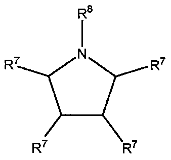
第1の態様の不動態化剤は、I(CY2)mCY3及び
第1の態様の不動態化剤は、I(CF2)mCF3及び
しばしば、mは0から8である。典型的に、nは2から5である。典型的に、Xは、I又はBrから選択され、Yは、Br、Cl及びFから選択することができる。 Often, m is 0-8. Typically n is 2 to 5. Typically X can be selected from I or Br and Y can be selected from Br, Cl and F.
第1の態様の不動態化剤は、例えば、ヨードペンタフルオロベンゼン、ヨードテトラフルオロベンゼン、ヨードクロロテトラフルオロベンゼン、ヨードジクロロトリフルオロベンゼン、ヨードクロロトリフルオロベンゼン、ヨードトリフルオロベンゼン、ヨードジクロロジフルオロベンゼン及びヨードジフルオロベンゼンから選択することができる。 The passivating agent of the first embodiment is, for example, iodopentafluorobenzene, iodotetrafluorobenzene, iodochlorotetrafluorobenzene, iododichlorotrifluorobenzene, iodochlorotrifluorobenzene, iodotrifluorobenzene, iododichlorodifluorobenzene. And iododifluorobenzene.
第1の態様の不動態化剤は、ヨードペンタフルオロベンゼン及びペルフルオロ-C1〜12アルキルヨウ素から選択することができる。しばしば、不動態化剤は、ヨードペンタフルオロベンゼン、ペルフルオロ-n-ブチルヨウ素、ペルフルオロ-n-ヘキシルヨウ素及びペルフルオロ-n-デシルヨウ素から選択される。ヨードペンタフルオロベンゼンは、式IC6F5を有する。 The passivating agent of the first aspect may be selected from iodopentafluorobenzene and perfluoro-C 1-12 alkyliodine . Often, the passivating agent is selected from iodopentafluorobenzene, perfluoro-n-butyl iodine, perfluoro-n-hexyl iodine and perfluoro-n-decyl iodine. Iodopentafluorobenzene has the formula IC 6 F 5 .
第1の態様の不動態化剤は、ペロブスカイト中の金属イオンとともにカルコゲン-金属結合を形成するのに適当である有機分子であってよい。したがって、不動態化剤は、カルコゲン原子を含む有機分子であり得る。不動態化剤は、1個以上の、例えば2個以上のカルコゲン原子を含む化合物であり得る。例えば、不動態化剤は、ヒドロキシ基を含む有機化合物、エーテル基を含む化合物、有機硫黄化合物、有機セレン化合物、又は有機テルル化合物であってよい。したがって、不動態化剤は、有機硫黄化合物又は有機セレン化合物であり得る。しばしば、不動態化剤は有機硫黄化合物である。 The passivating agent of the first aspect may be an organic molecule suitable for forming a chalcogen-metal bond with the metal ion in the perovskite. Thus, the passivating agent can be an organic molecule containing chalcogen atoms. The passivating agent may be a compound containing one or more, eg two or more chalcogen atoms. For example, the passivating agent can be an organic compound containing a hydroxy group, a compound containing an ether group, an organic sulfur compound, an organic selenium compound, or an organic tellurium compound. Thus, the passivating agent can be an organic sulfur compound or an organic selenium compound. Often, the passivating agent is an organic sulfur compound.
有機硫黄化合物の例としては、チオエーテル(スルフィド)、チオエステル、チオアセタール、チオール、ジスルフィド、スルホン、チオスルフィネート、チオケトン及びチオアルデヒドから選択される1つ以上の基を含む化合物が挙げられる。有機硫黄化合物の例としては、チオフェン基、ジヒドロチオフェン基、テトラヒドロチオフェン基又はテトラチアフルバレン基を含む化合物が挙げられる。有機セレン及び有機硫黄の化合物としては、有機硫黄化合物中の1個以上の硫黄原子をセレン又はテルルとそれぞれ置き換えることによって誘導されるものが挙げられる。 Examples of organic sulfur compounds include compounds containing one or more groups selected from thioethers (sulfides), thioesters, thioacetals, thiols, disulfides, sulfones, thiosulfinates, thioketones and thioaldehydes. Examples of the organic sulfur compound include compounds containing a thiophene group, a dihydrothiophene group, a tetrahydrothiophene group or a tetrathiafulvalene group. Compounds of organic selenium and organic sulfur include those derived by replacing one or more sulfur atoms in an organic sulfur compound with selenium or tellurium, respectively.
第1の態様の不動態化剤は、少なくとも1個のチオール基又はスルフィド基を含む有機化合物であってよい。不動態化剤は、1個のチオール基又はスルフィド基を含む有機化合物であり得る。不動態化剤は、2個以上のチオール基又はスルフィド基を含む有機化合物であり得る。不動態化剤は、少なくとも1個のチオール基又はスルフィド基を含むオリゴマー又はポリマーであり得る。不動態化剤がオリゴマー又はポリマーであるならば、オリゴマー又はポリマーは、チオフェン環を含むモノマーを含むことができる。不動態化剤がオリゴマーであるならば、2個から9個の反復単位、2個から8個の反復単位、又は3個から6個の反復単位を有することができる。反復単位は、チオフェン又はテトラヒドロチオフェンを含むことができる。不動態化剤は、セキシチオフェンから選択することができる。不動態化剤がポリマーであるならば、それは10個以上の反復単位を有する。しかしながら、しばしば、不動態化剤はポリマーでない。したがって、一実施形態において、有機化合物である不動態化剤は、ポリマーでない。ポリマーは、典型的に、高分子量を有する。したがって、有機化合物である不動態化剤は、2000gmol-1以下又は1000gmol-1以下の分子量を有する有機化合物であり得る。一部の場合において、不動態化剤は、反復単位を含まないモノマー有機化合物であり得る。 The passivating agent of the first aspect may be an organic compound containing at least one thiol group or sulfide group. The passivating agent can be an organic compound containing one thiol or sulfide group. The passivating agent can be an organic compound containing two or more thiol or sulfide groups. The passivating agent can be an oligomer or polymer containing at least one thiol or sulfide group. If the passivating agent is an oligomer or polymer, the oligomer or polymer can include monomers that include a thiophene ring. If the passivating agent is an oligomer, it can have 2 to 9 repeating units, 2 to 8 repeating units, or 3 to 6 repeating units. Repeating units can include thiophene or tetrahydrothiophene. The passivating agent can be selected from sexithiophene. If the passivating agent is a polymer, it has 10 or more repeating units. However, often the passivating agent is not a polymer. Thus, in one embodiment, the passivating agent that is an organic compound is not a polymer. The polymer typically has a high molecular weight. Thus, an organic compound passivating agent can be an organic compound having a molecular weight of 2000 gmol -1 or less or 1000 gmol -1 or less. In some cases, the passivating agent may be a monomeric organic compound containing no repeating units.
第1の態様の不動態化剤は、(i)R1SH、R1SR1、HSR2SH、R1SR2SR1、R1SR2SH、
各R1は同じ又は異なっており、非置換又は置換C1〜6-アルキル、非置換又は置換C3〜6-シクロアルキル、非置換又は置換C2〜6-アルケニル、非置換又は置換C2〜6-アルキニル、及び非置換又は置換アリールから選択される基であり得る。R1は非置換であり得る。R2は、非置換又は置換C1〜6-アルキレン、非置換又は置換C3〜6-シクロアルキレン、非置換又は置換C2〜6-アルケニレン、非置換又は置換C2〜6-アルキニレン、及び非置換又は置換アリーレンから選択される基であり得る。R2は非置換であり得る。各R3は同じ又は異なっており、H、ヒドロキシ、ニトリル、ニトロ、ハロ、アミノ、チオール、非置換又は置換C1〜6-アルキル、非置換又は置換C3〜6-シクロアルキル、非置換又は置換C2〜6-アルケニル、非置換又は置換C2〜6-アルキニル、及び非置換又は置換アリールから選択される基であり得る。R3は非置換であり得る。R3の1つ、2つ又は3つはHであり得る。 Each R 1 is the same or different and is unsubstituted or substituted C 1-6 -alkyl, unsubstituted or substituted C 3-6 -cycloalkyl, unsubstituted or substituted C 2-6 -alkenyl, unsubstituted or substituted C 2 It may be a group selected from ~6 -alkynyl, and unsubstituted or substituted aryl. R 1 can be unsubstituted. R 2 is an unsubstituted or substituted C 1 to 6 - alkylene, unsubstituted or substituted C 3 to 6 - cycloalkylene, unsubstituted or substituted C 2 to 6 - alkenylene, unsubstituted or substituted C 2 to 6 - alkynylene, and It may be a group selected from unsubstituted or substituted arylene. R 2 can be unsubstituted. Each R 3 is the same or different and is H, hydroxy, nitrile, nitro, halo, amino, thiol, unsubstituted or substituted C 1-6 -alkyl, unsubstituted or substituted C 3-6 -cycloalkyl, unsubstituted or It may be a group selected from substituted C 2-6 -alkenyl, unsubstituted or substituted C 2-6 -alkynyl, and unsubstituted or substituted aryl. R 3 can be unsubstituted. One, two or three of R 3 can be H.
第1の態様の不動態化剤は、
第1の態様の不動態化剤は、メタンチオール、エタンチオール、プロパンチオール、ブタンチオール及びペンタンチオールなどのチオールであり得る。不動態化剤は、エタンジチオール、プロパンジチオール及びブタンジチオールなどのジチオールであり得る。しばしば、不動態化剤は、硫黄原子を含むヘテロアリール基を含む化合物である。不動態化剤は、チオフェン基、ジチオフェン基又はチアゾール基を含むことができる。 The passivating agent of the first aspect may be a thiol such as methanethiol, ethanethiol, propanethiol, butanethiol and pentanethiol. The passivating agent can be a dithiol such as ethanedithiol, propanedithiol and butanedithiol. Frequently, the passivating agent is a compound containing a heteroaryl group containing a sulfur atom. The passivating agent can include a thiophene group, a dithiophene group or a thiazole group.
第1の態様の不動態化剤は、1個、2個、3個又は4個の非置換又は置換C1〜6-アルキル基で置換されているチオフェン又はテトラヒドロチオフェンから選択することができる。不動態化剤は、チオフェン、テトラヒドロチオフェン及び3-C1〜6-アルキルチオフェンから選択することができる。不動態化剤は、チオフェン、3-ヘキシルチオフェン又はテトラヒドロチオフェンであり得る。不動態化剤は、しばしば、チオフェン又はテトラヒドロチオフェンである。 The passivating agent of the first aspect may be selected from thiophene or tetrahydrothiophene substituted with 1, 2, 3 or 4 unsubstituted or substituted C 1-6 -alkyl groups. The passivating agent can be selected from thiophene, tetrahydrothiophene and 3-C 1-6 -alkylthiophene . The passivating agent can be thiophene, 3-hexylthiophene or tetrahydrothiophene. The passivating agent is often thiophene or tetrahydrothiophene.
第1の態様の不動態化剤の分子は、金属ハロゲン化物ペロブスカイト中のアニオン及びカチオンとともに超分子化学結合を形成する。これらの超分子結合の形成(例えば、ハロゲン結合及びカルコゲン-金属結合)は、不動態化剤の分子を秩序化する。不動態化剤の分子は、定常層(regular layer)中に秩序化することができる。 The molecules of the passivating agent of the first aspect form supramolecular chemical bonds with the anions and cations in the metal halide perovskite. The formation of these supramolecular bonds (eg, halogen bonds and chalcogen-metal bonds) order the molecules of the passivating agent. The passivator molecules can be ordered in a regular layer.
第1の態様の不動態化剤の分子は、しばしば、金属ハロゲン化物ペロブスカイトの表面上に自己集合層を形成する。不動態化剤の分子は、ペロブスカイトの表面上に単層を形成することができる。不動態化剤の分子は、自己集合単層を形成することができる。不動態化剤の分子は、10%から100%、50%から100%、又は80%から100%の範囲を有するペロブスカイトの表面上に単層を形成することができる。範囲は、標準的技術、例えば二重偏光干渉法によって測定することができる。 The passivating agent molecules of the first embodiment often form a self-assembled layer on the surface of the metal halide perovskite. The passivating molecule can form a monolayer on the surface of the perovskite. The passivating molecule can form a self-assembled monolayer. The passivating molecule can form a monolayer on the surface of the perovskite having a range of 10% to 100%, 50% to 100%, or 80% to 100%. Ranges can be measured by standard techniques, such as dual polarization interferometry.
第1の態様の不動態化剤の分子は、金属ハロゲン化物ペロブスカイトの結晶構造のバルク中の配位不飽和カチオン又は配位不飽和アニオンに結合することができる。「欠陥部位」の定義において上記で考察されている通り、いくつかの型の欠陥は、ペロブスカイトのバルク中の配位不飽和なアニオン及びカチオンを残すことがある。これらの内部の欠陥部位は、デバイス効率を低減することもある。不動態化剤の分子は、金属ハロゲン化物ペロブスカイトの結晶構造のバルクに入るほど十分小さくてよい。例えば、不動態化剤の分子は、1nm以下の最大外幅を有することができる。第1の態様の不動態化剤の分子は、金属ハロゲン化物ペロブスカイトの結晶構造のバルク中の粒界でカチオン又はアニオンに結合することもできる。第1の態様の不動態化剤は、しばしば、ハロゲン結合ドナー化合物であり、ハロゲン結合ドナー化合物の分子は、ハロゲン結合することによって金属ハロゲン化物ペロブスカイト中のハロゲン化物アニオンに結合することができる。第1の態様の不動態化剤は、しばしば、少なくとも1個のチオール基又はスルフィド基を含む有機化合物であり、有機化合物の分子は、硫黄-金属結合によって金属ハロゲン化物ペロブスカイト中の金属カチオンに結合することができる。 The molecule of the passivating agent of the first aspect can bind to a coordinatively unsaturated cation or a coordinatively unsaturated anion in the bulk of the crystal structure of the metal halide perovskite. As discussed above in the definition of "defect site", some types of defects can leave coordinatively unsaturated anions and cations in the perovskite bulk. Defect sites within these may also reduce device efficiency. The passivator molecule may be small enough to enter the bulk of the metal halide perovskite crystal structure. For example, the passivator molecule can have a maximum outer width of 1 nm or less. The molecules of the passivating agent of the first aspect can also be bound to cations or anions at grain boundaries in the bulk of the crystal structure of the metal halide perovskite. The passivating agent of the first aspect is often a halogen-bond donor compound, and the molecule of the halogen-bond donor compound is capable of binding to the halide anion in the metal halide perovskite by halogen bonding. The passivating agent of the first aspect is often an organic compound containing at least one thiol or sulfide group, the molecule of the organic compound being bound by a sulfur-metal bond to a metal cation in the metal halide perovskite. can do.
第1の態様の不動態化剤は、N及びPから選択される少なくとも1個のヘテロ原子を含む有機化合物であり得る。不動態化剤は、例えば、置換又は非置換アミン、置換又は非置換イミン、置換又は非置換ピリジン、置換又は非置換ピロリジン、置換又は非置換ピロール、及び置換又は非置換ホスフィンから選択される有機化合物であり得る。 The passivating agent of the first aspect may be an organic compound containing at least one heteroatom selected from N and P. The passivating agent is, for example, an organic compound selected from a substituted or unsubstituted amine, a substituted or unsubstituted imine, a substituted or unsubstituted pyridine, a substituted or unsubstituted pyrrolidine, a substituted or unsubstituted pyrrole, and a substituted or unsubstituted phosphine. Can be
置換又は非置換アミンは、典型的に、置換若しくは非置換第1級アミン、置換若しくは非置換第2級アミン、又は置換若しくは非置換第3級アミンである。 The substituted or unsubstituted amine is typically a substituted or unsubstituted primary amine, a substituted or unsubstituted secondary amine, or a substituted or unsubstituted tertiary amine.
置換又は非置換第1級アミンは、置換又は非置換第1級アルキルアミン又は置換又は非置換第1級アリールアミンであってよい。そのため、不動態化剤は、式RNH2の化合物であってよく、式中Rは、置換又は非置換C1〜18アルキル及び置換又は非置換アリールから選択される基である。例えば、不動態化用化合物は、メチルアミン、エチルアミン、プロピルアミン、tert-ブチルアミン又はアニリンであってよい。Rは、例えば、置換又は非置換C2〜18アルキル、及び置換又は非置換アリールから選択することができる。そのため、不動態化用化合物は、エチルアミン、プロピルアミン、tert-ブチルアミン又はアニリンであり得る。 The substituted or unsubstituted primary amine may be a substituted or unsubstituted primary alkyl amine or a substituted or unsubstituted primary aryl amine. As such, the passivating agent may be a compound of formula RNH 2 , where R is a group selected from substituted or unsubstituted C 1-18 alkyl and substituted or unsubstituted aryl. For example, the passivating compound may be methylamine, ethylamine, propylamine, tert-butylamine or aniline. R can be selected, for example, from substituted or unsubstituted C 2-18 alkyl, and substituted or unsubstituted aryl. As such, the passivating compound may be ethylamine, propylamine, tert-butylamine or aniline.
置換又は非置換第2級アミンは、置換若しくは非置換第2級アルキルアミン(ジアルキルアミン)、置換若しくは非置換第2級アリールアミン(ジアリールアミン)、又は置換若しくは非置換第2級アルキルアリールアミンであってよい。そのため、不動態化剤は、式R2NHの化合物であってよく、式中各Rは、置換若しくは非置換C1〜18アルキル、又は置換若しくは非置換アリールから独立して選択される基であり、場合により、2つのR基は一緒に結合されて環を形成する。例えば、不動態化剤は、ジメチルアミン、ジエチルアミン、ジプロピルアミン、ピロリジン、ピペリジン又はジフェニルアミンであり得る。したがって、置換及び非置換第2級アミンには、置換又は非置換ピロリジン、置換又は非置換ピペリジン、及び置換又は非置換モルホリンなどの環状アミンが挙げられる。 The substituted or unsubstituted secondary amine is a substituted or unsubstituted secondary alkylamine (dialkylamine), a substituted or unsubstituted secondary arylamine (diarylamine), or a substituted or unsubstituted secondary alkylarylamine. You can As such, the passivating agent may be a compound of formula R 2 NH, where each R is a group independently selected from substituted or unsubstituted C 1-18 alkyl, or substituted or unsubstituted aryl. Yes, optionally the two R groups are joined together to form a ring. For example, the passivating agent can be dimethylamine, diethylamine, dipropylamine, pyrrolidine, piperidine or diphenylamine. Thus, substituted and unsubstituted secondary amines include cyclic amines such as substituted or unsubstituted pyrrolidine, substituted or unsubstituted piperidine, and substituted or unsubstituted morpholine.
置換又は非置換第3級アミンは、置換若しくは非置換第3級アルキルアミン(トリアルキルアミン)、置換若しくは非置換第3級アリールアミン(トリアリールアミン)又は置換若しくは非置換第3級アルキルアリールアミン(ジアルキルアリールアミン、又はアルキルジアリールアミン)であってよい。そのため、不動態化剤は、式R3Nの化合物であってよく、式中各Rは、置換若しくは非置換C1〜18アルキル、又は置換若しくは非置換アリールから独立して選択される基であり、場合により、2つのR基は一緒に結合されて環を形成する。例えば、不動態化剤は、トリメチルアミン、トリエチルアミン、トリフェニルアミン、N-メチルピロリジン又はキヌクリジンであり得る。 The substituted or unsubstituted tertiary amine is a substituted or unsubstituted tertiary alkylamine (trialkylamine), a substituted or unsubstituted tertiary arylamine (triarylamine) or a substituted or unsubstituted tertiary alkylarylamine. (Dialkylarylamine, or alkyldiarylamine). As such, the passivating agent may be a compound of formula R 3 N, wherein each R is a group selected independently from substituted or unsubstituted C 1-18 alkyl, or substituted or unsubstituted aryl. Yes, optionally the two R groups are joined together to form a ring. For example, the passivating agent can be trimethylamine, triethylamine, triphenylamine, N-methylpyrrolidine or quinuclidine.
したがって、第1の態様の不動態化剤は、式
式中、
R4、R5及びR6は、各々独立して、H、非置換又は置換C1〜18-アルキル、非置換又は置換C3〜10-シクロアルキル、非置換又は置換C2〜18-アルケニル、非置換又は置換C2〜18-アルキニル、及び非置換又は置換アリールから選択される基であり、全てのR4、R5及びR6がHであるとは限らず、場合により、R4、R5及びR6の2つ以上は、一緒に結合されて環を形成し、
各R7は、独立して、H、非置換又は置換C1〜18-アルキル、非置換又は置換C3〜10-シクロアルキル、非置換又は置換C2〜18-アルケニル、非置換又は置換C2〜18-アルキニル、及び非置換又は置換アリールから選択される基であり、場合により、2つ以上のR7基は、一緒に結合されて環を形成し、
R8は、H、非置換又は置換C1〜18-アルキル、非置換又は置換C3〜10-シクロアルキル、非置換又は置換C2〜18-アルケニル、非置換又は置換C2〜18-アルキニルから選択される基であり、
R9、R10及びR11は、各々独立して、H、非置換又は置換C1〜18-アルキル、非置換又は置換C3〜10-シクロアルキル、非置換又は置換C2〜18-アルケニル、非置換又は置換C2〜18-アルキニル、及び非置換又は置換アリールから選択される基であり、場合により、R9、R10及びR11の2つ以上は、一緒に結合されて環を形成し、
実線と一緒の点線は、単結合又は二重結合を表し得る。
Thus, the passivating agent of the first aspect has the formula
In the formula,
R 4 , R 5 and R 6 are each independently H, unsubstituted or substituted C 1-18 -alkyl, unsubstituted or substituted C 3-10 -cycloalkyl, unsubstituted or substituted C 2-18 -alkenyl. A group selected from unsubstituted or substituted C 2-18 -alkynyl, and unsubstituted or substituted aryl, not all R 4 , R 5 and R 6 being H, optionally R 4 , R 5 and R 6 are joined together to form a ring,
Each R 7 is independently H, unsubstituted or substituted C 1-18 -alkyl, unsubstituted or substituted C 3-10 -cycloalkyl, unsubstituted or substituted C 2-18 -alkenyl, unsubstituted or substituted
R 8 is H, unsubstituted or substituted C 1-18 -alkyl, unsubstituted or substituted C 3-10 -cycloalkyl, unsubstituted or substituted C 2-18 -alkenyl, unsubstituted or substituted C 2-18 -alkynyl Is a group selected from
R 9 , R 10 and R 11 are each independently H, unsubstituted or substituted C 1-18 -alkyl, unsubstituted or substituted C 3-10 -cycloalkyl, unsubstituted or substituted C 2-18 -alkenyl. , Unsubstituted or substituted C 2-18 -alkynyl, and unsubstituted or substituted aryl, optionally two or more of R 9 , R 10 and R 11 are linked together to form a ring. Forming,
Dotted lines with solid lines may represent single or double bonds.
典型的に、R4、R5及びR6は、各々独立して、H、非置換又は置換C1〜6-アルキル、非置換又は置換C3〜6-シクロアルキル、及び非置換又は置換アリールから選択される基であり、全てのR4、R5及びR6がHであるとは限らず、場合により、R4、R5及びR6の2つ以上は、一緒に結合されて環を形成する。 Typically, R 4 , R 5 and R 6 are each independently H, unsubstituted or substituted C 1-6 -alkyl, unsubstituted or substituted C 3-6 -cycloalkyl, and unsubstituted or substituted aryl. Not all of R 4 , R 5 and R 6 are H, optionally two or more of R 4 , R 5 and R 6 are linked together to form a ring. To form.
典型的に、各R7は、独立して、H及び非置換又は置換C1〜6-アルキルから選択される基であり、場合により、2つ以上のR7基は、一緒に結合されて環を形成する。 Typically, each R 7 is independently a group selected from H and unsubstituted or substituted C 1-6 -alkyl, optionally two or more R 7 groups are joined together. Form a ring.
典型的に、R8は、H及び非置換又は置換C1〜6-アルキルから選択される基である。 Typically R 8 is a group selected from H and unsubstituted or substituted C 1-6 -alkyl.
典型的に、R9、R10及びR11は、各々独立して、H及び非置換又は置換C1〜6-アルキルから選択される基であり、場合により、R9、R10及びR11の2つ以上は、一緒に結合されて環を形成する。 Typically R 9 , R 10 and R 11 are each independently a group selected from H and unsubstituted or substituted C 1-6 -alkyl, optionally R 9 , R 10 and R 11 Two or more of are joined together to form a ring.
好ましくは、R4、R5及びR6は、各々独立して、H及び非置換又は置換C1〜3-アルキルから選択される基であり、全てのR4、R5及びR6がHであるとは限らず、場合により、R4、R5及びR6の2つ以上は、一緒に結合されて環を形成する。しばしば、R4、R5及びR6の少なくとも1つはHである。 Preferably, R 4 , R 5 and R 6 are each independently a group selected from H and unsubstituted or substituted C 1-3 -alkyl, all R 4 , R 5 and R 6 being H Not necessarily, and optionally two or more of R 4 , R 5 and R 6 are joined together to form a ring. Often at least one of R 4 , R 5 and R 6 is H.
好ましくは、各R7は、独立して、H及び非置換又は置換C1〜3-アルキルから選択される基であり、場合により、2つ以上のR7基は、一緒に結合されて環を形成する。 Preferably, each R 7 is independently a group selected from H and unsubstituted or substituted C 1-3 -alkyl, optionally two or more R 7 groups are linked together to form a ring. To form.
好ましくは、R8は、H及び非置換又は置換C1〜3-アルキルから選択される基である。R8は、しばしばHである。 Preferably, R 8 is a group selected from H and unsubstituted or substituted C 1-3 -alkyl. R 8 is often H.
好ましくは、R9、R10及びR11は、各々独立して、H及び非置換又は置換C1〜3-アルキルから選択される基であり、場合により、R9、R10及びR11の2つ以上は、一緒に結合されて環を形成する。 Preferably, R 9 , R 10 and R 11 are each independently a group selected from H and unsubstituted or substituted C 1-3 -alkyl, optionally in R 9 , R 10 and R 11 . Two or more are joined together to form a ring.
より好ましくは、R4、R5及びR6は、各々独立して、H及び非置換のメチル又はエチルから選択される基であり、全てのR4、R5及びR6がHであるとは限らず、場合により、R9、R10及びR11の2つ以上は、一緒に結合されて環を形成する。しばしば、R4、R5及びR6の少なくとも1つはHである。 More preferably, R 4 , R 5 and R 6 are each independently a group selected from H and unsubstituted methyl or ethyl, and all R 4 , R 5 and R 6 are H. Without limitation, optionally two or more of R 9 , R 10 and R 11 are joined together to form a ring. Often at least one of R 4 , R 5 and R 6 is H.
より好ましくは、各R7は、独立して、H及び非置換のメチル又はエチルから選択される基であり、場合により、R9、R10及びR11の2つ以上は、一緒に結合されて環を形成する。 More preferably, each R 7 is independently a group selected from H and unsubstituted methyl or ethyl, and optionally two or more of R 9 , R 10 and R 11 are linked together. Form a ring.
より好ましくは、R8は、H及び非置換又は置換のメチル又はエチルから選択される基である。 More preferably, R 8 is a group selected from H and unsubstituted or substituted methyl or ethyl.
より好ましくは、R9及びR10は、各々独立して、H及び非置換のメチル又はエチルから選択される基であり、場合により、R9及びR10の2つ以上は、一緒に結合されて環を形成し、R11は、H又は非置換メチルである。 More preferably, R 9 and R 10 are each independently a group selected from H and unsubstituted methyl or ethyl, and optionally two or more of R 9 and R 10 are linked together. To form a ring, R 11 is H or unsubstituted methyl.
例えば、第1の態様の不動態化剤は、しばしば、式
式中、R9及びR10は、各々独立して、H及び置換又は非置換のメチル又はエチルから選択される基であり、場合により、R9及びR10の2つ以上は、一緒に結合されて環を形成する。例えば、R9及びR10は、各々独立して、H及び非置換のメチル又はエチルから選択される基であり得る。典型的に、R9及びR10は、各々独立して、H及び非置換メチルから選択される基である。しばしば、各R10はHである。
For example, the passivating agent of the first aspect often has the formula
In the formula, R 9 and R 10 are each independently a group selected from H and substituted or unsubstituted methyl or ethyl, and in some cases, two or more of R 9 and R 10 are bonded together. To form a ring. For example, R 9 and R 10 can each independently be a group selected from H and unsubstituted methyl or ethyl. Typically R 9 and R 10 are each independently a group selected from H and unsubstituted methyl. Often, each R 10 is H.
一実施形態において、不動態化用化合物は、1個以上の窒素原子を含むヘテロ環式又はヘテロアリール化合物である。1個以上のN原子を含むヘテロ環式化合物の例としては、アジリジン、アゼチジン、ピロリジン、ピペリジン、アゼパン、モルホリン、チオモルホリン、2H-ピロール、2-ピロリン、3-ピロリン、2-イミダゾリン、イミダゾリジン、2-ピラゾリン、ピラゾリジン、3H-インドール、インドリン及びキヌクリジンが挙げられる。1個以上のN原子を含むヘテロアリール化合物の例としては、ピロール、オキサゾール、チアゾール、イミダゾール、ピラゾール、イソオキサゾール、イソチアゾール、ピリジン、ピリダジン、ピリミジン、ピラジン、1,3,5-トリアジン、インドール、イソインドール、ベンズイミダゾール、プリン、キノリン、イソキノリン、カルバゾール、アクリジン及びフェナジンが挙げられる。これらのうちで、ピロリジン、ピペリジン、モルホリン、2H-ピロール、2-ピロリン、3-ピロリン、ピロール及びピリジンが好ましい。 In one embodiment, the passivating compound is a heterocyclic or heteroaryl compound containing one or more nitrogen atoms. Examples of heterocyclic compounds containing one or more N atoms include aziridine, azetidine, pyrrolidine, piperidine, azepane, morpholine, thiomorpholine, 2H-pyrrole, 2-pyrroline, 3-pyrroline, 2-imidazoline, imidazolidine. , 2-pyrazoline, pyrazolidine, 3H-indole, indoline and quinuclidine. Examples of heteroaryl compounds containing one or more N atoms include pyrrole, oxazole, thiazole, imidazole, pyrazole, isoxazole, isothiazole, pyridine, pyridazine, pyrimidine, pyrazine, 1,3,5-triazine, indole, Mention may be made of isoindole, benzimidazole, purine, quinoline, isoquinoline, carbazole, acridine and phenazine. Of these, pyrrolidine, piperidine, morpholine, 2H-pyrrole, 2-pyrroline, 3-pyrroline, pyrrole and pyridine are preferable.
不動態化剤が1個以上のN原子を含むヘテロ環式又はヘテロアリール化合物であるならば、それは置換又は非置換であってよい。例えば、それは、1つ以上の置換又は非置換C1〜6アルキル基で置換されていてよい。しばしば、ヘテロ環式又はヘテロアリール不動態化剤は、多くとも2個の非置換C1〜3アルキル基で置換されている。 If the passivating agent is a heterocyclic or heteroaryl compound containing one or more N atoms, it may be substituted or unsubstituted. For example, it may be substituted with one or more substituted or unsubstituted C 1-6 alkyl groups. Often, the heterocyclic or heteroaryl passivating agent is substituted with at most two unsubstituted C1-3 alkyl groups.
置換又は非置換イミンは、式R2C=NRの化合物であってよく、式中、各Rは、独立して、H及び置換若しくは非置換C1〜18アルキル(例えばC1〜6アルキル)又は置換若しくは非置換アリールから選択され、場合により、2つのR基は、一緒に結合されて環を形成する。 Substituted or unsubstituted imine can be a compound of the formula R 2 C = NR, wherein each R is independently, H, and substituted or unsubstituted C 1 to 18 alkyl (e.g. C 1 to 6 alkyl) Or, selected from substituted or unsubstituted aryl, optionally two R groups are joined together to form a ring.
しばしば、第1の態様の不動態化剤は、置換又は非置換ピリジンである。したがって、不動態化剤は、ピリジン、2-メチルピリンジン、3-メチルピリジン、2,6-ジメチルピリジン、2,5-ジメチルピリジン、2-エチルピリンジン、3-エチルピリジン、2,6-ジエチルピリジン、2,5-ジエチルピリジン、キノリン及びアクリジンから選択することができる。 Often, the passivating agent of the first aspect is a substituted or unsubstituted pyridine. Thus, the passivating agents are pyridine, 2-methylpyrindine, 3-methylpyridine, 2,6-dimethylpyridine, 2,5-dimethylpyridine, 2-ethylpyrindine, 3-ethylpyridine, 2,6- It can be selected from diethyl pyridine, 2,5-diethyl pyridine, quinoline and acridine.
置換又は非置換ピロリジンとしては、式
式中、各R7は、独立して、H及び非置換又は置換C1〜6-アルキルから選択される基であり、場合により、2つ以上のR7基は、一緒に結合されて環を形成し、R8は、H及び非置換又は置換C1〜6-アルキルから選択される基である。
The substituted or unsubstituted pyrrolidine has the formula:
Wherein each R 7 is independently a group selected from H and unsubstituted or substituted C 1-6 -alkyl, optionally two or more R 7 groups are linked together to form a ring. And R 8 is a group selected from H and unsubstituted or substituted C 1-6 -alkyl.
好ましくは、各R7は、独立して、H及び非置換又は置換C1〜3-アルキルから選択される基であり、場合により、2つ以上のR7基は、一緒に結合されて環を形成し、R8は、H及び非置換又は置換C1〜3-アルキルから選択される基である。R8は、しばしばHである。 Preferably, each R 7 is independently a group selected from H and unsubstituted or substituted C 1-3 -alkyl, optionally two or more R 7 groups are linked together to form a ring. R 8 is a group selected from H and unsubstituted or substituted C 1-3 -alkyl. R 8 is often H.
置換又は非置換ピロールとしては、式
式中、各R7は、独立して、H及び非置換又は置換C1〜6-アルキルから選択される基であり、場合により、2つ以上のR7基は、一緒に結合されて環を形成し、R8は、H及び非置換又は置換C1〜6-アルキルから選択される基である。
The substituted or unsubstituted pyrrole has the formula
Wherein each R 7 is independently a group selected from H and unsubstituted or substituted C 1-6 -alkyl, optionally two or more R 7 groups are linked together to form a ring. And R 8 is a group selected from H and unsubstituted or substituted C 1-6 -alkyl.
好ましくは、各R7は、独立して、H及び非置換又は置換C1〜3-アルキルから選択される基であり、場合により、2つ以上のR7基は、一緒に結合されて環を形成し、R8は、H及び非置換又は置換C1〜3-アルキルから選択される基である。R8は、しばしばHである。 Preferably, each R 7 is independently a group selected from H and unsubstituted or substituted C 1-3 -alkyl, optionally two or more R 7 groups are linked together to form a ring. R 8 is a group selected from H and unsubstituted or substituted C 1-3 -alkyl. R 8 is often H.
第1の態様の不動態化剤は、1個以上のP原子を含む有機化合物であってよい。したがって、不動態化用化合物は、置換又は非置換ホスフィンであり得る。置換又は非置換ホスフィンの例としては、式PR3の化合物が挙げられ、式中、各Rは、独立して、H、非置換又は置換C1〜18-アルキル、非置換又は置換C3〜10-シクロアルキル、非置換又は置換C2〜18-アルケニル、非置換又は置換C2〜18-アルキニル、及び非置換又は置換アリールから選択される基であり、全てのR基がHであるとは限らず、場合により、R基の2つ以上は、一緒に結合されて環を形成する。典型的に、各Rは、独立して、非置換又は置換C1〜6-アルキル、非置換又は置換C3〜6-シクロアルキル、及び非置換又は置換アリールから選択される基であり、場合により、R基の2つ以上は、一緒に結合されて環を形成する。したがって、不動態化剤は、トリアリールホスフィン、ジアリールアルキルホスフィン、アリールジアルキルホスフィン又はトリアルキルホスフィンであり得る。好ましくは、各Rは、独立して、非置換C1〜6-アルキル、及び非置換又は置換アリールから選択される基である。例えば、不動態化剤は、トリフェニルホスフィン、トリメチルホスフィン又はトリシクロヘキシルホスフィンであり得る。 The passivating agent of the first aspect may be an organic compound containing one or more P atoms. Thus, the passivating compound can be a substituted or unsubstituted phosphine. Examples of substituted or unsubstituted phosphine, include compounds of the formula PR 3 is wherein each R is, independently, H, an unsubstituted or substituted C 1 to 18 - alkyl, unsubstituted or substituted C. 3 to A group selected from 10 -cycloalkyl, unsubstituted or substituted C 2-18 -alkenyl, unsubstituted or substituted C 2-18 -alkynyl, and unsubstituted or substituted aryl, with all R groups being H However, optionally, two or more of the R groups are joined together to form a ring. Typically, each R is independently a group selected from unsubstituted or substituted C1-6 -alkyl, unsubstituted or substituted C3-6 -cycloalkyl, and unsubstituted or substituted aryl. Thus, two or more of the R groups are joined together to form a ring. Thus, the passivating agent can be a triarylphosphine, diarylalkylphosphine, aryldialkylphosphine or trialkylphosphine. Preferably, each R is independently a group selected from unsubstituted C 1-6 -alkyl and unsubstituted or substituted aryl. For example, the passivating agent can be triphenylphosphine, trimethylphosphine or tricyclohexylphosphine.
好ましくは、第1の態様の不動態化剤は、置換及び非置換ピリジン、置換及び非置換ピロール、置換及び非置換第1級アミン、置換及び非置換第2級アミン、置換及び非置換第3級アミン、並びに置換及び非置換ホスフィンから選択される、1個以上のP又はN原子を含む有機化合物である。 Preferably, the passivating agent of the first aspect is a substituted and unsubstituted pyridine, a substituted and unsubstituted pyrrole, a substituted and unsubstituted primary amine, a substituted and unsubstituted secondary amine, a substituted and unsubstituted tertiary amine. Organic compounds containing one or more P or N atoms selected from primary amines and substituted and unsubstituted phosphines.
より好ましくは、第1の態様の不動態化剤は、置換及び非置換ピリジンである、1個以上のP又はN原子を含む有機化合物である。 More preferably, the passivating agent of the first aspect is an organic compound containing one or more P or N atoms which is substituted and unsubstituted pyridine.
最も好ましくは、第1の態様の不動態化剤は、ピリジン(即ち、非置換ピリジンC5H5N)である。 Most preferably, the passivating agent of the first aspect is pyridine (ie unsubstituted pyridine C 5 H 5 N).
一部の例において、第1の態様の不動態化用化合物は、4-アルキルピリジンでなく、ここでアルキルは、4以上の炭素原子を含むアルキル基である。例えば、不動態化用化合物は、しばしば、4-tert-ブチルピリジンでない。不動態化剤における嵩高い基の存在は、立体の効果を導入することがある。 In some examples, the passivating compound of the first aspect is not a 4-alkylpyridine, where alkyl is an alkyl group containing 4 or more carbon atoms. For example, the passivating compound is often not 4-tert-butylpyridine. The presence of bulky groups in the passivating agent can introduce steric effects.
上に記載されている通り、第2の態様において、有機化合物である不動態化剤は、典型的に、非極性有機分子を含む有機化合物である。不動態化剤の分子は、金属ハロゲン化物ペロブスカイト中のアニオン又はカチオンに化学的に結合しないが、粒界に/粒界内に配置され、金属ハロゲン化物ペロブスカイトの隣接する結晶粒中のアニオンとカチオンとの間の相互作用を遮断するように作用する。不動態化剤は、多環式芳香族炭化水素などの非極性有機化合物であってよい。例として、不動態化剤は、ナフタレン、アントラセン、フェナントレン、ピレン及びフルオランテンのいずれかを含むことができる。 As described above, in the second embodiment, the passivating agent that is an organic compound is typically an organic compound that includes a non-polar organic molecule. The passivator molecule does not chemically bind to anions or cations in the metal halide perovskite, but is located at/in the grain boundaries, and the anions and cations in adjacent crystal grains of the metal halide perovskite. Acts to block the interaction between and. The passivating agent may be a non-polar organic compound such as a polycyclic aromatic hydrocarbon. By way of example, the passivating agent can include any of naphthalene, anthracene, phenanthrene, pyrene and fluoranthene.
金属ハロゲン化物ペロブスカイト
上に記述されている通り、本発明の第1及び第2の態様において、デバイスは、(a)結晶性イオン性固体及び(b)有機化合物である不動態化剤を含む半導体を含むことができる。デバイスは、例えば、(a)結晶性イオン性固体及び(b)有機化合物である不動態化剤を含む半導体であって、不動態化剤の分子が結晶性のイオン性化合物中のアニオン又はカチオンに化学的に結合している半導体を含むことができる。半導体が結晶性イオン性固体を含む場合、結晶性イオン性固体は、典型的に、TiO2、SnO2、ZnO、Nb2O5、Ta2O5、WO3、W2O5、In2O3、Ga2O3、Nd2O3、PbO及びCdOから選択される金属酸化物を含む。特に、金属酸化物はTiO2であり得る。結晶性イオン性固体は、半導性金属ハロゲン化物、又は銅を含む半導性化合物を含むことができる。例えば、結晶性イオン性固体は、CuI、CuBr、CuSCN、Cu2O、CuO又はCISを含むことができる。しかしながら、通常、イオン性化合物は、後述されている通りの金属ハロゲン化物ペロブスカイトである。
Metal Halide Perovskites As described above, in the first and second aspects of the invention, the device is a semiconductor that includes (a) a crystalline ionic solid and (b) a passivating agent that is an organic compound. Can be included. The device is, for example, a semiconductor containing a passivating agent which is (a) a crystalline ionic solid and (b) an organic compound, wherein the molecule of the passivating agent is an anion or a cation in the crystalline ionic compound. Can include a semiconductor chemically bonded to. When the semiconductor includes a crystalline ionic solid, crystalline ionic solids, typically, TiO 2, SnO 2, ZnO , Nb 2
したがって、本発明のデバイスにおけるペロブスカイトは、金属ハロゲン化物ペロブスカイトである。金属ハロゲン化物ペロブスカイトの式は、少なくとも1種の金属及び少なくとも1種のハロゲン化物を含む。ペロブスカイトは、第1のカチオン、第2のカチオン及び少なくとも1つのハロゲン化物アニオンを含み、ここで、第1及び第2のカチオンの少なくとも1つは、金属カチオンを含む。ペロブスカイトは、さらなるカチオン及びアニオンを含有することができる。ペロブスカイトは、層状ペロブスカイトであってよい。 Therefore, the perovskite in the device of the present invention is a metal halide perovskite. The formula for metal halide perovskites includes at least one metal and at least one halide. The perovskite comprises a first cation, a second cation and at least one halide anion, wherein at least one of the first and second cations comprises a metal cation. Perovskites can contain additional cations and anions. The perovskite may be a layered perovskite.
金属ハロゲン化物ペロブスカイトは、WO 2013/171517、WO 2013/171518及びWO 2013/171520に記載されており、これらの全内容を参照により本明細書に組み込む。WO 2013/171517、WO 2013/171518及びWO 2013/171520のいずれかに記載されている金属ハロゲン化物ペロブスカイトのいずれかが、本発明において使用することができる。 Metal halide perovskites are described in WO 2013/171517, WO 2013/171518 and WO 2013/171520, the entire contents of which are incorporated herein by reference. Any of the metal halide perovskites described in any of WO 2013/171517, WO 2013/171518 and WO 2013/171520 can be used in the present invention.
第1のカチオンは任意のカチオンであってよいが、しばしば、金属カチオン又は有機カチオンである。第1のカチオンが金属カチオンであるならば、それは一価又は二価の金属カチオンであってよい。第1のカチオンは、Li+、Na+、K+、Rb+及びCs+から選択することができる。第1のカチオンは、典型的に、有機カチオンである。第1のカチオンが有機カチオンであるならば、それは、下に記載されている任意の有機カチオンであってよい。 The first cation can be any cation, but is often a metal cation or an organic cation. If the first cation is a metal cation, it may be a monovalent or divalent metal cation. The first cation can be selected from Li + , Na + , K + , Rb + and Cs + . The first cation is typically an organic cation. If the first cation is an organic cation, it can be any of the organic cations listed below.
第2のカチオンは、典型的に金属カチオンである。第2のカチオンは、任意の金属カチオンであってよい。第2のカチオンは、二価の金属カチオンであってよい。第2のカチオンは、Ca2+、Sr2+、Cd2+、Cu2+、Ni2+、Mn2+、Fe2+、Co2+、Pd2+、Ge2+、Sn2+、Pb2+、Sn2+、Yb2+及びEu2+から選択される二価の金属カチオンであり得る。 The second cation is typically a metal cation. The second cation can be any metal cation. The second cation may be a divalent metal cation. The second cation is Ca 2+ , Sr 2+ , Cd 2+ , Cu 2+ , Ni 2+ , Mn 2+ , Fe 2+ , Co 2+ , Pd 2+ , Ge 2+ , Sn 2+ , It can be a divalent metal cation selected from Pb 2+ , Sn 2+ , Yb 2+ and Eu 2+ .
通常、少なくとも1つのハロゲン化物アニオンは、フッ化物、塩化物、臭化物及びヨウ化物から選択され、例えば塩化物、臭化物及びヨウ化物である。 Usually, the at least one halide anion is selected from fluoride, chloride, bromide and iodide, for example chloride, bromide and iodide.
金属ハロゲン化物ペロブスカイトは、有機金属ハロゲン化物ペロブスカイトであってよい。したがって、金属ハロゲン化物ペロブスカイトは、典型的に、式(I):
[A][B][X]3 (I)
のペロブスカイトであり、
式中、
[A]は、少なくとも1つの有機カチオンであり、
[B]は、少なくとも1つの金属カチオンであり、ここで[B]は、Ca2+、Sr2+、Cd2+、Cu2+、Ni2+、Mn2+、Fe2+、Co2+、Pd2+、Ge2+、Sn2+、Pb2+、Sn2+、Yb2+及びEu2+の少なくとも1つを含み、
[X]は、少なくとも1つのハロゲン化物アニオンである。
The metal halide perovskite may be an organometallic halide perovskite. Thus, metal halide perovskites typically have the formula (I):
[A][B][X] 3 (I)
Is a perovskite of
In the formula,
[A] is at least one organic cation,
[B] is at least one metal cation, wherein [B] is Ca 2+ , Sr 2+ , Cd 2+ , Cu 2+ , Ni 2+ , Mn 2+ , Fe 2+ , Co 2 + , Pd 2+ , Ge 2+ , Sn 2+ , Pb 2+ , containing at least one of Sn 2+ , Yb 2+ and Eu 2+ ,
[X] is at least one halide anion.
したがって、ペロブスカイトは、典型的に、有機カチオン、金属カチオン及び少なくともハロゲン化物アニオンを含む。金属ハロゲン化物ペロブスカイトは、[A]が少なくとも1つの有機カチオンであり、[B]が、Ca2+、Sr2+、Cd2+、Cu2+、Ni2+、Mn2+、Fe2+、Co2+、Pd2+、Ge2+、Sn2+、Pb2+、Sn2+、Yb2+及びEu2+から選択される少なくとも1つの金属カチオンであり、[X]が少なくとも1つのハロゲン化物アニオンである、式[A][B][X]3のペロブスカイトであり得る。 Thus, perovskites typically include organic cations, metal cations and at least halide anions. In the metal halide perovskite, [A] is at least one organic cation, and [B] is Ca 2+ , Sr 2+ , Cd 2+ , Cu 2+ , Ni 2+ , Mn 2+ , Fe 2+. , Co 2+ , Pd 2+ , Ge 2+ , Sn 2+ , Pb 2+ , Sn 2+ , Yb 2+ and Eu 2+ and at least one metal cation [X] is at least 1 It can be a perovskite of the formula [A][B][X] 3 , which is one halide anion.
[B]は、しばしば、Sn2+、Pb2+、Cu2+、Ge2+及びNi2+の少なくとも1つを含む。金属カチオンは、Sn2+、Pb2+、Cu2+、Ge2+及びNi2+から選択することができる。金属カチオンは、Sn2+及びPb2+から選択することができる。 [B] often contains at least one of Sn 2+ , Pb 2+ , Cu 2+ , Ge 2+ and Ni 2+ . The metal cation can be selected from Sn 2+ , Pb 2+ , Cu 2+ , Ge 2+ and Ni 2+ . The metal cation can be selected from Sn 2+ and Pb 2+ .
有機カチオンは、任意の有機カチオン、即ち、少なくとも1個の炭素原子及び場合により少なくとも1個の水素原子を含むカチオンであってよい。有機カチオンは、しばしば、式(R5R6R7R8N)+を有し、式中、R5は、H、非置換又は置換C1〜18-アルキル、非置換又は置換C3〜10-シクロアルキル、非置換又は置換C2〜18-アルケニル、非置換又は置換C2〜18-アルキニル、及び非置換又は置換アリールから選択される基であり、R6は、H、非置換又は置換C1〜18-アルキル、非置換又は置換C3〜10-シクロアルキル、非置換又は置換C2〜18-アルケニル、非置換又は置換C2〜18-アルキニル、及び非置換又は置換アリールから選択される基であり、R7は、H、非置換又は置換C1〜18-アルキル、非置換又は置換C3〜10-シクロアルキル、非置換又は置換C2〜18-アルケニル、非置換又は置換C2〜18-アルキニル、及び非置換又は置換アリールから選択される基であり、R8は、H、非置換又は置換C1〜18-アルキル、非置換又は置換C3〜10-シクロアルキル、非置換又は置換C2〜18-アルケニル、非置換又は置換C2〜18-アルキニル、及び非置換又は置換アリールから選択される基である。 The organic cation may be any organic cation, ie a cation containing at least one carbon atom and optionally at least one hydrogen atom. Organic cations often have the formula (R 5 R 6 R 7 R 8 N) + , where R 5 is H, unsubstituted or substituted C 1-18 -alkyl, unsubstituted or substituted C 3 10 - cycloalkyl, unsubstituted or substituted C 2 to 18 - alkenyl, unsubstituted or substituted C 2 to 18 - a group selected alkynyl, and unsubstituted or substituted aryl, R 6 is, H, unsubstituted or Selected from substituted C 1-18 -alkyl, unsubstituted or substituted C 3-10 -cycloalkyl, unsubstituted or substituted C 2-18 -alkenyl, unsubstituted or substituted C 2-18 -alkynyl, and unsubstituted or substituted aryl R 7 is H, unsubstituted or substituted C 1-18 -alkyl, unsubstituted or substituted C 3-10 -cycloalkyl, unsubstituted or substituted C 2-18 -alkenyl, unsubstituted or substituted C 2 to 18 - alkynyl, and a group selected from unsubstituted or substituted aryl, R 8 is, H, unsubstituted or substituted C 1 to 18 - alkyl, unsubstituted or substituted C 3 to 10 - cycloalkyl, A group selected from unsubstituted or substituted C 2-18 -alkenyl, unsubstituted or substituted C 2-18 -alkynyl, and unsubstituted or substituted aryl.
有機カチオンは、式(R5R6R7R8N)+を有することができ、式中、R5は、H、非置換C1〜18-アルキル、及び非置換アリールから選択される基であり、R6は、H、非置換C1〜18-アルキル、及び非置換アリールから選択される基であり、R7は、H、非置換C1〜18-アルキル、及び非置換アリールから選択される基であり、R8は、H、非置換C1〜18-アルキル、及び非置換アリールから選択される基である。 The organic cation can have the formula (R 5 R 6 R 7 R 8 N) + , where R 5 is a group selected from H, unsubstituted C 1-18 -alkyl, and unsubstituted aryl. And R 6 is a group selected from H, unsubstituted C 1-18 -alkyl, and unsubstituted aryl, R 7 is a group selected from H, unsubstituted C 1-18 -alkyl, and unsubstituted aryl. A group selected, R 8 is a group selected from H, unsubstituted C 1-18 -alkyl, and unsubstituted aryl.
例えば、有機カチオンは、式(R9NH3)+を有することができ、式中、R9は水素、又は非置換若しくは置換C1〜18-アルキルである。例えば、R9はメチル又はエチルであり得る。典型的に、R9はメチルである。 For example, the organic cation can have the formula (R 9 NH 3 ) + , where R 9 is hydrogen, or unsubstituted or substituted C 1-18 -alkyl. For example, R 9 can be methyl or ethyl. Typically R 9 is methyl.
有機カチオンは、式(R5R6N=CH-NR7R8)+を有することができ、式中、R5は、H、非置換又は置換C1〜18-アルキル、非置換又は置換C3〜10-シクロアルキル、非置換又は置換C2〜18-アルケニル、非置換又は置換C2〜18-アルキニル、及び非置換又は置換アリールから選択される基であり、R6は、H、非置換又は置換C1〜18-アルキル、非置換又は置換C3〜10-シクロアルキル、非置換又は置換C2〜18-アルケニル、非置換又は置換C2〜18-アルキニル、及び非置換又は置換アリールから選択される基であり、R7は、H、非置換又は置換C1〜18-アルキル、非置換又は置換C3〜10-シクロアルキル、非置換又は置換C2〜18-アルケニル、非置換又は置換C2〜18-アルキニル、及び非置換又は置換アリールから選択される基であり、R8は、H、非置換又は置換C1〜18-アルキル、非置換又は置換C3〜10-シクロアルキル、非置換又は置換C2〜18-アルケニル、非置換又は置換C2〜18-アルキニル、及び非置換又は置換アリールから選択される基である。 The organic cation can have the formula (R 5 R 6 N=CH-NR 7 R 8 ) + , where R 5 is H, unsubstituted or substituted C 1-18 -alkyl, unsubstituted or substituted. C 3-10 -cycloalkyl, unsubstituted or substituted C 2-18 -alkenyl, unsubstituted or substituted C 2-18 -alkynyl, and a group selected from unsubstituted or substituted aryl, R 6 is H, Unsubstituted or substituted C1-18 -alkyl, unsubstituted or substituted C3-10 -cycloalkyl, unsubstituted or substituted C2-18 -alkenyl, unsubstituted or substituted C2-18 -alkynyl, and unsubstituted or substituted Is a group selected from aryl, R 7 is H, unsubstituted or substituted C 1-18 -alkyl, unsubstituted or substituted C 3-10 -cycloalkyl, unsubstituted or substituted C 2-18 -alkenyl, non- A group selected from substituted or substituted C 2-18 -alkynyl, and unsubstituted or substituted aryl, R 8 is H, unsubstituted or substituted C 1-18 -alkyl, unsubstituted or substituted C 3-10- A group selected from cycloalkyl, unsubstituted or substituted C 2-18 -alkenyl, unsubstituted or substituted C 2-18 -alkynyl, and unsubstituted or substituted aryl.
有機カチオンは、式(R5R6N=CH-NR7R8)+を有することができ、式中、R5は、H、非置換C1〜18-アルキル、及び非置換アリールから選択される基であり、R6は、H、非置換C1〜18-アルキル、及び非置換アリールから選択される基であり、R7は、H、非置換C1〜18-アルキル、及び非置換アリールから選択される基であり、R8は、H、非置換C1〜18-アルキル、及び非置換アリールから選択される基である。 The organic cation can have the formula (R 5 R 6 N=CH-NR 7 R 8 ) + , where R 5 is selected from H, unsubstituted C 1-18 -alkyl, and unsubstituted aryl. R 6 is a group selected from H, unsubstituted C 1-18 -alkyl, and unsubstituted aryl, and R 7 is H, unsubstituted C 1-18 -alkyl, and non-substituted R 8 is a group selected from substituted aryl, and R 8 is a group selected from H, unsubstituted C 1-18 -alkyl, and unsubstituted aryl.
典型的に、カチオン(R5R6N=CH-NR7R8)+におけるR5は、水素、メチル又はエチルであり、R6は水素、メチル又はエチルであり、R7は水素、メチル又はエチルであり、R8は水素、メチル又はエチルである。例えばR5は、水素又はメチルであってよく、R6は水素又はメチルであってよく、R7は水素又はメチルであってよく、R8は水素又はメチルであってよい。有機カチオンは、例えば、式(H2N=CH-NH2)+を有することができる。
Typically, cationic (R 5 R 6 N = CH -NR 7 R 8) +
ペロブスカイトは、混合ハロゲン化物ペロブスカイトであってよく、ここで、少なくとも1つのハロゲン化物アニオンは、2つ以上の異なるハロゲン化物アニオンであってよい。それらは、2つ若しくは3つのハロゲン化物アニオン、又はより典型的には2つの異なるハロゲン化物アニオンであってよい。通常、ハロゲン化物アニオンは、フッ化物、塩化物、臭化物及びヨウ化物から選択され、例えば塩化物、臭化物及びヨウ化物である。 The perovskite can be a mixed halide perovskite, where the at least one halide anion can be two or more different halide anions. They can be two or three halide anions, or more typically two different halide anions. Usually the halide anion is selected from fluoride, chloride, bromide and iodide, for example chloride, bromide and iodide.
式(I)のペロブスカイトは、1つ、2つ、3つ又は4つの異なる金属カチオン、典型的には1つ又は2つの異なる金属カチオンを含むことができる。その上、式(I)のペロブスカイトは、例えば、1つ、2つ、3つ又は4つの異なる有機カチオン、典型的には1つ又は2つの異なる有機カチオンを含むことができる。同様に、式(I)のペロブスカイトは、1つ、2つ、3つ又は4つの異なるアニオン、典型的には2つ又は3つの異なるアニオンを含むことができる。 The perovskite of formula (I) may contain one, two, three or four different metal cations, typically one or two different metal cations. Moreover, the perovskite of formula (I) can comprise, for example, 1, 2, 3 or 4 different organic cations, typically 1 or 2 different organic cations. Similarly, the perovskite of formula (I) may contain one, two, three or four different anions, typically two or three different anions.
式(I)のペロブスカイト化合物における有機及び金属カチオンは、上記でさらに定義されている通りであり得る。したがって、有機カチオンは、上記で定義されている通りの、式(R5R6R7R8N)+のカチオン、式(R9NH3)+のカチオン、及び式(R5R6N=CH-NR7R8)+のカチオンから選択することができる。金属カチオンは、二価の金属カチオンから選択することができる。例えば、金属カチオンは、Ca2+、Sr2+、Cd2+、Cu2+、Ni2+、Mn2+、Fe2+、Co2+、Pd2+、Ge2+、Sn2+、Pb2+、Yb2+及びEu2+から選択することができる。金属カチオンは、Sn2+、Pb2+、Cu2+、Ge2+及びNi2+から選択することができる。金属カチオンは、Sn2+又はPb2+であり得る。 The organic and metal cations in the perovskite compound of formula (I) can be as further defined above. Thus, an organic cation is a cation of formula (R 5 R 6 R 7 R 8 N) +, a cation of formula (R 9 NH 3) + , and a formula (R 5 R 6 N=, as defined above. CH-NR 7 R 8 ) + cations can be selected. The metal cation can be selected from divalent metal cations. For example, metal cations include Ca 2+ , Sr 2+ , Cd 2+ , Cu 2+ , Ni 2+ , Mn 2+ , Fe 2+ , Co 2+ , Pd 2+ , Ge 2+ , Sn 2+ , It can be selected from Pb 2+ , Yb 2+ and Eu 2+ . The metal cation can be selected from Sn 2+ , Pb 2+ , Cu 2+ , Ge 2+ and Ni 2+ . The metal cation can be Sn 2+ or Pb 2+ .
一実施形態において、ペロブスカイトは、式(IA):
AB[X]3 (IA)
のペロブスカイト化合物であり、
式中、Aは有機カチオンであり、Bは金属カチオンであり、[X]は2つ以上の異なるハロゲン化物アニオンである。好ましくは、[X]は2つ又は3つの異なるハロゲン化物アニオンである。より好ましくは、[X]は2つの異なるハロゲン化物アニオンである。有機カチオン及び金属カチオンは、上記で定義されている通りであり得る。
In one embodiment, the perovskite has the formula (IA):
AB[X] 3 (IA)
Is a perovskite compound of
In the formula, A is an organic cation, B is a metal cation, and [X] is two or more different halide anions. Preferably, [X] is two or three different halide anions. More preferably, [X] are two different halide anions. The organic cation and the metal cation can be as defined above.
金属ハロゲン化物ペロブスカイトは、式(II):
ABX3-xX'x (II)
のペロブスカイト化合物であり、
式中、Aは有機カチオンであり、Bは金属カチオンであり、Xは第1のハロゲン化物アニオンであり、X'は、第1のハロゲン化物アニオンと異なる第2のハロゲン化物アニオンであり、xは0から3である。通常、xは0.05から0.95である。例えば、xは0.5から2.5、又は0.75から2.25であり得る。典型的に、xは1から2である。
The metal halide perovskite has the formula (II):
ABX 3-x X 'x ( II)
Is a perovskite compound of
Where A is an organic cation, B is a metal cation, X is a first halide anion, X′ is a second halide anion different from the first halide anion, and x Is from 0 to 3. Usually, x is 0.05 to 0.95. For example, x can be 0.5 to 2.5, or 0.75 to 2.25. Typically x is 1 to 2.
再び、式(II)において、有機及び金属カチオンは、上記でさらに定義されている通りであり得る。したがって、有機カチオンは、上記で定義されている通りの、式(R5R6R7R8N)+のカチオン、式(R9NH3)+のカチオン、及び式(R5R6N=CH-NR7R8)+のカチオンから選択することができる。金属カチオンは、二価の金属カチオンから選択することができる。例えば、金属カチオンは、Ca2+、Sr2+、Cd2+、Cu2+、Ni2+、Mn2+、Fe2+、Co2+、Pd2+、Ge2+、Sn2+、Pb2+、Yb2+及びEu2+から選択することができる。金属カチオンは、Sn2+、Pb2+、Cu2+、Ge2+及びNi2+から選択することができる。金属カチオンはSn2+又はPb2+であり得る。 Again, in formula (II), the organic and metal cations can be as defined further above. Thus, an organic cation is a cation of formula (R 5 R 6 R 7 R 8 N) +, a cation of formula (R 9 NH 3) + , and a formula (R 5 R 6 N=, as defined above. CH-NR 7 R 8 ) + cations can be selected. The metal cation can be selected from divalent metal cations. For example, metal cations include Ca 2+ , Sr 2+ , Cd 2+ , Cu 2+ , Ni 2+ , Mn 2+ , Fe 2+ , Co 2+ , Pd 2+ , Ge 2+ , Sn 2+ , It can be selected from Pb 2+ , Yb 2+ and Eu 2+ . The metal cation can be selected from Sn 2+ , Pb 2+ , Cu 2+ , Ge 2+ and Ni 2+ . The metal cation can be Sn 2+ or Pb 2+ .
金属ハロゲン化物ペロブスカイトは、CH3NH3PbI3、CH3NH3PbBr3、CH3NH3PbCl3、CH3NH3PbF3、CH3NH3PbBrxI3-x、CH3NH3PbBrxCl3-x、CH3NH3PbIxBr3-x、CH3NH3PbIxCl3-x、CH3NH3PbClxBr3-x、CH3NH3PbI3-xClx、CH3NH3SnI3、CH3NH3SnBr3、CH3NH3SnCl3、CH3NH3SnF3、CH3NH3SnBrI2、CH3NH3SnBrxI3-x、CH3NH3SnBrxCl3-x、CH3NH3SnF3-xBrx、CH3NH3SnIxBr3-x、CH3NH3SnIxCl3-x、CH3NH3SnF3-xIx、CH3NH3SnClxBr3-x、CH3NH3SnI3-xClx及びCH3NH3SnF3-xClxから選択されるペロブスカイト化合物であってよく、ここでxは、0から3である。xは0.05から2.96であり得る。例えば、xは0.1から2.9、又は0.5から2.5であり得る。一部の場合において、xは0.75から2.25、又は1から2であり得る。 Metal halide perovskites are CH 3 NH 3 PbI 3 , CH 3 NH 3 PbBr 3 , CH 3 NH 3 PbCl 3 , CH 3 NH 3 PbF 3 , CH 3 NH 3 PbBr x I 3-x , CH 3 NH 3 PbBr. x Cl 3-x , CH 3 NH 3 PbI x Br 3-x , CH 3 NH 3 PbI x Cl 3-x , CH 3 NH 3 PbCl x Br 3-x , CH 3 NH 3 PbI 3-x Cl x , CH 3 NH 3 SnI 3 , CH 3 NH 3 SnBr 3 , CH 3 NH 3 SnCl 3 , CH 3 NH 3 SnF 3 , CH 3 NH 3 SnBrI 2 , CH 3 NH 3 SnBr x I 3-x , CH 3 NH 3 SnBr x Cl 3-x , CH 3 NH 3 SnF 3-x Br x , CH 3 NH 3 SnI x Br 3-x , CH 3 NH 3 SnI x Cl 3-x , CH 3 NH 3 SnF 3-x I x , CH 3 NH 3 SnCl x Br 3-x , CH 3 NH 3 SnI 3-x Cl x and CH 3 NH 3 SnF 3-x Cl x may be a perovskite compound, wherein x is 0 To 3 x can be 0.05 to 2.96. For example, x can be 0.1 to 2.9, or 0.5 to 2.5. In some cases, x can be 0.75 to 2.25, or 1 to 2.
金属ハロゲン化物ペロブスカイトは、CH3NH3PbI3、CH3NH3PbBr3、CH3NH3PbCl3、CH3NH3PbF3、CH3NH3PbBrI2、CH3NH3PbBrCl2、CH3NH3PbIBr2、CH3NH3PbICl2、CH3NH3PbClBr2、CH3NH3PbI2Cl、CH3NH3SnI3、CH3NH3SnBr3、CH3NH3SnCl3、CH3NH3SnF3、CH3NH3SnBrI2、CH3NH3SnBrCl2、CH3NH3SnF2Br、CH3NH3SnIBr2、CH3NH3SnICl2、CH3NH3SnF2I、CH3NH3SnClBr2、CH3NH3SnI2Cl及びCH3NH3SnF2Clから選択されるペロブスカイト化合物であってよい。 Metal halide perovskites are CH 3 NH 3 PbI 3 , CH 3 NH 3 PbBr 3 , CH 3 NH 3 PbCl 3 , CH 3 NH 3 PbF 3 , CH 3 NH 3 PbBrI 2 , CH 3 NH 3 PbBrCl 2 , CH 3. NH 3 PbIBr 2 , CH 3 NH 3 PbICl 2 , CH 3 NH 3 PbClBr 2 , CH 3 NH 3 PbI 2 Cl, CH 3 NH 3 SnI 3 , CH 3 NH 3 SnBr 3 , CH 3 NH 3 SnCl 3 , CH 3 NH 3 SnF 3 , CH 3 NH 3 SnBrI 2 , CH 3 NH 3 SnBrCl 2 , CH 3 NH 3 SnF 2 Br, CH 3 NH 3 SnIBr 2 , CH 3 NH 3 SnICl 2 , CH 3 NH 3 SnF 2 I, CH It may be a perovskite compound selected from 3 NH 3 SnClBr 2 , CH 3 NH 3 SnI 2 Cl and CH 3 NH 3 SnF 2 Cl.
金属ハロゲン化物ペロブスカイトは、CH3NH3PbBrxI3-x、CH3NH3PbBrxCl3-x、CH3NH3PbIxBr3-x、CH3NH3PbIxCl3-x、CH3NH3PbClxBr3-x、CH3NH3PbI3-xClx、CH3NH3SnBrxI3-x、CH3NH3SnBrxCl3-x、CH3NH3SnF3-xBrx、CH3NH3SnIxBr3-x、CH3NH3SnIxCl3-x、CH3NH3SnF3-xIx、CH3NH3SnClxBr3-x、CH3NH3SnI3-xClx及びCH3NH3SnF3-xClxから選択されるペロブスカイト化合物であってよく、ここで、xは0.05から2.95である。例えば、xは0.5から2.5、0.75から2.25、又は1から2であり得る。 Metal halide perovskites are CH 3 NH 3 PbBr x I 3-x , CH 3 NH 3 PbBr x Cl 3-x , CH 3 NH 3 PbI x Br 3-x , CH 3 NH 3 PbI x Cl 3-x , CH 3 NH 3 PbCl x Br 3-x , CH 3 NH 3 PbI 3-x Cl x , CH 3 NH 3 SnBr x I 3-x , CH 3 NH 3 SnBr x Cl 3-x , CH 3 NH 3 SnF 3 -x Br x , CH 3 NH 3 SnI x Br 3-x , CH 3 NH 3 SnI x Cl 3-x , CH 3 NH 3 SnF 3-x I x , CH 3 NH 3 SnCl x Br 3-x , CH It may be a perovskite compound selected from 3 NH 3 SnI 3-x Cl x and CH 3 NH 3 SnF 3-x Cl x , where x is 0.05 to 2.95. For example, x can be 0.5 to 2.5, 0.75 to 2.25, or 1 to 2.
ペロブスカイトは、CH3NH3PbBrI2、CH3NH3PbBrCl2、CH3NH3PbIBr2、CH3NH3PbICl2、CH3NH3PbClBr2、CH3NH3PbI2Cl、CH3NH3SnBrI2、CH3NH3SnBrCl2、CH3NH3SnF2Br、CH3NH3SnIBr2、CH3NH3SnICl2、CH3NH3SnF2I、CH3NH3SnClBr2、CH3NH3SnI2Cl及びCH3NH3SnF2Clから選択することができる。 Perovskites are CH 3 NH 3 PbBrI 2 , CH 3 NH 3 PbBrCl 2 , CH 3 NH 3 PbIBr 2 , CH 3 NH 3 PbICl 2 , CH 3 NH 3 PbClBr 2 , CH 3 NH 3 PbI 2 Cl, CH 3 NH 3. SnBrI 2 , CH 3 NH 3 SnBrCl 2 , CH 3 NH 3 SnF 2 Br, CH 3 NH 3 SnIBr 2 , CH 3 NH 3 SnICl 2 , CH 3 NH 3 SnF 2 I, CH 3 NH 3 SnClBr 2 , CH 3 NH It can be selected from 3 SnI 2 Cl and CH 3 NH 3 SnF 2 Cl.
ペロブスカイトは、CH3NH3PbBrI2、CH3NH3PbBrCl2、CH3NH3PbIBr2、CH3NH3PbICl2、CH3NH3PbClBr2、CH3NH3PbI2Cl、CH3NH3SnF2Br、CH3NH3SnICl2、CH3NH3SnF2I、CH3NH3SnI2Cl及びCH3NH3SnF2Clから選択することができる。 Perovskites are CH 3 NH 3 PbBrI 2 , CH 3 NH 3 PbBrCl 2 , CH 3 NH 3 PbIBr 2 , CH 3 NH 3 PbICl 2 , CH 3 NH 3 PbClBr 2 , CH 3 NH 3 PbI 2 Cl, CH 3 NH 3. It can be selected from SnF 2 Br, CH 3 NH 3 SnICl 2 , CH 3 NH 3 SnF 2 I, CH 3 NH 3 SnI 2 Cl and CH 3 NH 3 SnF 2 Cl.
ペロブスカイトは、CH3NH3PbBrI2、CH3NH3PbBrCl2、CH3NH3PbIBr2、CH3NH3PbICl2、CH3NH3PbClBr2、CH3NH3PbI2Cl、CH3NH3SnF2Br、CH3NH3SnF2I及びCH3NH3SnF2Clから選択することができる。 Perovskites are CH 3 NH 3 PbBrI 2 , CH 3 NH 3 PbBrCl 2 , CH 3 NH 3 PbIBr 2 , CH 3 NH 3 PbICl 2 , CH 3 NH 3 PbClBr 2 , CH 3 NH 3 PbI 2 Cl, CH 3 NH 3. It can be selected from SnF 2 Br, CH 3 NH 3 SnF 2 I and CH 3 NH 3 SnF 2 Cl.
ペロブスカイトは、CH3NH3PbBrI2、CH3NH3PbBrCl2、CH3NH3PbIBr2、CH3NH3PbICl2、CH3NH3SnF2Br、及びCH3NH3SnF2Iから選択することができる。ペロブスカイトはCH3NH3PbCl2Iであり得る。 The perovskite is selected from CH 3 NH 3 PbBrI 2 , CH 3 NH 3 PbBrCl 2 , CH 3 NH 3 PbIBr 2 , CH 3 NH 3 PbICl 2 , CH 3 NH 3 SnF 2 Br, and CH 3 NH 3 SnF 2 I. be able to. The perovskite can be CH 3 NH 3 PbCl 2 I.
上に記述されている通り、本明細書に記載されている通りの不動態化は、一部の有機金属ペロブスカイトを安定化するために使用することができる。したがって、金属ハロゲン化物ペロブスカイトは、金属カチオンがGe2+又はCu+2である本明細書に記載されている通りの任意の金属ハロゲン化物ペロブスカイトであってよい。例えば、金属ハロゲン化物ペロブスカイトは、CH3NH3PbI3、CH3NH3PbBr3、CH3NH3PbCl3、CH3NH3PbF3、CH3NH3PbBrxI3-x、CH3NH3PbBrxCl3-x、CH3NH3PbIxBr3-x、CH3NH3PbIxCl3-x、CH3NH3PbClxBr3-x、CH3NH3PbI3-xClx、CH3NH3SnI3、CH3NH3SnBr3、CH3NH3SnCl3、CH3NH3SnF3、CH3NH3SnBrI2、CH3NH3SnBrxI3-x、CH3NH3SnBrxCl3-x、CH3NH3SnF3-xBrx、CH3NH3SnIxBr3-x、CH3NH3SnIxCl3-x、CH3NH3SnF3-xIx、CH3NH3SnClxBr3-x、CH3NH3SnI3-xClx及びCH3NH3SnF3-x、ClxCH3NH3CuI3、CH3NH3CuBr3、CH3NH3CuCl3、CH3NH3CuF3、CH3NH3CuBrI2、CH3NH3CuBrxI3-x、CH3NH3CuBrxCl3-x、CH3NH3CuF3-xBrx、CH3NH3CuIxBr3-x、CH3NH3CuIxCl3-x、CH3NH3CuF3-xIx、CH3NH3CuClxBr3-x、CH3NH3CuI3-xClx及びCH3NH3CuF3-xClx、ClxCH3NH3GeI3、CH3NH3GeBr3、CH3NH3GeCl3、CH3NH3GeF3、CH3NH3GeBrI2、CH3NH3GeBrxI3-x、CH3NH3GeBrxCl3-x、CH3NH3GeF3-xBrx、CH3NH3GeIxBr3-x、CH3NH3GeIxCl3-x、CH3NH3GeF3-xIx、CH3NH3GeClxBr3-x、CH3NH3GeI3-xClx及びCH3NH3GeF3-xClxから選択することができ、ここで、xは0から3である。xは0.05から2.96であり得る。例えば、xは0.1から2.9、又は0.5から2.5であり得る。一部の場合において、xは0.75から2.25、又は1から2であり得る。 As described above, passivation as described herein can be used to stabilize some organometallic perovskites. Thus, the metal halide perovskite can be any metal halide perovskite as described herein, where the metal cation is Ge 2+ or Cu +2 . For example, metal halide perovskites include CH 3 NH 3 PbI 3 , CH 3 NH 3 PbBr 3 , CH 3 NH 3 PbCl 3 , CH 3 NH 3 PbF 3 , CH 3 NH 3 PbBr x I 3-x , CH 3 NH. 3 PbBr x Cl 3-x , CH 3 NH 3 PbI x Br 3-x , CH 3 NH 3 PbI x Cl 3-x , CH 3 NH 3 PbCl x Br 3-x , CH 3 NH 3 PbI 3-x Cl x , CH 3 NH 3 SnI 3 , CH 3 NH 3 SnBr 3 , CH 3 NH 3 SnCl 3 , CH 3 NH 3 SnF 3 , CH 3 NH 3 SnBrI 2 , CH 3 NH 3 SnBr x I 3-x , CH 3 NH 3 SnBr x Cl 3-x , CH 3 NH 3 SnF 3-x Br x , CH 3 NH 3 SnI x Br 3-x , CH 3 NH 3 SnI x Cl 3-x , CH 3 NH 3 SnF 3-x I x , CH 3 NH 3 SnCl x Br 3-x , CH 3 NH 3 SnI 3-x Cl x and CH 3 NH 3 SnF 3-x , Cl x CH 3 NH 3 CuI 3 , CH 3 NH 3 CuBr 3 , CH 3 NH 3 CuCl 3 , CH 3 NH 3 CuF 3 , CH 3 NH 3 CuBrI 2 , CH 3 NH 3 CuBr x I 3-x , CH 3 NH 3 CuBr x Cl 3-x , CH 3 NH 3 CuF 3- x Br x , CH 3 NH 3 CuI x Br 3-x , CH 3 NH 3 CuI x Cl 3-x , CH 3 NH 3 CuF 3-x I x , CH 3 NH 3 CuCl x Br 3-x , CH 3 NH 3 CuI 3-x Cl x and CH 3 NH 3 CuF 3-x Cl x , Cl x CH 3 NH 3 GeI 3 , CH 3 NH 3 GeBr 3 , CH 3 NH 3 GeCl 3 , CH 3 NH 3 GeF 3 , CH 3 NH 3 GeBrI 2 , CH 3 NH 3 GeBr x I 3-x , CH 3 NH 3 GeBr x Cl 3-x , CH 3 NH 3 GeF 3-x Br x , CH 3 NH 3 GeI x Br 3-x , CH 3 NH 3 GeI x Cl 3-x , CH 3 NH 3 GeF 3-x I x , CH 3 NH 3 GeCl x Br 3- x , CH 3 NH 3 GeI 3-x Cl x and CH 3 NH 3 GeF 3-x Cl x can be selected, where x is 0 to 3. x can be 0.05 to 2.96. For example, x can be 0.1 to 2.9, or 0.5 to 2.5. In some cases, x can be 0.75 to 2.25, or 1 to 2.
本発明のデバイスにおいて用いられるペロブスカイトは、例えばブレンド中に、混合ハロゲン化物ペロブスカイト及び単一ハロゲン化物ペロブスカイトを含むことができ、ここで、前記単一ハロゲン化物ペロブスカイトは、第1のカチオン、第2のカチオン及びハロゲン化物アニオンを含み、ここで、第1及び第2のカチオンは、上記に定義されている通りである。例えば、光電子デバイスは、CH3NH3PbICl2及びCH3NH3PbI3;CH3NH3PbICl2及びCH3NH3PbBr3;CH3NH3PbBrCl2及びCH3NH3PbI3;又はCH3NH3PbBrCl2及びCH3NH3PbBr3を含むことができる。 The perovskites used in the devices of the present invention can include mixed halide perovskites and single halide perovskites, for example, in a blend, where the single halide perovskites are a first cation, a second cation, and a second cation. Cations and halide anions, where the first and second cations are as defined above. For example, optoelectronic devices include CH 3 NH 3 PbICl 2 and CH 3 NH 3 PbI 3 ;CH 3 NH 3 PbICl 2 and CH 3 NH 3 PbBr 3 ;CH 3 NH 3 PbBrCl 2 and CH 3 NH 3 PbI 3 ; or CH 3 NH 3 PbBrCl 2 and CH 3 NH 3 PbBr 3 can be included.
代替として、本発明のデバイスにおいて用いられる半導体は、1つ超の金属ハロゲン化物ペロブスカイトを含むことができ、ここで、各ペロブスカイトは、混合ハロゲン化物ペロブスカイトであり、混合ハロゲン化物ペロブスカイトは、本明細書において定義されている通りである。例えば、半導体は、2つ又は3つの前記ペロブスカイトを含むことができる。半導体は、例えば、2つのペロブスカイトを含むことができ、ここで両方のペロブスカイトは、混合アニオンペロブスカイトである。例えば、光電子デバイスは、CH3NH3PbICl2及びCH3NH3PbIBr2;CH3NH3PbICl2及びCH3NH3PbBrI2;CH3NH3PbBrCl2及びCH3NH3PbIBr2;又はCH3NH3PbBrCl2及びCH3NH3PbIBr2を含むことができる。 Alternatively, the semiconductor used in the device of the present invention can comprise more than one metal halide perovskite, wherein each perovskite is a mixed halide perovskite and the mixed halide perovskite is herein As defined in. For example, the semiconductor can include two or three of the perovskites. The semiconductor can include, for example, two perovskites, where both perovskites are mixed anion perovskites. For example, optoelectronic devices include CH 3 NH 3 PbICl 2 and CH 3 NH 3 PbIBr 2 ;CH 3 NH 3 PbICl 2 and CH 3 NH 3 PbBrI 2 ;CH 3 NH 3 PbBrCl 2 and CH 3 NH 3 PbIBr 2 ;or CH 3 NH 3 PbBrCl 2 and CH 3 NH 3 PbIBr 2 can be included.
[B]が、Pb2+である単一の金属カチオンである場合、前記2つ以上の異なるハロゲン化物アニオンの1つは、ヨウ化物又はフッ化物であってよく、[B]が、Sn2+である単一の金属カチオンである場合、前記2つ以上の異なるハロゲン化物アニオンの1つは、フッ化物であってよい。前記2つ以上の異なるハロゲン化物アニオンの1つは、ヨウ化物又はフッ化物であり得る。前記2つ以上の異なるハロゲン化物アニオンの1つは、ヨウ化物であり得、前記2つ以上の異なるハロゲン化物アニオンの別のものは、フッ化物又は塩化物であり得る。前記2つ以上の異なるハロゲン化物アニオンの1つは、フッ化物であり得る。前記2つ以上の異なるアニオンの1つは、フッ化物であり得、前記2つ以上の異なるアニオンの別のものは、塩化物、臭化物又はヨウ化物であり得る。前記2つ以上の異なるアニオンの1つは、ヨウ化物であり得、前記2つ以上の異なるアニオンの別のものは、フッ化物又は塩化物であり得る。[X]は、2つの異なるハロゲン化物アニオンX及びX'であり得る。前記二価の金属カチオンはSn2+であり得る。前記二価の金属カチオンはPb2+であり得る。 When [B] is a single metal cation that is Pb 2+ , one of said two or more different halide anions may be iodide or fluoride, and [B] is Sn 2 In the case of a single metal cation which is + , one of said two or more different halide anions may be a fluoride. One of the two or more different halide anions can be iodide or fluoride. One of the two or more different halide anions can be iodide and another of the two or more different halide anions can be fluoride or chloride. One of the two or more different halide anions can be fluoride. One of the two or more different anions may be fluoride and another of the two or more different anions may be chloride, bromide or iodide. One of the two or more different anions can be iodide and another of the two or more different anions can be fluoride or chloride. [X] can be two different halide anions X and X'. The divalent metal cation can be Sn 2+ . The divalent metal cation can be Pb 2+ .
金属ハロゲン化物ペロブスカイトは、ドープすることができる。例えば、金属ハロゲン化物ペロブスカイトは、不純物原子の導入によってドープすることができる。例えば、金属ハロゲン化物ペロブスカイトは、ペロブスカイトにおける他の金属からの異なる電荷の金属不純物でドープすることができる。したがって、ペロブスカイトは、IV、III又はIの酸化状態を有する金属、例えばビスマス(III)、アンチモン(III)、スズ(IV)又はタリウム(I)から選択される金属ドーパントをさらに含むことがある。 The metal halide perovskite can be doped. For example, metal halide perovskites can be doped by the introduction of impurity atoms. For example, metal halide perovskites can be doped with differently charged metal impurities from other metals in the perovskite. Thus, the perovskite may further comprise a metal dopant having an oxidation state of IV, III or I, for example a metal dopant selected from bismuth (III), antimony (III), tin (IV) or thallium (I).
本発明のデバイスにおいて用いられる金属ハロゲン化物ペロブスカイトは、好ましくは、入射光による電子の励起を可能にするのに充分狭いバンドギャップを有する。デバイスが光起電力デバイスの場合に殊に、3.0eV以下のバンドギャップが特に好ましく、なぜならば、こうしたバンドギャップは、日光がそれを横切って電子を励起させるのに十分低いからである。 The metal halide perovskites used in the device of the present invention preferably have a band gap that is narrow enough to allow the excitation of electrons by incident light. A bandgap of 3.0 eV or less is particularly preferred, especially when the device is a photovoltaic device, because such a bandgap is low enough for sunlight to excite electrons across it.
したがって、本発明のデバイスにおいて用いられる金属ハロゲン化物ペロブスカイトは、典型的に、3.0eV以下のバンドギャップを有する。一部の実施形態において、ペロブスカイトのバンドギャップは、2.8eV以下、例えば2.5eV以下である。バンドギャップは、例えば2.3eV以下、又は例えば2.0eV以下であり得る。 Therefore, the metal halide perovskites used in the devices of the invention typically have a bandgap of 3.0 eV or less. In some embodiments, the perovskite bandgap is 2.8 eV or less, eg, 2.5 eV or less. The bandgap can be, for example, 2.3 eV or less, or, for example, 2.0 eV or less.
通常、バンドギャップは少なくとも0.5eVである。したがって、ペロブスカイトのバンドギャップは、0.5eVから2.8eVである。一部の実施形態において、それは0.5eVから2.5eV、又は例えば0.5eVから2.3eVである。ペロブスカイトのバンドギャップは、例えば0.5eVから2.0eVである。他の態様において、ペロブスカイトのバンドギャップは、1.0eVから3.0eV、又は例えば1.0eVから2.8eVであり得る。一部の実施形態において、それは1.0eVから2.5eV、又は例えば1.0eVから2.3eVである。金属ペロブスカイトのバンドギャップは、例えば1.0eVから2.0eVであり得る。 Typically, the bandgap is at least 0.5eV. Therefore, the band gap of perovskite is 0.5 eV to 2.8 eV. In some embodiments, it is 0.5 eV to 2.5 eV, or such as 0.5 eV to 2.3 eV. The band gap of perovskite is, for example, 0.5 eV to 2.0 eV. In other embodiments, the perovskite band gap can be 1.0 eV to 3.0 eV, or such as 1.0 eV to 2.8 eV. In some embodiments, it is 1.0 eV to 2.5 eV, or for example 1.0 eV to 2.3 eV. The band gap of the metal perovskite can be, for example, 1.0 eV to 2.0 eV.
金属ハロゲン化物ペロブスカイトは、3.0eV以下のバンドギャップを有し得る。金属ハロゲン化物ペロブスカイトは、2.0eV以下のバンドギャップを有する。 The metal halide perovskite can have a bandgap of 3.0 eV or less. The metal halide perovskite has a band gap of 2.0 eV or less.
デバイス
本発明は、(a)金属ハロゲン化物ペロブスカイト、及び(b)(i)ハロゲン結合ドナー化合物又は(ii)少なくとも1個のチオール基若しくはスルフィド基を含む有機化合物である不動態化剤を含む半導体を含むデバイスも提供する。
Device The present invention relates to a semiconductor containing a passivating agent which is (a) a metal halide perovskite, and (b) (i) a halogen-bond donor compound or (ii) an organic compound containing at least one thiol group or sulfide group. A device including is also provided.
このデバイスは、上記のどこかでさらに定義されている通りであってよい。不動態化剤は、上記で定義されている通りであってよく、及び/又は金属ハロゲン化物ペロブスカイトは、上記で定義されている通りであってよい。 The device may be as further defined elsewhere above. The passivating agent may be as defined above and/or the metal halide perovskite may be as defined above.
不動態化ペロブスカイトの層
本発明による多くのデバイスにおいて、不動態化ペロブスカイトは、層の形態である。したがって、一実施形態において、デバイスは、前記半導体の層を含む。デバイスは、金属ハロゲン化物ペロブスカイトの層を含むことができる。半導体の層は、不動態化剤及び金属ハロゲン化物ペロブスカイトを含む。
Layer of Passivated Perovskite In many devices according to the invention, the passivated perovskite is in the form of a layer. Thus, in one embodiment, the device comprises a layer of said semiconductor. The device can include a layer of metal halide perovskite. The semiconductor layer comprises a passivating agent and a metal halide perovskite.
第1の態様によると、デバイスは、(a)金属ハロゲン化物ペロブスカイトの層及び(b)有機化合物である不動態化剤を含み、ここで、不動態化剤の分子は、金属ハロゲン化物ペロブスカイト中のアニオン又はカチオンに化学的に結合している。不動態化剤の分子は、典型的に、上に記載されている通り、超分子化学結合によって混合ハロゲン化物中のアニオン又はカチオンに結合している。 According to a first aspect, the device comprises (a) a layer of metal halide perovskite and (b) a passivating agent which is an organic compound, wherein the passivating agent molecule is in the metal halide perovskite. Chemically bound to the anion or cation of. The passivator molecule is typically attached to the anion or cation in the mixed halide by supramolecular chemical bonding, as described above.
第2の態様によると、デバイスは、(a)金属ハロゲン化物ペロブスカイトの層及び(b)有機化合物である不動態化剤を含み、ここで、不動態化剤の分子は、金属ハロゲン化物ペロブスカイト内の粒界に配置され、金属ハロゲン化物ペロブスカイト中のアニオン又はカチオンに化学的に結合されていない。不動態化剤の分子は、粒界で、金属ハロゲン化物ペロブスカイトの隣接する粒子中のアニオンとカチオンとの間の相互作用を遮断する。 According to a second aspect, the device comprises (a) a layer of metal halide perovskite and (b) a passivating agent which is an organic compound, wherein the passivating agent molecule is within the metal halide perovskite. Of the metal halide perovskite and is not chemically bound to anions or cations in the metal halide perovskite. At the grain boundaries, the passivator molecule blocks the interaction between anions and cations in adjacent grains of the metal halide perovskite.
デバイスは、開放多孔性がない半導体の層を含むことができる。半導体の層は、開放多孔性がない金属ハロゲン化物ペロブスカイトの層を含むことができる。代替として、半導体の層は多孔質であってよいか、又は半導体の層は多孔質足場上に堆積することができる。半導体の非多孔質層は、デバイス、例えばn又はp型領域におけるペロブスカイトと任意の他の材料との間に平面ヘテロ接合を必要とするデバイスにおいて使用することができる。半導体の多孔質層、又は多孔質足場上に堆積された半導体の層は、大きな表面積又はバルクヘテロ接合を必要とするデバイス、例えばペロブスカイト増感デバイスにおいて使用することができる(WO 2013/171518及びWO 2013/171520に記載されているものなど)。 The device can include a layer of semiconductor that is not open porosity. The semiconductor layer can include a layer of metal halide perovskite that does not have open porosity. Alternatively, the semiconductor layer may be porous, or the semiconductor layer may be deposited on a porous scaffold. Non-porous layers of semiconductors can be used in devices such as those requiring a planar heterojunction between the perovskite in the n- or p-type region and any other material. Porous layers of semiconductors, or layers of semiconductors deposited on porous scaffolds, can be used in devices that require large surface areas or bulk heterojunctions, such as perovskite sensitized devices (WO 2013/171518 and WO 2013). /171520).
半導体の層に開放多孔性がないならば、それは、足場材料及び金属ハロゲン化物ペロブスカイトを含む第1の層上に配置されている半導体の層である「キャッピング層」であり得る。この場合において、キャッピング層は、足場材料によって浸透されず、なぜならば、キャッピング層及びキャッピング層内のペロブスカイト半導体は開放多孔性がないからである。第1の層における金属ペロブスカイトは、他方では(これは一般に、キャッピング層におけるペロブスカイト化合物と同じペロブスカイト化合物である)、典型的に、足場材料の細孔中に配置され、そのため、足場材料によって「浸透される」と言うことができる。 If the semiconductor layer does not have open porosity, it can be a "capping layer", which is a layer of semiconductor overlying a first layer comprising scaffolding material and metal halide perovskites. In this case, the capping layer is not permeated by the scaffold material because the capping layer and the perovskite semiconductor in the capping layer are not open porosity. The metal perovskite in the first layer, on the other hand (which is generally the same perovskite compound as the perovskite compound in the capping layer), is typically located in the pores of the scaffolding material and therefore ``penetrated by the scaffolding material''. Will be done."
本明細書において言及される足場材料は、誘電性足場材料又はn型足場材料であってよい。誘電性足場材料は、3.6eV以上又は4eV以上のバンドギャップを有する材料を含むことができる。誘電性足場材料は、誘電性酸化物から選択することができる。誘電性足場は、アルミナ及びシリカから選択することができ、例えばアルミナ(Al2O3)であり得る。n型足場は、本明細書に記載されている任意のn型材料から選択することができ、例えばチタニア(TiO2)であり得る。 The scaffold material referred to herein may be a dielectric scaffold material or an n-type scaffold material. The dielectric scaffold material can include a material that has a bandgap of 3.6 eV or greater or 4 eV or greater. The dielectric scaffold material can be selected from dielectric oxides. The dielectric scaffold can be selected from alumina and silica, for example alumina (Al 2 O 3 ). The n-type scaffold can be selected from any of the n-type materials described herein and can be, for example, titania (TiO 2 ).
本発明の光電子デバイスの一部の実施形態において、開放多孔性がない半導体の層は、非多孔質である。 In some embodiments of the optoelectronic device of the present invention, the semiconductor layer without open porosity is non-porous.
一般に、開放多孔性がない半導体の層は、ペロブスカイト及び不動態化剤から本質的になり得る。ペロブスカイトは結晶性化合物である。したがって、開放多孔性がない半導体の層は、不動態化剤と一緒にペロブスカイトの結晶子/粒子から本質的になり得る。開放多孔性がない半導体の層は、開放多孔性がない金属ハロゲン化物ペロブスカイトの層及び不動態化剤からなり得る。したがって、開放多孔性がない半導体の層は、ペロブスカイトの結晶子及び不動態化剤からなり得る。 In general, a layer of semiconductor without open porosity can consist essentially of perovskites and passivators. Perovskites are crystalline compounds. Thus, a layer of semiconductor without open porosity can consist essentially of perovskite crystallites/particles with a passivating agent. The layer of semiconductor without open porosity may consist of a layer of metal halide perovskite without open porosity and a passivating agent. Thus, a layer of semiconductor without open porosity may consist of perovskite crystallites and passivating agents.
本発明のデバイスは、薄膜デバイスであってよい。 The device of the present invention may be a thin film device.
通常、金属ハロゲン化物ペロブスカイト又は半導体の層の厚さは、10nmから100μmである。半導体の層の厚さは、10nmから10μmであり得る。好ましくは、半導体の層の厚さは、50nmから1000nm、例えば100nmから2000nm、100nmから1000nm、又は100nmから700nmである。半導体の層の厚さは、しばしば、100nm超である。該厚さは、例えば、100nmから100μm、又は例えば100nmから700nmであり得る。これらの厚さは、デバイスが、開放多孔性がない半導体の層を含む場合の半導体の層に当てはまり得る。例えば、デバイスは、開放多孔性がないとともに50nmから1000nm、又は100nm以上の厚さを有する、半導体の層を含むことができる。 Typically, the metal halide perovskite or semiconductor layer thickness is from 10 nm to 100 μm. The layer thickness of the semiconductor may be from 10 nm to 10 μm. Preferably, the semiconductor layer has a thickness of 50 nm to 1000 nm, for example 100 nm to 2000 nm, 100 nm to 1000 nm, or 100 nm to 700 nm. The layer thickness of the semiconductor is often above 100 nm. The thickness can be, for example, 100 nm to 100 μm, or such as 100 nm to 700 nm. These thicknesses may apply to layers of semiconductor where the device includes layers of semiconductor that are not open porosity. For example, the device can include a layer of semiconductor that is free of open porosity and has a thickness of 50 nm to 1000 nm, or 100 nm or more.
デバイス構造
本発明によるデバイスは、
(a)少なくとも1つのn型層を含むn型領域、
(b)、n型領域とp型領域との間に配置される少なくとも1つのp型層を含むp型領域、
(c)半導体の層
を含むことができる。
Device structure The device according to the invention comprises
(a) an n-type region including at least one n-type layer,
(b), a p-type region including at least one p-type layer disposed between the n-type region and the p-type region,
(c) A semiconductor layer may be included.
デバイスは、(a)少なくとも1つのn型層を含むn型領域、(b)n型領域及びp型領域との間に配置される少なくとも1つのp型層を含むp型領域、(c)金属ハロゲン化物ペロブスカイト及び不動態化剤を含む半導体の層を含むことができ、ここで、半導体の層は、上記のどこかに定義されている通りの金属ハロゲン化物ペロブスカイトの層を含む。金属ハロゲン化物ペロブスカイトは、上記のどこかの通りに定義することができる。不動態化剤は、上記のどこかに定義されている通りであってよい。 The device has (a) an n-type region including at least one n-type layer, (b) a p-type region including at least one p-type layer disposed between the n-type region and the p-type region, (c) It may include a layer of semiconductor comprising a metal halide perovskite and a passivating agent, wherein the layer of semiconductor comprises a layer of metal halide perovskite as defined elsewhere above. The metal halide perovskite can be defined as anywhere above. The passivating agent may be as defined elsewhere above.
金属ハロゲン化物ペロブスカイトを含む光電子デバイスは、WO 2013/171517、WO 2013/171518及びWO 2013/171520に記載されており、これらの内容を参照によりそれらの全体で本明細書に組み込む。本発明によるデバイスは、WO 2013/171517、WO 2013/171518及びWO 2013/171520のいずれかに記載されている通りの構造を有することができる。 Optoelectronic devices comprising metal halide perovskites are described in WO 2013/171517, WO 2013/171518 and WO 2013/171520, the contents of which are incorporated herein by reference in their entirety. The device according to the invention can have a structure as described in any of WO 2013/171517, WO 2013/171518 and WO 2013/171520.
半導体の層は、開放多孔性がない金属ハロゲン化物ペロブスカイトの層を含むことができる。半導体の層は開放多孔性がなくてよい。この場合において、そのため、半導体の層は、n型領域におけるn型材料(複数可)又はそのいずれかによって浸透されず、同様に、それは、p型領域におけるp型材料(複数可)又はそのいずれかによって浸透されない。むしろ、開放多孔性がない半導体の層は、典型的に、n型又はp型領域と平面ヘテロ接合を形成するか、又は一部の場合において、それは、n型領域及びp型領域の両方と平面ヘテロ接合を形成する。半導体の層が、n型領域及び/又はp型領域と平面ヘテロ接合を形成する場合、不動態化剤は、ヘテロ接合で存在することができる。不動態化剤がペロブスカイトの表面上に単層を形成すると、この単層はヘテロ接合に沿って横たわり得る。加えて、半導体の層が、n型領域及び/又はp型領域と平面ヘテロ接合を形成する場合、不動態化剤は、ペロブスカイト内の粒界に存在し得る。 The semiconductor layer can include a layer of metal halide perovskite that does not have open porosity. The semiconductor layer need not be open porosity. In this case, therefore, the layer of semiconductor is not impregnated with n-type material(s) in the n-type region, and likewise it is p-type material(s) or in the p-type region. Not penetrated by. Rather, a layer of semiconductor without open porosity typically forms a planar heterojunction with an n-type or p-type region, or in some cases, it has both an n-type region and a p-type region. Form a planar heterojunction. If the semiconductor layer forms a planar heterojunction with the n-type region and/or the p-type region, the passivating agent can be present at the heterojunction. If the passivating agent forms a monolayer on the surface of the perovskite, this monolayer may lie along the heterojunction. In addition, if the layer of semiconductor forms a planar heterojunction with the n-type and/or p-type regions, the passivating agent may be present at grain boundaries within the perovskite.
金属ハロゲン化物ペロブスカイト及び不動態化剤を含む半導体の層は、金属ハロゲン化物ペロブスカイトの多孔質層を含むことができる。したがって、半導体の層は多孔質であり得る。金属ハロゲン化物ペロブスカイト及び不動態化剤を含む半導体の層は、多孔質足場上に配置される金属ハロゲン化物ペロブスカイトの層を含むことができる。 The layer of semiconductor containing the metal halide perovskite and the passivating agent can include a porous layer of metal halide perovskite. Thus, the semiconductor layer can be porous. The layer of semiconductor containing the metal halide perovskite and the passivating agent can include a layer of metal halide perovskite disposed on the porous scaffold.
デバイスにおけるn型領域は、1つ以上のn型層を含むことができる。しばしば、n型領域は、n型層、即ち、単一のn型層である。n型層は、電子輸送(即ち、n型)材料の層である。n型材料は、単一のn型化合物若しくは元素材料又は2種以上のn型化合物若しくは元素材料の混合物であってよく、これは、非ドープ又は1つ以上のドーパント元素でドープされていてよい。デバイスにおいて用いられるn型層は、無機又は有機n型材料を含むことができる。 The n-type region in the device can include one or more n-type layers. Often, the n-type region is an n-type layer, i.e. a single n-type layer. An n-type layer is a layer of electron-transporting (ie, n-type) material. The n-type material may be a single n-type compound or elemental material or a mixture of two or more n-type compounds or elemental materials, which may be undoped or doped with one or more dopant elements. .. The n-type layer used in the device can include inorganic or organic n-type materials.
適当な無機n型材料は、金属酸化物、金属硫化物、金属セレン化物、金属テルル化物、ペロブスカイト、非晶質Si、n型IV族半導体、n型III-V族半導体、n型II-VI族半導体、n型I-VII族半導体、n型IV-VI族半導体、n型V-VI族半導体、及びn型II-V族半導体から選択することができ、これらのいずれもがドープ又は非ドープであってよい。より典型的に、n型材料は、金属酸化物、金属硫化物、金属セレン化物、及び金属テルル化物から選択される。n型層は、チタン、スズ、亜鉛、ニオブ、タンタル、タングステン、インジウム、ガリウム、ネオジム、パラジウム若しくはカドミウムの酸化物、又は前記金属の2種以上の混合物の酸化物から選択される無機材料を含むことができる。例えば、n型層は、TiO2、SnO2、ZnO、Nb2O5、Ta2O5、WO3、W2O5、In2O3、Ga2O3、Nd2O3、PbO又はCdOを含むことができる。用いることができる他の適当なn型材料としては、カドミウム、スズ、銅又は亜鉛の硫化物が、前記金属の2つ以上の混合物の硫化物を含めて挙げられる。例えば、硫化物はFeS2、CdS、ZnS又はCu2ZnSnS4であり得る。n型層は、例えば、カドミウム、亜鉛、インジウム若しくはガリウムのセレン化物、又は前記金属の2つ以上の混合物のセレン化物;或いはカドミウム、亜鉛、カドミウム若しくはスズのテルル化物、又は前記金属の2つ以上の混合物のテルル化物を含むことができる。例えば、セレン化物はCu(In,Ga)Se2であり得る。典型的に、テルル化物は、カドミウム、亜鉛、カドミウム又はスズのテルル化物である。例えば、テルル化物はCdTeであり得る。n型層は、例えば、チタン、スズ、亜鉛、ニオブ、タンタル、タングステン、インジウム、ガリウム、ネオジム、パラジウム、カドミウムの酸化物、又は前記金属の2つ以上の混合物の酸化物;カドミウム、スズ、銅、亜鉛の硫化物、又は前記金属の2つ以上の混合物の硫化物;カドミウム、亜鉛、インジウム、ガリウムのセレン化物、又は前記金属の2つ以上の混合物のセレン化物;或いはカドミウム、亜鉛、カドミウム若しくはスズのテルル化物、又は前記金属の2つ以上の混合物のテルル化物から選択される無機材料を含むことができる。適当なn型材料であってよい他の半導体の例としては、例えばそれらがn-ドープされているならば、IV族化合物半導体;非晶質Si; III-V族半導体(例えば、ガリウムヒ素); II-VI族半導体(例えば、セレン化カドミウム); I-VII族半導体(例えば、塩化第一銅); IV-VI族半導体(例えば、セレン化鉛); V-VI族半導体(例えば、テルル化ビスマス)、及びII-V族半導体(例えば、ヒ化カドミウム)が挙げられる。典型的に、n型層はTiO2を含む。n型層が無機材料、例えばTiO2又は上記に列挙されている他の材料のいずれかである場合、それは、前記無機材料の緻密層であってよい。好ましくは、n型層はTiO2の緻密層である。 Suitable inorganic n-type materials include metal oxides, metal sulfides, metal selenides, metal tellurides, perovskites, amorphous Si, n-type IV semiconductors, n-type III-V semiconductors, n-type II-VI. Group semiconductors, n-type I-VII group semiconductors, n-type IV-VI group semiconductors, n-type V-VI group semiconductors, and n-type II-V group semiconductors, all of which are doped or non-doped. It may be a dope. More typically, the n-type material is selected from metal oxides, metal sulfides, metal selenides, and metal tellurides. The n-type layer comprises an inorganic material selected from oxides of titanium, tin, zinc, niobium, tantalum, tungsten, indium, gallium, neodymium, palladium or cadmium, or oxides of mixtures of two or more of the foregoing metals. be able to. For example, the n-type layer may be TiO 2 , SnO 2 , ZnO, Nb 2 O 5 , Ta 2 O 5 , WO 3 , W 2 O 5 , In 2 O 3 , Ga 2 O 3 , Nd 2 O 3 , PbO or Can include CdO. Other suitable n-type materials that can be used include sulfides of cadmium, tin, copper or zinc, including sulfides of mixtures of two or more of the above metals. For example, the sulfide can be FeS 2 , CdS, ZnS or Cu 2 ZnSnS 4 . The n-type layer is, for example, a selenide of cadmium, zinc, indium or gallium, or a selenide of a mixture of two or more of the above metals; or a telluride of cadmium, zinc, cadmium or tin, or two or more of the above metals. A telluride of a mixture of For example, the selenide can be Cu(In,Ga)Se 2 . Typically, the telluride is a telluride of cadmium, zinc, cadmium or tin. For example, the telluride can be CdTe. The n-type layer is, for example, titanium, tin, zinc, niobium, tantalum, tungsten, indium, gallium, neodymium, palladium, an oxide of cadmium, or an oxide of a mixture of two or more of the above metals; cadmium, tin, copper. A sulfide of zinc, or a sulfide of a mixture of two or more of said metals; a selenide of cadmium, zinc, indium, gallium, or a selenide of a mixture of two or more of said metals; or cadmium, zinc, cadmium or It may comprise an inorganic material selected from tin telluride or telluride of a mixture of two or more of the metals. Examples of other semiconductors that may be suitable n-type materials include, for example, if they are n-doped, Group IV compound semiconductors; amorphous Si; III-V semiconductors (e.g., gallium arsenide). II-VI semiconductor (for example, cadmium selenide); I-VII semiconductor (for example, cuprous chloride); IV-VI semiconductor (for example, lead selenide); V-VI semiconductor (for example, tellurium) Bismuth nitride), and II-V semiconductors (eg, cadmium arsenide). Typically, the n-type layer comprises TiO 2 . If the n-type layer is an inorganic material, such as TiO 2 or any of the other materials listed above, it may be a dense layer of said inorganic material. Preferably, the n-type layer is a dense layer of TiO 2 .
デバイスにおけるp型領域は、1つ以上のp型層を含むことができる。しばしば、p型領域はp型層、即ち、単一のp型層である。p型層は正孔輸送(即ち、p型)材料の層である。p型材料は、非ドープ又は1つ以上のドーパント元素でドープされていてよい、単一のp型化合物若しくは元素材料又は2種以上のp型化合物又は元素材料の混合物であってよい。p型層は、無機又は有機p型材料を含むことができる。適当なp型材料は、ポリマー又は分子正孔輸送体から選択することができる。 The p-type region in the device can include one or more p-type layers. Often, the p-type region is a p-type layer, i.e. a single p-type layer. A p-type layer is a layer of hole-transporting (ie, p-type) material. The p-type material may be a single p-type compound or elemental material or a mixture of two or more p-type compounds or elemental materials, which may be undoped or doped with one or more dopant elements. The p-type layer can include an inorganic or organic p-type material. Suitable p-type materials can be selected from polymers or molecular hole transporters.
用いられるp型層は、例えば、スピロ-OMeTAD(2,2',7,7'-テトラキス-(N,N-ジ-p-メトキシフェニルアミン)9,9'-スピロビフルオレン))、P3HT(ポリ(3-ヘキシルチオフェン))、PCPDTBT(ポリ[2,1,3-ベンゾチアジアゾール-4,7-ジイル[4,4-ビス(2-エチルヘキシル)-4H-シクロペンタ[2,1-b:3,4-b']ジチオフェン-2,6-ジイル]])、又はPVK(ポリ(N-ビニルカルバゾール))を含むことができる。通常、p型材料は、スピロ-OMeTAD、P3HT、PCPDTBT及びPVKから選択される。好ましくは、p型層はスピロ-OMeTADを含む。適当なp型材料としては、分子正孔輸送体、ポリマー正孔輸送体及びコポリマー正孔輸送体も挙げられる。p型材料は、例えば、以下の部分:チオフェニル、フェネレニル、ジチアゾリル、ベンゾチアゾリル、ジケトピロロピロリル、エトキシジチオフェニル、アミノ、トリフェニルアミノ、カルボゾリル、エチレンジオキシチオフェニル、ジオキシチオフェニル、又はフルオレニルの1つ以上を含む分子正孔輸送材料、ポリマー又はコポリマーであってよい。適当なp型材料としては、m-MTDATA(4,4',4"-トリス(メチルフェニルフェニルアミノ)トリフェニルアミン)、MeOTPD(N,N,N',N'-テトラキス(4-メトキシフェニル)-ベンジジン)、BP2T(5,5'-ジ(ビフェニル-4-イル)-2,2'-ビチオフェン)、ジ-NPB(N,N'-ジ-[(1-ナフチル)-N,N'-ジフェニル]-1,1'-ビフェニル)-4,4'-ジアミン)、α-NPB(N,N'-ジ(ナフタレン-1-イル)-N,N'-ジフェニル-ベンジジン)、TNATA(4,4',4"-トリス-(N-(ナフチレン-2-イル)-N-フェニルアミン)トリフェニルアミン)、BPAPF(9,9-ビス[4-(N,N-ビス-ビフェニル-4-イル-アミノ)フェニル]-9H-フルオレン)、スピロ-NPB(N2,N7-ジ-1-ナフタレニル-N2,N7-ジフェニル-9,9'-スピロビ[9H-フルオレン]-2,7-ジアミン)、4P-TPD(4,4'-ビス-(N,N-ジフェニルアミノ)-テトラフェニル)、PEDOT:PSS及びスピロ-OMeTADも挙げられる。p型層は、イオン性塩又は塩基でドープすることができる。p型層は、例えば、HMI-TFSI(1-ヘキシル-3-メチルイミダゾリウムビス(トリフルオロメチルスルホニル)イミド)及びLi-TFSI(リチウムビス(トリフルオロメタンスルホニル)イミド)から選択されるイオン性塩で、又はtBP(tert-ブチルピリジン)である塩基でドープすることができる。追加として又は代替として、p型層は、正孔密度を増加させるためにドープすることができる。p型層は、例えば、正孔-密度を増加させるためにNOBF4(ニトロソニウムテトラフルオロボレート)でドープすることができる。p型層は、無機正孔輸送体を含むことができる。例えば、p型層は、ニッケル、バナジウム、銅又はモリブデンの酸化物;CuI、CuBr、CuSCN、Cu2O、CuO又はCIS;ペロブスカイト;非晶質Si;p型IV族半導体、p型III-V族半導体、p型II-VI族半導体、p型I-VII族半導体、p型IV-VI族半導体、p型V-VI族半導体、及びp型II-V族半導体を含む無機正孔輸送体を含むことができ、これらの無機材料はドープ又は非ドープであってよい。p型層は、前記無機正孔輸送体の緻密層であり得る。p型層は、例えば、ニッケル、バナジウム、銅又はモリブデンの酸化物; CuI、CuBr、CuSCN、Cu2O、CuO又はCIS;非晶質Si; p型IV族半導体、p型III-V族半導体、p型II-VI族半導体、p型I-VII族半導体、p型IV-VI族半導体、p型V-VI族半導体、及びp型II-V族半導体を含む無機正孔輸送体を含むことができ、これらの無機材料はドープ又は非ドープであってよい。p型層は、例えば、CuI、CuBr、CuSCN、Cu2O、CuO及びCISから選択される無機正孔輸送体を含むことができる。p型層は、前記無機正孔輸送体の緻密層であり得る。 The p-type layer used is, for example, spiro-OMeTAD (2,2',7,7'-tetrakis-(N,N-di-p-methoxyphenylamine)9,9'-spirobifluorene)), P3HT. (Poly(3-hexylthiophene)), PCPDTBT (poly[2,1,3-benzothiadiazole-4,7-diyl[4,4-bis(2-ethylhexyl)-4H-cyclopenta[2,1-b: 3,4-b′]dithiophene-2,6-diyl]]), or PVK (poly(N-vinylcarbazole)). Usually the p-type material is selected from Spiro-OMeTAD, P3HT, PCPDTBT and PVK. Preferably, the p-type layer comprises spiro-OMeTAD. Suitable p-type materials also include molecular hole transporters, polymeric hole transporters and copolymer hole transporters. P-type materials are, for example, the following moieties: thiophenyl, phenenyl, dithiazolyl, benzothiazolyl, diketopyrrolopyrrolyl, ethoxydithiophenyl, amino, triphenylamino, carbozolyl, ethylenedioxythiophenyl, dioxythiophenyl, or fluorenyl. It may be a molecular hole transport material, polymer or copolymer comprising one or more of Suitable p-type materials include m-MTDATA(4,4',4"-tris(methylphenylphenylamino)triphenylamine), MeOTPD(N,N,N',N'-tetrakis(4-methoxyphenyl) )-Benzidine), BP2T(5,5'-di(biphenyl-4-yl)-2,2'-bithiophene), di-NPB(N,N'-di-[(1-naphthyl)-N,N '-Diphenyl]-1,1'-biphenyl)-4,4'-diamine), α-NPB(N,N'-di(naphthalen-1-yl)-N,N'-diphenyl-benzidine), TNATA (4,4',4"-Tris-(N-(naphthylene-2-yl)-N-phenylamine)triphenylamine), BPAPF(9,9-bis[4-(N,N-bis-biphenyl -4-yl-amino)phenyl]-9H-fluorene), spiro-NPB(N2,N7-di-1-naphthalenyl-N2,N7-diphenyl-9,9'-spirobi[9H-fluorene]-2,7 -Diamine), 4P-TPD(4,4'-bis-(N,N-diphenylamino)-tetraphenyl), PEDOT:PSS and spiro-OMeTAD. The p-type layer can be doped with ionic salts or bases. The p-type layer is, for example, an ionic salt selected from HMI-TFSI (1-hexyl-3-methylimidazolium bis(trifluoromethylsulfonyl)imide) and Li-TFSI (lithium bis(trifluoromethanesulfonyl)imide). Or with a base that is tBP (tert-butylpyridine). Additionally or alternatively, the p-type layer can be doped to increase hole density. The p-type layer can be doped, for example, with NOBF 4 (nitrosonium tetrafluoroborate) to increase the hole-density. The p-type layer can include an inorganic hole transporter. For example, the p-type layer is nickel, vanadium, an oxide of copper or molybdenum; CuI, CuBr, CuSCN, Cu 2 O, CuO or CIS; perovskite; amorphous Si; p-type group IV semiconductor, p-type III-V Inorganic hole transporter containing group semiconductor, p-type II-VI semiconductor, p-type I-VII group semiconductor, p-type IV-VI group semiconductor, p-type V-VI group semiconductor, and p-type II-V group semiconductor These inorganic materials may be doped or undoped. The p-type layer may be a dense layer of the inorganic hole transporter. The p-type layer is, for example, an oxide of nickel, vanadium, copper or molybdenum; CuI, CuBr, CuSCN, Cu 2 O, CuO or CIS; amorphous Si; p-type IV group semiconductor, p-type III-V group semiconductor , P-type II-VI semiconductors, p-type I-VII semiconductors, p-type IV-VI semiconductors, p-type V-VI semiconductors, and inorganic hole transporters including p-type II-V semiconductors These inorganic materials can be doped or undoped. The p-type layer can include, for example, an inorganic hole transporter selected from CuI, CuBr, CuSCN, Cu 2 O, CuO and CIS. The p-type layer may be a dense layer of the inorganic hole transporter.
典型的に、p型層はポリマー又は分子正孔輸送体を含み、n型層は無機n型材料を含む。p型ポリマー又は分子正孔輸送体は、任意の適当なポリマー又は分子正孔輸送体、例えば上記に列挙されているもののいずれかであってよい。同様に、無機n型材料は、任意の適当なn型無機物、例えば上記に列挙されているもののいずれかであってよい。一実施形態において、例えば、p型層はスピロ-OMeTADを含み、n型層はTiO2を含む。典型的に、その実施形態において、TiO2を含むn型層は、TiO2の緻密層である。 Typically, the p-type layer comprises a polymer or molecular hole transporter and the n-type layer comprises an inorganic n-type material. The p-type polymer or molecular hole transporter can be any suitable polymer or molecular hole transporter, such as those listed above. Similarly, the inorganic n-type material can be any suitable n-type inorganic material, such as those listed above. In one embodiment, for example, the p-type layer comprises spiro-OMeTAD and the n-type layer comprises TiO 2 . Typically, in the embodiments, n-type layer containing TiO 2 is a dense layer of TiO 2.
デバイスの型
本発明のデバイスは、金属ハロゲン化物ペロブスカイト、及び有機化合物である不動態化剤を含む任意のデバイスであってよい。例えば、デバイスは、光電子デバイス、例えば光起電力デバイス;トランジスタ;又はダイオードであり得る。
Device Type The device of the present invention can be any device that includes a metal halide perovskite and a passivating agent that is an organic compound. For example, the device may be an optoelectronic device, such as a photovoltaic device; a transistor; or a diode.
一般に、本発明のデバイスは、半導体デバイス又は半導性デバイスである。「半導体デバイス」及び「半導性デバイス」という用語は、本明細書で使用される場合、相互交換可能であり、デバイス、半導体を含む機能性構成成分を指す。 Generally, the device of the present invention is a semiconductor device or a semiconducting device. The terms "semiconductor device" and "semiconductive device" as used herein refer to functional components that are interchangeable and include devices, semiconductors.
本発明のデバイスは、例えば、光電子デバイスであってよい。光電子デバイスは、光起電力デバイス;フォトレジスタ;光感受性検出器;固体状態三極管;電池電極;発光デバイス;発光ダイオード;トランジスタ;太陽電池;レーザー;又はダイオード注入レーザーから選択することができる。典型的に、光電子デバイスは光起電力デバイスである。 The device of the present invention may be, for example, an optoelectronic device. The optoelectronic device can be selected from a photovoltaic device; a photoresistor; a light sensitive detector; a solid state triode; a battery electrode; a light emitting device; a light emitting diode; a transistor; a solar cell; a laser; or a diode-injected laser. Typically, the optoelectronic device is a photovoltaic device.
本発明のデバイスが光起電力デバイスである場合、光起電力デバイスは、フォトダイオード、太陽電池、フォトディテクタ、及びフォトセンサから選択することができる。光起電力デバイスは典型的に太陽電池である。デバイスが光起電力デバイスである場合、光起電力デバイスは、上に記載されている構造を有し、即ち、それは、(a)少なくとも1つのn型層を含むn型領域、(b)少なくとも1つのp型層を含み、n型領域とp型領域との間に配置されているp型領域、(c)金属ハロゲン化物ペロブスカイト及び不動態化剤を含む半導体の層を含むことができる。本発明による光起電力デバイスにおいて、本明細書に記載されている通りの半導体は、典型的に、主光吸収半導体である。 When the device of the present invention is a photovoltaic device, the photovoltaic device can be selected from photodiodes, solar cells, photodetectors, and photosensors. Photovoltaic devices are typically solar cells. When the device is a photovoltaic device, the photovoltaic device has the structure described above, i.e. it is (a) an n-type region comprising at least one n-type layer, (b) at least The semiconductor layer may include a p-type region including one p-type layer and disposed between the n-type region and the p-type region, and (c) a metal halide perovskite and a passivating agent. In the photovoltaic device according to the present invention, the semiconductor as described herein is typically the main light absorbing semiconductor.
光電子デバイスは、代替として、光起電力デバイス以外の光電子デバイスであってよい。光電子デバイスは、例えば、発光デバイス、発光ダイオード、レーザー及びトランジスタから選択することができる。光電子デバイスは、発光デバイス、発光ダイオード、光ポンピングされたレーザー、電気注入レーザー及びトランジスタから選択することができる。 The optoelectronic device may alternatively be an optoelectronic device other than a photovoltaic device. The optoelectronic device can be selected, for example, from a light emitting device, a light emitting diode, a laser and a transistor. The optoelectronic device can be selected from a light emitting device, a light emitting diode, an optically pumped laser, an electrical injection laser and a transistor.
一実施形態において、デバイスは発光デバイスである。それは、例えば、発光ダイオード又は電荷注入レーザーダイオードであり得る。 In one embodiment, the device is a light emitting device. It can be, for example, a light emitting diode or a charge injection laser diode.
別の実施形態において、デバイスはトランジスタである。 In another embodiment, the device is a transistor.
しかしながら、通常、デバイスは光起電力デバイスである。 However, typically the device is a photovoltaic device.
デバイスを製造するための方法
第1の態様によると、本発明は、
(a)金属ハロゲン化物ペロブスカイト、及び
(b)有機化合物である不動態化剤、
を含む半導体であって、不動態化剤の分子が金属ハロゲン化物ペロブスカイト中のアニオン又はカチオンに化学的に結合している半導体を含むデバイスを製造するための方法を提供し、
ここで、該方法は、有機化合物であるとともに金属ハロゲン化物ペロブスカイト中のアニオン又はカチオンに化学的に結合するのに適当である不動態化剤で金属ハロゲン化物ペロブスカイトを処理することを含む。
Method for manufacturing a device According to a first aspect, the invention comprises
(a) metal halide perovskite, and
(b) a passivating agent which is an organic compound,
A semiconductor comprising a passivating agent molecule chemically bound to an anion or cation in a metal halide perovskite, the method comprising the steps of:
Here, the method comprises treating the metal halide perovskite with a passivating agent that is an organic compound and is suitable for chemically bonding to anions or cations in the metal halide perovskite.
第2の態様によると、本発明は、
(a)金属ハロゲン化物ペロブスカイト、及び
(b)有機化合物である不動態化剤
を含む半導体であって、不動態化剤の分子が金属ハロゲン化物ペロブスカイト内の粒界に配置され、金属ハロゲン化物ペロブスカイト中のアニオン又はカチオンに化学的に結合されていない半導体を含むデバイスを製造するための方法を提供し、
ここで、該方法は、金属ハロゲン化物ペロブスカイト中のアニオン又はカチオンに化学的に結合しない有機化合物である不動態化剤で金属ハロゲン化物ペロブスカイトを処理することを含む。本発明によるデバイスについて上に記述されている通り、本発明は典型的に金属ハロゲン化物ペロブスカイトに適用される一方で、当業者は、一般に結晶性イオン性固体、例えば金属ハロゲン化物及び金属酸化物に適用することができることを理解されよう。
According to a second aspect, the invention provides
(a) metal halide perovskite, and
(b) a semiconductor containing a passivating agent which is an organic compound, wherein the passivating agent molecules are arranged at grain boundaries within the metal halide perovskite and chemically react with anions or cations in the metal halide perovskite. Providing a method for manufacturing a device including unbonded semiconductors,
Here, the method comprises treating the metal halide perovskite with a passivating agent that is an organic compound that does not chemically bind to anions or cations in the metal halide perovskite. While the invention is typically applied to metal halide perovskites, as described above for devices according to the invention, one of ordinary skill in the art will be familiar with crystalline ionic solids such as metal halides and metal oxides. It will be appreciated that it can be applied.
したがって、第1の態様によると、本発明は、
(a)結晶性イオン性固体、及び
(b)有機化合物である不動態化剤
を含む半導体であって、不動態化剤の分子が結晶性イオン性固体中のアニオン又はカチオンに化学的に結合している半導体を含むデバイスを製造するための方法も提供し、
ここで、該方法は、有機化合物であるとともに結晶性イオン性固体中のアニオン又はカチオンに化学的に結合するのに適当である不動態化剤で結晶性イオン性固体を処理することを含む。
Therefore, according to a first aspect, the invention provides
(a) crystalline ionic solid, and
(b) A semiconductor containing a passivating agent that is an organic compound, wherein the molecule of the passivating agent is chemically bonded to an anion or a cation in a crystalline ionic solid is manufactured. Also provides a way to
Here, the method comprises treating the crystalline ionic solid with a passivating agent that is an organic compound and is suitable for chemically bonding to anions or cations in the crystalline ionic solid.
同様に、第2の態様によると、本発明は、
(a)結晶性イオン性固体、及び
(b)有機化合物である不動態化剤
を含む半導体であって、不動態化剤の分子が金属ハロゲン化物ペロブスカイト内の粒界に配置されるとともに結晶性イオン性固体中のアニオン又はカチオンに化学的に結合されていない半導体を含むデバイスを製造するための方法も提供し、
ここで、該方法は、結晶性イオン性固体中のアニオン又はカチオンに化学的に結合しない有機化合物である不動態化剤で結晶性イオン性固体を処理することを含む。
Similarly, according to a second aspect, the invention provides
(a) crystalline ionic solid, and
(b) A semiconductor containing a passivating agent which is an organic compound, wherein the passivating agent molecules are arranged at grain boundaries in the metal halide perovskite and are chemically converted into anions or cations in the crystalline ionic solid. Also provided is a method for manufacturing a device that includes unbonded semiconductors,
Here, the method comprises treating the crystalline ionic solid with a passivating agent that is an organic compound that does not chemically bind to anions or cations in the crystalline ionic solid.
結晶性イオン性固体は、本発明によるデバイスについて本明細書のどこかで定義されている通りであってよい。 The crystalline ionic solid may be as defined elsewhere herein for the device according to the invention.
本発明の第1の態様又は本発明の第2の態様のいずれかによるデバイスを製造するための方法において、構成成分のいずれもが、上記のどこかに記載されている通りであってよい。不動態化剤は、上記のどこかで定義されている通りであってよく、及び/又は金属ハロゲン化物ペロブスカイトは、上記のどこかで定義されている通りであってよく、及び/又はデバイスは、上記のどこかで定義されている通りであってよい。例えば、金属ハロゲン化物ペロブスカイトは、式[A][B][X]3のペロブスカイトであってよく、式中、[A]は少なくとも1つの有機カチオン、例えば(CH3NH3)+であり、[B]は少なくとも1つの金属カチオンであり、ここで[B]は、Ca2+、Sr2+、Cd2+、Cu2+、Ni2+、Mn2+、Fe2+、Co2+、Pd2+、Ge2+、Sn2+、Pb2+、Sn2+、Yb2+及びEu2+、好ましくはSn2+、Pb2+、Cu2+、Ge2+及びNi2+の少なくとも1つを含み、[X]は少なくとも1つのハロゲン化物アニオンである。その上、例えば、有機化合物である不動態化剤は、(a)ハロゲン結合ドナー化合物、例えばIPFB、及び(b)少なくとも1個のチオール基又はスルフィド基を含む有機化合物、例えばチオフェン又はテトラヒドロチオフェンから選択することができる。不動態化剤は、超分子化学結合、例えばハロゲン結合又は金属-カルコゲン結合、例えば金属-硫黄結合によって化学的に結合することができる。半導体は、上記のどこかで記載されている通りの層であってよい。 In the method for manufacturing a device according to either the first aspect of the invention or the second aspect of the invention, any of the components may be as described anywhere above. The passivating agent may be as defined anywhere above and/or the metal halide perovskite may be as defined anywhere above and/or the device is , As defined elsewhere above. For example, the metal halide perovskite may be a perovskite of the formula [A][B][X] 3 , where [A] is at least one organic cation, for example (CH 3 NH 3 ) + , [B] is at least one metal cation, where [B] is Ca 2+ , Sr 2+ , Cd 2+ , Cu 2+ , Ni 2+ , Mn 2+ , Fe 2+ , Co 2+ , Pd 2+ , Ge 2+ , Sn 2+ , Pb 2+ , Sn 2+ , Yb 2+ and Eu 2+ , preferably Sn 2+ , Pb 2+ , Cu 2+ , Ge 2+ and Ni 2+ [X] is at least one halide anion. Moreover, passivating agents, for example organic compounds, are derived from (a) halogen-bond donor compounds, such as IPFB, and (b) organic compounds containing at least one thiol or sulfide group, such as thiophene or tetrahydrothiophene. You can choose. The passivating agent can be chemically linked by a supramolecular chemical bond, such as a halogen bond or a metal-chalcogen bond, such as a metal-sulfur bond. The semiconductor may be a layer as described elsewhere above.
第1の態様において、不動態化剤は、典型的に、超分子化学結合、例えばハロゲン結合又は金属-カルコゲン結合によって金属ハロゲン化物ペロブスカイト中のアニオン又はカチオンに化学的に結合にするのに適当である有機化合物である。有機化合物は、金属ハロゲン化物ペロブスカイト中のアニオン又はカチオンに化学的に結合するのに適当であるが、該化合物にとってそうするのがエネルギー的に好ましい場合である。当業者は、有機化合物が、金属ハロゲン化物ペロブスカイト中のアニオン又はカチオンに化学的に結合するのに適当であるかどうかを簡便に判定することができる。例えば、分子がペロブスカイト表面に吸着するかどうかは、観察することができる。有機化合物の構造は、ペロブスカイト中のアニオン又はカチオンとの超分子化学結合などの化学結合を形成するためのそれの適合性も示す。例えば、ハロゲン結合を形成するため、該化合物は、分極性又は分極化ハロゲン原子を含有することができる。例えば、金属-カルコゲン結合を形成するため、該化合物は、利用可能な(即ち、非立体障害化)カルコゲン原子、例えばスルフィド基を含有することができる。不動態化剤は、上記のどこかに記載されている通りであってよい。 In the first aspect, the passivating agent is typically suitable to chemically bond to an anion or cation in the metal halide perovskite by a supramolecular chemical bond, such as a halogen bond or a metal-chalcogen bond. It is an organic compound. Organic compounds are suitable for chemically bonding to anions or cations in metal halide perovskites, a case in which it is energetically favorable to do so. One of ordinary skill in the art can conveniently determine whether an organic compound is suitable for chemically bonding to an anion or cation in a metal halide perovskite. For example, it can be observed whether the molecule adsorbs on the perovskite surface. The structure of organic compounds also shows their suitability for forming chemical bonds, such as supramolecular chemical bonds, with anions or cations in perovskites. For example, the compound may contain polarizable or polarized halogen atoms to form a halogen bond. For example, to form a metal-chalcogen bond, the compound can contain available (ie, non-sterically hindered) chalcogen atoms, such as sulfide groups. The passivating agent may be as described elsewhere above.
例えば、第1の態様の不動態化剤は、超分子化学結合、例えば窒素-金属結合又はリン-金属結合によって金属ハロゲン化物ペロブスカイト中のアニオン又はカチオンに化学的に結合するのに適当であり得る。1個以上のN又はP原子を含む有機化合物である不動態化剤は、上に記載されており、例えばピリジンである。 For example, the passivating agent of the first aspect may be suitable for chemically bonding to an anion or cation in a metal halide perovskite by a supramolecular chemical bond, such as a nitrogen-metal bond or a phosphorus-metal bond. .. Passivating agents which are organic compounds containing one or more N or P atoms have been described above, for example pyridine.
本発明の第1の態様又は本発明の第2の態様のいずれかによるデバイスを製造するための方法において、金属ハロゲン化物ペロブスカイトは、任意の適当な方法によって不動態化剤で処理することができる。例えば、不動態化剤は、金属ハロゲン化物ペロブスカイトの表面上に配置することができるか、又は金属ハロゲン化物ペロブスカイトは、不動態化剤を含む蒸気若しくは組成物に曝露することができる。例えば、不動態化剤を含む組成物は、金属ハロゲン化物ペロブスカイトの表面上にスピンコーティングすることができる。不動態化剤で金属ハロゲン化物ペロブスカイトを処理することは、不動態化剤を金属ハロゲン化物ペロブスカイトに含浸させることを含むことができる。例えば、金属ハロゲン化物ペロブスカイトは、不動態化剤又は不動態化剤を含む溶液中に金属ハロゲン化物ペロブスカイトを浸漬することによって、不動態化剤を含浸させることができる。金属ハロゲン化物ペロブスカイトは、不動態化剤を含む組成物中に浸漬することができる。 In the method for manufacturing a device according to either the first aspect of the invention or the second aspect of the invention, the metal halide perovskite can be treated with a passivating agent by any suitable method. .. For example, the passivating agent can be placed on the surface of the metal halide perovskite, or the metal halide perovskite can be exposed to a vapor or composition containing the passivating agent. For example, a composition including a passivating agent can be spin coated on the surface of the metal halide perovskite. Treating the metal halide perovskite with a passivating agent can include impregnating the metal halide perovskite with the passivating agent. For example, the metal halide perovskite can be impregnated with the passivating agent by immersing the metal halide perovskite in a solution containing the passivating agent or the passivating agent. The metal halide perovskite can be immersed in the composition containing the passivating agent.
時々、熱い試料を不動態化剤で処理することが好ましいことがある。例えば、金属ハロゲン化物ペロブスカイトは、それが不動態化剤で処理される前に50℃から100℃の温度で加熱することができる。 At times, it may be preferable to treat the hot sample with a passivating agent. For example, the metal halide perovskite can be heated at a temperature of 50° C. to 100° C. before it is treated with the passivating agent.
不動態化剤で金属ハロゲン化物ペロブスカイトを処理することは、典型的に、金属ハロゲン化物ペロブスカイトの表面上に不動態化剤を配置することを含む。不動態化剤で金属ハロゲン化物ペロブスカイトを処理することは、不動態化剤を含む少なくとも1種の組成物を金属ハロゲン化物ペロブスカイトの表面上に配置することを含むことができる。この文脈において、「配置すること」には、例えば組成物中に金属ハロゲン化物ペロブスカイトを沈めることによって、ペロブスカイトの表面が、配置される材料と接触する任意の方法が含まれる。しばしば、不動態化剤は、周囲温度で(例えば、25℃)液体である。不動態化剤を含む組成物は、一部の実施形態において、不動態化剤だけからなる又はそれから本質的になることができ、例えば、それは95wt%超の不動態化剤を含むことができる。不動態化剤を含む組成物は、1種以上の溶媒、及び不動態化剤を含むことができる。溶媒は、有機溶媒、例えば炭化水素溶媒などの非極性溶媒、例えばペンタン、シクロヘキサン又はベンゼンから選択することができる。 Treating the metal halide perovskite with a passivating agent typically comprises disposing the passivating agent on the surface of the metal halide perovskite. Treating the metal halide perovskite with a passivating agent can include disposing at least one composition containing the passivating agent on the surface of the metal halide perovskite. In this context, “disposing” includes any method by which the surface of the perovskite comes into contact with the material to be disposed, for example by submerging the metal halide perovskite in the composition. Often, the passivating agent is a liquid at ambient temperature (eg 25°C). The composition comprising a passivating agent may, in some embodiments, consist solely of or consist essentially of the passivating agent, eg, it may include greater than 95 wt% passivating agent. .. The composition containing a passivating agent can include one or more solvents, and a passivating agent. The solvent may be selected from organic solvents, eg non-polar solvents such as hydrocarbon solvents, eg pentane, cyclohexane or benzene.
不動態化剤で金属ハロゲン化物ペロブスカイトを処理することは、金属ハロゲン化物ペロブスカイト固体の形成の前に、金属ハロゲン化物ペロブスカイトの溶液に不動態化剤を添加することを含むこともできる。 Treating the metal halide perovskite with a passivating agent can also include adding the passivating agent to the solution of the metal halide perovskite prior to the formation of the metal halide perovskite solid.
第1の態様において、不動態化剤は、ハロゲン-結合ドナー化合物であり得る。不動態化剤がハロゲン-結合ドナー化合物であるならば、金属ハロゲン化物ペロブスカイトを処理することは、不動態化剤又は不動態化剤を含む組成物中に金属ハロゲン化物ペロブスカイトを浸漬することを含むことができる。金属ハロゲン化物ペロブスカイトは、ハロゲン結合ドナー化合物の溶液中に、1分間から30分間、又は1分間から10分間浸漬することができる。不動態化剤を含む組成物の濃度は、0.05Mから2.0Mであってよい。 In the first aspect, the passivating agent can be a halogen-bonded donor compound. If the passivating agent is a halogen-bonded donor compound, treating the metal halide perovskite comprises immersing the metal halide perovskite in the passivating agent or a composition containing the passivating agent. be able to. The metal halide perovskite can be immersed in the solution of the halogen bond donor compound for 1 minute to 30 minutes, or 1 minute to 10 minutes. The concentration of the composition containing the passivating agent may be 0.05M to 2.0M.
第1の態様の不動態化剤は、少なくとも1個のチオール基又はスルフィド基を含む有機化合物であり得る。不動態化剤が少なくとも1個のチオール基又はスルフィド基を含む有機化合物である場合、金属ハロゲン化物ペロブスカイトは、しばしば、金属ハロゲン化物ペロブスカイトの表面上に不動態化剤をスピンコーティングすることによって処理される。スピンコーティングは、1000rpmから3000rpmで実施することができる。 The passivating agent of the first aspect may be an organic compound containing at least one thiol group or sulfide group. When the passivating agent is an organic compound containing at least one thiol or sulfide group, the metal halide perovskite is often treated by spin coating the passivating agent on the surface of the metal halide perovskite. It Spin coating can be performed at 1000 rpm to 3000 rpm.
第1の態様の不動態化剤は、N及びPから選択される少なくとも1個のヘテロ原子を含む有機化合物であり得る。不動態化剤が、1個以上のN又はP原子を含む有機化合物であるならば、金属ハロゲン化物ペロブスカイトはしばしば、金属ハロゲン化物ペロブスカイトの表面上に不動態化剤又は不動態化剤及び溶媒を含む組成物をスピンコーティングすることによって処理される。好ましくは、1個以上のN又はP原子を含む有機化合物である不動態化剤で金属ハロゲン化物ペロブスカイトを処理することは、不動態化剤及び溶媒を含む組成物(例えば溶液)をスピンコーティングすることを含み、ここで、不動態化剤の量は組成物の5vol%から50vol%である。溶媒及び不動態化剤を含む組成物は、好ましくは、不動態化剤10vol%から20vol%を含む。溶媒は任意の適当な溶媒であってよく、典型的に、有機溶媒、例えばクロロベンゼン、トルエン又はイソプロパノールである。 The passivating agent of the first aspect may be an organic compound containing at least one heteroatom selected from N and P. If the passivating agent is an organic compound containing one or more N or P atoms, the metal halide perovskite often has a passivating agent or passivating agent and solvent on the surface of the metal halide perovskite. Treated by spin coating the composition containing. Treating the metal halide perovskite with a passivating agent, which is preferably an organic compound containing one or more N or P atoms, spin coats a composition (e.g., a solution) containing the passivating agent and a solvent. Where the amount of passivating agent is from 5 vol% to 50 vol% of the composition. The composition comprising the solvent and the passivating agent preferably comprises 10 vol% to 20 vol% of the passivating agent. The solvent may be any suitable solvent and is typically an organic solvent such as chlorobenzene, toluene or isopropanol.
金属ハロゲン化物は処理されると、それは乾燥することができる。例えば、処理された金属ハロゲン化物ペロブスカイトは、加熱することによって、過剰の不動態化剤を放置蒸発させることによって、又は窒素流下で乾燥させることによって乾燥させることができる。不動態化剤がハロゲン結合ドナー化合物であるならば、処理された金属ハロゲン化物ペロブスカイトは、窒素の流れの下で乾燥させることができる。 Once the metal halide has been treated, it can be dried. For example, the treated metal halide perovskite can be dried by heating, by allowing the excess passivating agent to evaporate on standing, or by drying under a stream of nitrogen. If the passivating agent is a halogen-bond donor compound, the treated metal halide perovskite can be dried under a stream of nitrogen.
金属ハロゲン化物ペロブスカイトは、空気中にて、又は不活性雰囲気、例えば窒素中にて不動態化剤で処理することができる。 The metal halide perovskite can be treated with the passivating agent in air or in an inert atmosphere such as nitrogen.
デバイスを製造するための方法は、典型的に、(a)金属ハロゲン化物ペロブスカイトを含む層が上に配置された基板を提供すること、及び(b)金属ハロゲン化物ペロブスカイトを含む層を不動態化剤で処理することを含む。金属ハロゲン化物ペロブスカイトを含む層は、金属ハロゲン化物ペロブスカイトの層であってよい。 Methods for manufacturing devices typically include (a) providing a substrate having a layer comprising a metal halide perovskite disposed thereon, and (b) passivating the layer comprising a metal halide perovskite. Including treatment with an agent. The layer containing metal halide perovskite may be a layer of metal halide perovskite.
金属ハロゲン化物を含む層が上に配置された基板は、基板を提供すること、及びその上にペロブスカイトの層を配置することによって調製することができる。金属ハロゲン化物ペロブスカイトを含む層は、溶液堆積又は蒸着によって生成することができる。蒸着によって金属ハロゲン化物ペロブスカイトの層を生成することは、典型的に、(i)前記金属ハロゲン化物ペロブスカイト又は前記ペロブスカイトを生成するための1種以上の反応物を含む蒸気に基板を曝露すること、及び(ii)基板上への蒸気の堆積を可能にすることで、そこの上に前記ペロブスカイトの固体層を生成することを含む。蒸気中のペロブスカイトは、本発明のデバイスについて上記で考察されている金属ハロゲン化物ペロブスカイトのいずれかであってよく、典型的に、上記で定義されている通りの式(I)のペロブスカイトである。金属ハロゲン化物ペロブスカイトを生成するための1種以上の反応物が使用されるならば、1種以上の反応物は、(a)(i)金属カチオン及び(ii)第1のハロゲン化物アニオンを含む第1の化合物を、(b)(i)有機カチオン及び(ii)第2のハロゲン化物アニオンを含む第2の化合物とともに含むことができる。第1及び第2のハロゲン化物アニオンは、異なるハロゲン化物アニオンであってよい。例えば、第1の化合物は、ジハロゲン化鉛などの金属ハロゲン化物であってよく、第2の化合物は、有機カチオンのハロゲン化物、例えばハロゲン化メチルアンモニウムであってよい。例えば、堆積される金属ハロゲン化物ペロブスカイトがCH3NH3PbI2Clである場合、1種以上の反応物は、典型的に、(a)PbI2及び(b)CH3NH3Clを含む。 A substrate having a layer comprising a metal halide disposed thereon can be prepared by providing a substrate and disposing a layer of perovskite thereon. Layers containing metal halide perovskites can be produced by solution deposition or evaporation. Producing a layer of metal halide perovskite by vapor deposition typically involves exposing a substrate to (i) a vapor containing the metal halide perovskite or one or more reactants to produce the perovskite, And (ii) including enabling vapor deposition on the substrate to produce a solid layer of said perovskite thereon. The perovskite in the vapor may be any of the metal halide perovskites discussed above for the device of the invention, typically a perovskite of formula (I) as defined above. If one or more reactants are used to produce a metal halide perovskite, the one or more reactants comprises (a)(i) a metal cation and (ii) a first halide anion. The first compound can be included with a second compound that includes (b)(i) an organic cation and (ii) a second halide anion. The first and second halide anions can be different halide anions. For example, the first compound may be a metal halide such as a lead dihalide and the second compound may be a halide of an organic cation such as methylammonium halide. For example, when the metal halide perovskite deposited is CH 3 NH 3 PbI 2 Cl, 1 or more of the reactants, typically including (a) PbI 2 and (b) CH 3 NH 3 Cl .
蒸着プロセスは、一般に、前記ペロブスカイトを蒸発させること又は前記ペロブスカイトを生成するための前記1種以上の反応物を蒸発させることによって、最初に蒸気を生成することをさらに含む。このステップにおいて、ペロブスカイト又はペロブスカイトを生成するための1種以上の反応物は、典型的に、引き続いて排気される蒸発チャンバーに移される。ペロブスカイト又はペロブスカイトを生成するための1種以上の反応物は、典型的に、次いで加熱される。次いで、結果として得られる蒸気は、第1の領域に曝露及びそれによって堆積されることで、その上に前記ペロブスカイトの固体層を生成する。反応物が使用されるならば、これらは、その場で一緒に反応することで、第1の領域上にペロブスカイトを生成する。典型的に、蒸着は、ペロブスカイトの固体層が、所望の厚さ、例えば10nmから100μm、又はより典型的には10nmから10μmの厚さを有するまで、継続させておく。好ましくは、蒸着は、ペロブスカイトの固体層が、50nmから1000nm、例えば100nmから700nm、又は本発明のデバイスについて上記で定義されている厚さのいずれか、例えば100nm以上の厚さを有するまで、継続させておく。 The vapor deposition process generally further comprises first generating vapor by evaporating the perovskite or by vaporizing the one or more reactants to form the perovskite. In this step, the perovskite or one or more reactants to produce the perovskite is typically transferred to a subsequently evacuated evaporation chamber. The perovskite or one or more reactants to produce the perovskite is typically then heated. The resulting vapor is then exposed to and thereby deposited in the first region, producing a solid layer of the perovskite thereon. If reactants are used, they react together in-situ to produce perovskites on the first region. Typically, vapor deposition is continued until the solid layer of perovskite has the desired thickness, for example 10 nm to 100 μm, or more typically 10 nm to 10 μm. Preferably, the deposition is continued until the solid layer of perovskite has a thickness of 50 nm to 1000 nm, such as 100 nm to 700 nm, or any of the thicknesses defined above for the devices of the invention, such as 100 nm or more. I will let you.
蒸着によって金属ハロゲン化物ペロブスカイトの層を配置するステップは、通常、(iii)こうして生成されたペロブスカイトの固体層を加熱することをさらに含む。ペロブスカイトの固体層を加熱するステップは、通常、不活性雰囲気中でペロブスカイトの固体層を加熱することを含む。典型的に、ペロブスカイトの固体層が加熱される温度は150℃を超えない。したがって、ペロブスカイトの固体層は、30℃から150℃の温度で加熱することができ、好ましくは、40℃から110℃の温度で加熱される。ペロブスカイトの固体層は、それが所望の半導体特性を有するまで、前記温度で加熱することができる。通常、ペロブスカイトの固体層は、少なくとも30分間、好ましくは少なくとも1時間の間加熱される。 The step of depositing the layer of metal halide perovskite by vapor deposition usually further comprises (iii) heating the solid layer of perovskite thus produced. The step of heating the solid layer of perovskite typically comprises heating the solid layer of perovskite in an inert atmosphere. Typically, the temperature at which the solid layer of perovskite is heated does not exceed 150°C. Thus, the solid layer of perovskite can be heated at a temperature of 30°C to 150°C, preferably 40°C to 110°C. The solid layer of perovskite can be heated at said temperature until it has the desired semiconductor properties. Generally, the solid layer of perovskite is heated for at least 30 minutes, preferably at least 1 hour.
金属ハロゲン化物ペロブスカイトの層は、溶液堆積によって配置することができる。例えば、金属ハロゲン化物の層は、(i)溶媒中に溶解させた前記金属ハロゲン化物ペロブスカイトを含む前駆体溶液を基板上に配置すること、及び(ii)溶媒を除去して、ペロブスカイトの固体層を第1の領域上に生成することを含む方法によって基板上に配置することができる。通常、(i)前駆体溶液を基板上に配置するステップ及び(ii)溶媒を除去するステップは、前駆体溶液又は溶液を基板上にスピンコーティング又はスロットダイコーティングすることで、ペロブスカイトの基板層上に生成することを含む。典型的に、前記コーティングは、不活性雰囲気中、例えば窒素下で実施される。スピンコーティングは、しばしば、1000rpmから2000rpmの速度で実施される。スピンコーティングは、例えば、30秒間から2分間実施することができる。前駆体溶液は、金属ハロゲン化物ペロブスカイトの溶液を含むことができるか、又はそれは、蒸着方法について上に記載されている通りの第1及び第2の化合物の溶液を含むことができる。 The layer of metal halide perovskite can be deposited by solution deposition. For example, the metal halide layer is (i) placing a precursor solution containing the metal halide perovskite dissolved in a solvent on a substrate, and (ii) removing the solvent to form a solid layer of perovskite. Can be disposed on the substrate by a method that includes generating on the first region. Usually, the steps of (i) disposing the precursor solution on the substrate and (ii) removing the solvent are spin coating or slot die coating the precursor solution or solution on the substrate to form a perovskite substrate layer. Including to generate. Typically, the coating is carried out in an inert atmosphere, for example under nitrogen. Spin coating is often performed at speeds of 1000 rpm to 2000 rpm. Spin coating can be performed, for example, for 30 seconds to 2 minutes. The precursor solution can include a solution of the metal halide perovskite, or it can include a solution of the first and second compounds as described above for the vapor deposition method.
金属ハロゲン化物を含む層が上に配置された基板は、いくつかの他の層を含むことができる。例えば、金属ハロゲン化物を含む層が上に配置された基板は、基板材料の層、電極材料の層、n型層、p型層及び足場材料の層から選択される1つ以上の層を含むことができる。基板材料は、ガラス、金属又はプラスチック、例えばポリエチレンを含むことができる。電極材料は、任意の適当な導電性材料、例えば金属又は透明導電酸化物であってよい。したがって、電極材料の層は、金属、例えば、金、銀、銅若しくはアルミニウム、又は透明導電酸化物、例えばインジウムスズ酸化物(ITO)若しくはフッ素ドープ酸化スズ(FTO)を含むことができる。 The substrate on which the layer comprising the metal halide is arranged can comprise several other layers. For example, a substrate on which a layer comprising a metal halide is disposed comprises one or more layers selected from a layer of substrate material, a layer of electrode material, an n-type layer, a p-type layer and a layer of scaffolding material. be able to. The substrate material can include glass, metal or plastic, such as polyethylene. The electrode material may be any suitable conductive material, such as a metal or transparent conductive oxide. Thus, the layer of electrode material may comprise a metal such as gold, silver, copper or aluminum, or a transparent conductive oxide such as indium tin oxide (ITO) or fluorine doped tin oxide (FTO).
金属ハロゲン化物ペロブスカイトの層が上に配置された基板は、第1の電極材料、及びn型領域、p型領域又は固有領域から選択される少なくとも1つの第1の領域を含むことができる。しばしば、基板は、第1の電極材料及びn型領域を含む。基板は、透明導電酸化物、例えばFTO又はITOである第1の電極材料を含むことができる。基板は、上記のどこかで定義されている通りのn型層を含むn型領域を含むことができる。例えば、基板は、透明導電酸化物の層及びn型層、例えばチタニアを含むことができる。基板は、TiO2の緻密層を含むことができる。 The substrate on which the layer of metal halide perovskite is arranged may comprise a first electrode material and at least one first region selected from the n-type region, the p-type region or the intrinsic region. Often, the substrate comprises a first electrode material and an n-type region. The substrate can include a first electrode material that is a transparent conductive oxide, such as FTO or ITO. The substrate can include an n-type region that includes an n-type layer as defined elsewhere above. For example, the substrate can include a layer of transparent conductive oxide and an n-type layer, such as titania. The substrate can include a dense layer of TiO 2 .
基板が第1の電極材料の層を含むならば、第1の電極材料の層は、100nmから200nmの厚さを有することができる。基板がn型層を含むならば、n型層は50nmから500nmの厚さを有することができる。 If the substrate comprises a layer of the first electrode material, the layer of the first electrode material can have a thickness of 100 nm to 200 nm. If the substrate comprises an n-type layer, the n-type layer can have a thickness of 50 nm to 500 nm.
しばしば、基板は、足場材料の多孔質層を含むことができる。足場材料は、本明細書のどこかに記載されている通りであってよい。ペロブスカイトの層が上に配置された基板は、足場材料の多孔質層を含むことができ、ここで、足場材料の多孔質層は、n型半導体又は誘電性材料を含む。足場材料は、誘電性材料又はn型材料であってよい。例えば、足場材料は、アルミナ(Al2O3)又はチタニア(TiO2)から選択することができる。足場材料の多孔質層は、5nmから500nm、又は100nmから300nmの厚さを有することができる。 Often, the substrate can include a porous layer of scaffolding material. The scaffold material may be as described elsewhere herein. The substrate on which the layer of perovskite is disposed can include a porous layer of scaffolding material, where the porous layer of scaffolding material includes an n-type semiconductor or a dielectric material. The scaffold material may be a dielectric material or an n-type material. For example, the scaffolding material can be selected from alumina (Al 2 O 3 ) or titania (TiO 2 ). The porous layer of scaffolding material can have a thickness of 5 nm to 500 nm, or 100 nm to 300 nm.
デバイスを製造するための方法は、代替として、(a)溶媒中に溶解させた前記金属ハロゲン化物ペロブスカイト及び不動態化剤を含む前駆体溶液を、基板上に配置すること、並びに(ii)溶媒を除去して、不動態化金属ハロゲン化物ペロブスカイトの固体層を生成することを含むことができる。この代替方法は、本明細書のどこかに記載されている通りであってよい。 The method for manufacturing the device may alternatively comprise (a) disposing a precursor solution comprising said metal halide perovskite and passivating agent dissolved in a solvent on a substrate, and (ii) a solvent. Can be removed to produce a solid layer of passivated metal halide perovskite. This alternative method may be as described elsewhere herein.
しばしば、金属ハロゲン化物ペロブスカイトが不動態化剤で処理された後、デバイスを製造するための方法は、金属ハロゲン化物ペロブスカイトを含む層上に、(c)n型領域、p型領域若しくは固有領域から選択される少なくとも1つの第2の領域及び/又は(d)第2の電極材料の層を配置することをさらに含む。デバイスを製造するための方法は、金属ハロゲン化物ペロブスカイトを含む層上に、(c)n型領域、p型領域又は固有領域から選択される少なくとも1つの第2の領域及び(d)第2の電極材料の層を配置することをさらに含むことができる。 Often, after the metal halide perovskite has been treated with a passivating agent, a method for producing a device is to provide a (c) n-type region, p-type region or intrinsic region on a layer containing the metal halide perovskite. It further comprises disposing at least one second region selected and/or (d) a layer of a second electrode material. A method for manufacturing a device comprises: (c) at least one second region selected from an n-type region, a p-type region or an intrinsic region and (d) a second region on a layer comprising a metal halide perovskite. It can further include disposing a layer of electrode material.
n型領域、p型領域又は固有領域から選択される第2の領域を、金属ハロゲン化物ペロブスカイトの層上に配置するステップ(c)は、任意の適当な方法によって実施することができる。しばしば、第2の領域は、n型領域又はp型領域から選択される。第1の領域がn型領域を含むならば、第2の領域は典型的にp型領域である。n型領域は、上記のどこかに定義されている通りのn型層を含むことができる。p型領域は、上記のどこかに定義されている通りのp型層を含むことができる。固有領域は、任意の固有半導体、例えば結晶性シリコンを含むことができる。 The step (c) of disposing a second region selected from an n-type region, a p-type region or an intrinsic region on the layer of metal halide perovskite can be carried out by any suitable method. Often, the second region is selected from n-type regions or p-type regions. If the first region comprises an n-type region, then the second region is typically a p-type region. The n-type region can include an n-type layer as defined elsewhere above. The p-type region can include a p-type layer as defined elsewhere above. The intrinsic region can include any intrinsic semiconductor, such as crystalline silicon.
金属ハロゲン化物ペロブスカイトの層上へのp型領域又はn型領域の配置は、層に含まれている化合物又はその前駆体をスピンコーティング又はスロットダイコーティングすることによって又はスプレー熱分解によって、層を堆積することを含むことができる。例えば、チタニアの緻密層は、エタノールなどの適当な溶媒中の(軽度に)酸性なチタン-イソプロポキシドゾルをスピンコーティングすることによって生成することができる。こうしたゾルは、チタンイソプロポキシド及び無水エタノールを無水エタノール中のHClの溶液と混合することによって調製することができる。スピンコーティングした後、層は、典型的に、150℃を超えない温度で乾燥させる。場合により、緻密層は、引き続いて、500℃に30分間ホットプレート上にて空気中で加熱した。代替として、こうした緻密層は、スプレー熱分解堆積によって生成することができる。これは、典型的に、通常200℃から300℃の温度、しばしば約250℃の温度での、チタンジイソプロポキシドビス(アセチルアセトネート)を含む溶液の堆積を含む。通常、該溶液は、チタンジイソプロポキシドビス(アセチルアセトネート)及びエタノールを、典型的に1:5から1:20の比、より典型的には約1:10の比で含む。こうした方法は、本発明のデバイスにおけるn型及びp型層を生成するために、他のp型又はn型材料に適用することができる。 The placement of p-type regions or n-type regions on a layer of metal halide perovskite is achieved by spin-coating or slot-die coating the compound contained in the layer or its precursors, or by spray pyrolysis to deposit the layer. Can be included. For example, a dense layer of titania can be produced by spin coating a (lightly) acidic titanium-isopropoxide sol in a suitable solvent such as ethanol. Such a sol can be prepared by mixing titanium isopropoxide and absolute ethanol with a solution of HCl in absolute ethanol. After spin coating, the layer is typically dried at a temperature not exceeding 150°C. In some cases, the dense layer was subsequently heated to 500° C. for 30 minutes on a hot plate in air. Alternatively, such a dense layer can be produced by spray pyrolysis deposition. This typically involves the deposition of a solution containing titanium diisopropoxide bis(acetylacetonate), usually at a temperature of 200°C to 300°C, often about 250°C. Usually, the solution comprises titanium diisopropoxide bis(acetylacetonate) and ethanol, typically in a ratio of 1:5 to 1:20, more typically about 1:10. Such methods can be applied to other p-type or n-type materials to produce n-type and p-type layers in devices of the invention.
有機の分子又はポリマーp型層の堆積は、適当な溶媒中の材料の溶液を、不動態化金属ハロゲン化物ペロブスカイトの層上にスピンコーティングすることによって達成することができる。p型正孔輸送体、例えばスピロ-OMeTADは、典型的に、クロロベンゼン中に溶解させる。通常、クロロベンゼン中のスピロ-OMeTADの濃度は、150mg/mlから225mg/mlであり、より通常には、濃度は約180mg/mlである。添加剤が、正孔輸送体又は電子輸送体材料に添加され得る。添加剤は、例えば、tBP、Li-TFSi、又はイオン性液体であってよい。 Deposition of an organic molecular or polymeric p-type layer can be accomplished by spin coating a solution of the material in a suitable solvent onto the layer of passivated metal halide perovskite. P-type hole transporters, such as Spiro-OMeTAD, are typically dissolved in chlorobenzene. Usually, the concentration of spiro-OMeTAD in chlorobenzene is 150 mg/ml to 225 mg/ml, more usually the concentration is about 180 mg/ml. Additives can be added to the hole transporter or electron transporter materials. The additive may be, for example, tBP, Li-TFSi, or an ionic liquid.
通常、第2の電極材料は、高仕事関数金属、例えば金、銀、ニッケル、パラジウム又は白金、及び典型的には銀を含む。通常、第2の電極の厚さは、50nmから250nm、より通常には100nmから200nmである。例えば、第2の電極の厚さは150nmであり得る。第2の電極は、典型的に、蒸着によって第2の領域上に配置される。しばしば、第2の電極を生成するステップは、正孔輸送材料を含む膜を熱蒸発器に置くことを含む。通常、第2の電極を生成するステップは、シャドウマスクを介する高真空下での第2の電極の堆積を含む。典型的に、真空は約10-6mBarである。第2の電極は、例えば、100nmから200nmの厚さの電極であってよい。典型的に、第2の電極は、150nmの厚さの電極である。 Usually, the second electrode material comprises a high work function metal such as gold, silver, nickel, palladium or platinum, and typically silver. Usually, the thickness of the second electrode is 50 nm to 250 nm, more usually 100 nm to 200 nm. For example, the thickness of the second electrode can be 150 nm. The second electrode is typically placed on the second region by vapor deposition. Often, the step of producing the second electrode involves placing the film containing the hole transport material in a thermal evaporator. Generally, the step of producing the second electrode comprises depositing the second electrode under high vacuum through a shadow mask. The vacuum is typically about 10 -6 mBar. The second electrode may be, for example, an electrode with a thickness of 100 nm to 200 nm. Typically, the second electrode is a 150 nm thick electrode.
金属ハロゲン化物ペロブスカイトを含む層は、ステップ(b)に記載されている処理によって不動態化されているので、ステップ(c)及び(d)は、金属ハロゲン化物ペロブスカイトの不動態化表面上で実施することができる。そのため、金属ハロゲン化物ペロブスカイトの層及び第2の領域及び/又は第2の電極材料の層の間に、介在層、例えば不動態化剤の単層があってよい。 Since the layer containing the metal halide perovskite has been passivated by the treatment described in step (b), steps (c) and (d) are performed on the passivated surface of the metal halide perovskite. can do. Thus, there may be an intervening layer, eg a monolayer of passivating agent, between the layer of metal halide perovskite and the layer of the second region and/or the second electrode material.
例えば、ステップ(c)は、2,2',7,7'-テトラキス-(N,N-ジ-pメトキシフェニルアミン)9,9'-スピロビフルオレン(スピロ-OMeTAD)及び有機溶媒、例えばクロロベンゼンを含む溶液をスピンコーティングすることを含むことができる。溶液の濃度は50mMから200mMであってよい。溶液は、tert-ブチルピリジン(tBP) (場合により、70molからM90mol%の濃度で)及びリチウムビス(トリフルオロメタンスルホニル)イミド(Li-TFSI)、場合により約30mol%のLi-TFSIをさらに含むことができる。 For example, step (c) includes 2,2',7,7'-tetrakis-(N,N-di-pmethoxyphenylamine)9,9'-spirobifluorene (spiro-OMeTAD) and an organic solvent such as It may include spin coating a solution containing chlorobenzene. The concentration of the solution may be 50 mM to 200 mM. The solution further comprises tert-butylpyridine (tBP) (optionally at a concentration of 70 mol to M 90 mol%) and lithium bis(trifluoromethanesulfonyl)imide (Li-TFSI), optionally about 30 mol% Li-TFSI. You can
追加として又は代替として、ステップ(c)は、例えば、デバイス上にシャドウマスクを介して銀電極を蒸発させることを含むことができる。銀電極は、100nmから100nmの厚さを有することができる。 Additionally or alternatively, step (c) can include, for example, evaporating the silver electrode over the device through a shadow mask. The silver electrode can have a thickness of 100 nm to 100 nm.
デバイスは、光電子デバイス、例えば光起電力デバイスであってよい。したがって、デバイスは、フォトダイオード、太陽電池、フォトディテクタ及びフォトセンサから選択することができる。 The device may be an optoelectronic device, such as a photovoltaic device. Therefore, the device can be selected from photodiodes, solar cells, photodetectors and photosensors.
本発明によるデバイスを製造するための方法は、以下のステップ:
I. 第1の電極材料の第1の層、場合により、半透明なフッ素ドープ酸化スズ(FTO)の層を含む基板を提供すること、
II. 第1の電極材料の層上にn型材料の層、例えばTiO2の緻密層を堆積すること、
III. 第1の電極材料の層及び/又は第2の電極材料の層を含む基板を、場合により200℃から600℃で、場合により30分間から60分間加熱すること、
IV. イソプロパノールであってよい溶媒中の誘電性材料のナノ粒子のコロイド状分散液をスピンコーティングすることによって、メソポーラス誘電性材料、例えばAl2O3の層を堆積すること、
V. 溶媒、例えばジメチルホルムアミド中に場合により3:1モル比で、10wt%から50wt%の第1の反応物、例えばメチルアンモニウムヨージド、及び第2の反応物、例えば塩化鉛(II)を典型的に含む金属ハロゲン化物ペロブスカイト前駆体をスピンコーティングすること、
VI. ステップVより前に、60℃から80℃にペロブスカイト前駆体及び基板を予備加熱すること、
VII. 80℃から120℃で30分間から60分間、ペロブスカイトの堆積層をアニーリングすること、
VIII. 場合により、熱い(例えば、80℃から120℃)試料を不動態化剤で処理すること、及び場合により、その後窒素流下で乾燥させること、
IX. 正孔輸送材料、例えばスピロ-OMeTADの層をスピンコーティングすること、並びに
X. デバイス上にシャドウマスクを介して、第2の電極材料、例えば銀の層を蒸発させること
の1つ以上を含むことができる。
The method for manufacturing a device according to the invention comprises the following steps:
I. Providing a substrate comprising a first layer of a first electrode material, optionally a semitransparent layer of fluorine-doped tin oxide (FTO),
II. depositing a layer of n-type material on top of the layer of first electrode material, eg a dense layer of TiO 2 .
III. heating the substrate comprising the layer of first electrode material and/or the layer of second electrode material, optionally at 200° C. to 600° C., optionally for 30 minutes to 60 minutes,
IV. depositing a layer of a mesoporous dielectric material, such as Al 2 O 3 , by spin coating a colloidal dispersion of nanoparticles of the dielectric material in a solvent that may be isopropanol.
V. 10 wt% to 50 wt% of a first reactant, such as methylammonium iodide, and a second reactant, such as lead(II) chloride, optionally in a 3:1 molar ratio, in a solvent such as dimethylformamide. Spin coating a metal halide perovskite precursor, which typically comprises:
VI. Preheating the perovskite precursor and substrate to 60°C to 80°C prior to step V,
VII. Annealing the deposited layer of perovskite at 80°C to 120°C for 30 minutes to 60 minutes,
VIII. optionally treating the hot (eg 80° C. to 120° C.) sample with a passivating agent and optionally subsequently drying under a stream of nitrogen,
IX. Spin-coating a layer of hole-transporting material, eg Spiro-OMeTAD, and
X. One or more of evaporating a second electrode material, eg a layer of silver, through a shadow mask on the device may be included.
本発明は、本発明によるデバイスを製造するための方法によって得られるデバイスも提供する。 The invention also provides a device obtained by the method for manufacturing a device according to the invention.
不動態化金属ハロゲン化物ペロブスカイト半導体
本発明は、(a)金属ハロゲン化物ペロブスカイト及び(b)有機化合物である不動態化剤を含む半導体であって、不動態化剤の分子が金属ハロゲン化物ペロブスカイト中のアニオン又はカチオンに化学的に結合している半導体も提供する。
The present invention relates to a semiconductor containing a passivating agent which is (a) a metal halide perovskite and (b) an organic compound, wherein the molecule of the passivating agent is a metal halide perovskite. Also provided are semiconductors chemically bound to the anions or cations of.
本発明による不動態化金属ハロゲン化物ペロブスカイトは、デバイス、又は本発明によるデバイスを製造するための方法について上記のどこかに記載されている通りであってよい。例えば、不動態化剤は、超分子結合、例えばハロゲン結合又はカルコゲン-金属結合によって、混合ハロゲン化物ペロブスカイト中のアニオン又はカチオンに化学的に結合することができる。不動態化剤は、(a)ハロゲン結合ドナー化合物及び(b)少なくとも1個のチオール基又はスルフィド基を含む有機化合物から選択することができる。不動態化剤は、少なくとも1個のN又はP原子を含む有機化合物、例えば本明細書に記載されているもの、例えばピリジンであってよい。 The passivated metal halide perovskites according to the invention may be as described elsewhere in the above for a device, or a method for manufacturing a device according to the invention. For example, the passivating agent can be chemically bonded to the anion or cation in the mixed halide perovskite by a supramolecular bond, such as a halogen bond or a chalcogen-metal bond. The passivating agent can be selected from (a) halogen-bonded donor compounds and (b) organic compounds containing at least one thiol or sulfide group. The passivating agent may be an organic compound containing at least one N or P atom, such as those described herein, such as pyridine.
[実施例1]
IPFBの吸着及び相互作用の性質
吸着されたIPBF(ヨードペンタフルオロベンゼン)の存在及びCH3NH3PbX3結晶表面(X=ハロゲン化物)との相互作用の性質を実証するため、固体状態13C及び19F核磁気共鳴(NMR)測定を実施した。図1eは、室温で液体である純粋なIPFBについての、及びペロブスカイト表面上に吸着されたIPFBについての、13C NMRの化学シフトを示す。範囲135〜150ppmにおけるフッ素結合炭素(C2〜6)について有意なシフトは見出されなかったが、ヨウ素を有する炭素(C1)のシグナルは、低磁場に2ppmシフトした。したがって、13C NMRは、図1dに例示されている通り、IPFBが、CH3NH3PbX3結晶表面に結合するハロゲンを介して吸着されている強い証拠を示す。
[Example 1]
Adsorption and interaction properties of IPFB To demonstrate the presence of adsorbed IPBF (iodopentafluorobenzene) and the interaction with CH 3 NH 3 PbX 3 crystal surface (X = halide), solid state 13 C And 19 F nuclear magnetic resonance (NMR) measurements were performed. FIG. 1e shows the 13 C NMR chemical shifts for pure IPFB that is liquid at room temperature and for IPFB adsorbed on the perovskite surface. No significant shift was found for fluorine-bonded carbon (C 2-6 ) in the range 135-150 ppm, but the signal for carbon with iodine (C 1 ) was shifted 2 ppm downfield. Therefore, 13 C NMR shows strong evidence that IPFB is adsorbed via the halogen bound to the CH 3 NH 3 PbX 3 crystal surface, as illustrated in FIG. 1d.
図1fは、13C NMRよりも詳述な情報の抽出を可能にする、同じ試料で収集された19F NMRを示す。処理されたペロブスカイト膜で記録された19F IPBFシグナルは、2つの構成成分(挿入図1f)、液体IPBFと同じ周波数で1つの小さい構成成分、及び高磁場に約0.5ppmずっと激しくシフトした1つから構成されている。これは、IPFB分子が結晶表面上に吸着されているとともに非吸着過剰の大部分が除去されているという結論を支持している。 FIG. 1f shows 19 F NMR collected on the same sample, allowing extraction of more detailed information than 13 C NMR. The 19 F IPBF signal recorded on the processed perovskite film shows two components (inset 1f), one small component at the same frequency as the liquid IPBF, and one much more strongly shifted to high magnetic fields by about 0.5 ppm. It consists of This supports the conclusion that IPFB molecules are adsorbed on the crystal surface with the majority of the non-adsorbed excess removed.
[実施例2]
IPFBを用いるメソ超構造化太陽電池(MSSC)における不動態化手順
パターン化された半透明なフッ素ドープ酸化スズ(FTO)上で、デバイスを調製した。70nmの厚いTiO2の緻密層を、無水エタノールで1:10の体積比に希釈されたチタンジイソプロポキシドビス(アセチルアセトネート)の前駆体溶液から275℃でスプレー熱分解を介して堆積した。基板を500℃で45分間焼結し、室温に放置冷却した。次いで、試料を15mMの水性TiCl4浴中に70℃で1時間の間沈め、続いて、脱イオン水で濯ぎ、500℃で45分間再焼結した。メソポーラスAl2O3の次の層を、イソプロパノールで1:2の体積比に希釈されたイソプロパノール(Sigma-Aldrich)中のAl2O3ナノ粒子のコロイド状分散液を、2000rpm (勾配: 2000rpm/s)で60秒間スピンコーティングすること、続いて、150℃で30分間乾燥させることによって堆積した。ペロブスカイト前駆体(ジメチルホルムアミド中、3:1モル比でメチルアンモニウムヨージド(CH3NH3I)及び塩化鉛(II) (PbCl2)を40wt%)を、2500rpm (勾配: 2500rpm/s)で60秒間スピンコーティングした。手順は「熱基板スピンコーティング」を利用した、即ち、ペロブスカイト前駆体及び試料を70℃に予備加熱する。基板をスピンコーターに迅速に移し、前駆体溶液をその後直ちに堆積し、スピンコーティングを開始した。この手順は、一貫して、ペロブスカイトのより厚いキャッピング層及びより高い短絡電流を生じさせた。
[Example 2]
Passivation procedure in meso-superstructured solar cells (MSSC) using IPFB Devices were prepared on patterned translucent fluorine-doped tin oxide (FTO). A 70 nm thick dense layer of TiO 2 was deposited via spray pyrolysis at 275° C. from a precursor solution of titanium diisopropoxide bis(acetylacetonate) diluted 1:10 by volume with absolute ethanol. .. The substrate was sintered at 500° C. for 45 minutes and left to cool to room temperature. The sample was then submerged in a 15 mM aqueous TiCl 4 bath at 70° C. for 1 hour, followed by a rinse with deionized water and re-sintering at 500° C. for 45 minutes. The next layer of mesoporous Al 2 O 3, 1 isopropanol: colloidal dispersion of Al 2 O 3 nanoparticles in isopropanol diluted to 2 volume ratio (Sigma-Aldrich), 2000rpm (gradient: 2000 rpm / s) was spin coated for 60 seconds, followed by drying at 150° C. for 30 minutes. Perovskite precursor (in dimethylformamide, methyl ammonium iodide (CH 3 NH 3 I) and lead (II) chloride (PbCl 2 ) 40 wt% in a 3:1 molar ratio) at 2500 rpm (gradient: 2500 rpm/s). Spin coated for 60 seconds. The procedure utilized “thermal substrate spin coating”, ie pre-heating perovskite precursor and sample to 70°C. The substrate was quickly transferred to a spin coater, the precursor solution was then immediately deposited, and spin coating was initiated. This procedure consistently resulted in a thicker capping layer of perovskite and a higher short circuit current.
100℃で45分間の後続のアニーリング後に、ペロブスカイトが形成した。次いで、熱い試料を直接、ヨードペンタフルオロベンゼン(IPFB、Chemical Abstractサービス番号 827-15-6)溶液中に数分間浸漬し、その後、窒素流下で乾燥させた。引き続いて、添加された80mol%のtert-ブチルピリジン(tBP)及び30mol%のリチウムビス(トリフルオロメタンスルホニル)イミド(Li-TFSI)とともに、クロロベンゼンの中80mMの2,2',7,7'-テトラキス-(N,N-ジ-pメトキシフェニルアミン)9,9'-スピロビフルオレン(スピロ-OMeTAD)をスピンコーティング(2000rpmで、勾配: 60秒間2000rpm/s)することによって、正孔輸送材料を堆積した。最終的に、150nm厚の銀電極を、デバイス上にシャドウマスクを介して蒸発させた。
Perovskites formed after subsequent annealing at 100° C. for 45 minutes. The hot sample was then directly immersed in a solution of iodopentafluorobenzene (IPFB, Chemical Abstract Service No. 827-15-6) for a few minutes and then dried under a stream of nitrogen. Subsequently, 80
[実施例3]
IPFBを用いるMSSCの性能及び光学的性質
IPFB処理の有無での最良のペロブスカイトMSSC (上に記載されている方法によって生成された)のJV特性を図2aに示す。IPFB処理で、短絡電流密度(Jsc)並びに開回路電圧(Voc)は同様のままであるが、曲線因子(FF)は劇的に改善されている。図2bにおける表挿入は、全体的なPCE (出力変換効率)が13%から16%超に増加することを示しており、段階的な改善を表す。図2bにおいて、同時に調製された一連のデバイスに関するPCE統計分布が示されており、これは傾向の改善を確証している。
[Example 3]
Performance and optical properties of MSSCs using IPFB
The JV characteristics of the best perovskite MSSCs (produced by the method described above) with and without IPFB treatment are shown in Figure 2a. With IPFB treatment, the short circuit current density (Jsc) as well as the open circuit voltage (Voc) remain similar, but the fill factor (FF) is dramatically improved. The table insert in Figure 2b shows that the overall PCE (power conversion efficiency) increases from 13% to over 16%, representing a gradual improvement. In Figure 2b, the PCE statistical distribution for a series of simultaneously prepared devices is shown, confirming the improved trend.
図2aにおいて、対照デバイスは、0.9Vに近いJV曲線の軽度の屈曲を呈しており、これは相対的に不十分な曲線因子の原因となる。同様な形状のJV曲線は、有機及び無機の太陽電池の両方に関するいくつかの研究において以前に報告されており、それは一般に、「S形状」JV曲線(Kumar、A.ら、Journal of Applied Physics 105 (2009); Wagenpfahl、A.ら、Physical Review B 82、115306 (2010))と称されている。S形状の発端は、デバイスの任意の界面で発生し得る電荷抽出のためのエネルギー障壁に帰する。しばしば、p型構成成分と電極との間の界面が原因となることが見出された。今までのところ、n型構成成分とp型構成成分との間の界面に焦点を当てた研究はほとんどない。無機構成成分が、本明細書において使用されているペロブスカイトなどのイオン結晶であるならば、自然の双極子が正孔輸送体とペロブスカイトとの間の有機-無機界面で発生し得る。実際に、結晶表面での配位不飽和なハロゲン化物の存在は、局所的過剰の負の静電気帯電を起こし、これが、スピロ-OMeTADに注入された正孔をトラップして界面双極子を発生させ得る。IPFB処理は、結晶表面に曝露されたハロゲン化物の静電気帯電を有効に遮蔽し、双極子形成を防止することができる。S形状は時々不明瞭であるが、IPFB不動態化処理を用いるデバイスは、体系的に、曲線因子の改善を呈する。 In FIG. 2a, the control device exhibits a slight bend in the JV curve near 0.9V, which causes a relatively poor fill factor. Similar shaped JV curves have been previously reported in several studies on both organic and inorganic solar cells, which are generally “S-shaped” JV curves (Kumar, A. et al., Journal of Applied Physics 105. (2009); Wagenpfahl, A. et al., Physical Review B 82, 115306 (2010)). The S-shaped origin is attributed to the energy barrier for charge extraction that may occur at any interface of the device. It has often been found that the interface between the p-type component and the electrode is responsible. To date, few studies have focused on the interface between n-type and p-type components. If the inorganic component is an ionic crystal such as the perovskites used herein, natural dipoles can occur at the organic-inorganic interface between the hole transporter and the perovskite. In fact, the presence of coordinatively unsaturated halides at the crystal surface causes a local excess of negative electrostatic charge, which traps the holes injected into the spiro-OMeTAD and generates an interfacial dipole. obtain. IPFB treatment can effectively shield the electrostatic charge of the halide exposed on the crystal surface and prevent dipole formation. Although the S-shape is sometimes ambiguous, devices using the IPFB passivation treatment systematically exhibit improved fill factor.
IPFB吸着が、図2cに表されている通り、ペロブスカイト材料それ自体の光学的性質を変化させたかどうかも検討した。図2dにおいて、500nmから2500nmの間の光吸収スペクトルが示されており、これは、IPFBの有無による差異が実質的にないことを呈している。サブバンドギャップ吸収(800nmよりも長い波長で)は有意であり、光散乱による単純なものでない。 We also examined whether IPFB adsorption altered the optical properties of the perovskite material itself, as shown in Figure 2c. In Figure 2d, the optical absorption spectrum between 500 nm and 2500 nm is shown, indicating that there is virtually no difference with or without IPFB. Subbandgap absorption (at wavelengths longer than 800 nm) is significant and not simple due to light scattering.
[実施例4]
IPFB不動態化MSSCの光ダイナミクス
光誘起種の展開をより良く理解するため、及びペロブスカイト/正孔輸送体界面で発生する電荷移動及び再結合のダイナミクスを解明するために、フェムト-マイクロ秒時間ウィンドウにおける過渡吸収(TA)測定を、IPFB処理の有無による完全ペロブスカイトMSSC上で実施した。図3aは、850〜1150nmのスペクトル領域をカバーする近赤外におけるTAフェムト秒スペクトルを示している。IPFB処理を用いない対照試料は、200fsで平坦な負のバンド(光誘起吸収、PA)を示し、これは、サブピコ秒時間スケール上で幅広い正のバンドの形成(光ブリーチング、PB)によって迅速に追い越される。無溶媒ペロブスカイト膜(正孔-輸送体なし)上のこの幅広いPBバンドは、準定常状態光誘起吸収においても観察された。これはフォトルミネセンスとは異なり、無溶媒ペロブスカイト膜においても存在するので、それは、中間ギャップ状態への吸収のブリーチング、即ち中間ギャップ状態における電荷捕獲に帰属され得る。IPFB処理を用いると、過渡吸収展開はかなり異なる。200fsでPAはまだ観察されるが、しかしながら、それは、我々がピコ秒時間スケール上でPBを観察することができる前に、異なるPAバンドに展開する。この新たなPAは、1psトレースで明らかに顕著であり、近赤外においてさらに伸長し、スピロ-OMeTAD上での正電荷の吸収と同時である。PAバンドは、また、IPFBを用いずに観察された幅広いPBバンドの形成と競合し、これは、ピコ秒時間スケール上でのみPAを圧倒している。これは、表面処理により、光励起で、サブピコ秒時間スケール上の中間ギャップ状態の占有率に関して支配するスピロ-OMeTADへの正孔移動プロセスが生じることを示している。これは、正孔移動がIPFBを用いるとより効果的であるとは必ずしも暗示していないが、それは、IPFB処理を用いると中間ギャップ状態の、より少ない又はより緩徐な充填があることを意味している。
[Example 4]
IPFB-passivated MSSC photodynamics To better understand the evolution of photoinduced species and to elucidate the dynamics of charge transfer and recombination occurring at the perovskite/hole transporter interface, a femto-microsecond time window The transient absorption (TA) measurement in the was performed on a perfect perovskite MSSC with and without IPFB treatment. Figure 3a shows a TA femtosecond spectrum in the near infrared covering the 850-1150 nm spectral region. The control sample without IPFB treatment shows a flat negative band at 200fs (photoinduced absorption, PA), which is rapid due to the formation of a broad positive band (photobleaching, PB) on the subpicosecond time scale. Be overtaken by. This broad PB band on solvent-free perovskite films (without hole-transporters) was also observed in quasi-steady-state photoinduced absorption. Unlike photoluminescence, it also exists in solvent-free perovskite films, so it can be attributed to bleaching of absorption into the intermediate gap state, ie charge trapping in the intermediate gap state. With IPFB processing, the transient absorption evolution is quite different. PA is still observed at 200 fs, however, it expands to different PA bands before we can observe PB on the picosecond time scale. This new PA is clearly prominent in the 1ps trace, extends further in the near infrared, and coincides with the absorption of a positive charge on Spiro-OMeTAD. The PA band also competes with the broad PB band formation observed without IPFB, which overwhelms PA only on the picosecond time scale. This indicates that the surface treatment causes photoexcitation to generate a hole transfer process to the spiro-OMeTAD that governs the occupancy of the intermediate gap states on the subpicosecond time scale. This does not necessarily imply that hole transfer is more effective with IPFB, but it means there is less or slower filling of the intermediate gap state with IPFB treatment. ing.
ペロブスカイトからスピロ-OMeTADへの正孔移動の兆候をプローブするため、過渡フォトルミネセンスクエンチング実験を実施した。図3bにおいて、スピロ-OMeTADは、IPFB処理を用いると、部分的にであるが同様のより速い速度でペロブスカイトのフォトルミネセンスをクエンチすることが示されている。全ての吸収特色を解きほぐすことは困難であるが、しかしながら、上記の結果は、ペロブスカイト膜がIPFBで処理される場合の、中間ギャップ状態の、占有されたより小さい及びより緩徐な集積、並びにスピロ-OMeTADへのより速い正孔移動と一致する。 Transient photoluminescence quenching experiments were performed to probe the signs of hole transfer from perovskites to spiro-OMeTAD. In Figure 3b, spiro-OMeTAD is shown to quench the perovskite photoluminescence partially, but at a similar faster rate, using the IPFB treatment. Although it is difficult to disentangle all absorption features, however, the above results show that the occupied and smaller and slower accumulation of intermediate gap states, and spiro-OMeTAD when perovskite films are treated with IPFB. Consistent with faster hole transfer to.
ペロブスカイト/正孔輸送体界面での電荷再結合ダイナミクスをプローブするため、ナノ-ミリ秒時間スケールにおける酸化されたスピロ-OMeTAD種についてのTAシグナルの減衰を測定した。図3cにおいて、IPFB不動態化の有無による試料から640nmでプローブされたTASダイナミクスが示されている。未処理試料において、正孔は、およそ300nsの初期の時定数で再結合する。対照的に、IPFB処理試料は、およそ900nsの初期時定数で、ずっと長い減衰を示す。したがって、正孔寿命は3倍超長く、正孔再結合が、IPFBの存在で有意に抑制されていることを示している。 To probe the charge recombination dynamics at the perovskite/hole transporter interface, the decay of the TA signal for the oxidized spiro-OMeTAD species on the nano-millisecond time scale was measured. In FIG. 3c, TAS dynamics probed at 640 nm from the sample with and without IPFB passivation are shown. In the untreated sample, holes recombine with an initial time constant of approximately 300 ns. In contrast, IPFB treated samples show much longer decay with an initial time constant of approximately 900 ns. Therefore, the hole lifetime is more than 3 times longer, indicating that hole recombination is significantly suppressed in the presence of IPFB.
[実施例5]
ペロブスカイト/正孔輸送体界面調査
異なるデバイス作業環境下のペロブスカイト/正孔輸送体界面で何が起こるかを十分に理解するために、小さい摂動光電流及び光電圧減衰測定を使用した。MSSCデバイスにおける電荷輸送に関する寿命は、器具の機器分解能に近いので、ペロブスカイト増感太陽電池(PSSC) (MSSCに見出される薄い(300nm)Al2O3を、厚い(1.5μm)メソポーラスTiO2と置き換える)を構築した。Al2O3をTiO2と置き換えたことを除いた実施例2の方法によって、デバイスを構築した。次いで、ペロブスカイトがメソポーラスTiO2上に堆積される。PSSCの配置において、電荷輸送は適度にすることができ、相対的に低いコーティング密度のペロブスカイトで厚いメソポーラスTiO2膜を作製することによって電子輸送が独占的にTiO2を介するようにする。IPFB処理を用いる太陽電池性能において同様の増強が観察された。作業デバイスにおけるペロブスカイト/正孔輸送体界面での電荷再結合の相対変化は、TiO2 (Vcbe-VF)における伝導バンド端に関する電子疑フェルミレベルの相対位置に対して再結合寿命(τrec)をプロットすることによって観察することができる。図4aは、IPFB処理が、ペロブスカイト/正孔輸送体界面での再結合速度定数(1/τrec)を3倍低減することを示しており、図3dにおいて表されているTA結果と一致する。
[Example 5]
Perovskite/Hole Transporter Interface Investigation Small perturbation photocurrent and photovoltage decay measurements were used to fully understand what happens at the perovskite/hole transporter interface under different device working environments. The lifetime for charge transport in MSSC devices is close to the instrumental resolution of the instrument, so perovskite-sensitized solar cells (PSSC) (thin (300 nm) Al 2 O 3 found in MSSC are replaced by thick (1.5 μm) mesoporous TiO 2 ) Was built. The device was constructed by the method of Example 2 except that Al 2 O 3 was replaced with TiO 2 . Perovskites are then deposited on the mesoporous TiO 2 . In the PSSC configuration, the charge transport can be moderate, making the electron transport exclusively TiO 2 by making thick mesoporous TiO 2 films with relatively low coating density perovskites. A similar enhancement was observed in solar cell performance using the IPFB treatment. Relative change charge recombination in the perovskite / hole transporter surface in the working devices, TiO 2 (V cbe -V F ) Electronic relates conduction band edge in the pseudo recombination lifetime to the relative position of the Fermi level (tau rec ) Can be observed by plotting. Figure 4a shows that IPFB treatment reduces the recombination rate constant (1/τ rec ) at the perovskite/hole transporter interface by a factor of 3, which is consistent with the TA results presented in Figure 3d. ..
再結合の阻害は、IPFB処理を用いて観察された曲線因子の改善を説明することができるが、S-形状JV曲線の発生は明らかにしていない。図4bに例示されている通り、結晶表面での配位不飽和なハロゲン化物(X-)は、スピロ-OMeTAD上で正孔のためのトラップ部位として作用することができる。これが真実であれば、正孔は、それらが配位不飽和なハロゲン化物の全てを遮蔽するまで、このヘテロ接合に蓄積するはずである。そのため、対照デバイス中の正電荷の追加の集積が見えると予想される。この蓄積電荷の相対濃度は、同じJscでの短絡状態(ρsc)下で抽出された総電荷を比較することにより直接概算することができる。 Inhibition of recombination could explain the improvement in fill factor observed using IPFB treatment, but does not reveal the generation of S-shaped JV curves. As illustrated in FIG. 4b, the coordinatively unsaturated halide (X − ) at the crystal surface can act as a trap site for holes on the spiro-OMeTAD. If this is true, holes should accumulate at this heterojunction until they screen out all of the coordination unsaturated halides. As such, it is expected that additional accumulation of positive charge in the control device will be visible. The relative concentration of this accumulated charge can be estimated directly by comparing the total charge extracted under the short-circuit condition (ρ sc ) at the same J sc .
図4cは、任意の所与Jscに関して、IPFB処理を用いないデバイス内の電荷のずっと大きいバックグラウンド密度があることを示している。これは、図4dに例示されている通り、配位不飽和なハロゲン化物を有効に不動態化するとともにヘテロ接合での蓄積電荷の密度を低減するIPFBと一致する。驚くべきことに、対照デバイスにおける追加のバックグラウンド電荷密度は、IPFB処理デバイスにおける総電荷密度よりも有意に大きい。S-形状JV曲線がペロブスカイト/正孔輸送体ヘテロ接合でのスピロ-OMeTADにおける正孔蓄積から生じ、これはヘテロ接合から離れるよりもむしろそれに向かってスピロ-OMeTAD内の正孔ドリフトを引き起こす局所電場をもたらすと提案される。この電場の効果は、短絡状態において無視でき得るが、それは、外部バイアス適応下で有意になる。 FIG. 4c shows that for any given J sc , there is a much higher background density of charge in the device without IPFB treatment. This is consistent with IPFB, which effectively passivates coordinatively unsaturated halides and reduces the density of stored charge at heterojunctions, as illustrated in Figure 4d. Surprisingly, the additional background charge density in the control device is significantly greater than the total charge density in the IPFB treated device. The S-shaped JV curve arises from the hole accumulation in the spiro-OMeTAD at the perovskite/hole transporter heterojunction, which causes a local electric field in the spiro-OMeTAD towards it rather than away from the heterojunction. Is proposed to bring. The effect of this electric field is negligible in short circuit conditions, but it becomes significant under external bias adaptation.
[実施例6]
IPFBを用いるスズハロゲン化物ペロブスカイトの不動態化
変動する量のスズハロゲン化物ペロブスカイトCH3NH3SnI3を含有するペロブスカイトの層を、ガラス上の窒素充填グローブボックス内で、ガラス基板、FTO層、緻密TiO2層及びメソポーラスTiO2層を含む基板上に堆積し、次いで、上に記載されている通りのIPFBで処理した。次いで、スピロ-OMeTADの層をIPFB不動態化スズペロブスカイトの上でスピンコーティングした。図5において見ることができる通り、IPFBで不動態化された層は25時間後に劣化しなかったが、実質的劣化が非不動態化CH3NH3SnI3膜において見ることができる。典型的な有機鉛混合ハロゲン化物ペロブスカイトのために、前駆体材料、CH3NH3I及びPbCl2が、DMF中に3:1モル比にて40wt%の濃度で溶解されている。同じことが混合金属(スズドープ)ペロブスカイトのために行われており、ここで、金属ハロゲン化物の総質量は同じままであるが、ハロゲン化鉛の画分がスズハロゲン化物によって置き換えられている。例えば、25%のSnドープ溶液のため、ペロブスカイト溶液に添加された金属ハロゲン化物の総質量の25%は、Snハロゲン化物から構成される。100%メチルアンモニウムトリヨードスタネートを、混合ハロゲン化物鉛ペロブスカイトと同じやり方で製作した。これらのSn系のペロブスカイトは、SnCl2、SnF2、SnBr2を使用することによる混合ハロゲン化物ペロブスカイトであってもよい。
[Example 6]
Passivation of tin halide perovskite using IPFB A layer of perovskite containing varying amounts of tin halide perovskite CH 3 NH 3 SnI 3 was prepared on a glass substrate, FTO layer, dense layer in a nitrogen-filled glove box on glass. It was deposited on a substrate containing a TiO 2 layer and a mesoporous TiO 2 layer, then treated with IPFB as described above. A layer of Spiro-OMeTAD was then spin coated on the IPFB passivated tin perovskite. As can be seen in FIG. 5, the layer passivated with IPFB did not degrade after 25 hours, but substantial degradation can be seen in the non-passivated CH 3 NH 3 SnI 3 film. For a typical organolead mixed halide perovskite, the precursor materials, CH 3 NH 3 I and PbCl 2, are dissolved in DMF at a concentration of 40 wt% in a 3:1 molar ratio. The same is done for mixed metal (tin-doped) perovskites, where the total mass of metal halide remains the same, but the fraction of lead halide is replaced by tin halide. For example, for a 25% Sn doped solution, 25% of the total mass of metal halide added to the perovskite solution is composed of Sn halide. 100% methylammonium triiodostannate was made in the same manner as the mixed halide lead perovskite. These Sn-based perovskites may be mixed-halide perovskites by using SnCl 2 , SnF 2 , SnBr 2 .
[実施例7]
チオフェンを用いたMSSCにおける不動態化手順
FTOコーティングガラスシート(15Ωcm-1のPilkington)を亜鉛粉末及びHCl(2M)でエッチングすることで、必要とされる電極パターンを得た。次いで、シートを石鹸(水中2%のHellmanex)、脱イオン水、アセトン及びエタノールで洗浄し、酸素プラズマ下で10分間処理することで、任意の残留有機残渣を除去した。引き続いて、エタノール中のチタンイソプロポキシドの溶液を基板上にスピンコーティングすることによって、TiO2の緻密層を堆積した。次いで、基板を500℃に45分間焼結した。次いで、2:1(IPA:Al2O3)で希釈された酸化アルミニウム(Al2O3)分散液を、基板上にスピンコーティングし、引き続いて、1時間乾燥させた。次いで、混合ハロゲン化物ペロブスカイト(CH3NH3PbI3-xClx)の40wt%溶液を、グローブボックス内でAl2O3上にスピンコーティングし、基板を周囲温度で30分間放置乾燥させ、次いで、100℃で90分間アニールした。
[Example 7]
Passivation procedure in MSSC with thiophene
FTO-coated glass sheets (Pilkington at 15 Ωcm -1 ) were etched with zinc powder and HCl (2M) to give the required electrode pattern. The sheet was then washed with soap (2% Hellmanex in water), deionized water, acetone and ethanol and treated under oxygen plasma for 10 minutes to remove any residual organic residue. Subsequently, a dense layer of TiO 2 was deposited by spin coating a solution of titanium isopropoxide in ethanol on the substrate. The substrate was then sintered at 500°C for 45 minutes. An aluminum oxide (Al 2 O 3 ) dispersion diluted with 2:1 (IPA:Al 2 O 3 ) was then spin-coated on the substrate and subsequently dried for 1 hour. Then, a 40 wt% solution of mixed halide perovskite (CH 3 NH 3 PbI 3-x Cl x ) was spin coated on Al 2 O 3 in a glove box and the substrate was left to dry at ambient temperature for 30 minutes, then Annealed at 100°C for 90 minutes.
ペロブスカイトのアニーリング後、不動態化層(チオフェン)を熱い基板上にスピンコーティングした。正孔輸送材料(HTM)、2,2',7,7'-テトラキス-(N,N-ジ-p-メトキシフェニルアミン)9,9'-スピロビフルオレン(スピロ-OMeTAD)をクロロベンゼン中に13vol%で溶解させ、次いで、それを完全に溶解させるまで100℃に加熱した。完全な溶解後、4-tert-ブチルピリジン(tBP)を、1:26μLmg-1のtBP:スピロ-OMeTADの体積対質量比で添加した。リチウムビス(トリフルオロメチルスルホニル)イミド塩(Li-TFSI)をアセトニトリル中に170mgmL-1で予備溶解させ、正孔輸送体溶液に、1:12μL mg-1のLi-TFSI溶液:スピロ-OMeTADで添加した。HTMを次いで基板上に1000rpmで45秒間スピンコーティングした。膜を次いで熱蒸発器に置き、そこに、シャドウマスクを介して高真空下で(10-6mbar)、200nmの厚い銀電極を堆積した。0.0635cm2のアパーチャを有する金属光学マスクによって、デバイスの活性部域を定義した。 After perovskite annealing, a passivation layer (thiophene) was spin-coated on the hot substrate. Hole transport material (HTM), 2,2',7,7'-Tetrakis-(N,N-di-p-methoxyphenylamine)9,9'-spirobifluorene (Spiro-OMeTAD) in chlorobenzene Dissolved at 13 vol% and then heated to 100° C. until it was completely dissolved. After complete dissolution, 4-tert-butylpyridine (tBP) was added at a volume to mass ratio of 1:26 μL mg −1 tBP:spiro-OMeTAD. Lithium bis(trifluoromethylsulfonyl)imide salt (Li-TFSI) was pre-dissolved in acetonitrile at 170 mg mL -1 , and in the hole transporter solution, 1:12 μL mg -1 Li-TFSI solution: Spiro-OMeTAD. Was added. The HTM was then spin coated on the substrate at 1000 rpm for 45 seconds. The film was then placed in a thermal evaporator where a 200 nm thick silver electrode was deposited under high vacuum (10 −6 mbar) through a shadow mask. A metal optical mask with an aperture of 0.0635 cm 2 defined the active area of the device.
[実施例8]
デバイス特性
上に記載されている方法によって生成された、テトラヒドロチオフェン及びチオフェンで不動態化されたMSSCのデバイス特性を測定した。特性は図6及び7に示されており、そこで、それらはIPFB不動態化デバイス及び非不動態化対照デバイスのデバイス特性と比較もされている。図6は、いかなる表面処理をも用いない対照デバイスと比較した場合の、3つの異なる表面処理について得られた性能の広がりを示している。全てのデバイスを、グローブボックス内で、及び検討された各可変物:ヨードペンタフルオロベンゼン(IPFB)、テトラヒドロチオフェン(THTh)、チオフェン(Th)についての16個の個々のデバイス及び対照デバイスの試料サイズを用いて、完全に加工した。我々は、ここで、不動態化デバイスには、対照と比較した場合にデバイスパラメータに改善があることがわかる。図7は、検討された表面処理:ヨードペンタフルオロベンゼン(IPFB)、テトラヒドロチオフェン(THTh)、チオフェン(Th)についての最良性能のデバイス、及び表面処理を用いない対照デバイスのJ-V特性;並びに全てのデバイスパラメータの最大値を示す表を示している。
[Example 8]
Device characterization The device characterization of tetrahydrothiophene and thiophene passivated MSSCs produced by the method described above was measured. The characteristics are shown in Figures 6 and 7, where they are also compared to the device characteristics of the IPFB passivated device and the non-passivated control device. FIG. 6 shows the performance spread obtained for the three different surface treatments when compared to a control device without any surface treatment. Sample size of all individual devices in glove box and 16 individual and control devices for each variable studied: iodopentafluorobenzene (IPFB), tetrahydrothiophene (THTh), thiophene (Th) Was completely processed. We now see that the passivated device has an improvement in device parameters when compared to the control. Figure 7 shows the JV characteristics of the best-performing devices for the surface treatments studied: iodopentafluorobenzene (IPFB), tetrahydrothiophene (THTh), thiophene (Th), and the control device without surface treatment; and all The table which shows the maximum value of a device parameter is shown.
[実施例9]
様々な表面処理を用いる混合ハロゲン化物Pbペロブスカイト(CH3NH3PbI3-xClx)の時間分解フォトルミネセンス
窒素充填グローブボックス内でペロブスカイト前駆体の膜をスライドガラス上にスピンコーティングすることによって、分光法試料を調製した。スピンコーティングプロトコールは、DMF中のCH3NH3I:PbCl2の3:1モル比の40wt%溶液を使用する。スライドを窒素充填グローブボックス内に1時間の間放置乾燥し、この後、それらを90℃に120分間加熱した。加熱した後、液体チオフェン又はIPFB(表面処理)を基板に分注し、スピンコーティングし、その後、トルエン系の溶液から、分注及びスピンコーティングされたポリメチルメタクリレート(PMMA)の約100nm層を用いるコーティングを続けた。全ての加工を窒素充填グローブボックス内で行った。結果は図8に示されており、これは、IPFBが膜のPL(フォトルミネセンス)寿命に小さい効果を有する一方で、チオフェンを用いる寿命には増加があることを示している。チオフェン及びIPFBの組合せを膜上にスピンコーティングした場合(チオフェン、続いてIPFB)、膜のPL寿命はかなり増加し、表面処理後の非放射減衰速度(又はチャネル)における低減を実証した。このデータは、これらの組合せ材料が材料における配位不飽和な結合を不動態化することを暗示すると解釈される。そのためデータは、配位不飽和イオンが非放射電子及び正孔再結合部位を創出する原因となることを暗示している。
[Example 9]
Time-resolved photoluminescence of mixed-halide Pb perovskites (CH 3 NH 3 PbI 3-x Cl x ) with various surface treatments by spin-coating a film of perovskite precursors on glass slides in a nitrogen-filled glove box A spectroscopic sample was prepared. Spin coating protocol, CH 3 NH 3 I in DMF: PbCl 2 of 3: Using the 40 wt% solution of 1 molar ratio. The slides were left to dry in a nitrogen-filled glove box for 1 hour, after which they were heated to 90°C for 120 minutes. After heating, liquid thiophene or IPFB (surface treatment) is dispensed onto the substrate and spin coated, then using a dispensed and spin coated polymethylmethacrylate (PMMA) layer of about 100 nm from a toluene based solution. The coating continued. All processing was done in a nitrogen filled glove box. The results are shown in FIG. 8, which shows that IPFB has a small effect on the PL (photoluminescence) lifetime of the film, while there is an increase in lifetime using thiophene. When the combination of thiophene and IPFB was spin-coated on the film (thiophene followed by IPFB), the PL lifetime of the film was significantly increased, demonstrating a decrease in non-radiative decay rate (or channel) after surface treatment. This data is taken to imply that these combination materials passivate coordinately unsaturated bonds in the material. The data therefore implies that coordinatively unsaturated ions cause the creation of non-radiative electron and hole recombination sites.
[実施例10]
様々な表面処理を用いる混合ハロゲン化物ペロブスカイト(CH3NH3PbI3-xClx)の定常状態フォトルミネセンス
図9は、ガラス基板上にコーティングされたCH3NH3PbI3-xClxの膜の定常状態フォトルミネセンス(PL)を示している(図8における測定のために使用されているのと同じ試料)。時間分解PLにおいて見られる通り、IPFB処理は、材料のPLに対して効果をほとんど有さない。しかしながら、チオフェン処理を用いるとフォトルミネセンスの増加が見られ、チオフェン及びIPFBの組合せ(combo)を使用することによるさらなる増加が見られ、これらの2つの処理が材料におけるトラップ準位を不動態化するように作用するというさらなる証拠が見られる。
[Example 10]
Steady-state photoluminescence of mixed halide perovskites (CH 3 NH 3 PbI 3-x Cl x ) using various surface treatments.Figure 9 shows CH 3 NH 3 PbI 3-x Cl x coated on glass substrates. Shown is the steady-state photoluminescence (PL) of the film (the same sample used for the measurements in Figure 8). As seen in time-resolved PL, IPFB treatment has little effect on the PL of the material. However, an increase in photoluminescence was seen with the thiophene treatment and a further increase with the use of the combo of thiophene and IPFB, these two treatments passivating the trap levels in the material. There is further evidence that it acts to do so.
[実施例11]
メチルアンモニウムスズ三ヨウ化物の不動態化及び安定化
チオフェンの不動態化層を、メチルアンモニウムスズ三ヨウ化物(不活性雰囲気下で形成されたCH3NH3SnI3)の厚層上にスピンコーティングした。次いで、試料を空気中に周囲の屋内条件で3週間放置した。この3週経た試料の吸収スペクトルは、図10に示されている。CH3NH3SnI3が過去において悪名高くも不安定だと考えられていたが、図10は、チオフェンで不動態化された試料の吸光度は、3週間安定なままであったことを実証している。
[Example 11]
Passivation and Stabilization of Methylammoniumtin Triiodide A passivation layer of thiophene is spin-coated on a thick layer of methylammoniumtin triiodide (CH 3 NH 3 SnI 3 formed in an inert atmosphere). did. The sample was then left in air at ambient indoor conditions for 3 weeks. The absorption spectrum of the sample after 3 weeks is shown in FIG. Although CH 3 NH 3 SnI 3 was previously thought to be notoriously unstable, FIG. 10 demonstrates that the absorbance of thiophene-passivated samples remained stable for 3 weeks. ing.
[実施例12]
IPFB処理の有無によるデバイス性能
実施例2に記載されている方法によって、異なるメソポーラスAl2O3厚さ(100nm、400nm、600nm及び1500nm)を用いて、デバイスを調製した。IPFB処理の有無により、全てのデバイスを同時に調製した。次いで、デバイス性能特性を測定し、電流-電圧特性から抽出されたデバイスパラメータのボックスチャートが図11に示されている(そこで各点は単一のデバイスを表す)。IPFB処理は、未処理デバイスと比較した場合に出力変換効率及び曲線因子の実質的な改善をもたらす。
[Example 12]
Device Performance with and without IPFB Treatment Devices were prepared by the method described in Example 2 with different mesoporous Al 2 O 3 thicknesses (100 nm, 400 nm, 600 nm and 1500 nm). All devices were prepared simultaneously with and without IPFB treatment. The device performance characteristics were then measured and a box chart of the device parameters extracted from the current-voltage characteristics is shown in Figure 11 (where each point represents a single device). IPFB treatment provides a substantial improvement in power conversion efficiency and fill factor when compared to untreated devices.
[実施例13]
異なるヨードペルフルオロカーボンを使用する処理を用いるデバイス性能
IPFBに加えて異なるヨードペルフルオロカーボンを使用したことを除いた実施例2の方法によって、MSSCを構築した。使用された異なるヨードペルフルオロカーボンは、ヨードペンタフルオロベンゼン(IPFB)、ペルフルオロ-n-ブチルヨージド(PFBI)、ペルフルオロ-n-ヘキシルヨージド(PFHI)及びペルフルオロデシル-n-ヨージド(PFDI)であった。図12は、デバイスの電流-電圧特性から抽出されたデバイスパラメータのボックスチャートを示している。
[Example 13]
Device performance using treatments with different iodoperfluorocarbons
MSSCs were constructed by the method of Example 2 except that different iodoperfluorocarbons were used in addition to IPFB. The different iodoperfluorocarbons used were iodopentafluorobenzene (IPFB), perfluoro-n-butyl iodide (PFBI), perfluoro-n-hexyl iodide (PFHI) and perfluorodecyl-n-iodide (PFDI). FIG. 12 shows a box chart of device parameters extracted from the current-voltage characteristics of the device.
[実施例14]
IPFB処理の有無による、1.5μmの厚いメソポーラスTiO2を有するペロブスカイト増感太陽電池(PSSC)についてのデバイス性能パラメータ。
1.5μmの厚いメソポーラスTiO2を有するPSSCを、IPFB処理の有無により、実施例5の方法によって調製した。デバイス性能特性を次いで測定し、電流-電圧特性から抽出されたデバイスパラメータのボックスチャートが図13に示されている(そこで、各点は単一デバイスを表す)。全てのデバイスは、方法に記載されている通り、IPFB処理の有無により同時に調製した。
[Example 14]
Device performance parameters for perovskite-sensitized solar cells (PSSC) with 1.5 μm thick mesoporous TiO 2 with and without IPFB treatment.
PSSCs with 1.5 μm thick mesoporous TiO 2 were prepared by the method of Example 5 with and without IPFB treatment. Device performance characteristics were then measured and a box chart of device parameters extracted from the current-voltage characteristics is shown in Figure 13 (where each point represents a single device). All devices were prepared simultaneously with and without IPFB treatment as described in Methods.
[実施例15]
IPFBの有無によるDSSCについての光電圧及び光電流減衰測定
IPFB処理の有無により、実施例5の方法(ここで、ペロブスカイトを染料D102で置き換えた)によって調製されたメソポーラスTiO2層上に有機染料を配置することによって、染料増感太陽電池(DSSC)を調製した。有機染料(D102)を用いて調製されたデバイスについての光電圧-電流減衰測定を、4つの別々のデバイスから抽出した。結果は、図14に示されている: a)短絡光電流(Jsc)に対する短絡での電荷密度(ρsc); b)開回路電圧(Voc)に対する開回路での電荷密度(ρoc); C)開回路(ρoc)での電荷密度に対する開回路状態での再結合寿命(τrec); d)短絡での電荷密度(ρsc)に対する短絡状態での輸送寿命(τtrans)。
[Example 15]
Photovoltage and photocurrent attenuation measurements on DSSC with and without IPFB
A dye-sensitized solar cell (DSSC) by placing an organic dye on a mesoporous TiO 2 layer prepared by the method of Example 5 (where perovskite was replaced by dye D102) with and without IPFB treatment. Prepared. Photovoltage-current decay measurements for devices prepared with organic dye (D102) were extracted from 4 separate devices. The results are shown in Figure 14: a) short-circuit photocurrent (J sc ) for short-circuit charge density (ρ sc ); b) open-circuit voltage (V oc ) for open circuit charge density (ρ oc ). ); C) Recombination lifetime (τ rec ) in open circuit for charge density in open circuit (ρ oc ); d) Transport lifetime (τ trans ) in short circuit for charge density (ρ sc ) in short circuit ..
[実施例16]
ピリジン不動態化膜についてのフォトルミネセンスデータ
スライドガラス上にペロブスカイトの膜をスピンコーティングすることによって、分光法試料を調製した。スピンコーティングプロトコールは、DMF中のCH3NH3I:PbCl2の3:1モル比の40wt%溶液を使用する。スライドを1時間の間放置乾燥させ、この後、それらを90℃に120分間加熱した。加熱した後、表面処理物(クロロベンゼン中に10vol%から20vol%に希釈されたピリジン又はtert-ブチルピリジン(tBP))を基板上にスピンコーティングし、その後、PMMAの100nm層(ポリメチルメタクリレートの1%溶液を使用した)を続けた。全ての加工を不活性雰囲気中で行った。不動態化及び非不動態化(対照)膜の定常状態フォトルミネセンス(PL)及びフォトルミネセンス量子効率(PLQE)が図15に示されている。不動態化及び非不動態化(対照)膜の時間分解PLが図16に示されている。これらの結果は、tBPはペロブスカイトのPLをクエンチするが、ピリジンを用いると寿命の増加があることを示している。ピリジンの使用で、膜のPL寿命は、最大マイクロ秒を超えるまでかなり増加し、チオフェンのように、ピリジンが材料における配位不飽和な結合を不動態化することを示唆した。定常状態PL及びPLQEにおける増加も、この仮説を確証している。
[Example 16]
Photoluminescence Data for Pyridine Passivated Films Spectroscopic samples were prepared by spin-coating a film of perovskite on a glass slide. Spin coating protocol, CH 3 NH 3 I in DMF: PbCl 2 of 3: Using the 40 wt% solution of 1 molar ratio. The slides were left to dry for 1 hour, after which they were heated to 90°C for 120 minutes. After heating, a surface treatment (pyridine or tert-butyl pyridine (tBP) diluted from 10 vol% to 20 vol% in chlorobenzene) was spin-coated on the substrate, followed by a 100 nm layer of PMMA (1% of polymethylmethacrylate). % Solution was used). All processing was done in an inert atmosphere. The steady-state photoluminescence (PL) and photoluminescence quantum efficiencies (PLQE) of passivated and non-passivated (control) films are shown in FIG. The time-resolved PL of passivated and non-passivated (control) membranes are shown in FIG. These results indicate that tBP quenches PL of perovskite, but there is an increase in lifetime with pyridine. With the use of pyridine, the PL lifetime of the membrane was significantly increased up to above microseconds, suggesting that, like thiophene, pyridine passivates coordinatively unsaturated bonds in the material. Increases in steady state PL and PLQE also confirm this hypothesis.
[実施例17]
チオフェン又はピリジンを用いる平面ヘテロ接合太陽電池の製作
FTOコーティングガラスシート(15Ωcm-1のPilkington)を亜鉛粉末及びHCl(3M)でエッチングすることで、必要とされる電極パターンを得た。次いで、シートを石鹸(水中2%のHellmanex)、脱イオン水、アセトン及びメタノールで洗浄し、酸素プラズマ下で10分間最終処理することで、有機残渣の最終痕跡量を除去した。次いで、TiO2の100nmの厚い緻密層を、無水エタノール中に希釈されたチタンイソプロポキシドを使用してガラス上に堆積し、45分間500℃で焼結した。次いで、40wt%のペロブスカイト前駆体溶液(DMF中CH3NH3I:PbCl2の3:1モル比)を、不活性雰囲気下で直接基板上にスピンコーティングした。次いで、基板をN2下で30分間放置乾燥した後、ホットプレート上に90℃で置き、そこで、それを180分間アニールした。アニーリングした後、基板を室温に冷却させておき、チオフェン又はピリジン(クロロベンゼン中、各々20vol%)の層をペロブスカイト層の上にスピンコーティングし、その後、上記の通り(実施例7) HTM材料を続けた。次いで、150nmの厚い銀電極を、シャドウマスクを介して堆積した。
[Example 17]
Fabrication of planar heterojunction solar cells using thiophene or pyridine
FTO coated glass sheets (Pilkington at 15 Ωcm -1 ) were etched with zinc powder and HCl (3M) to give the required electrode pattern. The sheet was then washed with soap (2% Hellmanex in water), deionized water, acetone and methanol and final treated under oxygen plasma for 10 minutes to remove final traces of organic residues. Then a 100 nm thick dense layer of TiO 2 was deposited on the glass using titanium isopropoxide diluted in absolute ethanol and sintered for 45 minutes at 500°C. A 40 wt% perovskite precursor solution (3:1 molar ratio of CH 3 NH 3 I:PbCl 2 in DMF) was then spin-coated directly onto the substrate under an inert atmosphere. The substrate was then left to dry under N 2 for 30 minutes before being placed on a hot plate at 90° C. where it was annealed for 180 minutes. After annealing, the substrate was allowed to cool to room temperature and a layer of thiophene or pyridine (20 vol% each in chlorobenzene) was spin coated onto the perovskite layer, followed by the HTM material as described above (Example 7). It was Then a 150 nm thick silver electrode was deposited through a shadow mask.
ヒステリシスを用いて、デバイスの電流-電圧特性を測定した。ピリジンで不動態化されたデバイスについての結果が、図17に示されている(FBは順方向バイアスであり、SCは短絡である)。FBで電流-電圧走査を開始し、SCに向かって走査する場合、電流-電圧曲線の形状は、SCからFBへ走査するものと異なる。この差異は、電流-電圧曲線におけるヒステリシスと名付けられている。ヒステリシスは、太陽電池の望ましくない特性であり、ヒステリシスを最小化又は低減するための太陽電池材料における改善が非常に望ましい。図17におけるデバイスは、単一の溶液堆積ペロブスカイト太陽電池にとって非常に高い効率を表す16.5%のPCEを有する最優秀のピリジン不動態化平面-ヘテロ接合デバイスである。模擬全日光下での不動態化及び非不動態化太陽電池のバッチの性能特性が図18に示されている。これは、不動態化デバイスが一貫して、あらゆるパラメータにおいて非不動態化デバイスより性能がすぐれていることを実証している。とりわけ、不動態化デバイスは、一貫して、未処理デバイスにおいて観察されるよりも高い電流及び電圧を有する。図18におけるデバイス統計は、明らかに、表面不動態化剤としてピリジン及びチオフェンを利用することが、デバイスの再現性を劇的に改善して、標準偏差を著しく低減することを示している。チオフェン及びピリジン処理デバイスの両方の平均性能は、一貫して、未処理対照デバイスより性能がすぐれている。処理デバイスのうち、ピリジン不動態化デバイスは、一貫して、チオフェンで処理されたものよりもいっそう高い光電流及び曲線因子を達成する。 Hysteresis was used to measure the current-voltage characteristics of the device. Results for pyridine passivated devices are shown in Figure 17 (FB is forward bias, SC is short circuit). When starting the current-voltage scan at FB and scanning towards SC, the shape of the current-voltage curve is different from that of scanning from SC to FB. This difference is termed hysteresis in the current-voltage curve. Hysteresis is an undesirable property of solar cells and improvements in solar cell materials to minimize or reduce hysteresis are highly desirable. The device in Figure 17 is the best pyridine passivated planar-heterojunction device with a PCE of 16.5%, which represents a very high efficiency for single solution deposited perovskite solar cells. The performance characteristics of the passivated and non-passivated solar cell batches under simulated total sunlight are shown in FIG. This demonstrates that passivated devices consistently outperform non-passivated devices in all parameters. Notably, passivation devices consistently have higher currents and voltages than observed in untreated devices. The device statistics in Figure 18 clearly show that utilizing pyridine and thiophene as surface passivators dramatically improves the reproducibility of the device and significantly reduces the standard deviation. Average performance of both thiophene and pyridine treated devices consistently outperforms untreated control devices. Of the processing devices, pyridine passivation devices consistently achieve higher photocurrents and fill factors than those treated with thiophene.
図19は、デバイス結果及び安定化最大出力を示している。図19(a)は、チオフェン及びピリジン不動態化デバイスと比較した場合の、対照デバイスの電流-電圧特性を示している。ピリジン不動態化デバイスが対照及びチオフェン不動態化デバイスの両方より性能がすぐれていることを見ることができる(性能パラメータは、下記の表1に要約されている)。図19(b、c、d)は、不動態化及び対照デバイスの安定化最大出力アウトプットを示している。不動態化デバイスが対照デバイスよりもずっと高い効率及び電流で安定化して、FB-SC走査の効率をほぼ達成することを見ることができる。 FIG. 19 shows the device results and the regulated maximum output. FIG. 19(a) shows the current-voltage characteristics of the control device when compared to the thiophene and pyridine passivated devices. It can be seen that the pyridine passivation device outperforms both the control and thiophene passivation devices (performance parameters are summarized in Table 1 below). Figure 19 (b, c, d) shows the stabilized maximum output power of the passivated and control devices. It can be seen that the passivation device stabilizes at much higher efficiency and current than the control device, almost achieving the efficiency of the FB-SC scan.
表1-100mWcm-2等価放射照度のAM1.5疑似日光下で測定された最も良い対照及び不動態化デバイスのFB-SC走査から抽出された性能パラメータ。安定化効率値及び安定化電流密度値と併せた、各可変物の最優秀デバイスについてのデバイス性能パラメータ。 Table 1 - Performance parameters extracted from FB-SC scans of the best control and passivation devices measured under AM1.5 simulated daylight with 100-100 mWcm -2 equivalent irradiance. Device performance parameters for the best device of each variable, along with the stabilized efficiency value and the stabilized current density value.
平面ヘテロ接合太陽電池上での表面処理を利用して、チオフェン不動態化で13.1%から15.3%まで、及びピリジン不動態化で16.5%までの最大出力変換効率の増加が観察された。これらの結果は、我々が、単一ステップ溶液堆積方法を使用して製作された平面ヘテロ接合ペロブスカイト太陽電池について達成した最も高い効率を表している。 Utilizing surface treatments on planar heterojunction solar cells, an increase in maximum power conversion efficiency of 13.1% to 15.3% for thiophene passivation and 16.5% for pyridine passivation was observed. These results represent the highest efficiency we have achieved for planar heterojunction perovskite solar cells fabricated using the single-step solution deposition method.
結論として、配位結合を介する表面不動態化の制御された方法が実証され、これは、ペロブスカイト結晶における配位不飽和な金属イオンによって引き起こされると仮定される、電子トラップ部位の密度を低減する効果を有すると思われる。チオフェン及びピリジン不動態化を使用することによって、大気不動態化のランダムな再現不能性質とは対照的に、欠陥状態の量的及び系統的減少が得られる。この型の電気不動態化についての機序が提案され、ペロブスカイト膜における非放射再結合の速度における減少が示された。その際、平面ヘテロ接合太陽電池の効率が、それぞれチオフェン及びピリジン処理を使用して、13%から15.3%及び16.5%に増加され、これらの太陽電池について高い安定化出力アウトプットをいっそう有意に達成した。太陽電池における使用を超えて、この不動態化技法は、レーザー及びLEDなど多くの他のペロブスカイト系の光電子工学用途に有用であると判明する可能性がある。 In conclusion, a controlled method of surface passivation via coordination bonds has been demonstrated, which reduces the density of electron trap sites, postulated to be caused by coordination unsaturated metal ions in perovskite crystals. It seems to have an effect. By using thiophene and pyridine passivation, a quantitative and systematic reduction of defect states is obtained, as opposed to the random and non-reproducible nature of atmospheric passivation. A mechanism for this type of electrical passivation was proposed and demonstrated a reduction in the rate of non-radiative recombination in perovskite films. In doing so, the efficiency of planar heterojunction solar cells was increased from 13% to 15.3% and 16.5% using the thiophene and pyridine treatments, respectively, to achieve a higher regulated power output for these solar cells even more significantly. did. Beyond use in solar cells, this passivation technique may prove useful in many other perovskite-based optoelectronic applications such as lasers and LEDs.
太陽電池特性付け
100mW/cm2の放射照度で模擬AM1.5日光を与えるように較正されたクラスAAB ABET太陽シミュレーターを使用して、太陽電池性能を測定した。NREL較正KG5濾過シリコン基準電池を使用して、放射照度を較正した。ソースメーター(Keithley 2400、USA)を使用して、電流-電圧曲線を記録した。デバイスの活性部域を定義するために使用される、この場合においては0.0625cm2である金属アパーチャで、全ての太陽電池にマスクした。試験する前に、デシケーター内に暗所で12時間の間、全てのデバイスを貯蔵した。
Solar cell characterization
Solar cell performance was measured using a Class A AB ABET solar simulator calibrated to give simulated AM1.5 sunlight at an irradiance of 100 mW/cm 2 . Irradiance was calibrated using a NREL calibration KG5 filtered silicon reference cell. Current-voltage curves were recorded using a source meter (Keithley 2400, USA). All solar cells were masked with a metal aperture, in this case 0.0625 cm 2 , used to define the active area of the device. All devices were stored in a dessicator in the dark for 12 hours before testing.
[実施例18]
ピリジン及びチオフェン不動態化膜のフォトルミネセンス特性
光電子工学特性に対するチオフェン及びピリジンの影響を、より詳細に研究するため、チオフェン又はピリジンで処理及び未処理のペロブスカイト膜のフォトルミネセンスを検討した。
[Example 18]
Photoluminescence Properties of Pyridine and Thiophene Passivated Films In order to study the effect of thiophene and pyridine on the optoelectronic properties in more detail, the photoluminescence of perovskite films treated with and without thiophene or pyridine was investigated.
スライドガラス上にペロブスカイトの膜をスピンコーティングすることによって、分光法試料を調製した。スピンコーティングプロトコールは、DMF中のCH3NH3I:PbCl2の3:1モル比の40wt%溶液を使用する。スライドを1時間の間放置乾燥し、この後、それらを90℃に120分間加熱した。加熱した後、表面処理物(クロロベンゼン中20vol%に希釈されたピリジン又はチオフェン)を基板上にスピンコーティングし、その後、PMMAの100nm層(ポリメチルメタクリレートの1%溶液を使用する)を続けた。全ての加工を不活性雰囲気中で行った。 Spectroscopic samples were prepared by spin-coating a film of perovskite on a glass slide. Spin coating protocol, CH 3 NH 3 I in DMF: PbCl 2 of 3: Using the 40 wt% solution of 1 molar ratio. The slides were left to dry for 1 hour, after which they were heated to 90°C for 120 minutes. After heating, a surface treatment (pyridine or thiophene diluted to 20 vol% in chlorobenzene) was spin-coated on the substrate, followed by a 100 nm layer of PMMA (using a 1% solution of polymethylmethacrylate). All processing was done in an inert atmosphere.
図20(b)は、励起出力とともに増加するフォトルミネセンス量子効率(PLQE)を示している。フルエンスに伴うPLQE上昇は、トラップ準位の充填に帰しており、ここで、PLQEは、非放射ショックレーリードホール再結合の原因となるトラップ準位が優勢に充填される場合にだけピーク値に達する。表面がピリジンで処理された場合に300nsから1800nsまでの、及びチオフェンで処理された場合に2200nsまでの、ペロブスカイト膜のPL寿命(図20(a))における桁違いの増加も観察された。所与の励起出力について、対照に関する不動態化膜についてのPLQE増加が見られる。PLQE増加及びPL寿命は両方とも、材料内の非放射再結合の速度における全体的低減を示し、非放射再結合への経路の一部、即ち、トラップ媒介再結合が実質的に低減されたという証拠である。ピリジンで処理されたペロブスカイト試料についてのPLQEも、チオフェンで処理された試料よりも低励起密度で有意に高い。励起出力に伴うPLQEにおけるこの上昇がトラップの充填に帰するのであれば、これは、ピリジン及びチオフェンの両方がペロブスカイト材料の表面上でトラップ準位を不動態化するように作用するが、ピリジンの方が有効であると思われ、すっと低い励起出力でPLQEにおける「プラトー」に達するという事実を示している。これについての理由に関する1つの仮説は、ピリジンがチオフェンよりも強くペロブスカイト表面に結合することができ、したがって、より首尾よく非放射再結合度を低減するということである。 FIG. 20(b) shows the photoluminescence quantum efficiency (PLQE) that increases with the pump output. The PLQE rise with fluence is attributed to the trap level filling, where PLQE peaks only when the trap levels responsible for nonradiative Shockley Reedhole recombination are predominantly filled. Reach An order of magnitude increase in PL lifetime of perovskite films (FIG. 20(a)) was also observed, from 300 ns to 1800 ns when the surface was treated with pyridine and up to 2200 ns when treated with thiophene. For a given excitation power, we see a PLQE increase for the passivation film with respect to the control. Both PLQE increase and PL lifetime showed an overall reduction in the rate of non-radiative recombination within the material, with a portion of the pathway to non-radiative recombination, namely trap-mediated recombination, being substantially reduced. Evidence. The PLQE for the perovskite sample treated with pyridine is also significantly higher at the lower excitation density than the sample treated with thiophene. If this increase in PLQE with excitation power is attributed to the packing of the trap, it would act as both pyridine and thiophene passivate the trap levels on the surface of the perovskite material, but It appears to be more effective, indicating the fact that the "plateau" in PLQE is reached at a much lower pumping power. One hypothesis as to the reason for this is that pyridine can bind to perovskite surfaces more strongly than thiophene, thus reducing the nonradiative recombination degree more successfully.
NTサブギャップトラップ準位の存在下で、光励起種(自由電荷及び励起子)及びこれらの材料における後続のフォトルミネセンス動力学の展開を記載するモデルが提案される。光励起下で、nTトラップは電子が充填され、これは、電荷的中性を確実にするための、原子価バンドにおけるnT光ドープ正孔の集団をもたらす。非トラップ電子(及びそれらの正孔対)は、該種間に確立された熱平衡及び該種間の急速な交替を有する、自由電荷として又は結合励起子(50meVの結合エネルギー)として存在することができる。未処理及び処理試料の両方についての強度依存性PL減衰が図21に示されている。低いフルエンス、例えば、約1015cm-3の初期光励起密度で、再結合は、優勢な数の光ドープ正孔と少数の光励起電子との間の近接単分子再結合によって支配される。高いフルエンス(1017cm-3)で、トラップは優勢に充填され、光励起電子及び光ドープ正孔の数は匹敵し、減衰がもう一度単分子になるのに十分低い密度に達するまで(より長い時間で)二分子減衰に至る。 A model is proposed that describes the evolution of photoexcited species (free charges and excitons) and subsequent photoluminescence kinetics in these materials in the presence of N T subgap trap levels. Under photo-excitation, the n T trap is filled with electrons, which results in a population of n T light-doped holes in the valence band to ensure charge neutrality. Untrapped electrons (and their hole pairs) may exist as free charges or as bound excitons (50 meV binding energy), with thermal equilibrium established between the species and rapid alternation between the species. it can. The intensity dependent PL decays for both untreated and treated samples are shown in FIG. At low fluences, eg, initial photoexcitation densities of about 10 15 cm −3 , recombination is dominated by proximity unimolecular recombination between the predominant number of photodoped holes and a small number of photoexcited electrons. At high fluence (10 17 cm -3 ), the traps are predominantly packed, the numbers of photoexcited electrons and photodoped holes are comparable, until the decay reaches a density low enough to become a single molecule again (longer time In) leading to bimolecular decay.
結果は、モデルと全体的にフィットされたので、任意の時点での光生成正孔の合計数nhは、nh =ne + nTとなり、ここで、neは自由電子の数である。次いで、光生成キャリアの合計濃度は、N = ne + nxと定義することができ、ここで、nxは励起子の濃度である。これは、しかしながら、トラップ電子及び対応する正孔を除く。鍵になる想定は、トラップ電子は比較的長い寿命であるということである。トラップ濃度がPL減衰測定で一定であり、減衰中、励起子及び自由電荷が熱平衡であると我々が想定するならば、モデルが実験データにフィットされることで、トラップ密度NTを決定することができる。フィットすることから、未処理膜のトラップ密度は、3.5×1016cm-3であるとに決定される。しかしながら、チオフェン不動態化膜について、このトラップ密度は3倍減少されて、1.0×1016cm-3のトラップ密度を生じ、一方でピリジン不動態化膜について、抽出トラップ密度は1桁分減少され、0.2×1016cm-3のトラップ密度をもたらす。それゆえに、これは、有機-無機のハロゲン化鉛ペロブスカイトにおける電子トラップ部位を有効に不動態化するチオフェン及びピリジン処理の両方と一致する。 Results, since it was totally fit and the model, the total number n h of photogenerated holes at any point in time, n h = n e + n T becomes, where, n e is the number of free electrons is there. The total concentration of photogenerated carriers can then be defined as N=n e +n x , where n x is the concentration of excitons. This, however, excludes trapped electrons and corresponding holes. The key assumption is that trapped electrons have a relatively long lifetime. Determining the trap density N T by fitting the model to experimental data if the trap concentration is constant in the PL decay measurement and we assume that the excitons and free charge are in thermal equilibrium during decay. You can From the fit, the trap density of the untreated membrane is determined to be 3.5 x 10 16 cm -3 . However, for the thiophene passivated film, this trap density is reduced by a factor of 3, resulting in a trap density of 1.0 x 10 16 cm -3 , while for the pyridine passivated film, the extracted trap density is reduced by an order of magnitude. , Resulting in a trap density of 0.2×10 16 cm -3 . Therefore, this is consistent with both thiophene and pyridine treatments that effectively passivate electron trap sites in organic-inorganic lead halide perovskites.
[実施例19]
変動するアルキル鎖長の不動態化剤を用いるハロゲン化鉛ペロブスカイトの不動態化
より長いPL寿命(およそ1000ns)並びに増大した内在的な疎水特性を有するCH3NH3PbX3ペロブスカイト膜の製作を検討した。これは、新たな一連の電子特性及び結晶特性を導入する手段としてアルキル鎖長における変動を研究することを伴う。これに関して、CH3NH3PbX3 (ここで、X = I、Br又はCl)ペロブスカイトのメチル基を長いアルキル鎖長(例えば、オクチル-アミン基)で置換することは、ペロブスカイトの結晶子サイズの低減を誘発し得るが、過剰なこうした長鎖が結晶格子に導入される場合、それは、3Dペロブスカイトを2Dペロブスカイト構造に完全に変形し、材料の構造特性及び電子特性における完全な変化に至ることがある。
[Example 19]
Study fabrication of CH 3 NH 3 PbX 3 perovskite film having an alkyl chain length of lead halide perovskite passivation longer PL lifetime using passivator (approximately 1000 ns) as well as increased inherent hydrophobic character varying did. This involves studying variations in alkyl chain length as a means of introducing a new set of electronic and crystalline properties. In this regard, substituting the methyl group of a CH 3 NH 3 PbX 3 (where X = I, Br or Cl) perovskite with a long alkyl chain length (e.g., an octyl-amine group) results in a crystallite size of the perovskite. Although it may induce a reduction, if an excess of such long chains is introduced into the crystal lattice, it may completely transform the 3D perovskite into a 2D perovskite structure, leading to a complete change in the structural and electronic properties of the material. is there.
この研究は、CH3NH3PbX3ペロブスカイトにおけるオクチルアミン基での特定量のメチルアミン置換が、定常状態PLピーク位置をより短い波長に向けてシフトし、一方では、過剰な付加が、PLを発光帯域の赤色から緑色に向かう領域に有意に押すことができ、3Dから2Dへのペロブスカイトの変形を示すことを実証する。この研究は、非常に少量のオクチルアミンの添加がPL減衰時間の驚くべき減速をもたらすことも実証する。さらに、CH3NH3PbX3ペロブスカイトへのオクチルアミンの導入は、それを実際により疎水性にし、次いで、こうした水分耐性は、ペロブスカイト系のデバイスの長期屋外安定性に直接影響を及ぼす。 This study shows that a specific amount of methylamine substitution at the octylamine group in CH 3 NH 3 PbX 3 perovskites shifts the steady-state PL peak position towards shorter wavelengths, while excess addition causes PL We demonstrate that we can push significantly into the red-to-green region of the emission band, showing a 3D to 2D perovskite transformation. This study also demonstrates that the addition of very small amounts of octylamine resulted in a surprising slowdown in PL decay time. Furthermore, the introduction of octylamine into CH 3 NH 3 PbX 3 perovskites makes it actually more hydrophobic, and then such water resistance directly affects the long-term outdoor stability of perovskite-based devices.
アルキル-アンモニウム-ハロゲン化物の合成
メチル-アンモニウムヨージドを合成するため、無水エタノール中33wt%のメチルアミン24mlを、C2H5OH 100ml中のヨウ化水素酸(H2O中57%) 10mlと反応させた。反応を環境条件下で30〜60分間激しく撹拌しながら実施した。次いで、反応混合物を回転蒸発器に60℃でかけることで溶媒を除去し、白色/黄色がかった色のメチル-アンモニウム-ヨージド粉末の析出に至った。次いで、結果として得られた生成物をジメチルエーテルで洗浄することで、未反応の反応物を除去した。次いで、CH3NH3I (MAI)粉末のさらなる精製のために、C2H5OH中又はC2H5OH/CH3OCH3混合物中のいずれかで、再結晶化を実施した。次いで、結果として得られた再結晶化MAIを、それが乾燥するまで真空炉下にて60℃で乾燥させた。それの吸湿性の性質により、精製MAIを乾燥状態で貯蔵した。
Synthesis of alkyl-ammonium-halides To synthesize methyl-ammonium iodide, 24 ml of 33 wt% methylamine in absolute ethanol was added to 10 ml of hydroiodic acid (57% in H 2 O) in 100 ml of C 2 H 5 OH. Reacted with. The reaction was carried out under ambient conditions for 30-60 minutes with vigorous stirring. The reaction mixture was then placed on a rotary evaporator at 60° C. to remove the solvent, leading to the precipitation of white/yellowish-colored methyl-ammonium-iodide powder. The unreacted reactants were then removed by washing the resulting product with dimethyl ether. Then, for further purification of CH 3 NH 3 I (MAI) powder, either in C 2 in H 5 OH or C 2 H 5 OH / CH 3
同様の手順を適応させることで、オクチル-アンモニウム-ヨージド(OAI)、オクチル-アンモニウムブロミド(OABr)及びオクチル-アンモニウム-クロリド(OACl)を合成した。適切なアルキルアミン(例えば、オクチル-アミン)を使用することによって、アルキル鎖の鎖長を変動した。異なるハロゲン供給源(例えば、HBr及びHClなど)を使用することによって、ハロゲン化物イオンを変動した。手順の残りは、メチル-アンモニウム-ヨージド合成のための使用されたものと同じであった。 By adapting similar procedures, octyl-ammonium-iodide (OAI), octyl-ammonium bromide (OABr) and octyl-ammonium-chloride (OACl) were synthesized. The chain length of the alkyl chains was varied by using the appropriate alkyl amine (eg octyl-amine). Halide ions were varied by using different sources of halogen such as HBr and HCl. The rest of the procedure was the same as that used for the methyl-ammonium-iodide synthesis.
ペロブスカイト前駆体溶液
ペロブスカイトは、2種の化合物、即ちアルキル-アンモニウムハロゲン化物及びハロゲン化鉛を反応させることによって、以下
CH3NH3X + PbX2-> CH3NH3PbX3
の一般の反応によって合成することができる。
Perovskite Precursor Solution Perovskite is prepared by reacting two compounds, an alkyl-ammonium halide and a lead halide,
CH 3 NH 3 X + PbX 2 -> CH 3 NH 3 PbX 3
Can be synthesized by the general reaction of.
PB (CH3COO)2、PB (NO3)2などのPb2+を提供することができる他の鉛供給源も使用することができる。 Other lead sources capable of providing Pb 2+ such as PB (CH 3 COO) 2 , PB (NO 3 ) 2 can also be used.
この実施例において、金属ハロゲン化物塩に対して3モル過剰の有機ハロゲン化物塩を使用して合成されたペロブスカイトを使用し、結果として得られた反応は、
3CH3NH3X + PbX2-> CH3NH3PbX3 + 副生物
に従った。
In this example, using the perovskite synthesized using a 3 molar excess of organic halide salt to metal halide salt, the resulting reaction was
3CH 3 NH 3 X + PbX 2 -> CH 3 NH 3 PbX 3 + by-product was followed.
ペロブスカイト膜製作
前駆体溶液を基板上にスピンコーティングし、およそ100℃でおよそ45分間熱アニールした。前駆体溶液の濃度及びアニーリングプロトコールは、要件の通りに操作することができる。例えば、副生物を追い出すために金属ハロゲン化物塩に対して3モル過剰の有機ハロゲン化物塩を使用する場合、アニーリング時間における小さい増加が必要とされる。
Perovskite Film Fabrication The precursor solution was spin-coated on the substrate and thermally annealed at about 100° C. for about 45 minutes. The concentration of the precursor solution and the annealing protocol can be operated as required. For example, when using a 3 molar excess of organic halide salt over metal halide salt to drive off by-products, a small increase in annealing time is required.
オクチルアミンドープ(OA)ペロブスカイト膜
この実施例において、0μl、5μl、10μl、20μl及び70μlのオクチルアミン(OA)を、それぞれ1000μl、995μl、990μl、980μl及び930μlのCH3NH3PbI3前駆体溶液中に添加した。CH3NH3PbI3ペロブスカイト膜をスライドガラス上に製作し、次いで、100℃で45分間アニールした。次いで、水分から保護するため、測定を行いながらPMMA溶液(トルエン中10mg/ml)をスピンコーティングした。
Octylamine-doped (OA) perovskite film In this example, 0 μl, 5 μl, 10 μl, 20 μl and 70 μl of octylamine (OA) were added to 1000 μl, 995 μl, 990 μl, 980 μl and 930 μl of CH 3 NH 3 PbI 3 precursor solution, respectively. Added in. CH 3 NH 3 PbI 3 perovskite films were fabricated on glass slides and then annealed at 100° C. for 45 minutes. A PMMA solution (10 mg/ml in toluene) was then spin-coated while making measurements to protect it from moisture.
図22(a)は、これらのOAドープペロブスカイト膜についての定常状態PL減衰を示している。増加するOAドープ濃度とともに、PLピーク位置におけるより低い波長(青色シフト)に向かう漸進的シフトを見ることができる。しかしながら、過剰の添加(例えば、70ul/1mlのペロブスカイト前駆体)は、完全に異なる相の形成に至り、優勢なピークが620nmで出現する。約620nmでの追加のピークは、2Dペロブスカイト相の形成と一致している。
FIG. 22(a) shows the steady-state PL decay for these OA-doped perovskite films. A gradual shift towards a lower wavelength (blue shift) at the PL peak position can be seen with increasing OA doping concentration. However, excess addition (
次いで、図22(b)は、これらのOAドープペロブスカイトについての時間分解PL減衰を示している。小さい濃度のOAが前駆体中に添加される場合(即ち、5μl)、PL寿命は増加する(非ドープペロブスカイト膜と比較した場合)。OAのさらなる添加は、PL寿命における徹底的低減に至り、これは、2Dペロブスカイトの形態における二次相の出現に起因し得る。
Then, FIG. 22(b) shows the time-resolved PL decay for these OA-doped perovskites. When a small concentration of OA is added in the precursor (
オクチル-アンモニウムヨージドドープ(OAI)ペロブスカイト膜
この実施例において、以下
3(0.95 mol%CH3NH3X + 0.05 mol%C8H17NH3X) + PbX2 ->
(0.95CH3NH3)(0.09 C8H17NH3)PbX3+ 副生物
の反応によって、上記で考察されている通り、予備合成されたOAIを使用することによって、前駆体溶液を調製した。
Octyl-ammonium iodide-doped (OAI) perovskite film In this example,
3(0.95 mol% CH 3 NH 3 X + 0.05 mol% C 8 H 17 NH 3 X) + PbX 2 ->
By reaction of (0.95CH 3 NH 3) (0.09 C 8
前駆体溶液をガラス基板上にスピンコーティングし、100℃で45分間アニールした。 The precursor solution was spin-coated on a glass substrate and annealed at 100° C. for 45 minutes.
図23は、OAIドープペロブスカイト膜上の時間分解PL減衰測定を示している。メチル基に対するより長いアルキル鎖の制御置換は、図22(b)に表されている、非ドープ膜と比較した場合にちょうど100nsから900nsにわたってPL寿命を劇的に改善する。 FIG. 23 shows time-resolved PL decay measurements on OAI-doped perovskite films. Controlled substitution of a longer alkyl chain for the methyl group dramatically improves PL lifetime over just 100 ns to 900 ns when compared to the undoped film, represented in Figure 22(b).
混合鎖長ペロブスカイト膜製作
ペロブスカイト前駆体溶液をドープすることによって、我々は、より長いアルキル鎖アミンが、ペロブスカイト膜のバルク内の表面及び粒界に排出されると予想する。しかしながら、これは結晶の全体にわたって、より長いアルキル基を導入することもあり、これは一部の望ましくない電子特性を誘発することがある。
Mixed Chain Length Perovskite Film Fabrication By doping the perovskite precursor solution, we expect longer alkyl chain amines to be ejected to surfaces and grain boundaries within the bulk of the perovskite film. However, it may also introduce longer alkyl groups throughout the crystal, which may induce some undesirable electronic properties.
ペロブスカイト膜の外周からメチル基を選択的に置換するために、ペロブスカイト薄膜は、上に記載されている標準的なペロブスカイト前駆体溶液を使用して調製することができ、結果として得られた膜は、イソプロピルアルコール(IPA)中のOAI(オクチルアンモニウムヨージド)の0.1M溶液に浸漬される。次いで、浸漬時間及びOAI濃度は、メチル基置換の所望量に依存して変動することができる。 To selectively displace the methyl groups from the perimeter of the perovskite film, the perovskite thin film can be prepared using the standard perovskite precursor solution described above, and the resulting film is , OAI (octyl ammonium iodide) in isopropyl alcohol (IPA). The soaking time and OAI concentration can then be varied depending on the desired amount of methyl group substitution.
この方法を使用して、ペロブスカイトの外表面からのメチル基が置換され、ペロブスカイトバルクにおいて無視できる構造変化があるはずであると予想され得る。この方法において、高疎水性ペロブスカイトが製作される。 Using this method, it could be expected that the methyl groups from the outer surface of the perovskite would be replaced and there would be negligible structural changes in the perovskite bulk. In this way highly hydrophobic perovskites are produced.
Claims (14)
(b)有機化合物である不動態化剤
を含み、不動態化剤の分子が金属ハロゲン化物ペロブスカイト内の粒界に配置されている半導体を含み、
不動態化剤の分子が金属ハロゲン化物ペロブスカイト中のアニオン又はカチオンに化学的に結合していない、光起電力デバイス。 (a) metal halide perovskite, and
(b) an organic compound includes a passivating agent, see containing a semiconductor molecules of the passivating agent is disposed in the grain boundaries in the metal halide perovskite,
A photovoltaic device in which the passivator molecule is not chemically bound to an anion or cation in the metal halide perovskite .
(b)非極性有機分子を含む有機化合物である不動態化剤
を含む半導体を含み、
不動態化剤の分子が金属ハロゲン化物ペロブスカイト中のアニオン又はカチオンに化学的に結合していない、光起電力デバイス。 (a) metal halide perovskite, and
(b) viewing contains a semiconductor containing passivating agent is an organic compound containing a non-polar organic molecules,
A photovoltaic device in which the passivator molecule is not chemically bound to an anion or cation in the metal halide perovskite .
(b)有機化合物である不動態化剤
を含み、不動態化剤の分子が、金属ハロゲン化物ペロブスカイト内の粒界に配置されている半導体を含み、不動態化剤の分子が金属ハロゲン化物ペロブスカイト中のアニオン又はカチオンに化学的に結合していない、光起電力デバイスを製造するための方法であって、
有機化合物である不動態化剤で、金属ハロゲン化物ペロブスカイトを処理することを含む方法。 (a) metal halide perovskite, and
and (b) a passivating agent is an organic compound, the molecules of the passivating agent, see contains a semiconductor disposed on the grain boundaries in the metal halide perovskite, molecules of the passivating agent is a metal halide A method for manufacturing a photovoltaic device , which is not chemically bound to anions or cations in a perovskite , comprising:
A method comprising treating a metal halide perovskite with a passivating agent that is an organic compound.
不動態化剤を含む少なくとも1種の組成物を金属ハロゲン化物ペロブスカイトの表面上に配置すること、又は
金属ハロゲン化物ペロブスカイト固体の形成前に、金属ハロゲン化物ペロブスカイトの溶液に不動態化剤を添加することを含む、請求項11又は12に記載の方法。 Treating the metal halide perovskite with a passivator,
Placing at least one composition containing a passivating agent on the surface of the metal halide perovskite, or adding the passivating agent to the solution of the metal halide perovskite prior to forming the metal halide perovskite solid. 13. The method according to claim 11 or 12 , comprising:
(ii)溶媒を除去して、不動態化金属ハロゲン化物ペロブスカイトの固体層を生成することを含む、請求項11又は12に記載の方法。 (i) disposing a precursor solution containing the metal halide perovskite and a passivating agent dissolved in a solvent on a substrate, and
13. The method of claim 11 or 12 , comprising (ii) removing the solvent to produce a solid layer of passivated metal halide perovskite.
Applications Claiming Priority (4)
| Application Number | Priority Date | Filing Date | Title |
|---|---|---|---|
| GBGB1322310.2A GB201322310D0 (en) | 2013-12-17 | 2013-12-17 | Surface passivation |
| GB1322310.2 | 2013-12-17 | ||
| GB201413855A GB201413855D0 (en) | 2014-08-05 | 2014-08-05 | Surface passivation |
| GB1413855.6 | 2014-08-05 |
Related Parent Applications (1)
| Application Number | Title | Priority Date | Filing Date |
|---|---|---|---|
| JP2016539967A Division JP6524095B2 (en) | 2013-12-17 | 2014-12-17 | Photovoltaic device comprising a metal halide perovskite and a passivator |
Publications (2)
| Publication Number | Publication Date |
|---|---|
| JP2019091908A JP2019091908A (en) | 2019-06-13 |
| JP6734412B2 true JP6734412B2 (en) | 2020-08-05 |
Family
ID=52134234
Family Applications (3)
| Application Number | Title | Priority Date | Filing Date |
|---|---|---|---|
| JP2016539967A Active JP6524095B2 (en) | 2013-12-17 | 2014-12-17 | Photovoltaic device comprising a metal halide perovskite and a passivator |
| JP2019009000A Active JP6734412B2 (en) | 2013-12-17 | 2019-01-23 | Photovoltaic device containing metal halide perovskite and passivating agent |
| JP2019009006A Active JP6772308B2 (en) | 2013-12-17 | 2019-01-23 | Photovoltaic device containing metal halide perovskite and passivator |
Family Applications Before (1)
| Application Number | Title | Priority Date | Filing Date |
|---|---|---|---|
| JP2016539967A Active JP6524095B2 (en) | 2013-12-17 | 2014-12-17 | Photovoltaic device comprising a metal halide perovskite and a passivator |
Family Applications After (1)
| Application Number | Title | Priority Date | Filing Date |
|---|---|---|---|
| JP2019009006A Active JP6772308B2 (en) | 2013-12-17 | 2019-01-23 | Photovoltaic device containing metal halide perovskite and passivator |
Country Status (8)
| Country | Link |
|---|---|
| US (3) | US10777693B2 (en) |
| EP (2) | EP3084854B1 (en) |
| JP (3) | JP6524095B2 (en) |
| KR (2) | KR102261749B1 (en) |
| CN (2) | CN106062983B (en) |
| ES (1) | ES2776161T3 (en) |
| PL (1) | PL3084854T3 (en) |
| WO (1) | WO2015092397A1 (en) |
Families Citing this family (170)
| Publication number | Priority date | Publication date | Assignee | Title |
|---|---|---|---|---|
| US11584483B2 (en) | 2010-02-11 | 2023-02-21 | Allen Szydlowski | System for a very large bag (VLB) for transporting liquids powered by solar arrays |
| US11180660B2 (en) | 2013-11-26 | 2021-11-23 | Cubic Perovskite Llc | Mixed cation perovskite material devices |
| AU2015234231A1 (en) * | 2014-03-17 | 2016-09-22 | Monash University | Improved precipitation process for producing perovskite-based solar cells |
| EP3270431A1 (en) * | 2015-03-09 | 2018-01-17 | FUJIFILM Corporation | Photoelectric conversion element, solar cell, and method for producing photoelectric conversion element |
| US10586659B2 (en) * | 2015-04-06 | 2020-03-10 | Board Of Trustees Of Northern Illinois University | Perovskite photovoltaic device |
| US10076896B2 (en) * | 2015-06-25 | 2018-09-18 | Alta Devices, Inc. | Pressurized heated rolling press for manufacture and method of use |
| US11211517B2 (en) | 2015-06-25 | 2021-12-28 | Utica Leaseco, Llc | Pressurized heated rolling press for manufacture and method of use |
| JP6419332B2 (en) * | 2015-06-26 | 2018-11-14 | 富士フイルム株式会社 | Photoelectric conversion element, solar cell, metal salt composition, and method for producing photoelectric conversion element |
| GB201513272D0 (en) * | 2015-07-28 | 2015-09-09 | Isis Innovation | Luminescent material |
| KR102160348B1 (en) | 2015-09-11 | 2020-09-25 | 각코호진 오키나와가가쿠기쥬츠다이가쿠인 다이가쿠가쿠엔 | Formation of lead-free perovskite film |
| US10734165B2 (en) | 2015-10-02 | 2020-08-04 | Alliance For Sustainable Energy, Llc | Heterojunction perovskite photovoltaic devices and methods of making the same |
| CN105470397A (en) * | 2015-11-24 | 2016-04-06 | 华东理工大学 | Preparation method of organic and inorganic hybrid perovskite film possessing high moisture stability and photoelectric conversion efficiency |
| GB201520972D0 (en) | 2015-11-27 | 2016-01-13 | Isis Innovation | Mixed cation perovskite |
| CN107017325B (en) | 2015-11-30 | 2020-06-23 | 隆达电子股份有限公司 | Quantum dot composite material and its manufacturing method and application |
| CN106981570B (en) * | 2016-01-18 | 2019-11-01 | 北京大学 | A kind of fast preparation method and its application of perovskite thin film |
| KR101753643B1 (en) * | 2016-02-01 | 2017-07-05 | 한국화학연구원 | Tin-based perovskite solar cell, and preparing method thereof |
| JP6322308B2 (en) * | 2016-02-02 | 2018-05-09 | 旭化成株式会社 | Solution and its manufacturing method, mixed powder, and metal compound thin film and its manufacturing method |
| WO2017158551A2 (en) * | 2016-03-18 | 2017-09-21 | Ecole Polytechnique Federale De Lausanne (Epfl) | High efficiency large area perovskite solar cells and process for producing the same |
| CN105720196A (en) * | 2016-04-25 | 2016-06-29 | 上海交通大学 | Bromine-iodine mixed organic and inorganic hybrid perovskite material and preparation method thereof |
| CN105932164B (en) * | 2016-04-27 | 2019-02-22 | 上海交通大学 | A method for improving the stability of perovskite films by sulfur treatment |
| CN105742504A (en) * | 2016-05-13 | 2016-07-06 | 中国科学院重庆绿色智能技术研究院 | High-stability perovskite solar cell |
| WO2018021966A2 (en) * | 2016-07-27 | 2018-02-01 | Nanyang Technological University | Hot-carrier solar cell, and method to form the same |
| WO2018025920A1 (en) * | 2016-08-02 | 2018-02-08 | 積水化学工業株式会社 | Solid junction-type photoelectric conversion element, perovskite film, and photoelectric conversion module |
| JP6297242B1 (en) * | 2016-08-04 | 2018-03-20 | 花王株式会社 | Light absorption layer, photoelectric conversion element, dispersion, photoelectric conversion element, solar cell, and method for manufacturing light absorption layer |
| CN106206956B (en) * | 2016-09-07 | 2018-12-04 | 中国工程物理研究院材料研究所 | A kind of preparation method of copper ions perovskite thin film |
| GB2554908A (en) * | 2016-10-13 | 2018-04-18 | Univ Of Kent | Photovoltaically active perovskite materials |
| KR20180047382A (en) * | 2016-10-31 | 2018-05-10 | 고려대학교 산학협력단 | Perovskite solar cell using diffusion barrier and manufacturing method thereof |
| CN106449714B (en) | 2016-11-09 | 2019-12-17 | 上海天马有机发光显示技术有限公司 | Organic light-emitting display panel and manufacturing method thereof |
| KR101878340B1 (en) * | 2016-11-29 | 2018-07-13 | 울산과학기술원 | Surface passivated quantum dot, and surface passivation method for quantum dot |
| EP3331029B1 (en) * | 2016-12-02 | 2021-09-01 | LG Electronics Inc. | Tandem solar cell and method of manufacturing the same |
| JP6889184B2 (en) * | 2016-12-22 | 2021-06-18 | 住友化学株式会社 | Composition |
| CN110447116A (en) | 2017-01-30 | 2019-11-12 | 多伦多大学管理委员会 | Contact Passivation for Perovskite Optoelectronic Devices |
| WO2018152494A1 (en) * | 2017-02-17 | 2018-08-23 | Nutech Ventures | Passivation of defects in perovskite materials for improved solar cell efficiency and stability |
| CN108461632A (en) * | 2017-02-21 | 2018-08-28 | 华邦电子股份有限公司 | Perovskite composite structure |
| EP3379592B1 (en) * | 2017-03-17 | 2023-02-22 | Samsung Electronics Co., Ltd. | Photoelectric conversion device including perovskite compound, method of manufacturing the same, and imaging device including the same |
| US11387421B2 (en) * | 2017-03-30 | 2022-07-12 | Sekisui Chemical Co., Ltd. | Solar cell and method for producing same |
| KR101899428B1 (en) | 2017-04-10 | 2018-09-17 | 울산과학기술원 | Passivated perovsikite light-emitting diodes and preparation method thereof |
| EP3627577A4 (en) * | 2017-05-19 | 2020-06-17 | FUJIFILM Corporation | Photoelectric conversion element, solar cell, method for producing photoelectric conversion element, and composition for forming photosensitive layer |
| WO2019036093A2 (en) * | 2017-06-14 | 2019-02-21 | Nutech Ventures, Inc. | Wrapping perovskite grains with silica shells for improving stability and efficiency of perovskite electronic devices |
| EP3416206B1 (en) * | 2017-06-16 | 2022-10-05 | Korea Research Institute of Chemical Technology | Perovskite solar cell with wide band-gap and fabrication method thereof |
| CN109148695B (en) | 2017-06-28 | 2020-06-23 | Tcl科技集团股份有限公司 | A kind of preparation method and electrical device of metal oxide nanoparticle film |
| CN109256495B (en) * | 2017-07-14 | 2020-05-05 | Tcl科技集团股份有限公司 | A halogen passivated perovskite quantum dot and its preparation method and QLED device |
| JP7029639B2 (en) * | 2017-07-20 | 2022-03-04 | パナソニックIpマネジメント株式会社 | An optical sensor including a photoelectric conversion layer containing a perovskite-type compound and a photodetector using the same. |
| WO2019028054A1 (en) * | 2017-07-31 | 2019-02-07 | The Regents Of The University Of California | A bi-functional lewis base additive for microscopic homogeneity in perovskite solar cells |
| CN107732008B (en) * | 2017-08-14 | 2019-10-25 | 湖北大学 | An oleic acid passivated organic-inorganic hybrid perovskite resistive memory and its preparation method |
| CN107381625B (en) * | 2017-09-04 | 2019-02-15 | 吉林大学 | A kind of preparation method of highly stable water-soluble CsPbX3 perovskite nanocrystals |
| KR102112927B1 (en) * | 2017-09-14 | 2020-05-20 | 서울대학교산학협력단 | Dopant for perovskite material, perovskite material comprising the dopant, and method of forming the same |
| KR101971240B1 (en) | 2017-09-21 | 2019-04-22 | 울산과학기술원 | Preparing method of perovskite light-emitting diodes for controlling perovskite grain size |
| KR102380360B1 (en) | 2017-09-28 | 2022-03-29 | 엘지디스플레이 주식회사 | Lighe emitting diode and light emitting device having thereof |
| US20210193396A1 (en) * | 2017-10-19 | 2021-06-24 | The Governing Council Of The University Of Toronto | Quasi two-dimensional layered perovskite material, related devices and methods for manufacturing the same |
| US10553367B2 (en) * | 2017-10-20 | 2020-02-04 | Qatar Foundation | Photovoltaic perovskite oxychalcogenide material and optoelectronic devices including the same |
| US20200273629A1 (en) * | 2017-10-26 | 2020-08-27 | The University Of Hong Kong | Ligand modified perovskite optoelectronic devices |
| KR102098774B1 (en) * | 2018-01-05 | 2020-04-08 | 울산과학기술원 | Perovskite Solar Cell having Improved Efficiency and Stability, and the Fabrication Method Thereof |
| CN108447994A (en) * | 2018-01-16 | 2018-08-24 | 华中科技大学鄂州工业技术研究院 | High hydrophobicity perovskite thin film and preparation method thereof |
| CN108470832B (en) * | 2018-01-16 | 2021-12-21 | 华中科技大学鄂州工业技术研究院 | High-stability perovskite thin film and preparation method thereof |
| CN108336244A (en) * | 2018-02-05 | 2018-07-27 | 南京邮电大学 | A kind of perovskite light emitting diode and preparation method thereof based on modifying interface |
| CN108493343B (en) * | 2018-04-04 | 2020-04-24 | 清华大学 | Perovskite film, preparation method thereof and application of film in photoelectric device |
| WO2019210174A1 (en) * | 2018-04-27 | 2019-10-31 | University Of Washington | Metal-halide semiconductor optical and electronic devices and methods of making the same |
| WO2020008232A1 (en) * | 2018-07-02 | 2020-01-09 | Iftiquar S M | Efficient electrodes on hole transporting layer of methyl ammonium metal halide perovskite solar cell |
| GB201811537D0 (en) | 2018-07-13 | 2018-08-29 | Univ Oxford Innovation Ltd | Turnable blue emitting lead halide perovskites |
| GB201811539D0 (en) | 2018-07-13 | 2018-08-29 | Univ Oxford Innovation Ltd | Fabrication process for a/m/x materials |
| CN108948089B (en) * | 2018-07-16 | 2021-06-22 | 天津师范大学 | A metal-organic hybrid perovskite material with photoelectric effect and its application |
| CN109206449B (en) * | 2018-08-01 | 2020-05-15 | 南京航空航天大学 | An organic-inorganic perovskite crystal material and its preparation method and application |
| CN109065728A (en) * | 2018-08-03 | 2018-12-21 | 中国科学院金属研究所 | Conducting polymer-lead halide perovskite-conducting polymer sandwich type optoelectronic film preparation method and applications |
| CN109411608A (en) * | 2018-10-15 | 2019-03-01 | 北京曜能科技有限公司 | A kind of preparation method with patch structure perovskite thin film |
| GB201817167D0 (en) | 2018-10-22 | 2018-12-05 | Univ Oxford Innovation Ltd | Process for producing a layer with mixed solvent system |
| WO2020085174A1 (en) * | 2018-10-23 | 2020-04-30 | 国立大学法人北海道大学 | Perovskite nano-crystal thin film, method for producing perovskite nano-crystal thin film, light-emitting element, photoelectric conversion element, display device, and electronic device |
| KR102119406B1 (en) * | 2018-10-29 | 2020-06-08 | 울산과학기술원 | Perovskite Compound Solution |
| CN109301069A (en) * | 2018-10-30 | 2019-02-01 | 深圳清华大学研究院 | Solar cell and preparation method thereof |
| US20220115548A1 (en) * | 2018-11-01 | 2022-04-14 | Qd Solar Inc. | Lattice anchoring stabilizes solution-processed semiconductors |
| CN111162172B (en) * | 2018-11-08 | 2022-05-03 | 杭州纤纳光电科技有限公司 | Perovskite thin film, perovskite solar cell and preparation method thereof |
| US12243740B2 (en) * | 2018-11-21 | 2025-03-04 | Cubicpv Inc. | Enhanced perovskite materials for photovoltaic devices |
| GB201820427D0 (en) | 2018-12-14 | 2019-01-30 | Univ Oxford Innovation Ltd | Device interlayer |
| CN109786558B (en) * | 2018-12-26 | 2022-11-01 | 暨南大学 | Perovskite type solar cell and preparation method thereof |
| WO2020144885A1 (en) * | 2019-01-08 | 2020-07-16 | パナソニックIpマネジメント株式会社 | Solar cell |
| CN109860393B (en) * | 2019-01-21 | 2021-07-27 | 暨南大学 | A kind of perovskite solar cell doped with aminohydroxyquinoline compounds and preparation method thereof |
| CN109904318B (en) * | 2019-01-24 | 2021-07-09 | 北京大学 | A kind of perovskite thin film preparation method and solar cell based on inverse solution bath |
| US20220149305A1 (en) * | 2019-02-10 | 2022-05-12 | Arizona Board Of Regents On Behalf Of The University Of Arizona | Compositions and Methods For Reducing Defects In Perovskite-Oxide Interface |
| SE543632C2 (en) * | 2019-03-01 | 2021-04-27 | Feng Gao | Perovskite photoelectronic device with defect passivation |
| US11177439B2 (en) * | 2019-03-06 | 2021-11-16 | Tandem PV, Inc. | Processing of perovskite films using inks with complexing agents |
| TWI705576B (en) * | 2019-05-30 | 2020-09-21 | 國立臺灣大學 | Perovskite solar cell and method of manufacturing the same |
| CN112086564A (en) * | 2019-06-12 | 2020-12-15 | 杭州纤纳光电科技有限公司 | Passivating agent and passivation method thereof and method for preparing semiconductor film |
| CN111435705B (en) * | 2019-06-12 | 2023-04-07 | 杭州纤纳光电科技有限公司 | A repairing agent, repairing method and method for preparing photoelectric thin film |
| CN112133835A (en) * | 2019-06-24 | 2020-12-25 | 北京宏泰创新科技有限公司 | Perovskite precursor solution and method for preparing perovskite solar cell by using same |
| CN111463349A (en) * | 2019-06-29 | 2020-07-28 | 杭州纤纳光电科技有限公司 | Method for improving stability of perovskite solar cell |
| US12033811B2 (en) * | 2019-07-02 | 2024-07-09 | Novaled Gmbh | Solar cell |
| KR102724537B1 (en) * | 2019-07-02 | 2024-10-30 | 노발레드 게엠베하 | Solar cell |
| CN110429178A (en) * | 2019-08-06 | 2019-11-08 | 上海交通大学 | A method of improving perovskite photoelectric properties |
| CN110635039B (en) * | 2019-08-21 | 2021-01-26 | 厦门大学 | A method of passivating perovskite and perovskite solar cell |
| PT3783658T (en) * | 2019-08-23 | 2022-08-16 | Saule Spolka Akcyjna | A TRANSLUCENT PHOTOVOLTAIC DEVICE AND A METHOD TO MANUFACTURE IT |
| JP7567267B2 (en) * | 2019-08-29 | 2024-10-16 | artience株式会社 | Quantum dots, ink composition, electroluminescent element, and photoelectric conversion element |
| CN110676390A (en) * | 2019-09-05 | 2020-01-10 | 厦门大学 | A method of perovskite surface modification and its application |
| CN110492003B (en) * | 2019-09-11 | 2021-01-22 | 西北工业大学 | Metal nanocrystal-anchoring molecule synergistic passivation perovskite solar cell and preparation method thereof |
| US20210104686A1 (en) * | 2019-10-03 | 2021-04-08 | The University Of Toledo | Materials and Methods to Improve the Stability of Metal Halide Perovskites |
| CN111029463B (en) * | 2019-10-28 | 2021-05-18 | 南开大学 | Perovskite thin film and solar cell with same |
| CN110993798B (en) * | 2019-12-20 | 2021-11-19 | 北京大学 | Perovskite type solar cell based on synergistic post-treatment of multiple ammonium salts and preparation thereof |
| CN111628083B (en) * | 2019-12-30 | 2022-07-01 | 湖州师范学院 | Perovskite solar cell light absorption layer additive and preparation method thereof |
| CN113150768B (en) * | 2020-01-07 | 2022-06-17 | 纳晶科技股份有限公司 | Perovskite quantum dot and preparation method thereof, quantum dot composition and quantum dot device |
| KR20210089863A (en) * | 2020-01-09 | 2021-07-19 | 한국화학연구원 | Perovskite solar cell and manufacturing method thereof |
| KR20210090984A (en) * | 2020-01-13 | 2021-07-21 | 한국화학연구원 | Perovskite solution comprising an additive, perovskite thin film prepared using the same and perovskite solar cell prepared using the same |
| US12112897B2 (en) | 2020-02-19 | 2024-10-08 | First Solar, Inc. | Methods for perovskite device processing by vapor transport deposition |
| CN111435709B (en) * | 2020-03-02 | 2022-05-03 | 杭州纤纳光电科技有限公司 | Method for improving stability of perovskite thin film |
| CN111430554A (en) * | 2020-03-25 | 2020-07-17 | 杭州纤纳光电科技有限公司 | Preparation method of perovskite thin film added with triiodide, preparation method of battery and battery |
| JP7671752B2 (en) * | 2020-06-24 | 2025-05-02 | パナソニックホールディングス株式会社 | Solar Cell |
| CN111834533B (en) * | 2020-07-21 | 2021-09-24 | 西北工业大学 | Preparation method of solar cell for perovskite thin film passivation containing pyrene perfluorinated compound |
| CN114079010B (en) * | 2020-08-11 | 2025-09-02 | 吉林省和生科技有限公司 | Perovskite crystal, preparation method thereof and X-ray detector |
| CN111933802B (en) * | 2020-08-18 | 2024-04-19 | 昆山协鑫光电材料有限公司 | Application of ionic liquid in preparation of perovskite photosensitive layer and perovskite solar cell |
| WO2022039522A1 (en) * | 2020-08-19 | 2022-02-24 | 한국화학연구원 | Perovskite thin film having passivated crystalline grain boundary, method for preparing same, and electronic device comprising same |
| WO2022066707A1 (en) | 2020-09-22 | 2022-03-31 | Caelux Corporation | Methods and devices for integrated tandem solar module fabrication |
| CN112117387B (en) * | 2020-09-23 | 2024-06-07 | 京东方科技集团股份有限公司 | Quantum dot light-emitting device and application thereof |
| RU203663U1 (en) * | 2020-10-16 | 2021-04-15 | федеральное государственное автономное образовательное учреждение высшего образования "Национальный исследовательский университет ИТМО" (Университет ИТМО) | Semiconductor device based on passivated organo-inorganic perovskite |
| JP2022075064A (en) * | 2020-11-06 | 2022-05-18 | 株式会社東芝 | Photoelectric conversion element, coating solution, coating method and coating equipment |
| WO2022104483A1 (en) * | 2020-11-23 | 2022-05-27 | Solaires Entreprises Inc. | 2d/3d alloyed halide perovskites: method for their preparation and use in solar cells |
| US12136680B2 (en) | 2020-12-18 | 2024-11-05 | The University Of Toledo | Architecture for efficient monolithic bifacial perovskite-CdSeTe tandem thin film solar cells and modules |
| CN112635679B (en) * | 2020-12-29 | 2023-02-03 | 中国科学院青岛生物能源与过程研究所 | A method for increasing the open circuit voltage of organic-inorganic hybrid perovskite solar cells |
| JP7142735B2 (en) * | 2021-01-19 | 2022-09-27 | デノラ・ペルメレック株式会社 | Electrode manufacturing method, manufacturing apparatus, and electrode obtained by them |
| GB202102141D0 (en) | 2021-02-16 | 2021-03-31 | Univ Oxford Innovation Ltd | Etching process |
| WO2022176335A1 (en) | 2021-02-18 | 2022-08-25 | パナソニックIpマネジメント株式会社 | Solar cell |
| BR112023020838A2 (en) * | 2021-04-07 | 2023-12-12 | Harvard College | METHODS, COMPOSITIONS AND SYSTEMS FOR SOLID STATE BAROCALORIC APPLICATIONS |
| CN113346023A (en) * | 2021-04-12 | 2021-09-03 | 北京理工大学 | Preparation method and application of perovskite material with gradient change structure |
| CN113267477B (en) * | 2021-05-14 | 2022-06-17 | 云南大学 | Method for visually detecting and quantitatively detecting mercury ions in aqueous solution by using water-soluble bromine-iodine-cesium-lead-perovskite |
| CN113506858B (en) * | 2021-06-01 | 2022-10-25 | 武汉大学 | A kind of cadmium-doped perovskite light-emitting diode and preparation method thereof |
| CN113363394B (en) * | 2021-06-02 | 2022-05-13 | 吉林大学 | Perovskite battery preparation method |
| CN113471364B (en) * | 2021-06-10 | 2024-03-22 | 江苏大学 | Preparation method of perovskite solar cell |
| CN113416213B (en) * | 2021-06-22 | 2022-10-11 | 重庆大学 | Application of organic phosphonium salt molecule in perovskite solar cell and preparation method of device thereof |
| CN113353972B (en) * | 2021-07-12 | 2024-03-26 | 河南科技大学 | Lead halogen perovskite, preparation method thereof and application of ionic liquid halogen salt in preparation of lead halogen perovskite |
| KR102573066B1 (en) * | 2021-07-14 | 2023-08-31 | 울산과학기술원 | Highly Efficient Perovskite Solar Cell with Coherent Interlayer and Fabrication Method of the Same |
| CN113644204A (en) * | 2021-08-11 | 2021-11-12 | 华侨大学 | Perovskite solar cell based on amino compound interface modification layer and preparation method thereof |
| CN113809190B (en) * | 2021-09-14 | 2024-07-19 | 中山大学 | Low-temperature preparation method and application of all-inorganic perovskite film |
| CN113856767B (en) * | 2021-09-26 | 2023-11-17 | 武汉理工大学 | S-type heterojunction Bismuthene/CsPbBr3 quantum dot composite material and its preparation method and application |
| CN113751079B (en) * | 2021-09-28 | 2022-06-10 | 中国药科大学 | Perovskite-titanium dioxide nano composite photocatalyst loaded by biological material and construction method and application thereof |
| US12317741B2 (en) | 2021-11-12 | 2025-05-27 | Kaunas University Of Technology | Photovoltaic devices containing cyclobutane-based hole transporting materials |
| CN114094017A (en) * | 2021-11-16 | 2022-02-25 | 西安交通大学 | Monomolecular profiling passivation perovskite thin film, solar cell and preparation method |
| CN114220922B (en) * | 2021-11-18 | 2024-07-16 | 华中科技大学 | A method for in-situ passivation of thermally evaporated perovskite materials |
| EP4231329B1 (en) * | 2021-12-31 | 2026-03-25 | Contemporary Amperex Technology (Hong Kong) Limited | Perovskite solar cell and manufacturing method |
| EP4231803A4 (en) | 2021-12-31 | 2023-12-27 | Contemporary Amperex Technology Co., Limited | PEROWSKIT SOLAR CELL AND PRODUCTION METHOD THEREOF AND ELECTRICAL DEVICE |
| CN114497385B (en) * | 2022-01-18 | 2025-07-01 | 山西大学 | Application of an interfacial molecule with multifunctional active sites |
| CN114574974B (en) * | 2022-01-18 | 2023-08-22 | 科晶瑞思(苏州)科技有限公司 | Method for passivating perovskite monocrystal surface in situ by two-dimensional oxide |
| CN114426258B (en) * | 2022-02-11 | 2023-04-25 | 中船(邯郸)派瑞特种气体股份有限公司 | Process method for co-production of high-purity iodine pentafluoride and carbon tetrafluoride |
| EP4266349B1 (en) | 2022-02-28 | 2025-01-01 | Contemporary Amperex Technology (Hong Kong) Limited | Perovskite solar cell |
| GB2618521A (en) | 2022-04-20 | 2023-11-15 | Imperial College Innovations Ltd | Perovskite solar cell with interface layer |
| CN115020597B (en) * | 2022-06-07 | 2025-07-08 | 浙江理工大学 | Method for improving performance of perovskite solar cell based on dye interface layer |
| CN115172520B (en) * | 2022-07-08 | 2023-09-22 | 陕西师范大学 | Method for improving efficiency and stability of all-inorganic perovskite solar cell |
| KR102761911B1 (en) * | 2022-09-21 | 2025-02-05 | 서울대학교산학협력단 | Method of manufacturing tandem solar cell |
| CN115548219A (en) * | 2022-09-27 | 2022-12-30 | 无锡极电光能科技有限公司 | Perovskite thin film layer passivation method and prepared perovskite solar cell |
| EP4602126A1 (en) | 2022-10-12 | 2025-08-20 | President and Fellows of Harvard College | Inverted barocaloric effects |
| CN116056533B (en) * | 2022-12-23 | 2025-10-21 | 西北工业大学宁波研究院 | Perovskite precursor solution and perovskite film and preparation method and application thereof |
| TWI894511B (en) * | 2023-01-17 | 2025-08-21 | 國立成功大學 | Perovskite film, method for producing perovskite film and photonic device |
| JPWO2024162280A1 (en) | 2023-01-30 | 2024-08-08 | ||
| KR20240129960A (en) * | 2023-02-21 | 2024-08-28 | 한국화학연구원 | Method for surface treatment of perovskite thin film |
| CN116322094A (en) * | 2023-03-21 | 2023-06-23 | 陕西师范大学 | A perovskite solar cell passivated by a sulfur-containing passivator |
| KR102835283B1 (en) * | 2023-03-22 | 2025-07-16 | 동국대학교 산학협력단 | Organic compound for surface modification of perovskite and its manufacturing method |
| CN116395738B (en) * | 2023-03-27 | 2024-09-27 | 华南理工大学 | A blue light perovskite nanocrystal and preparation method thereof |
| CN116283730B (en) * | 2023-03-31 | 2024-04-26 | 东南大学 | Chiral perovskite, preparation method and optical application thereof |
| WO2024211391A1 (en) * | 2023-04-04 | 2024-10-10 | The University Of North Carolina At Chapel Hill | Perovskite photon counting detectors and uses thereof |
| EP4683485A1 (en) * | 2023-04-28 | 2026-01-21 | Contemporary Amperex Technology Co., Limited | Perovskite precursor solution, perovskite thin film, perovskite cell and electrical apparatus |
| CN116528599B (en) * | 2023-05-15 | 2025-01-24 | 长江三峡集团实业发展(北京)有限公司 | A multidentate ligand-modified perovskite solar cell and a method for preparing the same |
| CN119143803A (en) * | 2023-06-14 | 2024-12-17 | 宁德时代未来能源(上海)研究院有限公司 | Phosphorus-containing passivating agent, perovskite solar cell, photovoltaic module, photovoltaic system and electricity utilization device |
| CN119277884A (en) * | 2023-07-07 | 2025-01-07 | 宁德时代未来能源(上海)研究院有限公司 | Solar cell and preparation method thereof, photovoltaic module, system and electrical device |
| CN117295372A (en) * | 2023-09-11 | 2023-12-26 | 武汉万度光能研究院有限责任公司 | A kind of perovskite solar cell and preparation method |
| KR102834115B1 (en) * | 2023-10-13 | 2025-07-15 | 재단법인대구경북과학기술원 | Perovskite surface stabilization method and perovskite photoelectric device using the same |
| WO2025135104A1 (en) * | 2023-12-22 | 2025-06-26 | 株式会社カネカ | Perovskite precursor solution, method for manufacturing solar cell, and solar cell |
| KR102925891B1 (en) * | 2023-12-29 | 2026-02-11 | 충남대학교산학협력단 | Method for manufacturing highly efficient perovskite photovoltaic devices with high stability including hole transport layer additives |
| CN120787017A (en) * | 2024-04-03 | 2025-10-14 | 宁德时代新能源科技股份有限公司 | Photovoltaic device, photovoltaic module, power generation device and power utilization device |
| CN118785732B (en) * | 2024-09-11 | 2024-12-20 | 正泰新能科技股份有限公司 | Perovskite solar cell and preparation method thereof |
| CN119364983B (en) * | 2024-09-20 | 2025-11-28 | 苏州大学 | Perovskite solar cell based on chalcogen ligand material and preparation method thereof |
| CN119698162B (en) * | 2024-11-06 | 2025-10-31 | 苏州大学 | A perovskite photovoltaic device based on self-assembled monolayer and its fabrication method |
| CN119653972B (en) * | 2024-12-02 | 2025-10-17 | 九江市柔烁光电科技有限公司 | Perovskite solar cell, preparation method thereof and perovskite photovoltaic module comprising perovskite solar cell |
| KR102918630B1 (en) * | 2024-12-23 | 2026-01-26 | 충남대학교산학협력단 | A film for a perovskite-based device and a method for manufacturing the same, and a perovskite-based device comprising the same |
| CN121001506B (en) * | 2025-06-20 | 2026-03-27 | 广东工业大学 | Perovskite solar cell based on synergistic effect of additive and passivating agent and preparation method thereof |
Family Cites Families (24)
| Publication number | Priority date | Publication date | Assignee | Title |
|---|---|---|---|---|
| US5871579A (en) | 1997-09-25 | 1999-02-16 | International Business Machines Corporation | Two-step dipping technique for the preparation of organic-inorganic perovskite thin films |
| EP1307919A4 (en) | 2000-07-12 | 2009-04-15 | California Inst Of Techn | ELECTRICAL PASSIVATION OF SURFACES CONTAINING SILICON USING ORGANIC LAYERS |
| US6936301B2 (en) * | 2002-05-06 | 2005-08-30 | North Carolina State University | Methods of controlling oxygen partial pressure during annealing of a perovskite dielectric layer |
| GB0229653D0 (en) * | 2002-12-20 | 2003-01-22 | Cambridge Display Tech Ltd | Electrical connection of optoelectronic devices |
| US20040211458A1 (en) * | 2003-04-28 | 2004-10-28 | General Electric Company | Tandem photovoltaic cell stacks |
| US7569158B2 (en) * | 2004-10-13 | 2009-08-04 | Air Products And Chemicals, Inc. | Aqueous dispersions of polythienothiophenes with fluorinated ion exchange polymers as dopants |
| US8361811B2 (en) * | 2006-06-28 | 2013-01-29 | Research In Motion Rf, Inc. | Electronic component with reactive barrier and hermetic passivation layer |
| EP1873814A2 (en) | 2006-06-28 | 2008-01-02 | Gennum Corporation | Hermetic passivation layer structure for capacitors with perovskite or pyrochlore phase dielectrics |
| JP2008227330A (en) | 2007-03-15 | 2008-09-25 | Canon Inc | Light-emitting element |
| WO2011041747A2 (en) * | 2009-10-01 | 2011-04-07 | University Of North Texas | Neutral mixed ligand transition metal complexes as active materials in solid-state organic photovoltaic devices |
| KR101712040B1 (en) * | 2009-10-20 | 2017-03-03 | 에이에스엠 인터내셔널 엔.브이. | Processes for passivating dielectric films |
| EP2333859B1 (en) | 2009-12-03 | 2017-09-13 | Novaled GmbH | A method for forming an organic light emitting diode |
| CN102136549B (en) * | 2009-12-03 | 2016-03-09 | 诺瓦莱德公开股份有限公司 | For formed in organic optoelectronic device electrical interconnection method, for the manufacture of the method for organic optoelectronic device and organic luminescent device |
| EP2355199B1 (en) | 2010-01-29 | 2017-07-05 | Novaled GmbH | A method for producing an organic light emitting device |
| US9382474B2 (en) | 2010-04-06 | 2016-07-05 | The Governing Council Of The University Of Toronto | Photovoltaic devices with depleted heterojunctions and shell-passivated nanoparticles |
| CN103890989B (en) * | 2011-10-20 | 2017-08-08 | 富士通株式会社 | Photo-electric conversion element and its manufacture method |
| EP2850669B1 (en) | 2012-05-18 | 2016-02-24 | Isis Innovation Limited | Photovoltaic device comprising perovskites |
| GB201208793D0 (en) | 2012-05-18 | 2012-07-04 | Isis Innovation | Optoelectronic device |
| PL2850627T3 (en) | 2012-05-18 | 2016-10-31 | Optoelectronic device comprising porous scaffold material and perovskites | |
| AU2013319979B2 (en) | 2012-09-18 | 2016-08-25 | Oxford Photovoltaics Limited | Optoelectronic device |
| US9252374B2 (en) * | 2013-01-10 | 2016-02-02 | Korea Research Institute Of Chemical Technology | Method for manufacturing high-efficiency inorganic-organic hybrid solar cell |
| TWI485154B (en) * | 2013-05-09 | 2015-05-21 | Univ Nat Cheng Kung | Organic hybrid solar cell with perovskite structure light absorbing material and manufacturing method thereof |
| CN103346018B (en) | 2013-06-26 | 2016-08-17 | 中国科学院青岛生物能源与过程研究所 | Be there is the iodide solaode of perovskite structure by solid-liquid reaction preparation |
| CN103390503B (en) | 2013-07-04 | 2016-08-10 | 华侨大学 | A kind of preparation method of sensitization solar cell solid electrolyte |
-
2014
- 2014-12-17 PL PL14815818T patent/PL3084854T3/en unknown
- 2014-12-17 US US15/104,103 patent/US10777693B2/en active Active
- 2014-12-17 ES ES14815818T patent/ES2776161T3/en active Active
- 2014-12-17 EP EP14815818.1A patent/EP3084854B1/en active Active
- 2014-12-17 EP EP19219035.3A patent/EP3667751B1/en active Active
- 2014-12-17 CN CN201480075678.4A patent/CN106062983B/en active Active
- 2014-12-17 KR KR1020167019230A patent/KR102261749B1/en active Active
- 2014-12-17 KR KR1020217016380A patent/KR102367217B1/en active Active
- 2014-12-17 WO PCT/GB2014/053735 patent/WO2015092397A1/en not_active Ceased
- 2014-12-17 CN CN201910113993.6A patent/CN110061139B/en active Active
- 2014-12-17 JP JP2016539967A patent/JP6524095B2/en active Active
-
2019
- 2019-01-23 JP JP2019009000A patent/JP6734412B2/en active Active
- 2019-01-23 JP JP2019009006A patent/JP6772308B2/en active Active
-
2020
- 2020-08-11 US US16/990,682 patent/US12288825B2/en active Active
- 2020-10-26 US US17/080,530 patent/US11799039B2/en active Active
Also Published As
| Publication number | Publication date |
|---|---|
| US20160380125A1 (en) | 2016-12-29 |
| JP2019091908A (en) | 2019-06-13 |
| JP6524095B2 (en) | 2019-06-05 |
| US20210057591A1 (en) | 2021-02-25 |
| JP2019096891A (en) | 2019-06-20 |
| ES2776161T3 (en) | 2020-07-29 |
| WO2015092397A1 (en) | 2015-06-25 |
| KR20160100355A (en) | 2016-08-23 |
| PL3084854T3 (en) | 2020-07-13 |
| EP3667751B1 (en) | 2026-03-11 |
| JP6772308B2 (en) | 2020-10-21 |
| CN106062983B (en) | 2019-03-15 |
| US10777693B2 (en) | 2020-09-15 |
| CN106062983A (en) | 2016-10-26 |
| KR102367217B1 (en) | 2022-02-24 |
| CN110061139B (en) | 2023-04-18 |
| EP3084854A1 (en) | 2016-10-26 |
| EP3084854B1 (en) | 2020-02-05 |
| KR102261749B1 (en) | 2021-06-07 |
| US20210028319A1 (en) | 2021-01-28 |
| CN110061139A (en) | 2019-07-26 |
| JP2017501576A (en) | 2017-01-12 |
| US11799039B2 (en) | 2023-10-24 |
| KR20210075194A (en) | 2021-06-22 |
| EP3667751A1 (en) | 2020-06-17 |
| US12288825B2 (en) | 2025-04-29 |
Similar Documents
| Publication | Publication Date | Title |
|---|---|---|
| JP6734412B2 (en) | Photovoltaic device containing metal halide perovskite and passivating agent | |
| JP7681336B2 (en) | Optoelectronic Devices | |
| KR102870116B1 (en) | Long-term stable optoelectronic devices | |
| JP2022538776A (en) | optoelectronic device | |
| US20210054288A1 (en) | Crystal defects mitigating agents for high power conversion efficiency and stability of perovskyte photovoltaic devices | |
| WO2023047116A1 (en) | Perovskite production process |
Legal Events
| Date | Code | Title | Description |
|---|---|---|---|
| A621 | Written request for application examination |
Free format text: JAPANESE INTERMEDIATE CODE: A621 Effective date: 20190221 |
|
| RD02 | Notification of acceptance of power of attorney |
Free format text: JAPANESE INTERMEDIATE CODE: A7422 Effective date: 20190221 |
|
| A131 | Notification of reasons for refusal |
Free format text: JAPANESE INTERMEDIATE CODE: A131 Effective date: 20200121 |
|
| A521 | Request for written amendment filed |
Free format text: JAPANESE INTERMEDIATE CODE: A523 Effective date: 20200416 |
|
| TRDD | Decision of grant or rejection written | ||
| A01 | Written decision to grant a patent or to grant a registration (utility model) |
Free format text: JAPANESE INTERMEDIATE CODE: A01 Effective date: 20200623 |
|
| A61 | First payment of annual fees (during grant procedure) |
Free format text: JAPANESE INTERMEDIATE CODE: A61 Effective date: 20200709 |
|
| R150 | Certificate of patent or registration of utility model |
Ref document number: 6734412 Country of ref document: JP Free format text: JAPANESE INTERMEDIATE CODE: R150 |
|
| R157 | Certificate of patent or utility model (correction) |
Free format text: JAPANESE INTERMEDIATE CODE: R157 |
|
| R250 | Receipt of annual fees |
Free format text: JAPANESE INTERMEDIATE CODE: R250 |
|
| R250 | Receipt of annual fees |
Free format text: JAPANESE INTERMEDIATE CODE: R250 |
|
| R250 | Receipt of annual fees |
Free format text: JAPANESE INTERMEDIATE CODE: R250 |