JP6714332B2 - Radiation detector and radiation imaging system - Google Patents
Radiation detector and radiation imaging system Download PDFInfo
- Publication number
- JP6714332B2 JP6714332B2 JP2015173201A JP2015173201A JP6714332B2 JP 6714332 B2 JP6714332 B2 JP 6714332B2 JP 2015173201 A JP2015173201 A JP 2015173201A JP 2015173201 A JP2015173201 A JP 2015173201A JP 6714332 B2 JP6714332 B2 JP 6714332B2
- Authority
- JP
- Japan
- Prior art keywords
- radiation
- conductive member
- circuit
- radiation detection
- detection apparatus
- Prior art date
- Legal status (The legal status is an assumption and is not a legal conclusion. Google has not performed a legal analysis and makes no representation as to the accuracy of the status listed.)
- Active
Links
- 230000005855 radiation Effects 0.000 title claims description 131
- 238000003384 imaging method Methods 0.000 title claims description 12
- 238000001514 detection method Methods 0.000 claims description 72
- 239000003990 capacitor Substances 0.000 claims description 11
- 230000004044 response Effects 0.000 claims description 4
- 239000010409 thin film Substances 0.000 claims description 2
- 230000001678 irradiating effect Effects 0.000 claims 2
- 239000000758 substrate Substances 0.000 description 23
- 238000006243 chemical reaction Methods 0.000 description 17
- 230000000694 effects Effects 0.000 description 13
- 238000011156 evaluation Methods 0.000 description 9
- 238000000034 method Methods 0.000 description 8
- 230000000052 comparative effect Effects 0.000 description 7
- 239000011521 glass Substances 0.000 description 5
- 230000003071 parasitic effect Effects 0.000 description 5
- 239000004918 carbon fiber reinforced polymer Substances 0.000 description 4
- 230000004907 flux Effects 0.000 description 4
- 239000000463 material Substances 0.000 description 3
- 229910052782 aluminium Inorganic materials 0.000 description 2
- XAGFODPZIPBFFR-UHFFFAOYSA-N aluminium Chemical compound [Al] XAGFODPZIPBFFR-UHFFFAOYSA-N 0.000 description 2
- 230000005674 electromagnetic induction Effects 0.000 description 2
- 229910052751 metal Inorganic materials 0.000 description 2
- 239000002184 metal Substances 0.000 description 2
- 238000002834 transmittance Methods 0.000 description 2
- OAICVXFJPJFONN-UHFFFAOYSA-N Phosphorus Chemical compound [P] OAICVXFJPJFONN-UHFFFAOYSA-N 0.000 description 1
- 239000004020 conductor Substances 0.000 description 1
- 230000023004 detection of visible light Effects 0.000 description 1
- 230000006866 deterioration Effects 0.000 description 1
- 230000005684 electric field Effects 0.000 description 1
- 239000010408 film Substances 0.000 description 1
- 230000012447 hatching Effects 0.000 description 1
- 238000009434 installation Methods 0.000 description 1
- 230000010354 integration Effects 0.000 description 1
- 230000007257 malfunction Effects 0.000 description 1
- 239000012811 non-conductive material Substances 0.000 description 1
- 230000000149 penetrating effect Effects 0.000 description 1
- 230000008569 process Effects 0.000 description 1
- 230000009467 reduction Effects 0.000 description 1
- 239000011347 resin Substances 0.000 description 1
- 229920005989 resin Polymers 0.000 description 1
- 230000035939 shock Effects 0.000 description 1
- 239000013585 weight reducing agent Substances 0.000 description 1
Images


Description
本発明は、放射線を検出する放射線検出装置、およびその放射線検出装置を用いて放射線画像の撮像を行う放射線撮像システムに関する。 The present invention relates to a radiation detection device that detects radiation and a radiation imaging system that captures a radiation image using the radiation detection device.
近年、放射線を電気信号に変換する変換素子が二次元のアレー状に配置されたセンサアレーを用いたフラットパネル型の放射線検出装置が普及している。このようなセンサアレーは、一般的に、画素ごとにガラス基板上に形成した変換素子と変換素子によって変換された電気信号を外部に転送するTFTなどのスイッチ素子とを有し、これらを二次元配置してアレー状として構成される。特許文献1には、このようなセンサアレーにより画像を得る手法が記載されている。この手法では、ガラス基板の外部またはその基板上にゲートドライバを複数配置し、ゲートドライバが、駆動信号線を介してスイッチ素子を駆動させる。そして、ゲートドライバと同様にガラス基板の外部またはその基板上に電荷検出用のセンスアンプを複数配置し、センスアンプが、画像信号線を介して取り出された電気信号を検出する。そして、この検出された電気信号から、画像が形成される。 2. Description of the Related Art In recent years, a flat panel type radiation detection device using a sensor array in which conversion elements that convert radiation into an electric signal are arranged in a two-dimensional array has become widespread. Such a sensor array generally has, for each pixel, a conversion element formed on a glass substrate and a switching element such as a TFT that transfers an electric signal converted by the conversion element to the outside. Arranged and configured as an array. Patent Document 1 describes a method of obtaining an image by such a sensor array. In this method, a plurality of gate drivers are arranged outside the glass substrate or on the substrate, and the gate driver drives the switch element via the drive signal line. Then, like the gate driver, a plurality of sense amplifiers for charge detection are arranged outside the glass substrate or on the substrate, and the sense amplifiers detect the electric signal taken out through the image signal line. Then, an image is formed from the detected electric signal.
このような放射線検出装置は、変換素子が微小な電荷を検出するため、以下のような課題を内在する。例えば、病院等の撮影室には、放射線検出装置とともに、放射線を放射するための装置又はその他の診断装置等が設置されており、これらの装置では大電力を使用する場合がある。すなわち、微弱な電荷を検出する装置と大電力を使用する装置が共存する環境が発生しうる。このような環境では、大電力装置からの不要電磁エネルギーが、他の機器に対する磁界ノイズとなり、これらの機器における誤動作や性能の低下を引き起こすことがある。放射線検出装置に関しては、外部から交流磁界ノイズが加えられると、撮像された画像にラインアーチファクトと呼ばれる横縞状の画像ノイズが現れる。これらのノイズは特に、大電力機器、X線発生装置のインバータなどから発生し、1kHzから100kHz程度と比較的低い周波数帯域を有する。また、これらの交流磁界ノイズは、放射線検出装置と大電力機器の設置状況又は使用状況により、さまざまな方向から到来しうる。このような交流磁界ノイズに対するノイズ対策は一般的に困難である。 In such a radiation detection device, the conversion element detects a minute electric charge, so that the following problems are inherent. For example, in an imaging room such as a hospital, a device for emitting radiation or another diagnostic device is installed together with a radiation detection device, and these devices may use a large amount of electric power. That is, an environment where a device that detects a weak electric charge and a device that uses a large amount of power coexist may occur. In such an environment, unnecessary electromagnetic energy from the high-power device may cause magnetic field noise to other devices, which may cause malfunctions and deterioration in performance of these devices. Regarding the radiation detection apparatus, when AC magnetic field noise is applied from the outside, horizontal stripe image noise called line artifact appears in the captured image. These noises are generated particularly from high-power equipment, an inverter of an X-ray generator, etc., and have a relatively low frequency band of about 1 kHz to 100 kHz. Further, these AC magnetic field noises can come from various directions depending on the installation or use status of the radiation detection apparatus and the high power equipment. Noise countermeasures against such AC magnetic field noise are generally difficult.
従来、このような交流磁界による画像ノイズを低減するため、さまざまな手法が提案されている。特許文献2は、外部から特定の周波数および特定の振幅で到来する交流磁界に対して、暗画像と放射線画像の読み出し時間を調整し、最終的な画像から交流磁界による影響を減算処理により消去する手法を記載している。また、特許文献3は、放射線検出装置の放射線が照射される側から、導電性部材、光電変換部、シンチレータの順に配置することで電磁ノイズの影響を低減する手法を記載している。
Conventionally, various methods have been proposed to reduce image noise due to such an alternating magnetic field.
しかしながら、特許文献2の技術では、暗画像取得時と放射線画像取得時において、交流磁界の周波数又は振幅が変化した場合は、減算処理において画像ノイズを除去することができない。さらに、暗画像取得開始から放射線画像取得開始までの時間を、外来磁界周期の整数倍にするためには、画像取得間隔を外来磁界の周期に合わせて遅らせる必要があり、撮影速度が低下するという課題があった。また、特許文献3においては、放射線入射方向からの電磁ノイズに関しては低減できるものの、放射線検出装置に水平方向から到来する交流磁界については効果を得ることが困難であるという課題があった。
However, in the technique of
本発明は上記課題に鑑みなされたものであり、放射線検出装置において、周波数および振幅が未知で水平方向から到来する交流磁界に起因する画像ノイズを低減することを目的とする。 The present invention has been made in view of the above problems, and an object of the present invention is to reduce image noise caused by an AC magnetic field that is unknown in frequency and amplitude and that comes from a horizontal direction in a radiation detection apparatus.
上記課題を解決するために、本発明の放射線検出装置は、放射線に基づく電気信号を取得する素子を二次元のアレー状に配置し、照射された放射線を検出する平面状の検出手段と、駆動信号線を介して、前記素子のそれぞれにおける前記電気信号を出力させるためのスイッチを駆動させる駆動回路と、前記スイッチが駆動されることに応じて、画像信号線を介して、前記素子のそれぞれにおける前記電気信号を取得する取得回路と、前記駆動回路および前記取得回路が配置される支持基台と、前記駆動回路のグランドおよび前記取得回路のグランドと電気的に接続される導電性部材と、を有し、放射線を照射する放射線源から見て、前記導電性部材、前記検出手段、前記支持基台の順に配置されており、前記支持基台のインピーダンスは、前記導電性部材のインピーダンスよりも高く、前記駆動回路、前記取得回路、前記駆動信号線、前記画像信号線、前記導電性部材で、閉回路が形成されている。 In order to solve the above-mentioned problems, the radiation detection apparatus of the present invention is a device in which elements for obtaining an electrical signal based on radiation are arranged in a two-dimensional array, and a planar detection means for detecting the irradiated radiation, and a drive. A drive circuit for driving a switch for outputting the electric signal in each of the elements via a signal line, and, in response to the switch being driven, in each of the elements via an image signal line . An acquisition circuit that acquires the electric signal, a support base on which the drive circuit and the acquisition circuit are arranged, and a conductive member that is electrically connected to the ground of the drive circuit and the ground of the acquisition circuit. The conductive member, the detection means, and the support base are arranged in this order as viewed from a radiation source that emits radiation, and the impedance of the support base is higher than the impedance of the conductive member. Moreover, a closed circuit is formed by the drive circuit, the acquisition circuit, the drive signal line, the image signal line, and the conductive member .
本発明によれば、放射線検出装置において、周波数および振幅が未知で水平方向から到来する交流磁界に起因する画像ノイズを低減することが可能となる。 According to the present invention, in a radiation detection apparatus, it is possible to reduce image noise caused by an AC magnetic field that is unknown in frequency and amplitude and that comes from a horizontal direction.
以下、図面を参照しながら、本発明に係る放射線検出装置について、具体的な構成と動作原理について説明する。この放射線検出装置は、例えば、放射線を放射する放射線源と、その放射された放射線を検出した放射線検出装置が出力する放射線の検出結果に対応する電気信号から放射線撮像画像を形成する放射線撮像システムにおいて用いられる。なお、放射線撮像システムは、上述の放射線源及び放射線撮像画像形成機能を全て含む1つの装置であってもよいし、その少なくとも一部が別の装置として独立して存在する構成であってもよい。また、放射線は、X線であってもよいし、他の放射線であってもよい。 Hereinafter, with reference to the drawings, a specific configuration and operating principle of the radiation detection apparatus according to the present invention will be described. This radiation detecting apparatus is, for example, a radiation source that emits radiation and a radiation imaging system that forms a radiation imaging image from an electric signal corresponding to the detection result of the radiation output by the radiation detecting apparatus that has detected the emitted radiation. Used. The radiation imaging system may be one device including all of the radiation source and the radiation imaging image forming function described above, or may be configured such that at least a part of them independently exists as another device. .. In addition, the radiation may be X-rays or other radiation.
<<実施形態1>>
図1(a)及び(b)に、放射線検出装置の構造の第1の例を示す。図1(a)は放射線検出装置の斜視図であり、図1(b)は図1(a)におけるa−a’の断面図である。なお、図1(a)及び(b)において、一方向矢印によって三次元の座標をそれぞれXYZと指定し、放射線は図中下方、すなわちZ軸の原点側から照射されるものとする。また、ノイズ源となる交流磁界については、Z方向から到来するものを垂直方向の交流磁界、XまたはY方向から到来するものを水平方向の交流磁界と呼ぶ。
<<Embodiment 1>>
1A and 1B show a first example of the structure of the radiation detection apparatus. 1A is a perspective view of the radiation detection apparatus, and FIG. 1B is a sectional view taken along the line aa' in FIG. 1A. In FIGS. 1A and 1B, three-dimensional coordinates are designated as XYZ by unidirectional arrows, and radiation is irradiated from the lower side of the figure, that is, from the origin side of the Z axis. Regarding the AC magnetic field that is a noise source, one that comes from the Z direction is called a vertical AC magnetic field, and one that comes from the X or Y direction is called a horizontal AC magnetic field.
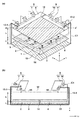
放射線検出装置は、例えば、放射線が照射される方向から見て、導電性部材13、センサアレー2及び支持基台12が重ねられて構成される。
The radiation detection device is configured, for example, by stacking the
センサアレー2は、ガラス等の絶縁性表面を有する基板で構成され、1つの画素にそれぞれが対応する複数の変換素子1及びスイッチ素子3を、二次元のアレー状に配置した平面状の放射線検出部である。センサアレー2は、スイッチ素子3を駆動するための駆動信号線4と、変換素子1による放射線の検出結果を出力させるための画像信号線5とが配線される。なお、センサアレー2においては、スイッチ素子3の構造や、駆動信号線4と画像信号線5とが交差することに起因する、意図せず形成される静電容量として、寄生容量14が存在し得る。
The
変換素子1は、放射線を電気信号に変換する素子である。スイッチ素子3はTFT等で構成される。上述のように、変換素子1とスイッチ素子3とがペアで1つの画素に対応し、このペアが、センサアレー2において、二次元のアレー状に配置されることで、複数の画素からなる放射線撮像画像を取得するための放射線検出部として機能する。駆動信号線4は、変換素子1とスイッチ素子3との組み合わせが配置される二次元のアレーにおけるそれぞれの行に対応して配置され、各行のスイッチ素子3に対して、駆動オンバイアスおよび駆動オフバイアスのいずれかを供給する。なお、駆動オフバイアスは、スイッチ素子3をオフ状態にできる電位であればよく、本実施形態では、例えば、グランドと同電位である。画像信号線5は、上述の二次元のアレーにおけるそれぞれの列ごとに配置され、駆動信号線4により駆動オンバイアスが供給されたスイッチ素子3に対応する変換素子1の電気信号、すなわち放射線の検出結果を、読み出し回路6へ伝達する。なお、変換素子1は、放射線を電気信号に直接変換する直接変換型のものと、不図示の蛍光体が放射線の照射を受けたことに応じて発する光を電気信号に変換する間接変換型のものとの、いずれであってもよい。
The conversion element 1 is an element that converts radiation into an electric signal. The switch element 3 is composed of a TFT or the like. As described above, the conversion element 1 and the switching element 3 are paired to correspond to one pixel, and this pair is arranged in the
読み出し回路6及び出力回路9は、支持基台12に配置される。支持基台12は、センサアレー2、読み出し回路6および出力回路9を固定し支持するための基台である。支持基台12は、導電性の金属または、昨今の軽量化の要望に対し、軽量かつ強度の高い炭素繊維強化プラスチック(CFRP)で金属メッシュを挟み込んだもの、あるいはCFRP単体等が用いられる。なお、支持基台12と、駆動信号線4及び画像信号線5は、衝撃緩衝のための部材や各種回路を放射線から遮蔽するための遮蔽部材により、放射線照射方向、すなわちZ方向に対向する面において間隔hを隔てて配置されている。
The
読み出し回路6は、センスアンプ7と読み出し基板8とを含んで構成され、放射線の検出結果を取得するための取得回路として機能する。センスアンプ7は、画像信号線5からの電気信号をA/Dコンバータ等でデジタル信号に変換し、読み出し基板8へ伝送する。読み出し基板8は、例えば、センスアンプ7への制御信号の入出力を行い、場合によっては電力の供給をも行う。
The
出力回路9は、ゲートドライバ10と出力基板11とを含んで構成され、上述のスイッチ素子3のそれぞれを駆動させる駆動回路として機能する。ゲートドライバ10は、駆動信号線4へ、スイッチ素子3をオンとするための駆動オンバイアスと、オフとするための駆動オフバイアスとのいずれかを、選択的に印加する。ゲートドライバ10には、駆動オンバイアスと駆動オフバイアスとが入力されうる。出力基板11は、ゲートドライバ10への制御信号の入出力や電力の供給を行う。
The
センスアンプ7及びゲートドライバ10は一般的には集積回路で構成され、不図示のTCP(Tape Carrier Package)、COF(Chip On Film)等のフレキシブル基板に搭載される。また、COG(Chip On Glass)と呼ばれる実装方式により、センスアンプ7及びゲートドライバ10はセンサアレー2上に搭載されてもよい。
The
導電性部材13は、センサアレー2よりも放射線照射側に配置され、放射線以外の可視光の検出防止、不図示の蛍光体の保護、及び電界性のノイズ対策等の少なくともいずれかの目的で使用される。導電性部材13は、上記目的のため、通常、変換素子1、駆動信号線4および画像信号線5に近接して配置され、放射線照射方向、すなわちZ方向において、間隔h’を隔てた位置に配置される。なお、導電性部材13は、撮影時において放射線を透過させる必要があるため、例えば、放射線透過率が99%以上となる厚さであることが必要である。導電性部材13は、例えばアルミニウムを含む、センサアレー2を覆う薄膜であり、その厚さは例えば0.1〜100μm程度である。なお、導電性部材13は、これに限定されるものではなく、放射線透過率が99%以上である導電性の材料であれば、他の材料によって形成され、又は厚さが上述の範囲外であってもよい。
The
また、導電性部材13は、本実施形態では、後述するように、交流磁界ノイズを受信する閉ループの一部、すなわち誘導電流の伝搬経路の一部としても使用される。このため、導電性部材13の一部13−1および13−2が、それぞれ読み出し回路6のグランド、出力回路9のグランドと電気的に接続される。
Further, in the present embodiment, the
接続点15は、読み出し回路6および出力回路9のグランドを、支持基台12と導通させるための接続であり、導電性のビスなどを用いる。なお、本実施形態においては、例えば、読み出し回路6と出力回路9とのグランドの少なくともいずれかが、支持基台12と導通されない、すなわち電気的に接続されないように構成されうる。
The
以下、本実施形態の放射線検出装置の動作原理について説明する。図2(a)及び(b)は、比較例として、図1の放射線検出装置から、導電性部材13と読み出し回路6および出力回路9のグランドとを電気的に接続する部分である13−1および13−2が省略された場合の放射線検出装置の構成を示す図である。図2(a)は、放射線検出装置の比較例の斜視図であり、図2(b)は、図2(a)におけるb−b’の断面図である。なお、図2(a)及び(b)において、図1(a)及び(b)と同様の構成部分には同一符号を付している。
Hereinafter, the operation principle of the radiation detection apparatus of this embodiment will be described. 2A and 2B show, as a comparative example, a portion 13-1 for electrically connecting the
放射線検出装置においては、電磁誘導の法則により、放射線検出装置内の閉回路を、交流磁界、すなわち変動する磁束が貫くことにより誘導起電力が発生する。さらに、誘起された誘導起電力は、閉回路のインピーダンスにより誘導電流に変換され、その誘導電流がセンスアンプ7で検出される電気信号に重畳し、これにより画像ノイズが発生する。この誘導電流は、交流磁界ノイズの磁束密度、及び貫く閉回路の断面積に比例し、閉回路のインピーダンスに反比例することが知られている。すなわち、交流磁界ノイズが貫く閉回路の断面積が小さく、かつ、閉回路のインピーダンスが高いほど、画像ノイズが発生しにくくなる。
In the radiation detection device, an induced electromotive force is generated by an AC magnetic field, that is, a fluctuating magnetic flux, passing through a closed circuit in the radiation detection device according to the law of electromagnetic induction. Furthermore, the induced electromotive force is converted into an induced current by the impedance of the closed circuit, and the induced current is superimposed on the electric signal detected by the
放射線検出装置においては、電磁誘導の法則により、放射線検出装置内の閉回路を、交流磁界、すなわち変動する磁束が貫くことにより誘導起電力を生じ、その誘導起電力がセンスアンプ7で検出される電気信号に重畳することにより画像ノイズが発生する。この誘導起電力は、交流磁界ノイズの磁束密度および貫く閉回路の断面積に比例することが知られている。すなわち、交流磁界ノイズが貫く閉回路の断面積が大きいほど、画像ノイズを生じることになる。
In the radiation detecting device, an induced electromotive force is generated by the AC magnetic field, that is, a fluctuating magnetic flux penetrates through a closed circuit in the radiation detecting device according to the law of electromagnetic induction, and the induced electromotive force is detected by the
図2(b)において、水平方向の交流磁界ノイズが貫く閉回路C2を点線で示す。この閉回路C2は、出力基板11〜ゲートドライバ10〜駆動信号線4〜寄生容量14〜画像信号線5〜センスアンプ7〜読み出し基板8の経路と、出力回路9および読み出し回路6のグランドが接続される支持基台12を経由する経路とによって形成される。したがって、水平方向の交流磁界ノイズにより生じる画像ノイズは、図2(b)の斜線で示す断面積に比例した大きさとなる。なお、閉回路C2において斜線で示していない部分は、断面で見た場合に、支持基台12と同一の平面上に存在する部分である。すなわち、説明のために支持基台12より上部に描かれているが、実際には支持基台12と同一平面上に形成されている部分である。したがって、この部分は、水平方向において断面積を有しないか有していても微小であるため、水平方向の交流磁界ノイズが貫かないか、貫いたとしても微小な影響のみを与えるに過ぎない部分となる。なお、以下の説明においても、閉回路中で斜線によって示されていない部分については同様の理由により交流磁界ノイズが貫かない又は貫いたとしても微小な影響のみを与えるに過ぎない部分を示す。
In FIG. 2B, a closed circuit C2 through which horizontal AC magnetic field noise penetrates is indicated by a dotted line. In this closed circuit C2, the paths of the
図2(a)及び(b)では、導電性部材13は、読み出し回路6および出力回路9のグランドとそれぞれ電気的に接続する部分13−1および13−2を有しないことにより、閉回路の一部として機能しない例を示している。一方で、例えば導電性部材13の一部13−1のみが読み出し回路6のグランドに接続されていても、導電性部材13は閉回路としては機能しない。また、導電性部材13の一部13−2のみが出力回路9のグランドに接続されていても同様である。すなわち、つまり導電性部材13の一部13−1及び13−2の双方の接続がなければ、導電性部材13は閉回路として機能しない。
In FIGS. 2A and 2B, the
これに対し、本実施形態に係る放射線検出装置では、導電性部材13の一部13−1が読み出し回路6のグランドに接続され、さらに導電性部材13の一部13−2が出力回路9のグランドに接続される。これにより、水平方向の交流磁界ノイズが貫く閉回路C1は、図1(b)の点線のようになる。この閉回路C1は、出力基板11〜ゲートドライバ10〜駆動信号線4〜寄生容量14〜画像信号線5〜センスアンプ7〜読み出し基板8の経路と、出力回路9および読み出し回路6のグランドが接続される導電性部材13とを含んで形成される。すなわち、本実施形態では、導電性部材13の一部13−1および13−2が出力回路9および読み出し回路6のグランドに電気的に接続されることにより、導電性部材13を経由した閉回路C1が形成される。この閉回路C1は、これまで経路としていなかった、駆動信号線4および画像信号線5に近接して配置された導電性部材13を経路の一部として使用している。そのため、従来に比べて、斜線で示した交流磁界ノイズが鎖交する断面積が大幅に小さくなっていることがわかる。これにより水平方向の交流磁界ノイズに誘起された誘導電流の一部が、断面積の小さい閉回路C1に流れることにより、画像ノイズを大幅に低減することが可能となる。
On the other hand, in the radiation detection apparatus according to the present embodiment, a part 13-1 of the
また、駆動信号線4および画像信号線5と、支持基台12との間の距離h、および、駆動信号線4および画像信号線5と、導電性部材13との間の距離h’の関係は、h‘<hとしうる。このようにすることで、従来の閉回路であるC2の断面積よりも、本実施形態で形成される閉回路C1の方が、断面積が大幅に小さくなる。すなわち、水平方向の交流磁界ノイズに誘起された誘導電流がより小さくなり、より効果的に画像ノイズを低減することが可能となる。
Further, the relationship between the distance h between the
次に、導電率又はシート抵抗値と、面積、厚み、また、形状がメッシュ状である場合は開口率等の物理形状より算出した各部材が有するインピーダンスに注目する。支持基台12と導電性部材13において、導電性部材13のインピーダンスを、支持基台12のインピーダンスよりも低くすることで、さらに画像ノイズを低減することができる。これは、断面積の大きい閉回路C2で誘起される誘導電流を少なくし、より断面積の小さい閉回路C1への誘導電流を流すことによって得られる効果であると考えられる。
Next, attention is paid to the impedance of each member calculated from the electrical conductivity or the sheet resistance value, the area, the thickness, and the physical shape such as the aperture ratio when the shape is a mesh. By setting the impedance of the
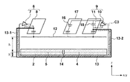
<<実施形態2>>
図3は、放射線検出装置の構造の第2の例を示す。なお、図3は、構造の断面図のみを示しているが、基本的な構造は図1(a)及び(b)と同様である。なお、本実施形態において、実施形態1と同様の構成については、同一符号を付して説明を省略する。
<<
FIG. 3 shows a second example of the structure of the radiation detection apparatus. Although FIG. 3 shows only a cross-sectional view of the structure, the basic structure is the same as that of FIGS. 1(a) and 1(b). In addition, in the present embodiment, the same configurations as those in the first embodiment are denoted by the same reference numerals and the description thereof will be omitted.
本実施形態の放射線検出装置は、駆動オフバイアスとなる電源16がゲートドライバ10に対して電源基板17を介して印加されている点において、実施形態1と異なる。駆動オフバイアスは、実施形態1ではグランド電位としたが、本実施形態では駆動オンバイアスと駆動オフバイアスの電位差がより大きくなるような電位としている。これは、駆動オフバイアスが種々のノイズにより変動した場合に、スイッチ素子3が意図せずにオンとなることを防止し、また、スイッチ素子3の漏れ電流を少なくするためのものである。また、本実施形態の放射線検出装置は、さらに、駆動オフバイアスが出力回路9上でコンデンサ18を介してグランドと接続されている点でも実施形態1と異なる。なお、コンデンサ18の容量値は、駆動オフバイアスとなる電源16のインピーダンスを鑑みて、例えば、1.3μF〜1.0mFが用いられる。
The radiation detection apparatus of this embodiment is different from that of the first embodiment in that a
図3において、実施形態1の説明と同様に、水平方向の交流磁界ノイズが貫く閉回路C3を点線で示す。閉回路C3は、出力基板11〜ゲートドライバ10〜駆動信号線4〜寄生容量14〜画像信号線5〜センスアンプ7〜読み出し基板8の経路を含む。また、閉回路C3内で、駆動オフバイアスとなっているゲートドライバ10に関して、出力回路9からコンデンサ18を介して出力回路9のグランドへ伝搬経路が形成される。そして、出力回路9および読み出し回路6のグランドが接続される導電性部材13の一部13−1および13−2によって、これらの経路と導電性部材13とを電気的に接続することにより、導電性部材13を経由した閉回路C3が形成される。
In FIG. 3, similarly to the description of the first embodiment, the closed circuit C3 through which the AC magnetic field noise in the horizontal direction penetrates is indicated by a dotted line. The closed circuit C3 includes a path from the
このように、本実施形態に係る放射線検出装置では、実施形態1と同様に、従来に比べて、斜線で示した交流磁界ノイズが鎖交する断面積が大幅に小さくなっていることがわかる。これにより水平方向の交流磁界ノイズに誘起された誘導電流の一部が、断面積の小さい閉回路C3に流れることにより、画像ノイズを大幅に低減することが可能となる。 As described above, in the radiation detection apparatus according to the present exemplary embodiment, as with the first exemplary embodiment, it is understood that the cross-sectional area where the alternating magnetic field noise shown by the diagonal lines intersects is significantly smaller than in the conventional case. As a result, a part of the induced current induced by the horizontal AC magnetic field noise flows in the closed circuit C3 having a small cross-sectional area, so that the image noise can be significantly reduced.
また、駆動信号線4および画像信号線5と、支持基台12との間の距離h、および、駆動信号線4および画像信号線5と、導電性部材13との間の距離h’の関係は、h‘<hとしうる。このようにすることで、従来の閉回路であるC2の断面積よりも、本実施形態で形成される閉回路C3の方が、断面積が大幅に小さくなる。すなわち、水平方向の交流磁界ノイズに誘起された誘導電流がより小さくなり、より効果的に画像ノイズを低減することが可能となる。
Further, the relationship between the distance h between the
さらに、支持基台12と導電性部材13において、導電性部材13のインピーダンスを、支持基台12のインピーダンスよりも低くすることで、さらに画像ノイズを低減することができる。これは、断面積の大きい閉回路C2で誘起される誘導電流を少なくし、より断面積の小さい閉回路C3への誘導電流を流すことによって得られる効果であると考えられる。
Further, in the
<<実施形態3>>
図4は、放射線検出装置の構造の第3の例を示す。なお、図4は、構造の断面図のみを示しているが、基本的な構造は図1(a)及び(b)と同様である。なお、本実施形態において、実施形態1又は2と同様の構成については、同一符号を付して説明を省略する。
<<Embodiment 3>>
FIG. 4 shows a third example of the structure of the radiation detection apparatus. Although FIG. 4 shows only a cross-sectional view of the structure, the basic structure is the same as that of FIGS. 1A and 1B. In addition, in the present embodiment, the same configurations as those of the first or second embodiment are denoted by the same reference numerals and the description thereof will be omitted.
本実施形態の放射線検出装置は、導電性部材13が、導電性部材13の一部13−2を介して駆動オフバイアスである電源16と出力回路9上で接続され、導電性部材13が駆動オフバイアスと同電位となっている点で、実施形態1及び2と異なる。また、本実施形態の放射線検出装置は、さらに、導電性部材13の一部13−1により、読み出し回路6上で、コンデンサ18を介してグランドと接続されている点で、実施形態1及び2と異なる。なお、コンデンサ18の容量値に関しては、駆動オフバイアスとなる電源16のインピーダンス等を鑑みて、例えば、1.3μF〜1.0mFが用いられる。
In the radiation detection apparatus according to the present exemplary embodiment, the
図4において、実施形態1及び2の説明と同様に、水平方向の交流磁界ノイズが貫く閉回路C4を点線で示す。閉回路C4は、ゲートドライバ10〜駆動信号線4〜寄生容量14〜画像信号線5〜センスアンプ7の経路を含む。また、閉回路C4内で、ゲートドライバ10の駆動オフバイアスへ流入または流出する電流は、出力回路9上で接続された導電性部材13の一部13−2を経由し、導電性部材13〜導電性部材13の一部13−1の経路で読み出し回路6へ到達する。この電流は読み出し回路6上のコンデンサ18を介し読み出し回路6のグランドへと到達する。以上の経路により、水平方向の交流磁界ノイズが貫く閉回路C4が形成される。
In FIG. 4, the closed circuit C4 through which the AC magnetic field noise in the horizontal direction penetrates is indicated by a dotted line, similarly to the description of the first and second embodiments. The closed circuit C4 includes a path including a
このように、本実施形態に係る放射線検出装置でも、実施形態1及び2と同様に、水平方向の交流磁界ノイズが貫く閉回路の断面積を縮小することができる。このため、本実施形態に係る放射線検出装置により、水平方向の交流磁界ノイズに起因して生じる画像ノイズを大幅に低減することができる。 As described above, also in the radiation detection apparatus according to the present exemplary embodiment, as in the first and second exemplary embodiments, it is possible to reduce the cross-sectional area of the closed circuit that the AC magnetic field noise in the horizontal direction penetrates. Therefore, the radiation detection apparatus according to the present embodiment can significantly reduce image noise caused by horizontal AC magnetic field noise.
なお、以上の各実施形態では、1つの駆動信号線4および1つの画像信号線5を経る1本の配線に対してのみ水平方向の交流磁界ノイズが貫く閉回路を点線で示したが、全ての駆動信号線4および画像信号線5の組み合わせに対して同様の閉回路が存在する。そして、これら全ての閉回路を水平方向の交流磁界ノイズが貫くことで生じた誘導起電力の積算がセンスアンプ7で検出され画像ノイズを生じる。しかしながら、上述の各実施形態に係る放射線検出装置であれば、これらの全ての駆動信号線4および画像信号線5の組み合わせに対応する全ての閉回路に対して、閉回路の断面積を縮小し、交流電磁ノイズに起因する画像ノイズを低減することができる。
In each of the above embodiments, a closed circuit in which horizontal AC magnetic field noise penetrates only one wiring passing through one
なお、上述の各実施形態に係る放射線検出装置によれば、閉回路の断面積を縮小することにより交流磁界ノイズに起因する誘導起電力を低減するものであるため、撮像時においてノイズ低減のための特段の制御は不要となる。また、鎖交する磁界ノイズの量を減らすことによる誘導起電力の低減効果であるため、交流磁界ノイズの振幅及び周波数によらずその効果を得ることが可能である。このように、上述の各実施形態の放射線検出装置によれば、外部から到来する交流磁界ノイズの周波数や振幅が未知の場合においても、撮影動作速度の低下を生じずに、水平方向の電磁ノイズによる撮影画像への影響を低減することが可能となる。 The radiation detection apparatus according to each of the above-described embodiments reduces the induced electromotive force due to the AC magnetic field noise by reducing the cross-sectional area of the closed circuit. No special control is required. Further, since it is the effect of reducing the induced electromotive force by reducing the amount of interlinking magnetic field noise, the effect can be obtained regardless of the amplitude and frequency of the AC magnetic field noise. As described above, according to the radiation detection apparatus of each of the above-described embodiments, even when the frequency or amplitude of the AC magnetic field noise coming from the outside is unknown, the imaging operation speed does not decrease and the horizontal electromagnetic noise does not occur. It is possible to reduce the influence on the captured image due to.
なお、以上の実施形態において、導電性部材13の一部13−1は、線状で読み出し回路6の一点でグランドと接続されているが、これに限定されるものではない。導電性部材13は、例えば、読み出し回路6のグランドと、複数個所で接続されてもよいし、面状に接続されてもよい。同様に、導電性部材13の一部13−2は、出力回路9のグランドと、複数個所で接続されてもよいし、面状に接続されてもよい。
In addition, in the above embodiment, the part 13-1 of the
また、上述の各実施形態では、読み出し回路6のグランドと出力回路9のグランドとの少なくともいずれかが、支持基台12に電気的に接続されないように構成することができる。これは、支持基台12をCFRPなどの導電性をほとんど持たない材料や非導電性の材料に変更することでも達成できる。つまり、支持基台12を介した閉回路のインピーダンスを無限大(又は非常に大きい値)にすることで、導電性部材13を介した閉回路のインピーダンスよりも大幅に高くすることと同等の効果を得ることができる。これにより、放射線検出装置において、支持基台12を介した閉回路が形成されることを防ぐことにより、更なる画像ノイズの低減が可能となる。
Further, in each of the above-described embodiments, at least one of the ground of the read
以下、上述の各実施形態の効果を検証するため、人体の撮影に用いるカセッテ型のX線デジタル画像撮像装置に上述の各実施形態に係る放射線検出装置を用いた場合の、ノイズ量の評価結果を示す。本評価では、X線デジタル画像撮像装置の外形寸法は384(幅)x460(奥行き)x15(厚さ)mmの物を使用した。また、変換素子はおおよそ2800x3400画素を持つ。以下の評価結果例では、外部からの水平方向の交流磁界ノイズとして、1m四方のループコイルを用いて25.04kHzの正弦波電流を印加した場合の例を示している。 Hereinafter, in order to verify the effects of each of the above-described embodiments, a noise amount evaluation result when the radiation detection apparatus according to each of the above-described embodiments is used in a cassette-type X-ray digital image capturing apparatus used for imaging a human body Indicates. In this evaluation, the external dimensions of the X-ray digital image pickup device used were 384 (width) x 460 (depth) x 15 (thickness) mm. Further, the conversion element has approximately 2800×3400 pixels. In the following evaluation result example, an example in which a sinusoidal current of 25.04 kHz is applied as a horizontal AC magnetic field noise from the outside by using a loop coil of 1 m square is shown.
[評価1]
実施形態1の放射線検出装置を用いたX線デジタル画像撮影装置において、図1(a)及び(b)における間隔h及びh’を、それぞれh=約3mm、h’=約500μmとした。また、導電性部材13の材質はアルミニウムとし、その厚さは30μmとした。また、導電性部材13は、読み出し回路6の読み出し基板8および出力回路9の出力基板11のそれぞれ一点において、導電性のビスによりグランドに電気的に接続されるものとした。
[Evaluation 1]
In the X-ray digital image capturing apparatus using the radiation detecting apparatus of the first embodiment, the intervals h and h′ in FIGS. 1A and 1B are set to h=about 3 mm and h′=about 500 μm, respectively. The material of the
このような構成において、撮影した画像ノイズ量を、比較例となる図2における画像ノイズ量と比較した。実施形態1の放射線検出装置を用いることにより、図2における画像ノイズ量を100%とした場合に、X方向からの交流磁界ノイズに起因する画像ノイズを58%に、Y方向からの交流磁界ノイズに起因する画像ノイズを87%にまで低減することができた。すなわち、実施形態1の放射線検出装置により、X方向及びY方向からの交流磁界ノイズを、それぞれ42%及び13%だけ低減する効果が得られることを確認できた。 With such a configuration, the amount of image noise captured was compared with the amount of image noise in FIG. 2, which is a comparative example. By using the radiation detection apparatus of the first embodiment, when the image noise amount in FIG. 2 is 100%, the image noise caused by the AC magnetic field noise from the X direction is 58% and the AC magnetic field noise from the Y direction. It was possible to reduce the image noise due to (1) to 87%. That is, it was confirmed that the radiation detection apparatus of the first embodiment has the effect of reducing the AC magnetic field noise from the X direction and the Y direction by 42% and 13%, respectively.
[評価2]
本評価では、評価1と異なり、実施形態1の放射線検出装置において、接続点15に非導電性の樹脂ネジ等を用いて、読み出し回路6及び出力回路9のグランドの少なくともいずれかが支持基台12と電気的に接続されないようにした。これは、支持基台12を介した閉回路のインピーダンスを無限大(又は非常に大きい値)にすることで、導電性部材13を介した閉回路のインピーダンスよりも大幅に高くすることと同等である。これにより、閉回路C1が形成される点は図1と同様であるが、誘導電流の一部が支持基台12を流れることなく、全て導電性部材13を経由した閉回路C1に流れるため、断面積低減効果をより大きくすることができるはずである。
[Evaluation 2]
In this evaluation, unlike the evaluation 1, in the radiation detection apparatus of the first embodiment, at least one of the read
このような構成において、撮影した画像ノイズ量を、比較例となる図2における画像ノイズ量と比較した。この結果、上述のような構成により、図2における画像ノイズ量を100%とした場合に、X方向からの交流磁界ノイズに起因する画像ノイズを45%に、Y方向からの交流磁界ノイズに起因する画像ノイズを87%にまで低減することができた。すなわち、実施形態1の放射線検出装置により、X方向及びY方向からの交流磁界ノイズに起因する画像ノイズを、それぞれ55%及び13%だけ低減する効果が得られることを確認できた。 With such a configuration, the amount of image noise captured was compared with the amount of image noise in FIG. 2, which is a comparative example. As a result, with the above-described configuration, when the image noise amount in FIG. 2 is 100%, the image noise due to the AC magnetic field noise from the X direction is 45% and the image noise due to the AC magnetic field noise from the Y direction. It was possible to reduce the generated image noise to 87%. That is, it was confirmed that the radiation detection apparatus of the first embodiment has an effect of reducing the image noise caused by the AC magnetic field noise from the X direction and the Y direction by 55% and 13%, respectively.
[評価3]
実施形態2の放射線検出装置をX線デジタル画像撮影装置において用いた場合についての評価を行った。本評価では、導電性部材13の一部13−1と読み出し回路6、又は導電性部材13の一部13−2と出力回路9の少なくともいずれかが電気的に接続されず、コンデンサ18が電源基板17上に実装された放射線検出装置が用いられる場合を比較対象とした。
[Evaluation 3]
The case where the radiation detection apparatus of
その結果、比較例を100%とした場合、コンデンサ18が1.3μFの場合、X方向からの交流磁界ノイズに起因する画像ノイズを90%に、Y方向からの交流磁界ノイズに起因する画像ノイズを97%にまで低減することができた。すなわち、実施形態2の放射線検出装置により、比較例と比して、X方向及びY方向からの交流磁界ノイズに起因する画像ノイズを、それぞれ10%及び3%だけ低減する効果が得られることを確認できた。
As a result, assuming that the comparative example is 100%, when the
また、コンデンサ18が69.3μFの場合において、X方向からの交流磁界ノイズに起因する画像ノイズを75%、Y方向からの交流磁界ノイズに起因する画像ノイズを71%に低減することができた。すなわち、実施形態2の放射線検出装置により、比較例と比して、X方向及びY方向からの交流磁界ノイズに起因する画像ノイズを、それぞれ25%及び29%だけ低減する効果が得られることを確認できた。
Further, when the
1:変換素子、2:センサアレー、3:スイッチ素子、4:駆動信号線、5:画像信号線、6:読み出し回路、7:センスアンプ、8:読み出し基板、9:出力回路、10:ゲートドライバ、11:出力基板、12:支持基台、13:導電性部材 1: conversion element, 2: sensor array, 3: switch element, 4: drive signal line, 5: image signal line, 6: readout circuit, 7: sense amplifier, 8: readout substrate, 9: output circuit, 10: gate Driver, 11: output substrate, 12: support base, 13: conductive member
Claims (8)
放射線に基づく電気信号を取得する素子を二次元のアレー状に配置し、照射された放射線を検出する平面状の検出手段と、
駆動信号線を介して、前記素子のそれぞれにおける前記電気信号を出力させるためのスイッチを駆動させる駆動回路と、
前記スイッチが駆動されることに応じて、画像信号線を介して、前記素子のそれぞれにおける前記電気信号を取得する取得回路と、
前記駆動回路および前記取得回路が配置される支持基台と、
前記駆動回路のグランドおよび前記取得回路のグランドと電気的に接続される導電性部材と、を有し、
放射線を照射する放射線源から見て、前記導電性部材、前記検出手段、前記支持基台の順に配置されており、前記支持基台のインピーダンスは、前記導電性部材のインピーダンスよりも高く、前記駆動回路、前記取得回路、前記駆動信号線、前記画像信号線、前記導電性部材で、閉回路が形成されていることを特徴とする放射線検出装置。 A radiation detection device,
Arrangement of elements for acquiring electric signals based on radiation in a two-dimensional array, and a flat detection means for detecting the emitted radiation,
A drive circuit for driving a switch for outputting the electric signal in each of the elements via a drive signal line ;
An acquisition circuit that acquires the electric signal in each of the elements via an image signal line in response to the switch being driven,
A support base on which the drive circuit and the acquisition circuit are arranged,
A conductive member electrically connected to the ground of the drive circuit and the ground of the acquisition circuit,
Radiation viewed from the radiation source for irradiating, the conductive member, said detecting means, said being arranged on the support base of the order, the impedance of the support base is rather higher than the impedance of the conductive member, wherein A radiation detection apparatus , wherein a closed circuit is formed by the drive circuit, the acquisition circuit, the drive signal line, the image signal line, and the conductive member .
ことを特徴とする請求項1に記載の放射線検出装置。 The support base is arranged at a position where the distance between the support base and the detection means is larger than the distance between the detection means and the conductive member.
The radiation detection apparatus according to claim 1, wherein the radiation detection apparatus is a radiation detection apparatus.
前記駆動オフバイアスと前記駆動回路のグランドとの間には、コンデンサが接続される、
ことを特徴とする請求項1または2に記載の放射線検出装置。 A drive off bias for turning off the switch is input to the drive circuit,
A capacitor is connected between the drive off bias and the ground of the drive circuit,
The radiation detecting apparatus according to claim 1, wherein the radiation detecting apparatus is a radiation detecting apparatus.
ことを特徴とする請求項3に記載の放射線検出装置。 The capacitor has a capacitance of 1.3 μF to 1.0 mF,
The radiation detecting apparatus according to claim 3, wherein the radiation detecting apparatus is a radiation detecting apparatus.
ことを特徴とする請求項1から4のいずれか1項に記載の放射線検出装置。 At least one of the ground of the drive circuit and the ground of the acquisition circuit is configured not to be electrically connected to the support base.
The radiation detection apparatus according to claim 1, wherein the radiation detection apparatus is a radiation detection apparatus.
ことを特徴とする請求項1から5のいずれか1項に記載の放射線検出装置。 Part of the conductive member has a thin film portion covering the detection means,
The radiation detecting apparatus according to claim 1, wherein the radiation detecting apparatus is a radiation detecting apparatus.
ことを特徴とする請求項1から6のいずれか1項に記載の放射線検出装置。 The conductive member, at least one of the ground of the drive circuit and the ground of the acquisition circuit, is electrically connected at a plurality of locations,
The radiation detection apparatus according to claim 1, wherein the radiation detection apparatus is a radiation detection apparatus.
前記放射線検出装置に放射線を照射する放射線源と、
前記取得回路が取得した前記電気信号に基づいて、放射線撮像画像を形成する形成装置と、
を有することを特徴とする放射線撮像システム。 A radiation detection apparatus according to any one of claims 1 to 7,
A radiation source for irradiating the radiation detection device with radiation;
A forming device for forming a radiation imaged image based on the electric signal acquired by the acquisition circuit;
A radiation imaging system comprising:
Priority Applications (8)
| Application Number | Priority Date | Filing Date | Title |
|---|---|---|---|
| EP15194996.3A EP3038349B1 (en) | 2014-12-22 | 2015-11-17 | Radiation detection apparatus and radiation imaging system |
| SG10201509711PA SG10201509711PA (en) | 2014-12-22 | 2015-11-25 | Radiation detection apparatus and radiation imaging system |
| BR102015030025A BR102015030025A2 (en) | 2014-12-22 | 2015-11-30 | radiation detection apparatus and radiation imaging system |
| US14/956,488 US9893113B2 (en) | 2014-12-22 | 2015-12-02 | Radiation detection apparatus and radiation imaging system |
| KR1020150177853A KR101967499B1 (en) | 2014-12-22 | 2015-12-14 | Radiation detection apparatus and radiation imaging system |
| CN201510946493.2A CN105708483B (en) | 2014-12-22 | 2015-12-17 | Radiation detecting apparatus and radiation imaging system |
| MYPI2015002981A MY181865A (en) | 2014-12-22 | 2015-12-17 | Radiation detection apparatus and radiation imaging system |
| PH12015000445A PH12015000445B1 (en) | 2014-12-22 | 2015-12-18 | Radiation detection apparatus and radiation imaging system |
Applications Claiming Priority (2)
| Application Number | Priority Date | Filing Date | Title |
|---|---|---|---|
| JP2014259270 | 2014-12-22 | ||
| JP2014259270 | 2014-12-22 |
Publications (3)
| Publication Number | Publication Date |
|---|---|
| JP2016118527A JP2016118527A (en) | 2016-06-30 |
| JP2016118527A5 JP2016118527A5 (en) | 2018-10-04 |
| JP6714332B2 true JP6714332B2 (en) | 2020-06-24 |
Family
ID=56244110
Family Applications (1)
| Application Number | Title | Priority Date | Filing Date |
|---|---|---|---|
| JP2015173201A Active JP6714332B2 (en) | 2014-12-22 | 2015-09-02 | Radiation detector and radiation imaging system |
Country Status (4)
| Country | Link |
|---|---|
| JP (1) | JP6714332B2 (en) |
| KR (1) | KR101967499B1 (en) |
| PH (1) | PH12015000445B1 (en) |
| SG (1) | SG10201509711PA (en) |
Families Citing this family (2)
| Publication number | Priority date | Publication date | Assignee | Title |
|---|---|---|---|---|
| JP7054356B2 (en) * | 2018-03-20 | 2022-04-13 | キヤノン株式会社 | Radiation imaging device |
| KR20240033894A (en) * | 2022-09-06 | 2024-03-13 | 주식회사 레이언스 | X-ray detector |
Family Cites Families (14)
| Publication number | Priority date | Publication date | Assignee | Title |
|---|---|---|---|---|
| US5117113A (en) * | 1990-07-06 | 1992-05-26 | Thompson And Nielson Electronics Ltd. | Direct reading dosimeter |
| JPH0784055A (en) * | 1993-06-30 | 1995-03-31 | Shimadzu Corp | Radiation two-dimensional detector |
| JP4280507B2 (en) | 2003-01-24 | 2009-06-17 | キヤノン株式会社 | Manufacturing method of radiation detection apparatus |
| JP2004363463A (en) | 2003-06-06 | 2004-12-24 | Fuji Photo Film Co Ltd | Radiation image detector |
| JP2005268271A (en) * | 2004-03-16 | 2005-09-29 | Shimadzu Corp | Two-dimensional detector for light or radiation |
| JP2005241334A (en) * | 2004-02-25 | 2005-09-08 | Shimadzu Corp | Radiation detection instrument |
| JP4671449B2 (en) * | 2004-08-10 | 2011-04-20 | キヤノン株式会社 | Radiation detection apparatus and radiation detection system |
| US20080078938A1 (en) * | 2006-10-02 | 2008-04-03 | General Electric Company | X-ray detector |
| JP5142943B2 (en) * | 2007-11-05 | 2013-02-13 | キヤノン株式会社 | Radiation detection device manufacturing method, radiation detection device and radiation imaging system |
| JP5743477B2 (en) * | 2010-09-29 | 2015-07-01 | キヤノン株式会社 | Radiography equipment |
| JP2012083170A (en) * | 2010-10-08 | 2012-04-26 | Konica Minolta Medical & Graphic Inc | Radiation image shooting device |
| JP5693174B2 (en) * | 2010-11-22 | 2015-04-01 | キヤノン株式会社 | Radiation detection apparatus and radiation detection system |
| WO2013046915A1 (en) * | 2011-09-30 | 2013-04-04 | 富士フイルム株式会社 | Radiographic imaging unit |
| JP2013250202A (en) * | 2012-06-01 | 2013-12-12 | Shimadzu Corp | Radiation detector |
-
2015
- 2015-09-02 JP JP2015173201A patent/JP6714332B2/en active Active
- 2015-11-25 SG SG10201509711PA patent/SG10201509711PA/en unknown
- 2015-12-14 KR KR1020150177853A patent/KR101967499B1/en active IP Right Grant
- 2015-12-18 PH PH12015000445A patent/PH12015000445B1/en unknown
Also Published As
| Publication number | Publication date |
|---|---|
| SG10201509711PA (en) | 2016-07-28 |
| PH12015000445A1 (en) | 2017-06-28 |
| KR101967499B1 (en) | 2019-04-09 |
| JP2016118527A (en) | 2016-06-30 |
| KR20160076446A (en) | 2016-06-30 |
| PH12015000445B1 (en) | 2017-06-28 |
Similar Documents
| Publication | Publication Date | Title |
|---|---|---|
| JP5376897B2 (en) | Radiation imaging equipment | |
| JP6574419B2 (en) | Double-sided organic photodetector on flexible substrate | |
| KR102058774B1 (en) | Radiation imaging apparatus and radiation imaging system | |
| KR102010118B1 (en) | Radiation imaging apparatus and imaging system | |
| JP5642451B2 (en) | Portable radiography equipment set, portable radiography equipment | |
| JP6801749B2 (en) | Radiation imaging device | |
| JP6381295B2 (en) | Imaging device | |
| JP6714332B2 (en) | Radiation detector and radiation imaging system | |
| JP2009300084A (en) | Radiation detection device | |
| JP6350281B2 (en) | Current / voltage conversion circuit and imaging apparatus | |
| JP5512228B2 (en) | Radiation detector | |
| US9893113B2 (en) | Radiation detection apparatus and radiation imaging system | |
| US10638059B2 (en) | Radiation detection apparatus and radiation imaging system | |
| JP6377101B2 (en) | Radiation detection apparatus and radiation detection system | |
| JP6022750B2 (en) | Radiation detector | |
| CN109073766A (en) | Flexible substrate flip chip reparation | |
| JP2012083170A (en) | Radiation image shooting device | |
| JP6590868B2 (en) | Radiation imaging apparatus and radiation imaging system | |
| JP6999447B2 (en) | Endoscope system and processor | |
| JP6548536B2 (en) | Radiation detector and X-ray CT apparatus | |
| JP2013250202A (en) | Radiation detector | |
| JP6328179B2 (en) | Radiation detection apparatus, radiation detection system, and method of manufacturing radiation detection apparatus | |
| JP2006081741A (en) | Medical diagnostic apparatus |
Legal Events
| Date | Code | Title | Description |
|---|---|---|---|
| A521 | Request for written amendment filed |
Free format text: JAPANESE INTERMEDIATE CODE: A523 Effective date: 20180823 |
|
| A621 | Written request for application examination |
Free format text: JAPANESE INTERMEDIATE CODE: A621 Effective date: 20180823 |
|
| A977 | Report on retrieval |
Free format text: JAPANESE INTERMEDIATE CODE: A971007 Effective date: 20190417 |
|
| A131 | Notification of reasons for refusal |
Free format text: JAPANESE INTERMEDIATE CODE: A131 Effective date: 20190423 |
|
| A521 | Request for written amendment filed |
Free format text: JAPANESE INTERMEDIATE CODE: A523 Effective date: 20190606 |
|
| A131 | Notification of reasons for refusal |
Free format text: JAPANESE INTERMEDIATE CODE: A131 Effective date: 20191129 |
|
| A521 | Request for written amendment filed |
Free format text: JAPANESE INTERMEDIATE CODE: A523 Effective date: 20200114 |
|
| TRDD | Decision of grant or rejection written | ||
| A01 | Written decision to grant a patent or to grant a registration (utility model) |
Free format text: JAPANESE INTERMEDIATE CODE: A01 Effective date: 20200508 |
|
| A61 | First payment of annual fees (during grant procedure) |
Free format text: JAPANESE INTERMEDIATE CODE: A61 Effective date: 20200605 |
|
| R151 | Written notification of patent or utility model registration |
Ref document number: 6714332 Country of ref document: JP Free format text: JAPANESE INTERMEDIATE CODE: R151 |