JP6574419B2 - Double-sided organic photodetector on flexible substrate - Google Patents
Double-sided organic photodetector on flexible substrate Download PDFInfo
- Publication number
- JP6574419B2 JP6574419B2 JP2016531015A JP2016531015A JP6574419B2 JP 6574419 B2 JP6574419 B2 JP 6574419B2 JP 2016531015 A JP2016531015 A JP 2016531015A JP 2016531015 A JP2016531015 A JP 2016531015A JP 6574419 B2 JP6574419 B2 JP 6574419B2
- Authority
- JP
- Japan
- Prior art keywords
- flexible substrate
- scintillator
- detection module
- photosensitive element
- photosensitive
- Prior art date
- Legal status (The legal status is an assumption and is not a legal conclusion. Google has not performed a legal analysis and makes no representation as to the accuracy of the status listed.)
- Active
Links
- 239000000758 substrate Substances 0.000 title claims description 144
- 238000001514 detection method Methods 0.000 claims description 73
- 230000005855 radiation Effects 0.000 claims description 43
- 230000005865 ionizing radiation Effects 0.000 claims description 32
- 238000003384 imaging method Methods 0.000 claims description 24
- 239000000463 material Substances 0.000 claims description 13
- 239000011368 organic material Substances 0.000 claims description 12
- 239000000853 adhesive Substances 0.000 claims description 11
- 230000001070 adhesive effect Effects 0.000 claims description 11
- 230000004044 response Effects 0.000 claims description 6
- 230000003595 spectral effect Effects 0.000 claims description 6
- 229920000642 polymer Polymers 0.000 claims description 5
- 238000000034 method Methods 0.000 description 23
- 230000008569 process Effects 0.000 description 17
- 238000004519 manufacturing process Methods 0.000 description 16
- 230000008901 benefit Effects 0.000 description 14
- 230000003287 optical effect Effects 0.000 description 14
- 238000007639 printing Methods 0.000 description 14
- 239000013078 crystal Substances 0.000 description 7
- 238000002591 computed tomography Methods 0.000 description 6
- 230000001419 dependent effect Effects 0.000 description 5
- 238000004806 packaging method and process Methods 0.000 description 5
- 239000002245 particle Substances 0.000 description 5
- 238000005452 bending Methods 0.000 description 4
- 230000000295 complement effect Effects 0.000 description 4
- 230000010354 integration Effects 0.000 description 4
- 238000013170 computed tomography imaging Methods 0.000 description 3
- 238000002059 diagnostic imaging Methods 0.000 description 3
- 239000011888 foil Substances 0.000 description 3
- 239000000976 ink Substances 0.000 description 3
- 230000003993 interaction Effects 0.000 description 3
- 238000005259 measurement Methods 0.000 description 3
- 239000004033 plastic Substances 0.000 description 3
- 229920003023 plastic Polymers 0.000 description 3
- 238000002600 positron emission tomography Methods 0.000 description 3
- 238000012545 processing Methods 0.000 description 3
- 230000035945 sensitivity Effects 0.000 description 3
- 238000002603 single-photon emission computed tomography Methods 0.000 description 3
- 239000004696 Poly ether ether ketone Substances 0.000 description 2
- 239000004642 Polyimide Substances 0.000 description 2
- 238000013459 approach Methods 0.000 description 2
- 239000011248 coating agent Substances 0.000 description 2
- 238000000576 coating method Methods 0.000 description 2
- 229920001940 conductive polymer Polymers 0.000 description 2
- 239000004020 conductor Substances 0.000 description 2
- 230000008878 coupling Effects 0.000 description 2
- 238000010168 coupling process Methods 0.000 description 2
- 238000005859 coupling reaction Methods 0.000 description 2
- 238000010586 diagram Methods 0.000 description 2
- 229920002530 polyetherether ketone Polymers 0.000 description 2
- 229920001721 polyimide Polymers 0.000 description 2
- 239000000700 radioactive tracer Substances 0.000 description 2
- 239000000126 substance Substances 0.000 description 2
- OKTJSMMVPCPJKN-UHFFFAOYSA-N Carbon Chemical compound [C] OKTJSMMVPCPJKN-UHFFFAOYSA-N 0.000 description 1
- OAICVXFJPJFONN-UHFFFAOYSA-N Phosphorus Chemical compound [P] OAICVXFJPJFONN-UHFFFAOYSA-N 0.000 description 1
- 239000004952 Polyamide Substances 0.000 description 1
- 238000003491 array Methods 0.000 description 1
- 229910052799 carbon Inorganic materials 0.000 description 1
- 239000003086 colorant Substances 0.000 description 1
- 230000000052 comparative effect Effects 0.000 description 1
- 238000013461 design Methods 0.000 description 1
- 238000011161 development Methods 0.000 description 1
- 239000013013 elastic material Substances 0.000 description 1
- 230000005670 electromagnetic radiation Effects 0.000 description 1
- 238000005516 engineering process Methods 0.000 description 1
- 238000011156 evaluation Methods 0.000 description 1
- 229920002457 flexible plastic Polymers 0.000 description 1
- 239000003292 glue Substances 0.000 description 1
- 238000011900 installation process Methods 0.000 description 1
- 150000002500 ions Chemical class 0.000 description 1
- 150000002894 organic compounds Chemical class 0.000 description 1
- 238000012858 packaging process Methods 0.000 description 1
- 238000002161 passivation Methods 0.000 description 1
- 239000002985 plastic film Substances 0.000 description 1
- 229920002647 polyamide Polymers 0.000 description 1
- 150000003071 polychlorinated biphenyls Chemical class 0.000 description 1
- 229920000307 polymer substrate Polymers 0.000 description 1
- 230000005258 radioactive decay Effects 0.000 description 1
- 230000009467 reduction Effects 0.000 description 1
- 229910052709 silver Inorganic materials 0.000 description 1
- 239000004332 silver Substances 0.000 description 1
- 238000001228 spectrum Methods 0.000 description 1
- 230000002123 temporal effect Effects 0.000 description 1
- 239000010409 thin film Substances 0.000 description 1
Images


Classifications
-
- G—PHYSICS
- G01—MEASURING; TESTING
- G01T—MEASUREMENT OF NUCLEAR OR X-RADIATION
- G01T1/00—Measuring X-radiation, gamma radiation, corpuscular radiation, or cosmic radiation
- G01T1/16—Measuring radiation intensity
- G01T1/20—Measuring radiation intensity with scintillation detectors
- G01T1/2018—Scintillation-photodiode combinations
- G01T1/20182—Modular detectors, e.g. tiled scintillators or tiled photodiodes
-
- A—HUMAN NECESSITIES
- A61—MEDICAL OR VETERINARY SCIENCE; HYGIENE
- A61B—DIAGNOSIS; SURGERY; IDENTIFICATION
- A61B6/00—Apparatus or devices for radiation diagnosis; Apparatus or devices for radiation diagnosis combined with radiation therapy equipment
- A61B6/02—Arrangements for diagnosis sequentially in different planes; Stereoscopic radiation diagnosis
- A61B6/03—Computed tomography [CT]
- A61B6/032—Transmission computed tomography [CT]
-
- A—HUMAN NECESSITIES
- A61—MEDICAL OR VETERINARY SCIENCE; HYGIENE
- A61B—DIAGNOSIS; SURGERY; IDENTIFICATION
- A61B6/00—Apparatus or devices for radiation diagnosis; Apparatus or devices for radiation diagnosis combined with radiation therapy equipment
- A61B6/02—Arrangements for diagnosis sequentially in different planes; Stereoscopic radiation diagnosis
- A61B6/03—Computed tomography [CT]
- A61B6/037—Emission tomography
-
- A—HUMAN NECESSITIES
- A61—MEDICAL OR VETERINARY SCIENCE; HYGIENE
- A61B—DIAGNOSIS; SURGERY; IDENTIFICATION
- A61B6/00—Apparatus or devices for radiation diagnosis; Apparatus or devices for radiation diagnosis combined with radiation therapy equipment
- A61B6/04—Positioning of patients; Tiltable beds or the like
- A61B6/0407—Supports, e.g. tables or beds, for the body or parts of the body
-
- A—HUMAN NECESSITIES
- A61—MEDICAL OR VETERINARY SCIENCE; HYGIENE
- A61B—DIAGNOSIS; SURGERY; IDENTIFICATION
- A61B6/00—Apparatus or devices for radiation diagnosis; Apparatus or devices for radiation diagnosis combined with radiation therapy equipment
- A61B6/44—Constructional features of apparatus for radiation diagnosis
- A61B6/4429—Constructional features of apparatus for radiation diagnosis related to the mounting of source units and detector units
- A61B6/4435—Constructional features of apparatus for radiation diagnosis related to the mounting of source units and detector units the source unit and the detector unit being coupled by a rigid structure
- A61B6/4447—Tiltable gantries
-
- G—PHYSICS
- G01—MEASURING; TESTING
- G01T—MEASUREMENT OF NUCLEAR OR X-RADIATION
- G01T1/00—Measuring X-radiation, gamma radiation, corpuscular radiation, or cosmic radiation
- G01T1/16—Measuring radiation intensity
- G01T1/20—Measuring radiation intensity with scintillation detectors
- G01T1/2018—Scintillation-photodiode combinations
- G01T1/20181—Stacked detectors, e.g. for measuring energy and positional information
-
- G—PHYSICS
- G01—MEASURING; TESTING
- G01T—MEASUREMENT OF NUCLEAR OR X-RADIATION
- G01T1/00—Measuring X-radiation, gamma radiation, corpuscular radiation, or cosmic radiation
- G01T1/16—Measuring radiation intensity
- G01T1/20—Measuring radiation intensity with scintillation detectors
- G01T1/2018—Scintillation-photodiode combinations
- G01T1/20183—Arrangements for preventing or correcting crosstalk, e.g. optical or electrical arrangements for correcting crosstalk
-
- G—PHYSICS
- G01—MEASURING; TESTING
- G01T—MEASUREMENT OF NUCLEAR OR X-RADIATION
- G01T1/00—Measuring X-radiation, gamma radiation, corpuscular radiation, or cosmic radiation
- G01T1/16—Measuring radiation intensity
- G01T1/20—Measuring radiation intensity with scintillation detectors
- G01T1/2018—Scintillation-photodiode combinations
- G01T1/20186—Position of the photodiode with respect to the incoming radiation, e.g. in the front of, below or sideways the scintillator
Landscapes
- Health & Medical Sciences (AREA)
- Life Sciences & Earth Sciences (AREA)
- Physics & Mathematics (AREA)
- High Energy & Nuclear Physics (AREA)
- Molecular Biology (AREA)
- Engineering & Computer Science (AREA)
- Medical Informatics (AREA)
- Spectroscopy & Molecular Physics (AREA)
- General Physics & Mathematics (AREA)
- Heart & Thoracic Surgery (AREA)
- Veterinary Medicine (AREA)
- Biomedical Technology (AREA)
- Pathology (AREA)
- Optics & Photonics (AREA)
- Surgery (AREA)
- Animal Behavior & Ethology (AREA)
- General Health & Medical Sciences (AREA)
- Public Health (AREA)
- Radiology & Medical Imaging (AREA)
- Biophysics (AREA)
- Nuclear Medicine, Radiotherapy & Molecular Imaging (AREA)
- Theoretical Computer Science (AREA)
- Pulmonology (AREA)
- Measurement Of Radiation (AREA)
- Nuclear Medicine (AREA)
- Apparatus For Radiation Diagnosis (AREA)
Description
本発明は、放射線源によって放出されたイオン化放射線を検出するための検出モジュールに関する。更に、本発明は、被験者の画像を提供するための撮像システムに関する。 The present invention relates to a detection module for detecting ionizing radiation emitted by a radiation source. Furthermore, the present invention relates to an imaging system for providing an image of a subject.
医療診断での実用において、1つの重要な問題は、イオン化放射線の検出に基づく患者の画像の生成である。このコンテキストで、コンピュータ断層撮像法(CT)、陽電子放射断層撮像法(PET:positron emission tomography)、及び単一光子放射コンピュータ断層撮像法(SPECT:single-photon emission computed tomography)等、様々な撮像法及びシステムが存在している。そのような撮像システムは、検出された放射線に基づく画像の生成を可能にする検出モジュールを利用する。そのための検出モジュールは通常、シンチレーション検出器(時としてシンチレータとも呼ばれる)、特にシンチレータ結晶、又はシンチレータ結晶のアレイと、光センサ(時として光検出器とも呼ばれる)とを備える。シンチレータは、入射するイオン化放射線(即ち、電子、アルファ粒子、イオン、又は高エネルギー光子等、衝突する粒子)に応答して、光フラッシュ(シンチレーション光子)を発光、即ち放出する。放出された光子は、光センサによって捕捉される。シンチレーション光子が捕捉される場所、時、及び数に基づいて、シンチレーション検出器での入射イオン化放射線の時間的及び空間的な位置並びに/又は強度が決定され得る。次いで、イオン化放射線と相互作用する物体又は撮像対象の画像を生成することが可能になる。 In practical medical diagnostics, one important issue is the generation of patient images based on the detection of ionizing radiation. In this context, various imaging methods such as computed tomography (CT), positron emission tomography (PET), and single-photon emission computed tomography (SPECT) And the system exists. Such an imaging system utilizes a detection module that enables the generation of an image based on the detected radiation. The detection module for this usually comprises a scintillation detector (sometimes also called a scintillator), in particular a scintillator crystal or an array of scintillator crystals, and a photosensor (sometimes also called a photodetector). The scintillator emits or emits a light flash (scintillation photons) in response to incident ionizing radiation (ie, colliding particles such as electrons, alpha particles, ions, or high energy photons). The emitted photons are captured by the optical sensor. Based on where, when and how many scintillation photons are captured, the temporal and spatial location and / or intensity of the incident ionizing radiation at the scintillation detector can be determined. An object that interacts with ionizing radiation or an image to be imaged can then be generated.
ここで、1つの技法は、捕捉されたイオン化放射線の強度に対応する画像を生成することに関する。エネルギー分解型撮像における1つの難点は、場合によっては高エネルギーの帯域幅の入射イオン化放射線である。CT撮像のコンテキストで、ダブルデッカー技術の開発が、エネルギー分解型CT撮像の問題を解決するための1つの選択肢である。他の技術は、例えば計数検出器である。そのようなダブルデッカー検出器は、例えば互いに重ねて取り付けられた2つのシンチレータ結晶のスタックを使用することがある。ここで、放出されたシンチレーション光の検出は、1つの画素(2つのシンチレータ結晶)の側部に取り付けられたダブルフォトダイオード(光センサ)によって達成され得る。2つのフォトダイオードはそれぞれ、隣接するシンチレータ素子の光を収集するように意図される。 Here, one technique relates to generating an image corresponding to the intensity of the captured ionizing radiation. One difficulty in energy-resolved imaging is the incident ionizing radiation, sometimes with a high energy bandwidth. In the context of CT imaging, the development of double-decker technology is one option for solving the problem of energy-resolved CT imaging. Another technique is, for example, a counting detector. Such a double-decker detector may use, for example, a stack of two scintillator crystals attached to each other. Here, the detection of the emitted scintillation light can be achieved by a double photodiode (photosensor) attached to the side of one pixel (two scintillator crystals). Each of the two photodiodes is intended to collect light from an adjacent scintillator element.
国際公開第2012/127403 A2号には、反対向きの2つの主面を有する光センサ基板を得ることを含む方法が開示されている。反対向きの2つの主面の一方は、少なくとも1つの光センサ素子の少なくとも1つの光センサ列を含み、得られる光センサ基板は、100ミクロン以上の厚さを有する。この方法は、シンチレータアレイを光センサ基板に光学的に結合することを更に含む。シンチレータアレイは、少なくとも1つの相補シンチレータ素子の少なくとも1つの相補シンチレータ列を含み、少なくとも1つの相補シンチレータ列が、少なくとも1つの光センサ列に光学的に結合され、少なくとも1つの相補シンチレータ素子が、少なくとも1つの光センサ素子に光学的に結合される。この方法は、シンチレータに光学的に結合された光センサ基板を薄くして、シンチレータに光学的に結合されており100ミクロン未満程度の厚さまで薄くされた光センサ基板を作製することを更に含む。 WO 2012/127403 A2 discloses a method that includes obtaining a photosensor substrate having two major faces opposite to each other. One of the two oppositely facing major surfaces includes at least one photosensor array of at least one photosensor element, and the resulting photosensor substrate has a thickness of 100 microns or greater. The method further includes optically coupling the scintillator array to the photosensor substrate. The scintillator array includes at least one complementary scintillator array of at least one complementary scintillator element, the at least one complementary scintillator array is optically coupled to the at least one photosensor array, and the at least one complementary scintillator element is at least It is optically coupled to one photosensor element. The method further includes thinning the photosensor substrate optically coupled to the scintillator to produce a photosensor substrate optically coupled to the scintillator and thinned to a thickness on the order of less than 100 microns.
米国特許出願公開第2013/0292574 A1号は、放射線感受性検出器アレイを含む撮像システムを開示する。シンチレータアレイ層が、基板に取り付けられたフォトダイオードの2次元アレイを含む光センサアレイ層上に提供され得る。フォトダイオードが、プラスチック又はポリアミドシート等の被膜に直接取り付けられ得ることが報告されている。代替として、薄いフォトダイオードアレイが可撓性プラスチックシートに印刷され得る。 US Patent Application Publication No. 2013/0292574 A1 discloses an imaging system that includes a radiation sensitive detector array. A scintillator array layer can be provided on the photosensor array layer comprising a two-dimensional array of photodiodes attached to a substrate. It has been reported that the photodiode can be directly attached to a coating such as a plastic or polyamide sheet. Alternatively, a thin photodiode array can be printed on a flexible plastic sheet.
米国特許出願公開第2008/0011960 A1号は、2つのパネルを有する放射線撮像装置であって、パネルがそれぞれ、基板と、信号検知素子及び読出しデバイスのアレイと、パッシベーション層と、シンチレーション蛍光体層とを含む放射線撮像装置に関する。 US Patent Application Publication No. 2008/0011960 A1 is a radiation imaging apparatus having two panels, each of which includes a substrate, an array of signal sensing elements and readout devices, a passivation layer, and a scintillation phosphor layer. The present invention relates to a radiation imaging apparatus including:
国際公開第2007/039840 A2号は、幾つかの検出器素子を有するX線検出器アレイに言及する。各検出器素子は、シンチレータと、シンチレータに光学的に結合された光検出器と、回路基板とを含む。回路基板は、ポリマー基板を含む可撓性回路でよい。しかし、そのような検出器の1つの問題は、光センサがシンチレータ素子と接触する面積が限られているため、効率、即ち集光効率が制限され得ることである。これに対する取り得る補償手段は、結晶の他の面に適切な反射材を塗布することを含むが、これは、材料及び組立てコストに関して不利である。更に、イオン化放射線に対して感受性のある面積が減少され得る。更に、光センサを垂直シンチレータスタックに光学的に結合すること、及びまた光センサをタイル基板にパッケージングして接続することにより生じる光クロストーク(即ち、1つのシンチレータ素子によって放出されたシンチレーション光子が、このシンチレータ素子の読出しのために意図されたものとは別の感光素子によって検出される)に対処するために、より費用のかかる改良されたパッケージングプロセスが必要となり得る。 WO 2007/039840 A2 refers to an X-ray detector array having several detector elements. Each detector element includes a scintillator, a photodetector optically coupled to the scintillator, and a circuit board. The circuit board may be a flexible circuit including a polymer substrate. However, one problem with such detectors is that the efficiency, i.e., light collection efficiency, can be limited because the area where the photosensor contacts the scintillator element is limited. Possible compensation measures for this include applying an appropriate reflector to the other side of the crystal, which is disadvantageous in terms of material and assembly costs. Furthermore, the area sensitive to ionizing radiation can be reduced. In addition, optical crosstalk (ie, scintillation photons emitted by one scintillator element are generated by optically coupling the optical sensor to the vertical scintillator stack and also packaging and connecting the optical sensor to the tile substrate. , Detected by a separate photosensitive element different from that intended for readout of the scintillator element) may require a more expensive and improved packaging process.
本発明の目的は、特に費用対効果の高い組立て、より良いパッケージング、及び再現性に関して、放射線源によって放出された電磁放射を検出するための改良された検出モジュールを提供することである。更に、本発明の目的は、対応する撮像システムを提供することである。 An object of the present invention is to provide an improved detection module for detecting electromagnetic radiation emitted by a radiation source, particularly with regard to cost-effective assembly, better packaging, and reproducibility. Furthermore, it is an object of the present invention to provide a corresponding imaging system.
本発明の第1の態様では、放射線源によって放出されたイオン化放射線を検出するための検出モジュールが提示される。前記検出モジュールは、入射イオン化放射線に応答してシンチレーション光子を放出するためのシンチレータ素子と、シンチレーション光子を捕捉するためにシンチレータ素子に光学的に結合された第1の感光素子と、第1の感光素子を支持するためのフレキシブル基板とを備える。フレキシブル基板は、シンチレータ素子の周りに折り曲げられて、シンチレータ素子の少なくとも2つの表面をカバーする。 In a first aspect of the invention, a detection module for detecting ionizing radiation emitted by a radiation source is presented. The detection module includes a scintillator element for emitting scintillation photons in response to incident ionizing radiation, a first photosensitive element optically coupled to the scintillator element for capturing the scintillation photon, and a first photosensitive element. And a flexible substrate for supporting the element. The flexible substrate is folded around the scintillator element to cover at least two surfaces of the scintillator element.
本発明の第2の態様では、撮像デバイスが提示される。前記撮像デバイスは、検査領域内で被験者を支持するための被験者支持体と、検査領域の第1の側に、又は検査領域内の被験者内に配置された、イオン化放射線を放出するための放射線源と、放射線源によって放出されたイオン化放射線を検出するための、検査領域の第2の側に配置された上記の検出モジュールと、検出されたイオン化放射線のスペクトル分布に基づいて画像を提供するための撮像ユニットとを備える。 In a second aspect of the invention, an imaging device is presented. The imaging device includes a subject support for supporting the subject within the examination region, and a radiation source for emitting ionizing radiation disposed on the first side of the examination region or within the subject within the examination region A detection module disposed on the second side of the examination region for detecting ionizing radiation emitted by the radiation source, and for providing an image based on the spectral distribution of the detected ionizing radiation. An imaging unit.
本発明の好ましい実施形態は、従属請求項で定義される。特許請求される撮像デバイスは、特許請求される検出モジュール、及び従属請求項で定義されるものと同様及び/又は同一の好ましい実施形態を有することを理解されたい。 Preferred embodiments of the invention are defined in the dependent claims. It is to be understood that the claimed imaging device has a preferred embodiment similar and / or identical to that defined in the claimed detection module and dependent claims.
本発明は、医療又は他の撮像用途で特に重要である。そのような撮像用途では、何らかの種類の放射線源が、イオン化放射線を放出し、即ち、原子又は分子から電子を解放し、それにより原子又は分子をイオン化するのに十分に高い個々の運動エネルギーを有する粒子を含む放射線を放出する。特に、撮像のコンテキストでのイオン化放射線は、ガンマ線又はUV線を表す。この放射線を放出する放射線源は、特に、CT又はX線撮像で使用されるX線管又は粒子加速器を表すことがある。しかし、放射線源は、例えばPET又はSPECT撮像で使用されるような、放射性崩壊プロセスにより粒子を放出する放射性トレーサ物質を表すこともある。放出されたこのイオン化放射線は、シンチレータ素子によって捕捉され、シンチレータ素子は、それに応答してシンチレーション光子を放出する。ここで、シンチレータ素子は、入射(イオン化)放射線に応答して光を放出するシンチレータ結晶を表す。本発明のコンテキストでは、シンチレータ素子は、例えば、GOS、CWO、LYSO、BGO、YAG等の無機結晶を含むことがある。 The present invention is particularly important in medical or other imaging applications. In such imaging applications, some type of radiation source emits ionizing radiation, i.e. has an individual kinetic energy high enough to release electrons from the atom or molecule, thereby ionizing the atom or molecule. Releases radiation containing particles. In particular, ionizing radiation in the context of imaging represents gamma rays or UV rays. This radiation emitting source may represent an x-ray tube or particle accelerator used in particular in CT or x-ray imaging. However, the radiation source may represent a radioactive tracer material that emits particles by a radioactive decay process, such as used in PET or SPECT imaging. This emitted ionizing radiation is captured by the scintillator element, which emits scintillation photons in response. Here, the scintillator element represents a scintillator crystal that emits light in response to incident (ionized) radiation. In the context of the present invention, the scintillator element may comprise inorganic crystals such as GOS, CWO, LYSO, BGO, YAG, for example.
シンチレータ素子によって放出される光、即ちシンチレーション光子は、シンチレータ素子に光学的に結合された感光素子によって捕捉される。そのような感光素子は、前記感光素子が結合されているシンチレータ素子が入射イオン化放射線を受けているかどうかを示すために使用され得る。通常、感光素子は、専用の読出し電子回路によって読み出され、光の量、即ち捕捉されたシンチレーション光子の数が決定される(光子計数又は電荷集積)。次いで、それに基づいて、入射イオン化放射線の分布を再構成し、画像を再構成することが可能になる。 Light emitted by the scintillator element, i.e. scintillation photons, is captured by a photosensitive element optically coupled to the scintillator element. Such a photosensitive element can be used to indicate whether the scintillator element to which the photosensitive element is coupled is receiving incident ionizing radiation. Typically, the photosensitive element is read by dedicated readout electronics to determine the amount of light, i.e. the number of scintillation photons captured (photon counting or charge integration). Based on that, it is then possible to reconstruct the distribution of incident ionizing radiation and reconstruct the image.
本発明によれば、感光素子を支持するためのフレキシブル基板が更に含まれる。本明細書で使用されるとき、フレキシブル基板は、特に、従来のプリント回路基板(PCB)等のリジッド基板とは対照的に、フレックス回路又はフレックス箔を表す。従って、フレキシブル基板は、電子接続線、構成要素、又はデバイスの集積を可能にする屈曲可能又はねじり可能な材料を表す。従来のPCBと共に使用されることを本来意図されている電子構成要素が使用される場合でさえ、少なくとも幾らかの可撓性が保たれ得る。フレキシブル基板は、特に、ポリイミド(PI)、ポリエーテルエーテルケトン(PEEK)等の可撓性有機又はプラスチック基板を表す。 According to the present invention, a flexible substrate for supporting the photosensitive element is further included. As used herein, a flexible substrate represents a flex circuit or flex foil, especially in contrast to a rigid substrate such as a conventional printed circuit board (PCB). Thus, a flexible substrate represents a bendable or twistable material that allows for the integration of electronic connecting lines, components, or devices. Even when electronic components originally intended for use with conventional PCBs are used, at least some flexibility can be maintained. The flexible substrate particularly represents a flexible organic or plastic substrate such as polyimide (PI) or polyetheretherketone (PEEK).
従来の検出モジュールと比較して、本発明による検出モジュールは、フレキシブル基板がより効率の良い組立てプロセスを可能にするという利点を有する。特に基板を屈曲することによって、基板を適切な取付け位置に容易に置くことが可能であるので、そのようなフレキシブル基板及びそれによって支持された感光素子と読出し電子回路との接続(機械的及び電気的接続)が簡素化され得る。それにより、費用のかかる取付けプロセス及び/又は検出モジュールのパッケージングのコストが大幅に削減され得る。更に、可撓性(特に有機)基板の使用は、より高いパッケージング密度をもたらすことがある。 Compared to a conventional detection module, the detection module according to the invention has the advantage that the flexible substrate allows a more efficient assembly process. In particular, by bending the substrate, it is possible to easily place the substrate in an appropriate mounting position. Therefore, the connection between the flexible substrate and the photosensitive element supported thereby and the readout electronic circuit (mechanical and electrical) Connection) can be simplified. Thereby, the costly installation process and / or the packaging cost of the detection module can be significantly reduced. Furthermore, the use of flexible (especially organic) substrates may result in higher packaging density.
更に、フレキシブル基板及びそれによって支持された電子構成要素は、同様に屈曲された状態の(例えば角部の周りで屈曲された又は非平坦面に接続された)他の構成要素(例えばシンチレータ素子)と接続(即ち接触)され得る。 In addition, the flexible substrate and the electronic components supported thereby are also similarly bent (eg, bent around corners or connected to non-flat surfaces) (eg, scintillator elements) Can be connected (ie, contacted).
好ましい実施形態では、検出モジュールは、シンチレーション光子を捕捉するための第2の感光素子を更に備え、フレキシブル基板が実質的に平らであり、第1の感光素子が、実質的に平らなフレキシブル基板の第1の表面に位置され、第2の感光素子が、第1の表面とは反対側の実質的に平らなフレキシブル基板の第2の表面に位置される。この実施形態によれば、フレキシブル基板は、その2つの表面それぞれに2つの感光素子を支持する。ここで、第1の感光素子は、やはりシンチレータ素子に接続され、放出されたシンチレーション光子をこのシンチレータ素子で捕捉する。このとき、フレキシブル基板の反対側の表面にある第2の感光素子は、第1のシンチレータ素子に並べて配置された別のシンチレータ素子に結合され得て、フレキシブル基板及び2つの感光素子がこれらのシンチレータ素子の間に挟まれる。それにより、フレキシブル基板の両側で、シンチレータ素子からの光、即ちシンチレーション光子の収集が可能になる。従って、2つのシンチレータ素子が、共通の機械的支持構造によって読み出され得る。どちらの感光素子も、個々に読み出され得る。更に、幾つかの用途では、両面に感光素子を備える検出モジュール(両面モジュール)も有利であり得、例えば、一方の側での光の量と他方の側からの光の量とを比べて測定するためのバランスセンサ用に、両側からの光が同時に収集され得る。 In a preferred embodiment, the detection module further comprises a second photosensitive element for capturing scintillation photons, wherein the flexible substrate is substantially flat and the first photosensitive element is a substantially flat flexible substrate. Located on the first surface, the second photosensitive element is located on the second surface of the substantially flat flexible substrate opposite the first surface. According to this embodiment, the flexible substrate supports two photosensitive elements on each of its two surfaces. Here, the first photosensitive element is also connected to the scintillator element, and the emitted scintillation photons are captured by the scintillator element. At this time, the second photosensitive element on the surface on the opposite side of the flexible substrate can be coupled to another scintillator element arranged side by side with the first scintillator element, and the flexible substrate and the two photosensitive elements are connected to these scintillators. It is sandwiched between elements. Thereby, light from the scintillator element, that is, scintillation photons can be collected on both sides of the flexible substrate. Thus, the two scintillator elements can be read out by a common mechanical support structure. Both photosensitive elements can be read individually. In addition, for some applications, a detection module (double-sided module) with photosensitive elements on both sides may be advantageous, for example by measuring the amount of light on one side and the amount of light on the other side. For the balance sensor to do so, light from both sides can be collected simultaneously.
別の実施形態によれば、第1及び/又は第2の感光素子が、実質的に有機材料、特にポリマーからなる。有機電子回路は、特に、無機導体ではなく導電性ポリマーを使用する。そのような導電性ポリマーは通常、より軽量であり、可撓性を提供する。感光素子は、特に、有機フォトダイオードでよい。そのような有機ダイオードは通常、フレキシブル基板上に堆積された有機化合物の被膜又は層からなる。感光素子に有機材料を使用する1つの特定の利点は、非常に薄い可撓性の構成が実現され得ることである。本出願で使用される「実質的に」は、特に、少なくとも90%、好ましくは95%、又はより好ましくは99%超等の高いパーセンテージ(このコンテキストでは、無機支持構造と比べた有機材料の高いパーセンテージ)を表し得る。フレキシブル基板と組み合わせて有機フォトダイオードを使用することは、可撓性を有する屈曲可能な光検出アセンブリを実現可能にする。これは、例えば角部又は縁部の周りで光検出アセンブリを屈曲させることによって、一平面でのみならず、様々な側からシンチレータ素子をカバーすることが可能になるという利点を生み出し得る。 According to another embodiment, the first and / or second photosensitive element consists essentially of an organic material, in particular a polymer. Organic electronic circuits in particular use conductive polymers rather than inorganic conductors. Such conductive polymers are usually lighter and provide flexibility. The photosensitive element may in particular be an organic photodiode. Such organic diodes usually consist of a coating or layer of an organic compound deposited on a flexible substrate. One particular advantage of using organic materials in the photosensitive element is that a very thin flexible configuration can be realized. As used in this application, “substantially” is a high percentage, particularly at least 90%, preferably 95%, or more preferably over 99% (in this context, higher organic materials compared to inorganic support structures). Percentage). Using an organic photodiode in combination with a flexible substrate makes it possible to realize a flexible and bendable light detection assembly. This may create the advantage that it is possible to cover the scintillator element from various sides as well as in one plane, for example by bending the light detection assembly around corners or edges.
好ましくは、フレキシブル基板は、実質的に有機材料、特にポリマーからなる。フレキシブル基板にポリマーを使用することは、容易に且つ効率良く基板を所望の幾何形状に製造することを可能にする。それにより、様々な幾何形状が可能である。 Preferably, the flexible substrate consists essentially of an organic material, in particular a polymer. The use of a polymer for the flexible substrate allows the substrate to be easily and efficiently manufactured to the desired geometry. Thereby, various geometric shapes are possible.
検出モジュールの別の実施形態では、フレキシブル基板は、シンチレーション光子がフレキシブル基板を通過するのを防ぐために不透明層を含む、又は実質的に不透明材料からなる。フレキシブル基板が不透明である場合、光クロストーク、即ち感光素子が結合されているシンチレータ素子とは別のシンチレータ素子によって放出されるシンチレーション光子の検出が減少される、又は更には完全になくされる。それにより、(光学的に)不透明な層がフレキシブル基板内に含まれること、又は基板全体が不透明材料から(実質的に)形成されることが可能である。既知の解決策では、しばしば、シンチレータ素子の1つ又は複数の表面に反射材を含むことによって比較的多量の光クロストークが補償されたが、これは、コストを増加し、製造又は組立てプロセスをより複雑にする可能性がある。それとは対照的に、本発明は、そのような反射材を必要としないことによってコストの削減を可能にし得る。更に、検出器モジュールの感光面積が増加され得るので、効率が高められ得る。シンチレーション光子がフレキシブル基板を通過するのを防ぐことが、基板の両方の表面にある2つの感光素子を独立して操作することを可能にする。第1の感光素子に結合されたシンチレータ素子によって放出されたシンチレーション光子は、フレキシブル基板の別の面に位置された第2の感光素子によっては捕捉されない。 In another embodiment of the detection module, the flexible substrate includes an opaque layer or consists essentially of an opaque material to prevent scintillation photons from passing through the flexible substrate. If the flexible substrate is opaque, the detection of optical crosstalk, i.e. scintillation photons emitted by a scintillator element separate from the scintillator element to which the photosensitive element is coupled, is reduced or even completely eliminated. Thereby, an (optical) opaque layer can be included in the flexible substrate, or the entire substrate can be (substantially) formed from an opaque material. Known solutions often compensate for a relatively large amount of optical crosstalk by including a reflector on one or more surfaces of the scintillator element, but this increases the cost and reduces the manufacturing or assembly process. May be more complicated. In contrast, the present invention may allow cost savings by not requiring such a reflector. Furthermore, the photosensitive area of the detector module can be increased, so that efficiency can be increased. Preventing scintillation photons from passing through the flexible substrate allows the two photosensitive elements on both surfaces of the substrate to be operated independently. Scintillation photons emitted by a scintillator element coupled to the first photosensitive element are not captured by a second photosensitive element located on another side of the flexible substrate.
更に別の実施形態では、第1及び/又は第2の感光素子がフレキシブル基板に印刷される。有機電子回路を使用する1つの利点は、様々な基板上に電気デバイスを製造するための印刷法を使用することが可能であることである。それにより、例えば電気的機能を有する電子又は光学インクによって、薄膜電子回路が印刷され得る。そのようなインクは通常、炭素をベースとし、しばしば導電性ラインを印刷するために銀又は他の導電性材料を混ぜてある。それにより、1つ又は複数の感光素子をフレキシブル基板の1つ又は複数の面又は表面に印刷することが可能であり得る。それにより、感光素子の様々な幾何形状及び配置が可能である。更に、感光素子がフレキシブル基板の両方の表面に印刷される2面印刷プロセスを使用することが可能である。この印刷プロセスは、順次に、即ち1面ずつ印刷するものでも、並行して、即ち両面に同時に印刷するものでもよい。また、所要の接続回路構成を印刷することも可能である。別の利点は、印刷が、製造コストの削減を可能にし得ることである。 In yet another embodiment, the first and / or second photosensitive element is printed on a flexible substrate. One advantage of using organic electronic circuits is that it is possible to use printing methods for manufacturing electrical devices on various substrates. Thereby, thin-film electronic circuits can be printed, for example, with electronic or optical ink having an electrical function. Such inks are usually based on carbon and are often mixed with silver or other conductive material to print conductive lines. Thereby, it may be possible to print one or more photosensitive elements on one or more sides or surfaces of the flexible substrate. Thereby, various geometric shapes and arrangements of the photosensitive elements are possible. Furthermore, it is possible to use a two-sided printing process in which the photosensitive elements are printed on both surfaces of the flexible substrate. This printing process may be performed sequentially, i.e. printing one page at a time, or in parallel, i.e. printing on both sides simultaneously. It is also possible to print a required connection circuit configuration. Another advantage is that printing may allow manufacturing costs to be reduced.
好ましい実施形態では、フレキシブル基板は、第1の感光素子を支持するための第1の支持層と、第2の感光素子を支持するための第2の支持層とを含み、第1の支持層と第2の支持層とが、接着剤によって、特に第1の支持層と第2の支持層との間に不透明層を形成する光絶縁接着剤によって互いに取り付けられる。フレキシブル基板の2つの面又は表面に感光素子を印刷するのとは対照的に、それぞれ1つの感光素子を支持する2つの層を備える基板を利用することも可能である。それにより、2面製造プロセス、即ち感光素子をフレキシブル基板の両面(表面)に取り付ける又は印刷することを可能にするプロセスを使用する必要はない。基板が2つの層を含む場合、これら2つの層は、接着剤によって互いに取り付けられ得て、通常、これら2つの層は、実質的に平らであり、1つの表面に感光素子を有し、感光素子を有さない表面同士で互いに接着される。ここで、不透光性接着剤を活用することが特に有利であり、この接着剤は、不透明層を形成し、フレキシブル基板の一方の側で放出されたシンチレーション光子が様々な層を通ってフレキシブル基板の他方の側に達すること(光クロストーク)を防止する。様々な層(即ち特に2つ以上の層)からフレキシブル基板を製造する1つの利点は、製造コストが削減され得ることである。更に、フレキシブル基板上の1つ又は複数の感光素子の幾何形状及び配置に関して大きな自由度を得ることが可能であり得る。 In a preferred embodiment, the flexible substrate includes a first support layer for supporting the first photosensitive element, and a second support layer for supporting the second photosensitive element, and the first support layer. And the second support layer are attached to each other by an adhesive, in particular by a photo-insulating adhesive that forms an opaque layer between the first support layer and the second support layer. In contrast to printing the photosensitive elements on the two sides or surfaces of the flexible substrate, it is also possible to utilize a substrate with two layers each supporting one photosensitive element. Thereby, it is not necessary to use a two-sided manufacturing process, i.e. a process that allows the photosensitive element to be attached or printed on both sides (surfaces) of the flexible substrate. If the substrate includes two layers, the two layers can be attached to each other by an adhesive, and typically the two layers are substantially flat, have a photosensitive element on one surface, and are photosensitive. The surfaces having no element are bonded to each other. Here, it is particularly advantageous to utilize a non-translucent adhesive, which forms an opaque layer and allows the scintillation photons emitted on one side of the flexible substrate to be flexible through various layers. Reaching the other side of the substrate (optical crosstalk) is prevented. One advantage of manufacturing a flexible substrate from various layers (ie, particularly two or more layers) is that manufacturing costs can be reduced. Further, it may be possible to obtain a great degree of freedom with respect to the geometry and arrangement of one or more photosensitive elements on the flexible substrate.
検出モジュールの別の実施形態では、シンチレータ素子は、放射線源に面する第1の表面を有して、実質的に立方形状であり、フレキシブル基板は、前記第1の表面に直交して配置されたシンチレータ素子の第2の表面に平行に配置される。この実施形態によれば、フレキシブル基板は、シンチレータ素子に平行に配置される。従って、入射放射線は通常、立方形状のシンチレータ素子の1つの表面に衝突し、シンチレータ素子内でのシンチレーション光子の放出を引き起こす。これらのシンチレーション光子は、側面、即ち放射線源の方向に直交する表面に結合された感光素子によって検出される。また、立方形状のシンチレータ素子の残りの表面の1つ又は複数において反射材を使用することも可能であり得る。この構成の1つの利点は、やはり効率的な製造が可能であることである。第1のシンチレータ素子によって放出されたシンチレーション光子を捕捉するために1つの表面に感光素子が取り付けられた1つのフレキシブル基板を使用し、そのフレキシブル基板の第2の表面に第2の感光素子を取り付け、フレキシブル基板の他方の側にあるシンチレータ素子によって放出されたシンチレーション光子を第2の感光素子によって捕捉することが可能になる。 In another embodiment of the detection module, the scintillator element has a first surface facing the radiation source and has a substantially cubic shape, and the flexible substrate is arranged perpendicular to the first surface. The scintillator element is disposed in parallel to the second surface. According to this embodiment, the flexible substrate is arranged in parallel to the scintillator element. Thus, incident radiation typically impinges on one surface of the cubic scintillator element, causing scintillation photon emission within the scintillator element. These scintillation photons are detected by a photosensitive element coupled to the side, i.e., the surface orthogonal to the direction of the radiation source. It may also be possible to use a reflector on one or more of the remaining surfaces of the cubic scintillator element. One advantage of this configuration is that it can still be efficiently manufactured. A single flexible substrate having a photosensitive element attached to one surface is used to capture scintillation photons emitted by the first scintillator element, and a second photosensitive element is attached to the second surface of the flexible substrate. The scintillation photons emitted by the scintillator element on the other side of the flexible substrate can be captured by the second photosensitive element.
更に別の実施形態では、上述したような検出モジュールは、入射イオン化放射線のスペクトル分布に関する情報を提供するための読出し電子回路を更に備え、フレキシブル基板が、感光素子を読出し電子回路に接続するための接続回路構成を含む。通常、読出し電子回路は感光素子に接続され、捕捉された放射線又は放出されたシンチレーション光子のスペクトル分布を表す情報、即ち読出値の提供を可能にする。そのような読出し電子回路は、特に、捕捉されたシンチレーション光子のデジタル表現を決定するためのアナログ−デジタル変換器を備えることができる。読出し電子回路は、好ましくは、放射線源とは反対側に配置され得て、放射線がシンチレータ素子に衝突するのを妨げず、且つ読出し電子回路での直接の検出を防ぐ。フレキシブル基板によって支持された感光素子は通常、フレキシブル基板内に集積された接続回路構成によってフレキシブル基板に接続される。そのような接続回路構成は、特に、完全に又は部分的に有機材料から形成され得、及び/又はフレキシブル基板に印刷され得る。しかし、従来の接続回路構成が従来のデバイスを含むことも可能であり得る。 In yet another embodiment, the detection module as described above further comprises readout electronics for providing information regarding the spectral distribution of the incident ionizing radiation, wherein the flexible substrate is for connecting the photosensitive element to the readout electronics. Includes connection circuit configuration. Typically, readout electronics are connected to the photosensitive element and allow the provision of information representing the spectral distribution of captured radiation or emitted scintillation photons, i.e. readout values. Such readout electronics can in particular comprise an analog-to-digital converter for determining a digital representation of the captured scintillation photons. The readout electronics can preferably be placed on the opposite side of the radiation source so as not to prevent the radiation from colliding with the scintillator element and prevent direct detection with the readout electronics. The photosensitive element supported by the flexible substrate is usually connected to the flexible substrate by a connection circuit configuration integrated in the flexible substrate. Such a connection circuit arrangement can in particular be formed completely or partly from an organic material and / or printed on a flexible substrate. However, it may be possible for a conventional connection circuit configuration to include a conventional device.
フレキシブル基板は、シンチレータ素子の周りに折り曲げられて、シンチレータ素子の少なくとも2つの表面をカバーする。基板は、その可撓性により、シンチレータ素子、特に立方形状のシンチレータ素子の周りに折り曲げられて、シンチレータ素子の2つ(又は3つ以上)の表面をカバーすることが可能である。シンチレータ素子の角部の周りにフレキシブル基板を折り曲げる(即ち被せる又は屈曲させる)ことは、完全な360°の被覆さえ可能にし得る。実質的に立方形状のシンチレータ素子の4つの表面全てをカバーする2つのL字形の箔を使用することも可能であり得る(放射線源に面する面/表面、及び読出し電子回路に面する面/表面は通常カバーされない)。それにより、感光面積が増加され得て、即ち検出モジュールの感度が増加され得る。 The flexible substrate is folded around the scintillator element to cover at least two surfaces of the scintillator element. Due to its flexibility, the substrate can be folded around a scintillator element, in particular a cubic scintillator element, to cover two (or more) surfaces of the scintillator element. Bending (ie covering or bending) the flexible substrate around the corners of the scintillator element may allow even a full 360 ° coverage. It may also be possible to use two L-shaped foils covering all four surfaces of the substantially cubic scintillator element (surface facing the radiation source / surface and surface facing the readout electronics / The surface is usually not covered). Thereby, the photosensitive area can be increased, i.e. the sensitivity of the detection module can be increased.
別の好ましい実施形態では、検出モジュールは、第2のシンチレータ素子を更に備え、第1及び第2のシンチレータ素子が、スタックとして配置され、一方のシンチレータ素子が、放射線源と他方のシンチレータ素子との間に位置され、フレキシブル基板が、スタックの1つの側面に平行に配置される。シンチレータ素子のそのようなダブルデッカースタックは、エネルギー分解型CT撮像の分野で特に有利であり得る。それにより、物質との相互作用のコンプトン散乱成分と光電成分が区別され得て、即ち、組織のエネルギー依存減衰特性に関するより多くの情報が取得され得、及び/又は放射線エネルギーのより大きな帯域幅がカバーされ得る。通常、シンチレーション光子の検出は、2つのシンチレータ素子のスタックの側部に取り付けられたダブルフォトダイオードによって実現される。2つのフォトダイオードはそれぞれ、隣接するシンチレータ素子の光を収集する。従って、スタックの1つの側面に平行に配置されたフレキシブル基板は通常、スタックの2つのシンチレータ素子に面する2つの感光素子(及び場合によっては基板の他の面/表面にある更なる感光素子)を支持する。シンチレータ素子のスタックが、2つのシンチレータ素子の間に光学的接続層、特に光伝導接着剤の層を備えることも可能であり得る。 In another preferred embodiment, the detection module further comprises a second scintillator element, the first and second scintillator elements being arranged as a stack, wherein one scintillator element is between the radiation source and the other scintillator element. Located in between, a flexible substrate is placed parallel to one side of the stack. Such a double-decker stack of scintillator elements can be particularly advantageous in the field of energy-resolved CT imaging. Thereby, the Compton scattering component and the photoelectric component of the interaction with the substance can be distinguished, i.e. more information on the energy dependent attenuation properties of the tissue can be obtained and / or a larger bandwidth of radiation energy can be obtained. Can be covered. Usually, the detection of scintillation photons is realized by a double photodiode attached to the side of a stack of two scintillator elements. Each of the two photodiodes collects light from adjacent scintillator elements. Thus, a flexible substrate placed parallel to one side of the stack typically has two photosensitive elements facing the two scintillator elements of the stack (and possibly additional photosensitive elements on the other side / surface of the substrate). Support. It may also be possible for the stack of scintillator elements to comprise an optical connection layer, in particular a layer of photoconductive adhesive, between the two scintillator elements.
更なる実施形態では、検出モジュールは、第2のシンチレータ素子を更に備え、フレキシブル基板が、第1のシンチレータ素子と第2のシンチレータ素子との間に配置され、第1の感光素子が、第1のシンチレータ素子に光学的に結合され、第2の感光素子が、第2のシンチレータ素子に光学的に結合される。フレキシブル基板の両面に感光素子を設けてフレキシブル基板を第1と第2のシンチレータ素子の間に配置することによって、単一の基板を利用することによって2つの隣接するシンチレータ素子を効率的に読み出すことが可能になる。これは、製造コストの削減、集光効率の増加、より高いパッケージング密度の実現、及び/又は所要の接続回路構成の最小化を可能にし得る。 In a further embodiment, the detection module further comprises a second scintillator element, the flexible substrate is disposed between the first scintillator element and the second scintillator element, and the first photosensitive element is the first scintillator element. The second photosensitive element is optically coupled to the second scintillator element. By providing photosensitive elements on both sides of the flexible substrate and placing the flexible substrate between the first and second scintillator elements, two adjacent scintillator elements can be efficiently read out by using a single substrate. Is possible. This may allow for reduced manufacturing costs, increased light collection efficiency, higher packaging density, and / or minimized required connection circuitry.
別の実施形態では、検出モジュールは、第2、第3、及び第4のシンチレータ素子を更に備え、第1及び第3のシンチレータ素子が、第1のスタックとして配置され、第2及び第4のシンチレータ素子が、第2のスタックとして配置され、1つのスタックにおける一方のシンチレータ素子が、放射線源とそのスタックにおける他方のシンチレータ素子との間に位置され、フレキシブル基板が、第1のスタックと第2のスタックとの間に、第1及び第2のスタックの側面に平行に配置される。2つの隣接するスタックが、2つのスタックの間のフレキシブル基板の2つの表面/面に位置された感光素子によって読み出される。これは、一方で、各シンチレータ素子が個別に読み出され得、他方で、効率の良い製造プロセスが適用され得るという利点を有する。 In another embodiment, the detection module further comprises second, third, and fourth scintillator elements, wherein the first and third scintillator elements are arranged as a first stack, and the second and fourth The scintillator elements are arranged as a second stack, one scintillator element in one stack is positioned between the radiation source and the other scintillator element in the stack, and the flexible substrate is connected to the first stack and the second stack. Between the first and second stacks, and parallel to the side surfaces of the first and second stacks. Two adjacent stacks are read by photosensitive elements located on the two surfaces / faces of the flexible substrate between the two stacks. This has the advantage that, on the one hand, each scintillator element can be read out individually, and on the other hand an efficient manufacturing process can be applied.
更に別の実施形態では、検出モジュールは、第3及び第4の感光素子を更に備え、第1、第2、第3、第4の感光素子がそれぞれ、対応する第1、第2、第3、又は第4のシンチレータ素子と光学的に結合され、第3の感光素子が、実質的に平らなフレキシブル基板の第1の表面に位置され、第4の感光素子が、実質的に平らなフレキシブル基板の第2の表面に位置される。この場合にも、各シンチレータ素子は個別に読み出され得る。 In yet another embodiment, the detection module further comprises third and fourth photosensitive elements, the first, second, third, and fourth photosensitive elements respectively corresponding to the first, second, third. , Or optically coupled to a fourth scintillator element, wherein the third photosensitive element is located on the first surface of the substantially flat flexible substrate, and the fourth photosensitive element is substantially flat flexible Located on the second surface of the substrate. Again, each scintillator element can be read individually.
本発明の別の態様では、光子を捕捉するための第1の感光素子及び第2の感光素子と、第1の表面で第1の感光素子を支持し、第2の表面で第2の感光素子を支持するためのフレキシブル基板とを備える検出モジュールであって、フレキシブル基板、第1の感光素子、及び第2の感光素子が、実質的に有機材料からなる検出モジュールが提示される。フレキシブル基板は、シンチレータ素子の周りに折り曲げられて、シンチレータ素子の少なくとも2つの表面をカバーする。 In another aspect of the present invention, a first photosensitive element and a second photosensitive element for capturing photons, a first photosensitive element supported on a first surface, and a second photosensitive element on a second surface. A detection module including a flexible substrate for supporting an element, wherein the flexible substrate, the first photosensitive element, and the second photosensitive element are substantially made of an organic material is presented. The flexible substrate is folded around the scintillator element to cover at least two surfaces of the scintillator element.
有機材料及び製造プロセスを使用することによって、更なる用途での使用のために両面検出モジュールを設計することが可能になる。一方で、感光素子は、フレキシブル基板の両面に印刷されてよい。他方で、印刷された1つの感光素子をそれぞれ有する2つの層が一体に接着されてもよい。更に、フレキシブル基板の2つの面にある感光素子の異なる幾何形状、材料、構造、性能パラメータ、及び/又はサイズ(画素サイズ)が可能である。この検出モジュールも、本発明の様々な実施形態に関して上で説明したのと同様に設計及び変形され得る。従来の検出モジュールと比較して、そのようなモジュールは、比較的低コストで様々な異なる可能な特性を提供することが可能であり得る。高い自由度が可能とされる。そのようなモジュールの用途は、様々なスペクトルの光検知用の光学測定デバイス(ここではフレキシブル基板が基本的には透明である)、又は2つの側からの入射放射線(光子)が区別される必要がある比較測定(基本的には不透明な基板を用いる)を含むことがある。更に、測定、センサ、写真撮影、及び光検出の分野での適用が可能である。取り得る実施形態は、有機材料を含む両面センサ(モジュール)、両面積層又は印刷されたセンサ(モジュール)、及び両面印刷されたセンサ(モジュール)を含む。 By using organic materials and manufacturing processes, it is possible to design a double-sided detection module for use in further applications. On the other hand, the photosensitive element may be printed on both surfaces of the flexible substrate. On the other hand, two layers each having one printed photosensitive element may be bonded together. Furthermore, different geometries, materials, structures, performance parameters, and / or sizes (pixel sizes) of the photosensitive elements on the two sides of the flexible substrate are possible. This detection module can also be designed and modified in the same manner as described above with respect to the various embodiments of the present invention. Compared to conventional detection modules, such modules may be capable of providing a variety of different possible characteristics at a relatively low cost. A high degree of freedom is possible. The application of such a module requires that optical measurement devices for light detection of various spectra (here the flexible substrate is essentially transparent) or incident radiation (photons) from two sides should be distinguished. May include some comparative measurements (basically using an opaque substrate). Furthermore, it can be applied in the fields of measurement, sensor, photography, and light detection. Possible embodiments include double-sided sensors (modules) comprising organic materials, double-sided laminated or printed sensors (modules), and double-sided printed sensors (modules).
本発明のこれら及び他の態様は、本明細書で後述する実施形態から明らかであり、それらを参照して説明する。 These and other aspects of the invention will be apparent from and will be elucidated with reference to the embodiments described hereinafter.
図1は、医療用撮像デバイス10、特にコンピュータ断層撮像(CT)スキャナの一実施形態の全体的なレイアウトを示す。そのようなCTスキャナは通常、回転ガントリ12を含み、回転ガントリ12は、概して静止したガントリ14に取り付けられる。回転ガントリ12は、検査領域16の周りで回転するように構成される。被験者支持体18に乗せた被験者を前記検査領域16内に挿入することが可能である。放射線源20が、イオン化放射線を発生する。この放射線は、検査領域16を通過し、検査領域16の他の側で、回転可能なガントリ12に取り付けられた複数の検出モジュール22によって検出される。被験者が検査領域16内に挿入される場合、検出された放射線の評価に基づいて被験者の画像を生成することが可能である。画像の生成及び提供は通常、撮像ユニット17によって行われ、撮像ユニット17は、処理装置やコンピュータ等の処理デバイスに含まれ得る、及び/又は実装され得る。
FIG. 1 shows the overall layout of one embodiment of a
図1は、本発明の1つの例示的な適用範囲を示す。しかし、本発明は、PETやSPECT撮像等の他の撮像モダリティでも使用され得、その際、放射線源は、検査対象の被験者内に挿入された放射性トレーサ物質である。また、従来のX線撮像の分野で本発明を利用することも可能であり得る。 FIG. 1 illustrates one exemplary scope of the present invention. However, the present invention can also be used with other imaging modalities such as PET and SPECT imaging, where the radiation source is a radioactive tracer material inserted into the subject to be examined. It may also be possible to use the present invention in the field of conventional X-ray imaging.
図2は、例えば医療用撮像デバイス10で使用される(従来技術)検出モジュール22の一実施形態の全体的な構造を更に示す。そのような検出モジュール22は通常、入射するイオン化放射線に応答してシンチレーション光子を放出する複数のシンチレータ素子24を備える。矢印25は、入射イオン化放射線の方向を示す。モジュール22は、適切な支持構造26によって支持された感光素子(図2には図示せず)を更に備える。感光素子は、シンチレーション光子を検出し、通常は、入射イオン化放射線によって衝突された層を決定するための読出し電子回路28に接続される。層は、光子エネルギーに対応し、光子と層の1つとの相互作用の可能性に基づいて検出される(低エネルギーの光子は、上層と相互作用しやすく、高エネルギーの光子は、より下の層と相互作用しやすい)。感光素子は、光子計数又は電荷集積によって読み出され得る。これらの読出値に基づいて、画像が生成され得る。例示される検出モジュールは、シンチレータ素子24が(入射放射線の方向で)2つのシンチレータ素子のスタックとして配置されるので、しばしばダブルデッカー検出モジュールと呼ばれる。
FIG. 2 further illustrates the overall structure of one embodiment of the
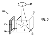
図3は、本発明による検出モジュールの第1の実施形態22aを示し、これもまた図1に示される撮像デバイス10で使用され得る。放射線源20によって放出された放射線が、シンチレータ素子24でのシンチレーション光子30の放出を引き起こす。第1の感光素子32が、シンチレータ素子24に光学的に結合され、放出されたシンチレーション光子30を捕捉する。感光素子32は、フレキシブル基板34(時としてフレックス箔とも呼ばれ、又はそれに結合された感光素子と合わせて、フレックスアレイとも呼ばれる)によって支持される。このフレキシブル基板34は通常、実質的に平らであり、放射線源20に面する表面に直交するシンチレータ素子24の側面に配置される。より分かりやすくするために、図3は、シンチレータ素子24とフレキシブル基板34又は第1の感光素子32との間に間隙を示す。第1の感光素子32がシンチレータ素子24と接触する、即ち光学的に結合されることを理解されたい。本発明によれば、フレキシブル基板34は、感光素子32を支持するために使用される。特に、実質的に有機材料からなる感光素子を支持するために、有機材料を使用することが可能である。有機電子回路又はプラスチック電子回路のこの使用は、安価であり効率の良い製造及び/又は組立てプロセスを可能にする。感光素子32は、例えば導電性インクによって基板34に印刷され得る。本発明の別の利点は、より大きな可撓性支持構造及びそれによって支持される感光素子(例えば1ステップ当たり128〜256個のダブルピクセル)の製造/組立ての容易化によって得られるものであり得る。好ましくは、感光素子32がシンチレータ素子24の1つの面に1つだけ配置される場合、シンチレーション光子30の散乱により、他の面は、それらに取り付けられた反射体(即ち反射層)を有する。シンチレータ素子24の全ての面が感光素子32によってカバーされているときにのみ、反射層が不要とされる。
FIG. 3 shows a
図4は、本発明による検出モジュールの第2の実施形態22bを示す。ここでは、フレキシブル基板34は、第1の感光素子32aに加えて、第2の感光素子32bも支持する。その際、両面製造プロセスが適用されることが可能である。特に、両面印刷プロセスが適用され得て、有機フォトダイオードが(有機)フレキシブル基板の両面に印刷され得る。
FIG. 4 shows a second embodiment 22b of a detection module according to the invention. Here, the
図5は、検出モジュールの更に別の実施形態22cを示す。ここでは、フレキシブル基板34は、複数の層を含む。両面に感光素子を有するフレキシブル基板34の製造は、2つの片面フォトダイオード−フレックスアレイ、即ち第1の支持層(36a)と第2の支持層(36b)とを一体に接着することによって実現され得る。その際、接着剤は、シンチレーション光子がフレキシブル基板34を通過するのを防ぐ不透明層37を形成することができ、光クロストークを減少する助けとなり得る。製造プロセスに応じて、(ただ1つの層を含む)フレキシブル基板の両面にフォトダイオードを印刷するための印刷プロセスを使用すること、又は(支持層を形成する)基板にフォトダイオードを印刷するために片面印刷プロセスを使用し、次いで、片面に印刷された感光素子(フォトダイオード)をそれぞれ有する2つのそのような基板を一体に接着することがより効率的であり得る。例えば電気接続用又は機械的支持用の追加の層の使用を含め、他の層構造も使用され得る。
FIG. 5 shows yet another
図6は、シンチレータ素子24の周りに被せられた又は折り曲げられた感光素子(印刷されたフォトダイオード)を支持するためのフレキシブル基板34を示す。使用される材料によっては、フレキシブル基板34は、90°の屈曲を実現し、それにより、シンチレータ素子24の2つの表面に光学的に結合された感光素子を支持することが可能である。同様にまた、これは、放射線源に面する面に直交するシンチレータ24の4つの表面全てに延長され得る。また、シンチレータ素子の4つの表面全てをカバーするために、図6に示されるL字形のフレキシブル基板が2つ使用されてもよい。どちらの方案も、完全な(又はほぼ完全な)360°の被覆、及び最適化された集光効率を実現する。シンチレータ素子の表面の1つ又は複数を一部のみカバーする等、他の方案も同様に実現され得る。
FIG. 6 shows a
また、図6には、フレキシブル基板を使用する更なる利点が示されている。フレキシブル基板34の接続のために、ただ1つの重畳相互接続部40がシンチレータ素子24に重なれば十分である。フレキシブル基板34は、シンチレータ素子24の複数の表面に光学的に結合される複数の感光素子を支持することができる。所要の接続回路が、例えば印刷プロセスによってフレキシブル基板34内に埋め込まれ得る。これは、読出し電子回路への接続点の数を減少させることができ、それにより、製造又は組立てプロセスの効率をより良くすることができる。
FIG. 6 also shows a further advantage of using a flexible substrate. For the connection of the
図7は、本発明による検出モジュールの更なる別の実施形態22dを側面視で示す。ここでは、フレキシブル基板34は、4つのシンチレータ素子44に光学的に結合される4つの感光素子42を支持する。感光素子42は、基板34の両面に印刷される。シンチレータ素子44は、シンチレータ素子の2つのスタック46a、46bとして配置される。そのようなスタック46a、46bは、特に、より高エネルギーの帯域幅のイオン化放射線を捕捉する、及び/又はイオン化放射線と物質との相互作用のコンプトン散乱成分と光電成分を区別することを可能にし得る。従って、組織のエネルギー依存減衰特性に関するより多くの情報が取得され得る。通常、スタック46a、46bの一方の2つのシンチレータ素子は、互いに光学的に結合され、例えば光伝導性接着剤によって一体に接着される。従って、イオン化放射線は、放射線源に面するシンチレータ素子を通過して、他方のシンチレータ素子によって最初は遮蔽されているシンチレータ素子内に入ることができる。入射放射線のエネルギーに応じて、シンチレータ素子それぞれでシンチレーション光子の放出が引き起こされ得る。また、他の実施形態では、1つのスタックが3つ以上のシンチレータ素子を備えること、複数のシンチレータ素子が単一の感光素子によって読み出されること、又は1つのシンチレータ素子が複数の感光素子によって読み出されることも可能であり得る。特に、複数のシンチレータ素子が1つのスタックとして配置され、各シンチレータ素子が専用の感光素子によって個別に読み出されることが有利であり得る。生成される画像において、画像の画素は、シンチレータ素子のスタックに対応する。
FIG. 7 shows a further
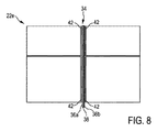
図8は、検出モジュールの別の実施形態22eを示す。ここでは、フレキシブル基板34は、それぞれ片面に感光素子42を支持する2つの支持層(基板層)36a、36bから構成される。2つの支持層36a、36bの間で、フレキシブル基板34の中央に不透光性層38が配置される。この不透光性層38は、接着剤、即ち不透光性接着剤の層でよい。層38に関する別の可能性は、例えば、提供される機械的支持を更に強化するために機械的に弾性の材料が使用され得ることである。
FIG. 8 shows another
図9は、図8で述べられるフレキシブル基板34を読出し電子回路と相互接続するための1つの取り得る手法を示す。ここでは、フレキシブル基板34及び2つの支持層36a、36bが屈曲されて、重畳相互接続部分40を形成して、検出モジュールと読出し電子回路との容易な接続を可能にする。
FIG. 9 illustrates one possible approach to interconnect the
図10及び図11は、本発明による検出モジュールの使用により得られる組立てプロセスでの1つの利点を示す。図10では、シンチレータ素子46の複数のスタックが組み立てられて検出モジュールを形成し、各スタックが個別のフレキシブル基板48を有する。それとは対照的に、図11は、読み出される必要があるシンチレータ素子46の数は同じであるが、同数の箇所に対して、読出し電子回路への90°の接続が半数だけ必要であることを示す。この90°の接続は、組立てコストに関する主要な寄与因子であり、従って、組立点の数を減少させることによって、コスト削減の大きな可能性がある。また、両面で感光素子を支持するフレキシブル基板(両面フォトダイオードアレイ)が使用される場合、必要とされる相互接続点をより少数にすることも可能であり得る。
FIGS. 10 and 11 illustrate one advantage in the assembly process obtained by using the detection module according to the present invention. In FIG. 10, a plurality of stacks of
図12は、本発明の別の態様による検出モジュール50を概略的に示す。モジュール50は、2つの表面に2つの感光素子52a、52bを有する(実質的に平らな)フレキシブル基板34を備える。モジュール50は、両側からの衝突する光子54(入射放射線)の検出を可能にする。それにより、シンチレーション光子の上述の検出とは対照的に、モジュール50は、感光素子52a、52bに使用される材料によっては、シンチレーション光子の検出を可能にするだけでなく、多少の任意の放射線54の検出も可能にする。特に、そのようなモジュール50は、有機電子回路に基づいて、例えば印刷プロセスによって製造され得て、印刷プロセスにおいて、感光素子52a、52bは、フレキシブル基板34の両面に順次に又は並行して印刷される。また、感光素子52a、52bを支持する2つ以上の層を一体に接着することも可能であり得る。
FIG. 12 schematically illustrates a
それにより、感光素子52a、52bは、用途に応じて様々な幾何形状、材料、構造、又は感度のものにすることができる。例えば、異なるスペクトル感度を有する感光素子をフレキシブル基板の1つの面又は2つの面に印刷することも可能であり得る。第1の感光素子が、第1の波長の光子の検出に適した材料を含み、第2の感光素子が、第2の波長の光子の検出に適した材料を含む場合、2色(又は、3つ以上の感光素子が使用される場合には多色)感光検出器が、比較的低コストで実現され得る。感光素子52a、52bは、光子計数又は電荷集積によって読み出され得る。
Thereby, the
フレキシブル基板は、捕捉された光子に対して透明でもそうでなくてもよい。更に、様々な特性を有する複数の層、例えば不透明層を含んでいてもよい。また、基本的にはフレキシブル基板34が感光素子52a、52bと集積されることも可能であり得る。
The flexible substrate may or may not be transparent to the captured photons. Furthermore, a plurality of layers having various characteristics, such as an opaque layer, may be included. Further, basically, it may be possible to integrate the
必要な接続回路構成が、フレキシブル基板34内、又は感光素子52a、52b内に含まれ得る。しかし、更なる印刷プロセスによって、又は従来のデバイスを含むことによって、接続回路構成が一部又は完全に集積されることも可能であり得る。製造プロセスによっては、感光素子だけでなく、光学フィルタ等の光学構造を印刷することも可能であり得る。当然、複数の感光素子がフレキシブル基板34の1つの面又は2つの面に支持されることも可能であり得、また、片面又は両面にある感光素子の異なる幾何学的構造も可能であり得る。
Necessary connection circuit configurations may be included in the
本発明を図面及び前述の説明で詳細に図示して説明してきたが、そのような図示及び説明は例示又は例説とみなすべきであり、限定とみなすべきではない。本発明は、開示される実施形態に限定されない。開示される実施形態に対する他の変形は、図面、本開示、及び添付の特許請求の範囲の検討から当業者によって理解され、特許請求される発明を実践する際に実施され得る。 While the invention has been illustrated and described in detail in the drawings and foregoing description, such illustration and description are to be considered illustrative or exemplary and not restrictive. The invention is not limited to the disclosed embodiments. Other variations to the disclosed embodiments will be understood by those skilled in the art from consideration of the drawings, the present disclosure, and the appended claims, and may be implemented in practicing the claimed invention.
特許請求の範囲において、用語「備える」は、他の要素又はステップを除外せず、不定冠詞「a」又は「an」は、複数を除外しない。単一の処理装置又は他のユニットが、特許請求の範囲に記載される幾つかの要素の機能を実現することができる。特定の手段が相互に異なる従属請求項に記載されていることだけでは、これらの手段の組合せが有利に使用され得ないことを示さない。 In the claims, the term “comprising” does not exclude other elements or steps, and the indefinite article “a” or “an” does not exclude a plurality. A single processing unit or other unit may fulfill the functions of several elements recited in the claims. The mere fact that certain measures are recited in mutually different dependent claims does not indicate that a combination of these measured cannot be used to advantage.
特許請求の範囲内の任意の参照符号は、範囲を限定するものとみなされるべきではない。 Any reference signs in the claims should not be construed as limiting the scope.
Claims (13)
入射イオン化放射線に応答してシンチレーション光子を放出するための第1のシンチレータ素子と、
シンチレーション光子を捕捉するための、前記第1のシンチレータ素子に光学的に結合された第1の感光素子と、
前記第1の感光素子を支持するためのフレキシブル基板と
を備え、
前記フレキシブル基板が、前記第1のシンチレータ素子の少なくとも2つの表面をカバーするために前記第1のシンチレータ素子の周りに折り曲げられ、前記第1の感光素子は、前記第1のシンチレータ素子の前記少なくとも2つの表面の各表面に光学的に結合される、
検出モジュール。 A detection module for detecting ionizing radiation emitted by a radiation source,
A first scintillator element for emitting scintillation photons in response to incident ionizing radiation;
A first photosensitive element optically coupled to the first scintillator element for capturing scintillation photons;
A flexible substrate for supporting the first photosensitive element,
The flexible substrate, wherein at least said to cover the two surfaces folded et al is about the first scintillator element, said first photosensitive element of the first scintillator elements, said first scintillator element Optically coupled to each of the at least two surfaces;
Detection module.
前記フレキシブル基板が実質的に平らであり、
前記第1の感光素子が、前記実質的に平らなフレキシブル基板の第1の表面に位置され、前記第2の感光素子が、前記第1の表面とは反対側の前記実質的に平らなフレキシブル基板の第2の表面に位置される、
請求項1に記載の検出モジュール。 A second photosensitive element for capturing the scintillation photons;
The flexible substrate is substantially flat;
The first photosensitive element is positioned on a first surface of the substantially flat flexible substrate, and the second photosensitive element is on the substantially flat flexible side opposite the first surface. Located on the second surface of the substrate;
The detection module according to claim 1.
前記第1の支持層と前記第2の支持層とが、接着剤によって、特に前記第1の支持層と前記第2の支持層との間に不透明層を形成する光絶縁接着剤によって互いに取り付けられる、
請求項2に記載の検出モジュール。 The flexible substrate includes a first support layer for supporting the first photosensitive element and a second support layer for supporting the second photosensitive element;
The first support layer and the second support layer are attached to each other by an adhesive, in particular by a photo-insulating adhesive that forms an opaque layer between the first support layer and the second support layer. Be
The detection module according to claim 2.
前記フレキシブル基板が、前記第1の表面に直交して配置された前記第1のシンチレータ素子の第2の表面に平行に配置される、
請求項1に記載の検出モジュール。 The first scintillator element has a first surface facing the radiation source and is substantially cubic;
The flexible substrate is disposed in parallel to a second surface of the first scintillator element disposed orthogonal to the first surface;
The detection module according to claim 1.
前記フレキシブル基板が、感光素子を前記読出し電子回路に接続するための接続回路構成を含む、
請求項1に記載の検出モジュール。 Further comprising readout electronics for providing information regarding the spectral distribution of the incident ionizing radiation;
The flexible substrate includes a connection circuit configuration for connecting a photosensitive element to the readout electronic circuit;
The detection module according to claim 1.
前記フレキシブル基板が、前記第1のシンチレータ素子と前記第2のシンチレータ素子との間に配置され、
前記第1の感光素子が、前記第1のシンチレータ素子に光学的に結合され、前記第2の感光素子が、前記第2のシンチレータ素子に光学的に結合される、
請求項2に記載の検出モジュール。 A second scintillator element;
The flexible substrate is disposed between the first scintillator element and the second scintillator element;
The first photosensitive element is optically coupled to the first scintillator element, and the second photosensitive element is optically coupled to the second scintillator element;
The detection module according to claim 2.
前記第1及び第3のシンチレータ素子が、第1のスタックとして配置され、前記第2及び第4のシンチレータ素子が、第2のスタックとして配置され、1つのスタックにおける一方のシンチレータ素子が、前記放射線源と前記スタックにおける他方のシンチレータ素子との間に位置され、
前記フレキシブル基板が、前記第1のスタックと前記第2のスタックとの間に、前記第1のスタック及び前記第2のスタックの側面に平行に配置される、
請求項2に記載の検出モジュール。 Further comprising second, third and fourth scintillator elements;
The first and third scintillator elements are arranged as a first stack, the second and fourth scintillator elements are arranged as a second stack, and one scintillator element in one stack is the radiation. Located between the source and the other scintillator element in the stack;
The flexible substrate is disposed between the first stack and the second stack in parallel to the side surfaces of the first stack and the second stack.
The detection module according to claim 2.
前記第1、第2、第3、第4の感光素子がそれぞれ、対応する前記第1、第2、第3、又は第4のシンチレータ素子と光学的に結合され、
前記第3の感光素子が、前記実質的に平らなフレキシブル基板の前記第1の表面に位置され、
前記第4の感光素子が、前記実質的に平らなフレキシブル基板の前記第2の表面に位置される、
請求項11に記載の検出モジュール。 Further comprising third and fourth photosensitive elements;
Each of the first, second, third, and fourth photosensitive elements is optically coupled to the corresponding first, second, third, or fourth scintillator element;
The third photosensitive element is positioned on the first surface of the substantially flat flexible substrate;
The fourth photosensitive element is positioned on the second surface of the substantially flat flexible substrate;
The detection module according to claim 11.
前記検査領域の第1の側に、又は前記検査領域内の前記被験者内に配置された、イオン化放射線を放出するための放射線源と、
前記放射線源によって放出されたイオン化放射線を検出するための、前記検査領域の第2の側に配置された請求項1に記載の検出モジュールと、
検出されたイオン化放射線のスペクトル分布に基づいて画像を提供するための撮像ユニットとを備える、撮像デバイス。 A subject support for supporting the subject within the examination area;
A radiation source for emitting ionizing radiation disposed on a first side of the examination region or in the subject within the examination region;
The detection module according to claim 1 disposed on a second side of the examination region for detecting ionizing radiation emitted by the radiation source;
An imaging device comprising: an imaging unit for providing an image based on a detected spectral distribution of ionizing radiation.
Applications Claiming Priority (3)
| Application Number | Priority Date | Filing Date | Title |
|---|---|---|---|
| EP13193104.0 | 2013-11-15 | ||
| EP13193104 | 2013-11-15 | ||
| PCT/EP2014/074809 WO2015071471A1 (en) | 2013-11-15 | 2014-11-17 | Double-sided organic photodetector on flexible substrate |
Publications (3)
| Publication Number | Publication Date |
|---|---|
| JP2017501388A JP2017501388A (en) | 2017-01-12 |
| JP2017501388A5 JP2017501388A5 (en) | 2017-12-28 |
| JP6574419B2 true JP6574419B2 (en) | 2019-09-11 |
Family
ID=49582661
Family Applications (1)
| Application Number | Title | Priority Date | Filing Date |
|---|---|---|---|
| JP2016531015A Active JP6574419B2 (en) | 2013-11-15 | 2014-11-17 | Double-sided organic photodetector on flexible substrate |
Country Status (5)
| Country | Link |
|---|---|
| US (1) | US10288748B2 (en) |
| EP (1) | EP3069170B1 (en) |
| JP (1) | JP6574419B2 (en) |
| CN (1) | CN105723243B (en) |
| WO (1) | WO2015071471A1 (en) |
Cited By (1)
| Publication number | Priority date | Publication date | Assignee | Title |
|---|---|---|---|---|
| US12025757B2 (en) | 2017-08-03 | 2024-07-02 | The Research Foundation For The State University Of New York | Dual-screen digital radiography with asymmetric reflective screens |
Families Citing this family (21)
| Publication number | Priority date | Publication date | Assignee | Title |
|---|---|---|---|---|
| EP2871496B1 (en) * | 2013-11-12 | 2020-01-01 | Samsung Electronics Co., Ltd | Radiation detector and computed tomography apparatus using the same |
| CN105242322A (en) * | 2014-06-25 | 2016-01-13 | 清华大学 | Detector device, dual-energy CT system and detection method applying dual-energy CT system |
| US11504079B2 (en) | 2016-11-30 | 2022-11-22 | The Research Foundation For The State University Of New York | Hybrid active matrix flat panel detector system and method |
| WO2018202465A1 (en) * | 2017-05-01 | 2018-11-08 | Koninklijke Philips N.V. | Multi-layer radiation detector |
| US10261213B2 (en) | 2017-06-07 | 2019-04-16 | General Electric Company | Apparatus and method for flexible gamma ray detectors |
| WO2019041172A1 (en) | 2017-08-30 | 2019-03-07 | Shenzhen United Imaging Healthcare Co., Ltd. | System, method, and detector module for pet imaging |
| US10302782B1 (en) * | 2017-11-15 | 2019-05-28 | Varex Imaging Corporation | Flexible detector for x-ray imaging |
| CN108562927A (en) * | 2018-03-02 | 2018-09-21 | 东莞南方医大松山湖科技园有限公司 | Detector and transmitting imaging device with the detector |
| DE102018119710A1 (en) * | 2018-08-14 | 2020-02-20 | Universität Leipzig | DEVICE AND METHOD FOR DETERMINING A WAVELENGTH OF A RADIATION |
| EP3660542A1 (en) * | 2018-11-29 | 2020-06-03 | Koninklijke Philips N.V. | Hybrid x-ray and optical detector |
| CN112068178B (en) * | 2019-06-10 | 2023-08-29 | 睿生光电股份有限公司 | Radiation sensing apparatus |
| WO2021003744A1 (en) * | 2019-07-11 | 2021-01-14 | 定垣企业有限公司 | Radiation beam detection device |
| CN110441811B (en) * | 2019-08-20 | 2021-05-04 | 上海联影医疗科技股份有限公司 | PET detector and medical imaging equipment with same |
| CN110477942B (en) * | 2019-08-20 | 2023-06-23 | 上海联影医疗科技股份有限公司 | PET detector and medical imaging equipment |
| US11762108B2 (en) * | 2020-01-21 | 2023-09-19 | LightSpin Technologies Inc. | Modular pet detector comprising a plurality of modular one-dimensional arrays of monolithic detector sub-modules |
| CN111522052B (en) * | 2020-05-13 | 2022-03-25 | 奕瑞新材料科技(太仓)有限公司 | X-ray detector structure and working method thereof |
| CN112353410B (en) * | 2020-10-26 | 2023-04-25 | 武汉联影生命科学仪器有限公司 | Miniature positron emission imaging detector and miniature positron emission imaging equipment |
| CN112834530A (en) * | 2020-12-31 | 2021-05-25 | 上海奕瑞光电子科技股份有限公司 | Double-sided X-ray detector and imaging method |
| CN113063808B (en) * | 2021-03-29 | 2024-09-03 | 卡尔蔡司工业测量技术有限公司 | Inspection system and method for inspecting at least one test object |
| FR3125891A1 (en) * | 2021-07-27 | 2023-02-03 | Trixell | Matrix photosensitive detector and method of making the photosensitive detector |
| CN113671553B (en) * | 2021-09-03 | 2024-05-31 | 南京安科医疗科技有限公司 | X-ray detection array pixel unit, manufacturing process and double-layer energy spectrum CT detector |
Family Cites Families (27)
| Publication number | Priority date | Publication date | Assignee | Title |
|---|---|---|---|---|
| DE10136756C2 (en) * | 2001-07-27 | 2003-07-31 | Siemens Ag | X-ray diagnostic device with a flexible solid-state X-ray detector |
| US7078702B2 (en) * | 2002-07-25 | 2006-07-18 | General Electric Company | Imager |
| US7618511B2 (en) * | 2003-03-07 | 2009-11-17 | Hamamatsu Photonics K.K. | Scintillator panel and method of manufacturing radiation image sensor |
| US20040227091A1 (en) * | 2003-05-14 | 2004-11-18 | Leblanc James Walter | Methods and apparatus for radiation detecting and imaging using monolithic detectors |
| JP2004354271A (en) * | 2003-05-30 | 2004-12-16 | Tohken Co Ltd | Radiation detector |
| EP1934633A2 (en) * | 2005-10-05 | 2008-06-25 | Koninklijke Philips Electronics N.V. | Computed tomography detector using thin circuits |
| US7834321B2 (en) | 2006-07-14 | 2010-11-16 | Carestream Health, Inc. | Apparatus for asymmetric dual-screen digital radiography |
| RU2445647C2 (en) * | 2006-11-17 | 2012-03-20 | Конинклейке Филипс Электроникс Н.В. | Radiation detector with multiple electrodes on sensitive layer |
| RU2468474C2 (en) | 2007-04-24 | 2012-11-27 | Конинклейке Филипс Электроникс Н.В. | Photodiodes and manufacture thereof |
| US7737407B2 (en) * | 2007-07-03 | 2010-06-15 | Siemens Medical Solutions Usa, Inc. | Method and apparatus for providing depth-of-interaction detection using positron emission tomography (PET) |
| JP5697982B2 (en) * | 2007-09-07 | 2015-04-08 | コーニンクレッカ フィリップス エヌ ヴェ | Radiation detector, X-ray detector and image forming system having a plurality of conversion layers |
| WO2009060349A2 (en) * | 2007-11-09 | 2009-05-14 | Koninklijke Philips Electronics N.V. | Protection of hygroscopic scintillators |
| US8461542B2 (en) * | 2008-09-08 | 2013-06-11 | Koninklijke Philips Electronics N.V. | Radiation detector with a stack of converter plates and interconnect layers |
| CN102216806B (en) | 2008-11-18 | 2015-08-19 | 皇家飞利浦电子股份有限公司 | spectral imaging detector |
| CN102256548B (en) * | 2008-12-17 | 2014-03-05 | 皇家飞利浦电子股份有限公司 | X-ray examination apparatus and method |
| DE102008063323A1 (en) * | 2008-12-30 | 2010-07-08 | Siemens Aktiengesellschaft | Radiation detector, light detector assembly, manufacturing method and imaging system |
| US8373132B2 (en) | 2009-02-06 | 2013-02-12 | Koninklijke Philips Electronics N. V. | Radiation detector with a stack of scintillator elements and photodiode arrays |
| EP2251713A1 (en) * | 2009-05-12 | 2010-11-17 | Ruprecht-Karls-Universität Heidelberg | Detector for verifying ionising beams |
| WO2010134993A1 (en) * | 2009-05-18 | 2010-11-25 | Sarnoff Corporation | Slab scintillator with integrated double-sided photoreceiver |
| CN102483461B (en) * | 2009-09-08 | 2015-04-29 | 皇家飞利浦电子股份有限公司 | Imaging measurement system with a printed photodetector array |
| BR112013014570A2 (en) | 2010-12-13 | 2017-07-04 | Koninl Philips Electronics Nv | radiation detector for high energy radiation detection and examination apparatus |
| EP2671097B1 (en) * | 2011-02-03 | 2016-10-19 | Koninklijke Philips N.V. | Single or multi-energy vertical radiation sensitive detectors |
| KR20120103912A (en) | 2011-03-11 | 2012-09-20 | 삼성전자주식회사 | Image sensor employing organic photoelectric conversion unit |
| EP2689269B1 (en) | 2011-03-24 | 2015-05-13 | Koninklijke Philips N.V. | Production of a spectral imaging detector |
| US9194959B2 (en) * | 2011-07-06 | 2015-11-24 | Siemens Medical Solutions Usa, Inc. | Positron emission tomography detector based on monolithic scintillator crystal |
| US8736008B2 (en) | 2012-01-04 | 2014-05-27 | General Electric Company | Photodiode array and methods of fabrication |
| US9012857B2 (en) * | 2012-05-07 | 2015-04-21 | Koninklijke Philips N.V. | Multi-layer horizontal computed tomography (CT) detector array with at least one thin photosensor array layer disposed between at least two scintillator array layers |
-
2014
- 2014-11-17 JP JP2016531015A patent/JP6574419B2/en active Active
- 2014-11-17 EP EP14799455.2A patent/EP3069170B1/en active Active
- 2014-11-17 WO PCT/EP2014/074809 patent/WO2015071471A1/en active Application Filing
- 2014-11-17 CN CN201480061806.XA patent/CN105723243B/en active Active
- 2014-11-17 US US15/035,515 patent/US10288748B2/en active Active
Cited By (1)
| Publication number | Priority date | Publication date | Assignee | Title |
|---|---|---|---|---|
| US12025757B2 (en) | 2017-08-03 | 2024-07-02 | The Research Foundation For The State University Of New York | Dual-screen digital radiography with asymmetric reflective screens |
Also Published As
| Publication number | Publication date |
|---|---|
| WO2015071471A1 (en) | 2015-05-21 |
| US10288748B2 (en) | 2019-05-14 |
| JP2017501388A (en) | 2017-01-12 |
| CN105723243B (en) | 2019-07-09 |
| EP3069170A1 (en) | 2016-09-21 |
| EP3069170B1 (en) | 2020-04-15 |
| CN105723243A (en) | 2016-06-29 |
| US20160274249A1 (en) | 2016-09-22 |
Similar Documents
| Publication | Publication Date | Title |
|---|---|---|
| JP6574419B2 (en) | Double-sided organic photodetector on flexible substrate | |
| US10591616B2 (en) | Spectral imaging detector | |
| CN104285162B (en) | Multiple-layer horizontal computer tomography (CT) detector array with least one the glimmer sensor array layer being arranged between at least two scintillator arrays layer | |
| RU2595795C2 (en) | Spectral image detector | |
| US7541593B2 (en) | Radiation detection module, printed circuit board, and radiological imaging apparatus | |
| US7081627B2 (en) | Image detector for X-ray radiation | |
| JP2008510130A (en) | Solid-state detector packaging technology | |
| JP7065843B2 (en) | Radiation detector scintillator with integrated through-hole interconnect | |
| CN103339527A (en) | Single or multi-energy vertical radiation sensitive detectors | |
| RU2647206C1 (en) | Sensor device and visualization system for detecting radiation signals | |
| EP3283903A1 (en) | Detector array for radiation system | |
| JP2009198343A (en) | Detector arrangement substrate and nuclear medicine diagnosis device using it | |
| US7283608B2 (en) | System and method for X-ray imaging using X-ray intensity information | |
| US7138632B2 (en) | Radiation detector | |
| KR20170113264A (en) | Radiation detection apparatus and radiation imaging system | |
| JP2009074817A (en) | Semiconductor detector module, and radiation detection device or nuclear medicine diagnosis device using the semiconductor detector module | |
| US11522017B2 (en) | Organic photoreceptors | |
| US20140198900A1 (en) | High resolution x-ray imaging with thin, flexible digital sensors | |
| JP4834427B2 (en) | Radiation detection module, printed circuit board, and nuclear medicine diagnostic apparatus | |
| KR101717954B1 (en) | Integrated gamma-ray and x-ray imaging detector |
Legal Events
| Date | Code | Title | Description |
|---|---|---|---|
| A521 | Request for written amendment filed |
Free format text: JAPANESE INTERMEDIATE CODE: A523 Effective date: 20171115 |
|
| A621 | Written request for application examination |
Free format text: JAPANESE INTERMEDIATE CODE: A621 Effective date: 20171115 |
|
| A977 | Report on retrieval |
Free format text: JAPANESE INTERMEDIATE CODE: A971007 Effective date: 20180927 |
|
| A131 | Notification of reasons for refusal |
Free format text: JAPANESE INTERMEDIATE CODE: A131 Effective date: 20181002 |
|
| A601 | Written request for extension of time |
Free format text: JAPANESE INTERMEDIATE CODE: A601 Effective date: 20181225 |
|
| A521 | Request for written amendment filed |
Free format text: JAPANESE INTERMEDIATE CODE: A523 Effective date: 20190329 |
|
| TRDD | Decision of grant or rejection written | ||
| A01 | Written decision to grant a patent or to grant a registration (utility model) |
Free format text: JAPANESE INTERMEDIATE CODE: A01 Effective date: 20190719 |
|
| A61 | First payment of annual fees (during grant procedure) |
Free format text: JAPANESE INTERMEDIATE CODE: A61 Effective date: 20190816 |
|
| R150 | Certificate of patent or registration of utility model |
Ref document number: 6574419 Country of ref document: JP Free format text: JAPANESE INTERMEDIATE CODE: R150 |
|
| R250 | Receipt of annual fees |
Free format text: JAPANESE INTERMEDIATE CODE: R250 |
|
| R250 | Receipt of annual fees |
Free format text: JAPANESE INTERMEDIATE CODE: R250 |
|
| R250 | Receipt of annual fees |
Free format text: JAPANESE INTERMEDIATE CODE: R250 |