JP6650389B2 - 画素、これを含むディスプレイ装置及びその制御方法 - Google Patents
画素、これを含むディスプレイ装置及びその制御方法 Download PDFInfo
- Publication number
- JP6650389B2 JP6650389B2 JP2016243973A JP2016243973A JP6650389B2 JP 6650389 B2 JP6650389 B2 JP 6650389B2 JP 2016243973 A JP2016243973 A JP 2016243973A JP 2016243973 A JP2016243973 A JP 2016243973A JP 6650389 B2 JP6650389 B2 JP 6650389B2
- Authority
- JP
- Japan
- Prior art keywords
- light emitting
- emitting diode
- transistor
- organic light
- signal
- Prior art date
- Legal status (The legal status is an assumption and is not a legal conclusion. Google has not performed a legal analysis and makes no representation as to the accuracy of the status listed.)
- Active
Links
- 238000000034 method Methods 0.000 title claims description 20
- 230000004044 response Effects 0.000 claims description 20
- 239000003990 capacitor Substances 0.000 claims description 18
- 230000008859 change Effects 0.000 claims description 9
- 230000003213 activating effect Effects 0.000 claims description 2
- 230000004913 activation Effects 0.000 claims 4
- 230000003247 decreasing effect Effects 0.000 claims 1
- 238000010586 diagram Methods 0.000 description 9
- 230000008901 benefit Effects 0.000 description 6
- 230000010354 integration Effects 0.000 description 4
- 239000003086 colorant Substances 0.000 description 3
- 150000002894 organic compounds Chemical class 0.000 description 2
- 230000008569 process Effects 0.000 description 2
- 230000006872 improvement Effects 0.000 description 1
- 239000011159 matrix material Substances 0.000 description 1
- 230000009467 reduction Effects 0.000 description 1
Images


Classifications
-
- G—PHYSICS
- G09—EDUCATION; CRYPTOGRAPHY; DISPLAY; ADVERTISING; SEALS
- G09G—ARRANGEMENTS OR CIRCUITS FOR CONTROL OF INDICATING DEVICES USING STATIC MEANS TO PRESENT VARIABLE INFORMATION
- G09G3/00—Control arrangements or circuits, of interest only in connection with visual indicators other than cathode-ray tubes
- G09G3/20—Control arrangements or circuits, of interest only in connection with visual indicators other than cathode-ray tubes for presentation of an assembly of a number of characters, e.g. a page, by composing the assembly by combination of individual elements arranged in a matrix no fixed position being assigned to or needed to be assigned to the individual characters or partial characters
- G09G3/22—Control arrangements or circuits, of interest only in connection with visual indicators other than cathode-ray tubes for presentation of an assembly of a number of characters, e.g. a page, by composing the assembly by combination of individual elements arranged in a matrix no fixed position being assigned to or needed to be assigned to the individual characters or partial characters using controlled light sources
- G09G3/30—Control arrangements or circuits, of interest only in connection with visual indicators other than cathode-ray tubes for presentation of an assembly of a number of characters, e.g. a page, by composing the assembly by combination of individual elements arranged in a matrix no fixed position being assigned to or needed to be assigned to the individual characters or partial characters using controlled light sources using electroluminescent panels
- G09G3/32—Control arrangements or circuits, of interest only in connection with visual indicators other than cathode-ray tubes for presentation of an assembly of a number of characters, e.g. a page, by composing the assembly by combination of individual elements arranged in a matrix no fixed position being assigned to or needed to be assigned to the individual characters or partial characters using controlled light sources using electroluminescent panels semiconductive, e.g. using light-emitting diodes [LED]
- G09G3/3208—Control arrangements or circuits, of interest only in connection with visual indicators other than cathode-ray tubes for presentation of an assembly of a number of characters, e.g. a page, by composing the assembly by combination of individual elements arranged in a matrix no fixed position being assigned to or needed to be assigned to the individual characters or partial characters using controlled light sources using electroluminescent panels semiconductive, e.g. using light-emitting diodes [LED] organic, e.g. using organic light-emitting diodes [OLED]
- G09G3/3225—Control arrangements or circuits, of interest only in connection with visual indicators other than cathode-ray tubes for presentation of an assembly of a number of characters, e.g. a page, by composing the assembly by combination of individual elements arranged in a matrix no fixed position being assigned to or needed to be assigned to the individual characters or partial characters using controlled light sources using electroluminescent panels semiconductive, e.g. using light-emitting diodes [LED] organic, e.g. using organic light-emitting diodes [OLED] using an active matrix
- G09G3/3233—Control arrangements or circuits, of interest only in connection with visual indicators other than cathode-ray tubes for presentation of an assembly of a number of characters, e.g. a page, by composing the assembly by combination of individual elements arranged in a matrix no fixed position being assigned to or needed to be assigned to the individual characters or partial characters using controlled light sources using electroluminescent panels semiconductive, e.g. using light-emitting diodes [LED] organic, e.g. using organic light-emitting diodes [OLED] using an active matrix with pixel circuitry controlling the current through the light-emitting element
-
- G—PHYSICS
- G09—EDUCATION; CRYPTOGRAPHY; DISPLAY; ADVERTISING; SEALS
- G09G—ARRANGEMENTS OR CIRCUITS FOR CONTROL OF INDICATING DEVICES USING STATIC MEANS TO PRESENT VARIABLE INFORMATION
- G09G2300/00—Aspects of the constitution of display devices
- G09G2300/04—Structural and physical details of display devices
- G09G2300/0439—Pixel structures
- G09G2300/0465—Improved aperture ratio, e.g. by size reduction of the pixel circuit, e.g. for improving the pixel density or the maximum displayable luminance or brightness
-
- G—PHYSICS
- G09—EDUCATION; CRYPTOGRAPHY; DISPLAY; ADVERTISING; SEALS
- G09G—ARRANGEMENTS OR CIRCUITS FOR CONTROL OF INDICATING DEVICES USING STATIC MEANS TO PRESENT VARIABLE INFORMATION
- G09G2300/00—Aspects of the constitution of display devices
- G09G2300/08—Active matrix structure, i.e. with use of active elements, inclusive of non-linear two terminal elements, in the pixels together with light emitting or modulating elements
- G09G2300/0809—Several active elements per pixel in active matrix panels
- G09G2300/0842—Several active elements per pixel in active matrix panels forming a memory circuit, e.g. a dynamic memory with one capacitor
-
- G—PHYSICS
- G09—EDUCATION; CRYPTOGRAPHY; DISPLAY; ADVERTISING; SEALS
- G09G—ARRANGEMENTS OR CIRCUITS FOR CONTROL OF INDICATING DEVICES USING STATIC MEANS TO PRESENT VARIABLE INFORMATION
- G09G2310/00—Command of the display device
- G09G2310/08—Details of timing specific for flat panels, other than clock recovery
-
- G—PHYSICS
- G09—EDUCATION; CRYPTOGRAPHY; DISPLAY; ADVERTISING; SEALS
- G09G—ARRANGEMENTS OR CIRCUITS FOR CONTROL OF INDICATING DEVICES USING STATIC MEANS TO PRESENT VARIABLE INFORMATION
- G09G2320/00—Control of display operating conditions
- G09G2320/02—Improving the quality of display appearance
- G09G2320/0233—Improving the luminance or brightness uniformity across the screen
-
- G—PHYSICS
- G09—EDUCATION; CRYPTOGRAPHY; DISPLAY; ADVERTISING; SEALS
- G09G—ARRANGEMENTS OR CIRCUITS FOR CONTROL OF INDICATING DEVICES USING STATIC MEANS TO PRESENT VARIABLE INFORMATION
- G09G2320/00—Control of display operating conditions
- G09G2320/02—Improving the quality of display appearance
- G09G2320/029—Improving the quality of display appearance by monitoring one or more pixels in the display panel, e.g. by monitoring a fixed reference pixel
- G09G2320/0295—Improving the quality of display appearance by monitoring one or more pixels in the display panel, e.g. by monitoring a fixed reference pixel by monitoring each display pixel
Description
Claims (8)
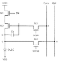
- 複数の画素を含むディスプレイ装置の制御方法において、
前記画素は、
アノード電極とカソード電極を含む有機発光ダイオード(OLED);
前記有機発光ダイオードを経由する駆動電流を供給するように構成された第1トランジスター(DT);
スキャン信号(Si)に応答してデータ信号(Dj)を前記第1トランジスター(DT)のゲートに供給するように構成された第2トランジスター(ST1);
前記データ信号(Dj)の電圧レベルと前記第1トランジスター(DT)のしきい値電圧との差を維持するように構成されたキャパシター(Cst);及び
センシング信号(SENSE)に応答して前記第1トランジスター(DT)のしきい値電圧の変化をセンシングするように構成された第3トランジスター(ST2)を含み、
前記方法は、
T1区間(T1)の間、前記スキャン信号(Si)と前記センシング信号(SENSE)とを活性化して、前記データ信号(Dj)を前記キャパシター(Cst)に伝送することと、
T2区間(T2)の間、前記スキャン信号(Si)と前記センシング信号(SENSE)とを非活性化して、前記有機発光ダイオードをオンにすることと、
前記第3トランジスター(ST2)がターンオンされる間、前記有機発光ダイオード(OLED)がターンオフされるように制御するとき、前記第3トランジスター(ST2)が受信する基準電圧(Vref)のレベルを前記有機発光ダイオード(OLED)のしきい値電圧より低く設定すること(S10)と、
T3区間(T3)の間、前記センシング信号(SENSE)を活性化させて、前記第3トランジスター(ST2)をターンオンし、前記有機発光ダイオードをターンオフさせること(S20)と、
前記センシング信号(SENSE)に応答して前記基準電圧(Vref)を前記有機発光ダイオード(OLED)のアノード電極に印加すること(S30)とを含み、
前記有機発光ダイオードの発光の活性化は、前記センシング信号の活性化によって制御され、
前記有機発光ダイオードの発光時間は、前記センシング信号の持続時間によって制御され、
前記T2区間(T2)は、前記T1区間(T1)より後にあり、前記T3区間(T3)は、前記T2区間(T2)より後にある、ディスプレイ装置の制御方法。 - 前記第1トランジスター(DT)は、前記有機発光ダイオード(OLED)と接続されて連結され、
前記第3トランジスター(ST2)がターンオンされると、前記第1トランジスター(DT)から電流が前記第3トランジスターに流れることを特徴とする、
請求項1に記載のディスプレイ装置の制御方法。 - 前記センシング信号に応答して前記基準電圧を前記有機発光ダイオードのアノード電極に印加すれば、前記有機発光ダイオードはターンオフされることを特徴とする、請求項1または2に記載のディスプレイ装置の制御方法。
- 画素を複数含むパネル(10)であって、前記画素は、データライン(Dm)とスキャンライン(Sn)との交差地点に配列され、各画素(Px)は有機発光ダイオード(OLED)を含むパネル(10);
タイミング制御ユニット(11)から提供されるスキャン制御信号(CONT1)に応答して前記スキャンライン(Sn)にスキャン信号(Si)を提供し、外部の補償のためのセンシング信号(SENSE)を前記パネルに提供するスキャン駆動部(12);
前記データライン(Dm)にデータ信号(Dj)を提供するデータ駆動部(13);及び
前記パネル(10)に高電位電圧(ELVDD)、低電位電圧(ELVSS)及び基準電圧(Vref)を提供する電源部(14)を含むディスプレイ装置であって、
前記画素は、
アノード電極とカソード電極を含む前記有機発光ダイオード(OLED);
T1区間(T1)の後のT2区間(T2)の間、前記有機発光ダイオードを経由する駆動電流を供給し、前記有機発光ダイオード(OLED)を発光させる、第1トランジスター(DT);
スキャン信号(Si)に応答してデータ信号(Dj)を前記第1トランジスター(DT)のゲートに供給する第2トランジスター(ST1)であって、前記T2区間(T2)の前の前記T1区間(T1)の間、前記スキャン信号(Si)が活性化されると、前記データ信号(Dj)を伝達する、第2トランジスター(ST1);
前記データ信号(Dj)の電圧レベルと前記第1トランジスター(DT)のしきい値電圧との差を維持するように構成されたキャパシター(Cst);及び
センシング信号(SENSE)に応答して前記第1トランジスター(DT)の前記しきい値電圧の変化をセンシングするように構成された第3トランジスター(ST2)を含み、
前記第3トランジスター(ST2)は、前記T1区間(T1)と、前記T2区間の後のT3区間との間、前記センシング信号(SENSE)が活性化されると、前記基準電圧(Vref)を前記アノード電極に連結されたノード(C)に伝送するようにさらに構成され、
前記T1区間(T1)の間、前記スキャン信号(Si)と前記センシング信号(SENSE)とが活性化されて、前記データ信号(Dj)を前記キャパシター(Cst)に伝達し、
前記T2区間(T2)の間、前記スキャン信号(Si)と前記センシング信号(SENSE)とが非活性化されて、前記有機発光ダイオードをターンオンし、
前記T3区間(T3)の間、前記スキャン信号(Si)が非活性化され、かつ前記センシング信号(SENSE)が活性化されて、前記有機発光ダイオードをターンオフし、
前記基準電圧(Vref)のレベルは前記有機発光ダイオード(OLED)のしきい値電圧より低く、
前記有機発光ダイオードの発光の活性化は、前記センシング信号の活性化によって制御され、
前記有機発光ダイオードの発光時間は、前記センシング信号の持続時間によって制御される
ディスプレイ装置。 - 前記センシング信号(SENSE)によって前記有機発光ダイオード(OLED)を経由する電流の流れの可否を決定することを特徴とする、請求項4に記載のディスプレイ装置。
- 前記センシング信号(SENSE)が活性化されると、前記基準電圧(Vref)によって前記有機発光ダイオード(OLED)がターンオフされるように制御されることを特徴とする、請求項4または5に記載のディスプレイ装置。
- 前記センシング信号(SENSE)が非活性化されると、前記第1トランジスター(DT)から前記有機発光ダイオード(OLED)に前記駆動電流が流れて前記有機発光ダイオードが発光されることを特徴とする、請求項4から6のいずれか一項に記載のディスプレイ装置。
- 前記センシング信号(SENSE)が活性化される、前記T1区間(T1)又は前記T3区間(T3)の長さは増減可能である、請求項4から7のいずれか一項に記載のディスプレイ装置。
Applications Claiming Priority (2)
| Application Number | Priority Date | Filing Date | Title |
|---|---|---|---|
| KR10-2015-0190421 | 2015-12-30 | ||
| KR1020150190421A KR102630078B1 (ko) | 2015-12-30 | 2015-12-30 | 화소, 이를 포함하는 표시 장치 및 그 제어 방법 |
Related Child Applications (1)
| Application Number | Title | Priority Date | Filing Date |
|---|---|---|---|
| JP2018233941A Division JP2019091044A (ja) | 2015-12-30 | 2018-12-14 | 画素、これを含むディスプレイ装置及びその制御方法 |
Publications (2)
| Publication Number | Publication Date |
|---|---|
| JP2017120405A JP2017120405A (ja) | 2017-07-06 |
| JP6650389B2 true JP6650389B2 (ja) | 2020-02-19 |
Family
ID=57570700
Family Applications (2)
| Application Number | Title | Priority Date | Filing Date |
|---|---|---|---|
| JP2016243973A Active JP6650389B2 (ja) | 2015-12-30 | 2016-12-16 | 画素、これを含むディスプレイ装置及びその制御方法 |
| JP2018233941A Withdrawn JP2019091044A (ja) | 2015-12-30 | 2018-12-14 | 画素、これを含むディスプレイ装置及びその制御方法 |
Family Applications After (1)
| Application Number | Title | Priority Date | Filing Date |
|---|---|---|---|
| JP2018233941A Withdrawn JP2019091044A (ja) | 2015-12-30 | 2018-12-14 | 画素、これを含むディスプレイ装置及びその制御方法 |
Country Status (6)
| Country | Link |
|---|---|
| US (1) | US10262588B2 (ja) |
| EP (2) | EP3188176A1 (ja) |
| JP (2) | JP6650389B2 (ja) |
| KR (1) | KR102630078B1 (ja) |
| CN (1) | CN106935185B (ja) |
| TW (1) | TWI628821B (ja) |
Families Citing this family (16)
| Publication number | Priority date | Publication date | Assignee | Title |
|---|---|---|---|---|
| JP6663289B2 (ja) * | 2016-04-26 | 2020-03-11 | 株式会社Joled | アクティブマトリクス表示装置 |
| KR102339821B1 (ko) * | 2017-03-13 | 2021-12-16 | 삼성디스플레이 주식회사 | 유기전계발광 표시장치 및 그의 구동방법 |
| CN107622754B (zh) * | 2017-09-22 | 2023-11-14 | 京东方科技集团股份有限公司 | 像素电路及其控制方法、显示基板、显示装置 |
| KR102582823B1 (ko) * | 2018-07-05 | 2023-09-27 | 삼성디스플레이 주식회사 | 유기 발광 표시 장치 및 이의 구동 방법 |
| KR102539517B1 (ko) * | 2018-10-11 | 2023-06-02 | 엘지디스플레이 주식회사 | 센싱 구동 회로, 디스플레이 패널 및 디스플레이 장치 |
| KR20200077197A (ko) * | 2018-12-20 | 2020-06-30 | 엘지디스플레이 주식회사 | 게이트 구동부를 포함한 전계발광 표시장치 |
| KR102566281B1 (ko) | 2019-02-18 | 2023-08-16 | 삼성디스플레이 주식회사 | 표시 장치 및 그 구동 방법 |
| CN109742134B (zh) | 2019-03-15 | 2022-07-05 | 合肥京东方卓印科技有限公司 | 有机发光二极管显示装置及其驱动方法 |
| CN110021269A (zh) * | 2019-05-05 | 2019-07-16 | 深圳市华星光电半导体显示技术有限公司 | 提升显示面板充电率的信号输入方法 |
| US20220219262A1 (en) | 2019-05-14 | 2022-07-14 | Nippon Steel Corporation | Groove processing device and groove processing method |
| CN110189701B (zh) | 2019-06-28 | 2022-07-29 | 京东方科技集团股份有限公司 | 像素驱动电路及其驱动方法、显示面板与显示装置 |
| CN110189704B (zh) * | 2019-06-28 | 2021-10-15 | 上海天马有机发光显示技术有限公司 | 一种电致发光显示面板、其驱动方法及显示装置 |
| CN110429120B (zh) * | 2019-08-05 | 2022-08-09 | 京东方科技集团股份有限公司 | 一种阵列基板、其驱动方法、显示面板及显示装置 |
| CN111261114A (zh) * | 2020-03-25 | 2020-06-09 | 京东方科技集团股份有限公司 | 显示面板及像素补偿电路 |
| KR20220009562A (ko) * | 2020-07-16 | 2022-01-25 | 엘지디스플레이 주식회사 | 표시장치와 이를 포함한 모바일 단말기 |
| US20220102475A1 (en) * | 2020-09-29 | 2022-03-31 | Tcl China Star Optoelectronics Technology Co., Ltd. | Partitioned display structure, display panel, and organic light-emitting diode display panel |
Family Cites Families (27)
| Publication number | Priority date | Publication date | Assignee | Title |
|---|---|---|---|---|
| WO2004097782A1 (en) | 2003-05-02 | 2004-11-11 | Koninklijke Philips Electronics N.V. | Active matrix oled display device with threshold voltage drift compensation |
| JP5128287B2 (ja) * | 2004-12-15 | 2013-01-23 | イグニス・イノベイション・インコーポレーテッド | 表示アレイのためのリアルタイム校正を行う方法及びシステム |
| US8576217B2 (en) | 2011-05-20 | 2013-11-05 | Ignis Innovation Inc. | System and methods for extraction of threshold and mobility parameters in AMOLED displays |
| US8004481B2 (en) | 2005-12-02 | 2011-08-23 | Semiconductor Energy Laboratory Co., Ltd. | Display device and electronic device |
| JP2009008799A (ja) * | 2007-06-27 | 2009-01-15 | Sharp Corp | 表示装置およびその駆動方法 |
| JP2009265459A (ja) * | 2008-04-28 | 2009-11-12 | Fujifilm Corp | 画素回路および表示装置 |
| KR20100034560A (ko) * | 2008-09-24 | 2010-04-01 | 삼성전자주식회사 | 표시 장치 및 그 구동 방법 |
| JP5165657B2 (ja) * | 2008-12-24 | 2013-03-21 | 株式会社ジャパンディスプレイイースト | 画像表示装置 |
| KR101388286B1 (ko) | 2009-11-24 | 2014-04-22 | 엘지디스플레이 주식회사 | 유기발광다이오드 표시장치 및 그 구동방법 |
| KR101073226B1 (ko) * | 2010-03-17 | 2011-10-12 | 삼성모바일디스플레이주식회사 | 유기전계발광 표시장치 |
| KR101739575B1 (ko) | 2010-09-28 | 2017-05-25 | 삼성디스플레이 주식회사 | 주사 구동 장치 및 그 구동 방법 |
| CN106910464B (zh) | 2011-05-27 | 2020-04-24 | 伊格尼斯创新公司 | 补偿显示器阵列中像素的系统和驱动发光器件的像素电路 |
| US9236011B2 (en) * | 2011-08-30 | 2016-01-12 | Lg Display Co., Ltd. | Organic light emitting diode display device for pixel current sensing in the sensing mode and pixel current sensing method thereof |
| US9324268B2 (en) | 2013-03-15 | 2016-04-26 | Ignis Innovation Inc. | Amoled displays with multiple readout circuits |
| KR20140066830A (ko) * | 2012-11-22 | 2014-06-02 | 엘지디스플레이 주식회사 | 유기 발광 표시 장치 |
| KR101969436B1 (ko) * | 2012-12-20 | 2019-04-16 | 엘지디스플레이 주식회사 | 유기 발광 디스플레이 장치의 구동 방법 |
| KR102007370B1 (ko) * | 2012-12-24 | 2019-08-06 | 엘지디스플레이 주식회사 | 유기 발광 디스플레이 장치와 이의 구동 방법 |
| KR20150057191A (ko) | 2013-11-18 | 2015-05-28 | 삼성디스플레이 주식회사 | 화소, 이를 포함하는 표시 장치 및 그 구동 방법 |
| KR102075920B1 (ko) | 2013-11-20 | 2020-02-11 | 엘지디스플레이 주식회사 | 유기발광 표시장치와 그의 문턱전압 보상방법 |
| KR101661016B1 (ko) * | 2013-12-03 | 2016-09-29 | 엘지디스플레이 주식회사 | 유기발광 표시장치와 그의 화질 보상방법 |
| KR102223552B1 (ko) | 2013-12-04 | 2021-03-04 | 엘지디스플레이 주식회사 | 유기 발광 표시 장치 및 그의 구동 방법 |
| JP6619137B2 (ja) * | 2013-12-06 | 2019-12-11 | 株式会社半導体エネルギー研究所 | 発光装置 |
| US9842545B2 (en) | 2013-12-20 | 2017-12-12 | Sharp Kabushiki Kaisha | Display device and method for driving same |
| KR102083458B1 (ko) | 2013-12-26 | 2020-03-02 | 엘지디스플레이 주식회사 | 유기발광 표시장치 |
| KR102091485B1 (ko) * | 2013-12-30 | 2020-03-20 | 엘지디스플레이 주식회사 | 유기 발광 표시 장치 및 그의 구동 방법 |
| KR102072403B1 (ko) * | 2013-12-31 | 2020-02-03 | 엘지디스플레이 주식회사 | 하이브리드 구동 방식 유기발광표시장치 |
| US9721502B2 (en) * | 2014-04-14 | 2017-08-01 | Apple Inc. | Organic light-emitting diode display with compensation for transistor variations |
-
2015
- 2015-12-30 KR KR1020150190421A patent/KR102630078B1/ko active IP Right Grant
-
2016
- 2016-12-16 JP JP2016243973A patent/JP6650389B2/ja active Active
- 2016-12-16 TW TW105141913A patent/TWI628821B/zh active
- 2016-12-19 EP EP16205051.2A patent/EP3188176A1/en not_active Ceased
- 2016-12-19 EP EP23187301.9A patent/EP4276811A1/en active Pending
- 2016-12-23 US US15/389,710 patent/US10262588B2/en active Active
- 2016-12-26 CN CN201611216417.7A patent/CN106935185B/zh active Active
-
2018
- 2018-12-14 JP JP2018233941A patent/JP2019091044A/ja not_active Withdrawn
Also Published As
| Publication number | Publication date |
|---|---|
| JP2017120405A (ja) | 2017-07-06 |
| CN106935185B (zh) | 2019-12-06 |
| KR20170080883A (ko) | 2017-07-11 |
| KR102630078B1 (ko) | 2024-01-26 |
| EP4276811A1 (en) | 2023-11-15 |
| CN106935185A (zh) | 2017-07-07 |
| JP2019091044A (ja) | 2019-06-13 |
| TWI628821B (zh) | 2018-07-01 |
| US10262588B2 (en) | 2019-04-16 |
| EP3188176A1 (en) | 2017-07-05 |
| TW201727962A (zh) | 2017-08-01 |
| US20170193899A1 (en) | 2017-07-06 |
Similar Documents
| Publication | Publication Date | Title |
|---|---|---|
| JP6650389B2 (ja) | 画素、これを含むディスプレイ装置及びその制御方法 | |
| JP6654363B2 (ja) | 有機発光表示装置 | |
| KR101135534B1 (ko) | 화소, 이를 이용한 표시 장치, 및 그들의 구동 방법 | |
| JP5612988B2 (ja) | 有機電界発光表示装置用画素及びこれを利用した有機電界発光表示装置 | |
| KR101928379B1 (ko) | 유기발광 다이오드 표시장치 및 그 구동방법 | |
| KR102187835B1 (ko) | 유기 발광 다이오드 표시장치 및 그 구동 방법 | |
| US9460658B2 (en) | Pixel and organic light emitting display device using the same | |
| KR101155898B1 (ko) | 유기발광 표시장치 및 그 구동 방법 | |
| KR101008438B1 (ko) | 화소 및 이를 이용한 유기전계발광 표시장치 | |
| KR20170026757A (ko) | 화소 및 그의 구동방법 | |
| KR101975489B1 (ko) | 표시장치 및 그 구동 방법 | |
| KR102578715B1 (ko) | 유기발광 표시장치 | |
| KR102206602B1 (ko) | 화소 및 이를 이용한 유기전계발광 표시장치 | |
| US9318052B2 (en) | Compensating organic light emitting diode display device and method for driving the same using two adjacent gate lines per pixel | |
| KR101964768B1 (ko) | 화소, 이를 포함하는 표시장치 및 그 구동 방법 | |
| US20140354517A1 (en) | Pixel and organic light emitting display device using the same | |
| JP2008052241A (ja) | 画素及び有機電界発光表示装置 | |
| US11114034B2 (en) | Display device | |
| KR20150055233A (ko) | 유기전계발광 표시장치 및 그의 구동방법 | |
| KR20100059316A (ko) | 화소 및 이를 이용한 유기전계발광 표시장치 | |
| KR20140141189A (ko) | 화소 및 이를 이용한 유기전계발광 표시장치 | |
| KR20140028921A (ko) | 화소 및 이를 이용한 유기전계발광 표시장치 | |
| KR20150107995A (ko) | 유기 발광 표시 장치, 및 유기 발광 표시 장치의 구동 방법 | |
| KR20170080935A (ko) | 유기 발광 다이오드 표시 장치 및 그 off-rs 수행 방법 | |
| US9508288B2 (en) | Organic light emitting display device and method of driving the same |
Legal Events
| Date | Code | Title | Description |
|---|---|---|---|
| A621 | Written request for application examination |
Free format text: JAPANESE INTERMEDIATE CODE: A621 Effective date: 20161216 |
|
| A977 | Report on retrieval |
Free format text: JAPANESE INTERMEDIATE CODE: A971007 Effective date: 20171005 |
|
| A131 | Notification of reasons for refusal |
Free format text: JAPANESE INTERMEDIATE CODE: A131 Effective date: 20171024 |
|
| A601 | Written request for extension of time |
Free format text: JAPANESE INTERMEDIATE CODE: A601 Effective date: 20180124 |
|
| A521 | Request for written amendment filed |
Free format text: JAPANESE INTERMEDIATE CODE: A523 Effective date: 20180326 |
|
| RD02 | Notification of acceptance of power of attorney |
Free format text: JAPANESE INTERMEDIATE CODE: A7422 Effective date: 20180531 |
|
| RD04 | Notification of resignation of power of attorney |
Free format text: JAPANESE INTERMEDIATE CODE: A7424 Effective date: 20180612 |
|
| RD04 | Notification of resignation of power of attorney |
Free format text: JAPANESE INTERMEDIATE CODE: A7424 Effective date: 20180704 |
|
| A02 | Decision of refusal |
Free format text: JAPANESE INTERMEDIATE CODE: A02 Effective date: 20180814 |
|
| A521 | Request for written amendment filed |
Free format text: JAPANESE INTERMEDIATE CODE: A523 Effective date: 20181214 |
|
| A911 | Transfer to examiner for re-examination before appeal (zenchi) |
Free format text: JAPANESE INTERMEDIATE CODE: A911 Effective date: 20181225 |
|
| A912 | Re-examination (zenchi) completed and case transferred to appeal board |
Free format text: JAPANESE INTERMEDIATE CODE: A912 Effective date: 20190222 |
|
| A521 | Request for written amendment filed |
Free format text: JAPANESE INTERMEDIATE CODE: A523 Effective date: 20191105 |
|
| A61 | First payment of annual fees (during grant procedure) |
Free format text: JAPANESE INTERMEDIATE CODE: A61 Effective date: 20200120 |
|
| R150 | Certificate of patent or registration of utility model |
Ref document number: 6650389 Country of ref document: JP Free format text: JAPANESE INTERMEDIATE CODE: R150 |
|
| R250 | Receipt of annual fees |
Free format text: JAPANESE INTERMEDIATE CODE: R250 |
|
| R250 | Receipt of annual fees |
Free format text: JAPANESE INTERMEDIATE CODE: R250 |