EP3188176A1 - Pixel, display device comprising the same and driving method thereof - Google Patents
Pixel, display device comprising the same and driving method thereof Download PDFInfo
- Publication number
- EP3188176A1 EP3188176A1 EP16205051.2A EP16205051A EP3188176A1 EP 3188176 A1 EP3188176 A1 EP 3188176A1 EP 16205051 A EP16205051 A EP 16205051A EP 3188176 A1 EP3188176 A1 EP 3188176A1
- Authority
- EP
- European Patent Office
- Prior art keywords
- transistor
- oled
- organic light
- light emission
- emission diode
- Prior art date
- Legal status (The legal status is an assumption and is not a legal conclusion. Google has not performed a legal analysis and makes no representation as to the accuracy of the status listed.)
- Ceased
Links
- 238000000034 method Methods 0.000 title claims abstract description 12
- 230000008859 change Effects 0.000 claims abstract description 13
- 239000003990 capacitor Substances 0.000 claims description 18
- 230000004044 response Effects 0.000 claims description 17
- 238000010586 diagram Methods 0.000 description 10
- 239000010409 thin film Substances 0.000 description 5
- 239000003086 colorant Substances 0.000 description 3
- 150000002894 organic compounds Chemical class 0.000 description 2
- 230000008569 process Effects 0.000 description 2
- 230000003213 activating effect Effects 0.000 description 1
- 230000004913 activation Effects 0.000 description 1
- 230000015556 catabolic process Effects 0.000 description 1
- 238000006731 degradation reaction Methods 0.000 description 1
- 230000001419 dependent effect Effects 0.000 description 1
- 239000011159 matrix material Substances 0.000 description 1
- 238000012986 modification Methods 0.000 description 1
- 230000004048 modification Effects 0.000 description 1
- 230000002269 spontaneous effect Effects 0.000 description 1
Images

Classifications
-
- G—PHYSICS
- G09—EDUCATION; CRYPTOGRAPHY; DISPLAY; ADVERTISING; SEALS
- G09G—ARRANGEMENTS OR CIRCUITS FOR CONTROL OF INDICATING DEVICES USING STATIC MEANS TO PRESENT VARIABLE INFORMATION
- G09G3/00—Control arrangements or circuits, of interest only in connection with visual indicators other than cathode-ray tubes
- G09G3/20—Control arrangements or circuits, of interest only in connection with visual indicators other than cathode-ray tubes for presentation of an assembly of a number of characters, e.g. a page, by composing the assembly by combination of individual elements arranged in a matrix no fixed position being assigned to or needed to be assigned to the individual characters or partial characters
- G09G3/22—Control arrangements or circuits, of interest only in connection with visual indicators other than cathode-ray tubes for presentation of an assembly of a number of characters, e.g. a page, by composing the assembly by combination of individual elements arranged in a matrix no fixed position being assigned to or needed to be assigned to the individual characters or partial characters using controlled light sources
- G09G3/30—Control arrangements or circuits, of interest only in connection with visual indicators other than cathode-ray tubes for presentation of an assembly of a number of characters, e.g. a page, by composing the assembly by combination of individual elements arranged in a matrix no fixed position being assigned to or needed to be assigned to the individual characters or partial characters using controlled light sources using electroluminescent panels
- G09G3/32—Control arrangements or circuits, of interest only in connection with visual indicators other than cathode-ray tubes for presentation of an assembly of a number of characters, e.g. a page, by composing the assembly by combination of individual elements arranged in a matrix no fixed position being assigned to or needed to be assigned to the individual characters or partial characters using controlled light sources using electroluminescent panels semiconductive, e.g. using light-emitting diodes [LED]
- G09G3/3208—Control arrangements or circuits, of interest only in connection with visual indicators other than cathode-ray tubes for presentation of an assembly of a number of characters, e.g. a page, by composing the assembly by combination of individual elements arranged in a matrix no fixed position being assigned to or needed to be assigned to the individual characters or partial characters using controlled light sources using electroluminescent panels semiconductive, e.g. using light-emitting diodes [LED] organic, e.g. using organic light-emitting diodes [OLED]
- G09G3/3225—Control arrangements or circuits, of interest only in connection with visual indicators other than cathode-ray tubes for presentation of an assembly of a number of characters, e.g. a page, by composing the assembly by combination of individual elements arranged in a matrix no fixed position being assigned to or needed to be assigned to the individual characters or partial characters using controlled light sources using electroluminescent panels semiconductive, e.g. using light-emitting diodes [LED] organic, e.g. using organic light-emitting diodes [OLED] using an active matrix
- G09G3/3233—Control arrangements or circuits, of interest only in connection with visual indicators other than cathode-ray tubes for presentation of an assembly of a number of characters, e.g. a page, by composing the assembly by combination of individual elements arranged in a matrix no fixed position being assigned to or needed to be assigned to the individual characters or partial characters using controlled light sources using electroluminescent panels semiconductive, e.g. using light-emitting diodes [LED] organic, e.g. using organic light-emitting diodes [OLED] using an active matrix with pixel circuitry controlling the current through the light-emitting element
-
- G—PHYSICS
- G09—EDUCATION; CRYPTOGRAPHY; DISPLAY; ADVERTISING; SEALS
- G09G—ARRANGEMENTS OR CIRCUITS FOR CONTROL OF INDICATING DEVICES USING STATIC MEANS TO PRESENT VARIABLE INFORMATION
- G09G3/00—Control arrangements or circuits, of interest only in connection with visual indicators other than cathode-ray tubes
- G09G3/20—Control arrangements or circuits, of interest only in connection with visual indicators other than cathode-ray tubes for presentation of an assembly of a number of characters, e.g. a page, by composing the assembly by combination of individual elements arranged in a matrix no fixed position being assigned to or needed to be assigned to the individual characters or partial characters
- G09G3/22—Control arrangements or circuits, of interest only in connection with visual indicators other than cathode-ray tubes for presentation of an assembly of a number of characters, e.g. a page, by composing the assembly by combination of individual elements arranged in a matrix no fixed position being assigned to or needed to be assigned to the individual characters or partial characters using controlled light sources
- G09G3/30—Control arrangements or circuits, of interest only in connection with visual indicators other than cathode-ray tubes for presentation of an assembly of a number of characters, e.g. a page, by composing the assembly by combination of individual elements arranged in a matrix no fixed position being assigned to or needed to be assigned to the individual characters or partial characters using controlled light sources using electroluminescent panels
- G09G3/32—Control arrangements or circuits, of interest only in connection with visual indicators other than cathode-ray tubes for presentation of an assembly of a number of characters, e.g. a page, by composing the assembly by combination of individual elements arranged in a matrix no fixed position being assigned to or needed to be assigned to the individual characters or partial characters using controlled light sources using electroluminescent panels semiconductive, e.g. using light-emitting diodes [LED]
- G09G3/3208—Control arrangements or circuits, of interest only in connection with visual indicators other than cathode-ray tubes for presentation of an assembly of a number of characters, e.g. a page, by composing the assembly by combination of individual elements arranged in a matrix no fixed position being assigned to or needed to be assigned to the individual characters or partial characters using controlled light sources using electroluminescent panels semiconductive, e.g. using light-emitting diodes [LED] organic, e.g. using organic light-emitting diodes [OLED]
-
- G—PHYSICS
- G09—EDUCATION; CRYPTOGRAPHY; DISPLAY; ADVERTISING; SEALS
- G09G—ARRANGEMENTS OR CIRCUITS FOR CONTROL OF INDICATING DEVICES USING STATIC MEANS TO PRESENT VARIABLE INFORMATION
- G09G2300/00—Aspects of the constitution of display devices
- G09G2300/04—Structural and physical details of display devices
- G09G2300/0439—Pixel structures
- G09G2300/0465—Improved aperture ratio, e.g. by size reduction of the pixel circuit, e.g. for improving the pixel density or the maximum displayable luminance or brightness
-
- G—PHYSICS
- G09—EDUCATION; CRYPTOGRAPHY; DISPLAY; ADVERTISING; SEALS
- G09G—ARRANGEMENTS OR CIRCUITS FOR CONTROL OF INDICATING DEVICES USING STATIC MEANS TO PRESENT VARIABLE INFORMATION
- G09G2300/00—Aspects of the constitution of display devices
- G09G2300/08—Active matrix structure, i.e. with use of active elements, inclusive of non-linear two terminal elements, in the pixels together with light emitting or modulating elements
- G09G2300/0809—Several active elements per pixel in active matrix panels
- G09G2300/0842—Several active elements per pixel in active matrix panels forming a memory circuit, e.g. a dynamic memory with one capacitor
-
- G—PHYSICS
- G09—EDUCATION; CRYPTOGRAPHY; DISPLAY; ADVERTISING; SEALS
- G09G—ARRANGEMENTS OR CIRCUITS FOR CONTROL OF INDICATING DEVICES USING STATIC MEANS TO PRESENT VARIABLE INFORMATION
- G09G2310/00—Command of the display device
- G09G2310/08—Details of timing specific for flat panels, other than clock recovery
-
- G—PHYSICS
- G09—EDUCATION; CRYPTOGRAPHY; DISPLAY; ADVERTISING; SEALS
- G09G—ARRANGEMENTS OR CIRCUITS FOR CONTROL OF INDICATING DEVICES USING STATIC MEANS TO PRESENT VARIABLE INFORMATION
- G09G2320/00—Control of display operating conditions
- G09G2320/02—Improving the quality of display appearance
- G09G2320/0233—Improving the luminance or brightness uniformity across the screen
-
- G—PHYSICS
- G09—EDUCATION; CRYPTOGRAPHY; DISPLAY; ADVERTISING; SEALS
- G09G—ARRANGEMENTS OR CIRCUITS FOR CONTROL OF INDICATING DEVICES USING STATIC MEANS TO PRESENT VARIABLE INFORMATION
- G09G2320/00—Control of display operating conditions
- G09G2320/02—Improving the quality of display appearance
- G09G2320/029—Improving the quality of display appearance by monitoring one or more pixels in the display panel, e.g. by monitoring a fixed reference pixel
- G09G2320/0295—Improving the quality of display appearance by monitoring one or more pixels in the display panel, e.g. by monitoring a fixed reference pixel by monitoring each display pixel
Definitions
- Various embodiments relate to a display device, and more particularly, to a display device capable of controlling time section of light-emission of an organic light emission diode (OLED) with utilization of a thin film transistor (TFT) receiving a sensing signal when applying an external compensation pixel, and a control method of the display device.
- OLED organic light emission diode
- TFT thin film transistor
- respective pixels can perform a grayscale presentation by controlling a driving current running through the OLED.
- the brightness deviation may occur in a display device due to the non-uniformity, which is caused by the process deviation and so forth, of electrical characteristics such as the threshold voltage and mobility of the TFT, especially the driving TFT, in the respective pixels.
- the non-uniformity characteristic of the brightness due to the change of the electrical characteristics (e.g. the threshold voltage and mobility) of the driving TFT may be cured by sensing the change of the electrical characteristics of the driving TFT in the respective pixels and by properly compensate for input data according to the sensing result.
- This solution is referred to as an external compensation scheme.
- a pixel, to which the external compensation scheme may be applied, may include a data TFT for receiving data, a light-emission control TFT for control the current amount of the OLED and a sensing TFT for sensing, as well as the driving TFT.
- Various embodiments of the present invention are directed to a display device capable of compensating for electrical characteristics of pixels while reducing pixel size.
- Various embodiments of the present invention are directed to a display device capable of compensating for electrical characteristics of pixels and suitable for implementing high density display with lesser pixel size.
- Various embodiments of the present invention are directed to a display device capable of curing the brightness deviation and improving the image quality through a simple control scheme without drastic change of existing pixel structure, and suitable for implementing high density display.
- a pixel may include: an organic light emission diode including an anode and a cathode; a first transistor configured to provide a driving current flowing through the organic light emission diode; a second transistor configured to provide a data to a gate of the first transistor in response to a scan signal; a capacitor configured to maintain difference between a voltage level of the data and a threshold voltage of the first transistor; and a third transistor configured to sense a change of the threshold voltage of the first transistor in response to a sensing signal, wherein the third transistor further transfers a reference voltage to a node coupled to the anode when the sensing signal is enabled, and wherein a level of the reference voltage is lower than a threshold voltage of the organic light emission diode.
- a current flowing through the organic light emission diode is determined by the sensing signal.
- the organic light emission diode is controlled to be turned off according to the reference voltage when the sensing signal is enabled.
- the driving current flows from the first transistor through the organic light emission diode and the organic light emission diode light-emits.
- a time section when the sensing signal is enabled is adjustable.
- a control method of a display device including a sensing transistor configured to perform a sensing operation, an organic light emission diode and a driving transistor configured to control a current for light-emission of the organic light emission diode
- a reference voltage provided to the sensing transistor may be set to have a lower level than a threshold voltage of the organic light emission diode.
- a sensing signal may be enabled to turn on the sensing transistor, and the reference voltage may be applied to an anode of the organic light emission diode in response to the sensing signal.
- the driving transistor is coupled to the organic light emission diode, and wherein a current flows from the driving transistor to the sensing transistor when the sensing transistor is turned on.
- the organic light emission diode when the reference voltage is applied to the anode of the organic light emission diode in response to the sensing signal, the organic light emission diode is turned off.
- a display device may include: a panel including a plurality of pixels disposed at cross-points between data lines and scan lines, each of the pixels having an organic light emission diode; a scan driving unit configured to provide a scan signal to the scan lines, and to provide a sensing signal for external compensation to the panel; a data driving unit configured to provide a data to the data lines; and a power unit configured to provide the panel with a high level voltage, a low level voltage and a reference voltage, wherein the panel controls a time section of light-emission of the organic light emission diode by using the sensing signal.
- the panel includes the organic light emission diode including an anode and a cathode; a first transistor configured to provide a driving current flowing through the organic light emission diode; a second transistor configured to provide a data to a gate of the first transistor in response to a scan signal; a capacitor configured to maintain difference between a voltage level of the data and a threshold voltage of the first transistor; and a third transistor configured to sense a change of the threshold voltage of the first transistor in response to a sensing signal, wherein the third transistor further transfers the reference voltage to a node coupled to the anode when the sensing signal is enabled, and wherein a level of the reference voltage is lower than a threshold voltage of the organic light emission diode.
- a current flowing through the organic light emission diode is determined by the sensing signal.
- the organic light emission diode is controlled to be turned off according to the reference voltage when the sensing signal is enabled.
- the driving current flows from the first transistor through the organic light emission diode and the organic light emission diode light-emits.
- the display device may determine the current flowing through the organic light emission diode by using a sensing signal, thereby implementing high density display with lesser pixel size and compensating for electrical characteristics of pixels.
- the display device may control the organic light emission diode to be turned off by a reference voltage, which is set to have a lower level than the threshold voltage of the organic light emission diode.
- a sensing thin film transistor (TFT) for controlling a sensing operation may be utilized to control time section, during which the light-emission of the organic light emission diode is blocked, without separate light-emission control signal or separate light-emission control TFT in the display device in accordance with an embodiment of the present invention.
- the sensing TFT When the sensing TFT is turned on according to the sensing signal, the organic light emission diode may be turned off according to a predetermined reference voltage. Therefore, a number of thin film transistors may be reduced in a display device, thereby improving density of pixels.
- a display device capable of curing the brightness deviation and improving the image quality through a simple control scheme without drastic change of existing pixel structure, and suitable for implementing high density display.
- a display device may compensate for electrical characteristics of pixels with reduced pixel size.
- a display device may compensate for electrical characteristics of pixels and may implement high density display with lesser pixel size.
- a display device may cure the brightness deviation and improve the image quality through a simple control scheme without drastic change of existing pixel structure, and may implement high density display.
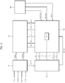
- FIG. 1 is a circuit diagram illustrating a basic structure of a pixel in which an external compensation scheme is adopted according to a prior art.
- FIG. 2 is a timing diagram illustrating an operation of the pixel shown in FIG. 1 .
- the pixel circuit which is here shortly called pixel, includes a light-emission control thin film transistor (TFT) M1, a driving TFT M2, a data TFT M3, a sensing TFT M4, a capacitor Cs and an organic light emission diode (OLED).
- TFT light-emission control thin film transistor
- driving TFT M2 driving TFT
- data TFT M3 data TFT
- sensing TFT M4 driving TFT
- capacitor Cs an organic light emission diode
- the light-emission control TFT M1 receives a light-emission control signal EM at its gate, receives a power voltage VDD at its drain, and is coupled to the driving TFT M2 at its source.
- the light-emission control TFT M1 stays turned on and control current to flow through the driving TFT M2 while the light-emission control signal EM is enabled.
- the driving TFT M2 is coupled to node A at its gate, is coupled to node B at its source, and is coupled to the light-emission control TFT M1 at its drain.
- the driving TFT M2 controls a driving current to flow through the OLED. As the amount of the driving current becomes greater, the light-emission amount of the OLED becomes greater, which makes the grayscale presentation possible.
- the driving current is related with the voltage VGS between the gate and source of the driving TFT M2. As the voltage VGS between the gate and source of the driving TFT M2 becomes greater, the amount of the driving current becomes greater.
- the data TFT M3 receives a scan signal SCAN at its gate, receives data DATA at its source, and is coupled to the node A at its drain. The data TFT M3 transfers the data DATA to the node A while the scan signal SCAN is enabled.
- the sensing TFT M4 receives a sensing signal SENSE at its gate, receives a reference voltage REF at its source, and is coupled to node C at its drain.
- the sensing TFT M4 senses the voltage change of the node C while the sensing signal SENSE is enabled.
- the sensing TFT M4 senses the threshold voltage of the driving TFT M2 by sensing the voltage of the node C.
- the capacitor Cs is coupled between the node A and the node B.
- the capacitor Cs maintains the voltage difference between the node A and the node B of the driving TFT M2 (i.e., the voltage difference between the gate and the source of the driving TFT M2).
- the OLED is coupled to the node C at its anode, is coupled to a ground voltage VSS at its cathode, and includes an organic compound between the anode and the cathode.
- each of the light-emission control TFT M1, the driving TFT M2, the data TFT M3 and the sensing TFT M4 is the NMOS TFT. Each of them may be the PMOS TFT.
- the scan signal SCAN and the sensing signal SENSE are enabled while the light-emission control signal EM is disabled.
- the data TFT M3 turned on by the enabled scan signal SCAN transfers the data DATA from node D to the node A.
- the capacitor Cs maintains the voltage VGS between the gate and source of the driving TFT M2.
- the sensing TFT M4 is turned on by the enabled sensing signal SENSE and transfers the reference voltage REF to the node C.
- the light-emission control TFT M1 stays turned off due to the disabled light-emission control signal EM and blocks the driving current from flowing from the driving TFT M2 to the OLED.
- the data DATA is provided for the grayscale presentation.
- time section T2 the scan signal SCAN and the sensing signal SENSE are disabled while the light-emission control signal EM is enabled.
- the light-emission control TFT M1 is turned on by the enabled the light-emission control signal EM
- the driving TFT M2 is also turned on by the voltage maintained in the capacitor Cs, and thus the driving current flows through the OLED in proportion to the voltage maintained in the capacitor Cs.
- the time section T2 is a light-emission section of the OLED or a display-on section.
- the scan signal SCAN and the light-emission control signal EM are disabled while the sensing signal SENSE is enabled. Therefore, the data TFT M3 and the light-emission control TFT M1 are turned off while the sensing TFT M4 is turned on.
- the sensing TFT M4 senses the voltage change of the node C in response to the enabled sensing signal SENSE during the time section T3 when the turned off light-emission control TFT M1 blocks the driving current from flowing from the driving TFT M2 to the OLED.
- the sensed voltage is compared and a compensated voltage is obtained by a separate circuit, and thus the compensation operation may be completed.
- the light-emission control signal EM and the light-emission control TFT M1 which control the time section for the light-emission of the OLED, are required to block the driving current from flowing through the OLED during the time section when the light-emission is not required.
- the sensing signal SENSE and the sensing TFT M4 controlled by the sensing signal SENSE are required for the external compensation scheme.
- a plurality of TFTs for respective functions in an area of a pixel limits a number of pixels in the size-limited display device.
- a sensing TFT may be utilized to control the time section for the light-emission thereby improving the density of pixels in the size-limited display device, compensating for the pixel and improving the brightness of the pixel.
- FIG. 3 is a block diagram illustrating a display device in accordance with an embodiment of the present invention.
- the display device in accordance with an embodiment of the present invention may include a panel 10, a timing control unit 11, a scan driving unit 12, a data driving unit 13 and a power unit 14.
- the panel 10 may include a plurality of sub-pixels PX disposed in a matrix form and respectively located at cross-points formed by data lines D1 to Dm and scan lines S1 to Sn.
- the scan driving unit 12 may provide the plurality of sub-pixels PX with the scan signal Si through the scan lines S1 to Sn.
- the data driving unit 13 may provide the plurality of sub-pixels PX with the data Dj through the data lines D1 to Dm.
- the scan driving unit 12 may provide the plurality of sub-pixels PX with a sensing signal SENSE as well as the scan signal Si.
- Each of the plurality of sub-pixels PX may include an organic light emission diode and a plurality of thin film transistors (TFTs) and a capacitor for driving the organic light emission diode.
- TFTs thin film transistors
- a sensing TFT included in each of the plurality of sub-pixels PX may control the time section for the light-emission of the organic light emission diode besides the sensing operation for the external compensation scheme, which will be described with reference to FIGS. 4A and 4B .
- the timing control unit 11 may receive a vertical synchronization signal Vsync, a horizontal synchronization signal Hsync, a clock signal CLK and an image data signal Ims from an external.
- the timing control unit 11 may control an operation timing of each of the scan driving unit 12 and the data driving unit 13 by providing a scan control signal CONT1 and a data control signal CONT2 to the scan driving unit 12 and the data driving unit 13, respectively. Further, the timing control unit 11 may properly process the image data signal Ims provided from the external according to an operation condition of the panel 10, and then may provide the data driving unit 13 with the processed image data signal Ims as a RGB signal.
- the scan driving unit 12 may apply a gate-turn-on voltage to the scan lines S1 to Sn included in the panel 10 in response to the scan control signal CONT1 provided from the timing control unit 11.
- the scan driving unit 12 may control whether to turn on a cell transistor in order to apply a grayscale voltage, which is to be applied to each of the plurality of sub-pixels PX, to a pixel corresponding to the cell transistor through the applying of the gate-turn-on voltage. Further, the scan driving unit 12 may provide the sensing signal SENSE for the external compensation scheme to the plurality of sub-pixels PX included in the panel 10.
- the data driving unit 13 may receive the data control signal CONT2 and the RGB signal generated by the timing control unit 11, and may provide the data Dj to each of the plurality of sub-pixels PX included in the panel 10 through the data lines D1 to Dm.
- the power unit 14 may provide the panel 10 with a high level voltage ELVDD, a low level voltage ELVSS and a reference voltage Vref.
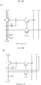
- FIGS. 4A and 4B are equivalent circuit diagrams illustrating the sub-pixel PX
- FIG. 5 is a timing diagram illustrating the operation of the sub-pixel shown in FIGS. 4A and 4B .
- the sub-pixel PX may include a driving TFT DT, a data TFT ST1, a sensing TFT ST2, a capacitor CST and an organic light emission diode (OLED).
- a driving TFT DT may include a driving TFT DT, a data TFT ST1, a sensing TFT ST2, a capacitor CST and an organic light emission diode (OLED).
- OLED organic light emission diode
- the driving TFT DT may be coupled to node A at its gate, coupled to node B at its source, and coupled to the high level voltage ELVDD at its drain. When turned on, the driving TFT DT may control a driving current IOLED to flow through the OLED. As the amount of the driving current IOLED becomes greater, the light-emission amount of the OLED becomes greater, which makes the grayscale presentation possible. As a voltage VGS between the gate and source of the driving TFT DT becomes greater, the amount of the driving current IOLED becomes greater.
- the data TFT ST1 may receive at its gate a gate-turn-on voltage signal or the scan signal Si provided through the scan lines S1 to Sn, may receive at its source the data Dj provided through the data lines D1 to Dm, and may be coupled to the node A at its drain.
- the data TFT ST1 may provide the data Dj to the node A while the scan signal Si is enabled.
- the sensing TFT ST2 may receive the sensing signal SENSE at its gate, may receive at its source the reference voltage Vref provided through node E, and may be coupled to node C at its drain. The sensing TFT ST2 may provide the reference voltage Vref to the node C while the sensing signal SENSE is enabled.
- the sensing TFT ST2 may control whether to flow the driving current IOLED through the OLED. According to the sensing signal SENSE, the sensing TFT ST2 may control the driving current IOLED to flow through the OLED (as illustrated in FIG. 4A ) and not to flow through the OLED (as illustrated in FIG. 4B ). The amount of the driving current IOLED may be in proportion to the size of the data Dj. As described below, the turned-on sensing TFT ST2 may provide the reference voltage Vref of a predetermined voltage level to the node C in order for the OLED not to light-emit.
- the capacitor CST may be coupled between the node A and the node B.
- the capacitor CST may maintain the voltage difference between the node A and the node B of the driving TFT DT.
- the OLED may be coupled to the node C at its anode, may be coupled to the low level voltage ELVSS at its cathode, and may include an organic compound between the anode and the cathode.
- the OLED may emit a light of one among primary colours.
- the primary colours may include red, green and blue.
- the primary colours may include red, white, green and blue.
- Each of the driving TFT DT, the data TFT ST1 and the sensing TFT ST2 may be the NMOS TFT, which is turned on by a signal of logic high level.
- the present invention will not be limited thereto and each of them may be the PMOS TFT, which is turned on by a signal of logic low level.
- the scan signal Si and the sensing signal SENSE may be of logic low level. Therefore, the data TFT ST1 and the sensing TFT ST2 may stay turned off.
- the driving TFT DT may be turned on according to the voltage, which is maintained by the capacitor CST during the previous time section of the time section T2.
- the driving current IOLED may flow from the driving TFT DT through the OLED.
- the OLED may light-emit as much as the amount of the driving current in proportion to the voltage VGS of the driving TFT DT.
- time sections T1 and T3 a light-emission off or display-off section (time sections T1 and T3) will be described with reference to FIGS. 4B and 5 .
- the scan signal Si and the sensing signal SENSE may be of logic high level. Therefore, the data TFT ST1 and the sensing TFT ST2 may become turned on.
- the data TFT ST1 may transfer data Dj of node D to the node A in response to the enabled scan signal Si during the time section T1.
- the capacitor CST may maintain the voltage VGS of the driving TFT DT. That is, the capacitor CST may maintain the voltage on the gate of the driving TFT DT minus the threshold voltage of the driving TFT DT.
- the sensing TFT ST2 turned on by the enabled sensing signal SENSE may transfer the reference voltage Vref to the node C.
- the level of the reference voltage Vref may fall in a voltage range, according to which the OLED does not light-emit. For example, when the threshold voltage of the OLED is 0.7 V, the reference voltage Vref may be 0.6 V. Therefore, when the sensing signal SENSE is enabled, the reference voltage Vref, the level of which is lower than the threshold voltage of the OLED, may be applied to the anode of the OLED and thus the OLED may become turned off.
- a current may flow from the driving TFT DT toward the reference voltage Vref through the node C, the sensing TFT ST2 and the node E.
- the driving current IOLED may not flow through the OLED and thus the light-emission of the OLED may be blocked.
- the time section when the light-emission of the OLED is blocked may be controlled without a light-emission control signal or a light-emission control TFT.
- the scan signal Si may be of logic low level and the sensing signal SENSE may be of logic high level. Therefore, the data TFT ST1 may become turned off and the sensing TFT ST2 may become turned on.
- the sensing operation may be stably performed in response to the enabled sensing signal SENSE.
- the duration time of the sensing signal SENSE may be adjusted.
- the sensing signal is a pulse-shaped signal, which is because the sensing signal is used as a switching signal for activating the sensing operation.
- the sensing signal SENSE may not be a pulse-shaped signal, which is because the activation of the time section of the light-emission and the duration time of the light-emission by adjusting the duration time the sensing signal SENSE.
- the reference voltage Vref transferred by the sensing TFT ST2 may have lower level than the threshold voltage of the OLED, and may have not fixed but variable voltage level when necessary.
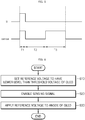
- FIG. 6 is a flowchart illustrating an operation of the sub-pixel shown in FIG. 4B .
- the reference voltage Vref may be set to have lower level than the threshold voltage level of the OLED at step S10.
- the sensing signal SENSE is enabled, the light-emission of the OLED may be blocked. That is, while the data Dj is provided or the sensing operation is performed, the light-emission of the OLED may be blocked and thus unnecessary stress applied to the OLED may be reduced.
- the sensing signal SENSE may be enabled at step S20.
- the scan signal Si may be enabled and the sensing signal SENSE may be provided in the form of a pulse.
- the scan signal Si may be disabled and the sensing signal SENSE may be provided to have a predetermined duration time.
- the sensing signal SENSE may have the duration time enough to satisfy time required for the sensing operation.
- the reference voltage Vref may be provided to the anode of the OLED in response to the enabled sensing signal SENSE at step S30.
- the reference voltage Vref the level of which is lower than the threshold voltage of the OLED, may be applied to the anode of the OLED and thus the OLED may become turned off.
- the OLED may not light-emit.
- the time section of the light-emission of the OLED may be controlled by the TFT for the external compensation scheme without the TFT for controlling the time section of the light-emission of the OLED according to the prior art.
- duty drive as the prior art may be implemented with a smaller number of TFTs in the sub-pixel.
- Such duty drive may cure image degradation including the flicker.
- a display device may compensate for electrical characteristics of pixels and may implement high density display with lesser pixel size.
- a display device may cure the brightness deviation and improve the image quality through a simple control scheme without drastic change of existing pixel structure, and may implement high density display.
Abstract
Description
- The present application claims priority under 35 U.S.C. § 119(a) to Korean application number
10-2015-0190421, filed on December 30, 2015 - Various embodiments relate to a display device, and more particularly, to a display device capable of controlling time section of light-emission of an organic light emission diode (OLED) with utilization of a thin film transistor (TFT) receiving a sensing signal when applying an external compensation pixel, and a control method of the display device.
- In a display device including the organic light emission diode (OLED), which is a spontaneous element, respective pixels can perform a grayscale presentation by controlling a driving current running through the OLED. The brightness deviation may occur in a display device due to the non-uniformity, which is caused by the process deviation and so forth, of electrical characteristics such as the threshold voltage and mobility of the TFT, especially the driving TFT, in the respective pixels.
- As a solution to the above-mentioned problem, the non-uniformity characteristic of the brightness due to the change of the electrical characteristics (e.g. the threshold voltage and mobility) of the driving TFT may be cured by sensing the change of the electrical characteristics of the driving TFT in the respective pixels and by properly compensate for input data according to the sensing result. This solution is referred to as an external compensation scheme.
- A pixel, to which the external compensation scheme may be applied, may include a data TFT for receiving data, a light-emission control TFT for control the current amount of the OLED and a sensing TFT for sensing, as well as the driving TFT.
- It is a recent trend that the pixel size required for high density display becomes shrinking. A TFT for the compensation is required to cure the brightness deviation and to improve image quality. The highly dense and more shrinking pixel is also required to follow the recent trend. Accordingly, what is needed is a technology for compensating for a pixel without increase of a pixel size.
- Various embodiments of the present invention are directed to a display device capable of compensating for electrical characteristics of pixels while reducing pixel size.
- Various embodiments of the present invention are directed to a display device capable of compensating for electrical characteristics of pixels and suitable for implementing high density display with lesser pixel size.
- Various embodiments of the present invention are directed to a display device capable of curing the brightness deviation and improving the image quality through a simple control scheme without drastic change of existing pixel structure, and suitable for implementing high density display.
- While certain objectives have been described above, it will be understood to those skilled in the art that the objectives described are by way of example only. Accordingly, the present invention should not be limited based on the described objectives. Rather, the present invention described herein should only be limited in light of the claims that follow when taken in conjunction with the above description and accompanying drawings.
- The object is solved by the features of the independent claims. Preferred embodiments are given in the dependent claims.
- In accordance with an embodiment of the present invention, a pixel may include: an organic light emission diode including an anode and a cathode; a first transistor configured to provide a driving current flowing through the organic light emission diode; a second transistor configured to provide a data to a gate of the first transistor in response to a scan signal; a capacitor configured to maintain difference between a voltage level of the data and a threshold voltage of the first transistor; and a third transistor configured to sense a change of the threshold voltage of the first transistor in response to a sensing signal, wherein the third transistor further transfers a reference voltage to a node coupled to the anode when the sensing signal is enabled, and wherein a level of the reference voltage is lower than a threshold voltage of the organic light emission diode.
- Preferably, a current flowing through the organic light emission diode is determined by the sensing signal.
- Preferably, the organic light emission diode is controlled to be turned off according to the reference voltage when the sensing signal is enabled.
- Preferably, when the sensing signal is disabled, the driving current flows from the first transistor through the organic light emission diode and the organic light emission diode light-emits.
- Preferably, a time section when the sensing signal is enabled is adjustable.
- In accordance with an embodiment of the present invention, in a control method of a display device including a sensing transistor configured to perform a sensing operation, an organic light emission diode and a driving transistor configured to control a current for light-emission of the organic light emission diode, when controlling the organic light emission diode to be turned off while the sensing transistor is turned on, a reference voltage provided to the sensing transistor may be set to have a lower level than a threshold voltage of the organic light emission diode. And then, a sensing signal may be enabled to turn on the sensing transistor, and the reference voltage may be applied to an anode of the organic light emission diode in response to the sensing signal.
- Preferably, wherein the driving transistor is coupled to the organic light emission diode, and wherein a current flows from the driving transistor to the sensing transistor when the sensing transistor is turned on.
- Preferably, when the reference voltage is applied to the anode of the organic light emission diode in response to the sensing signal, the organic light emission diode is turned off.
- In accordance with an embodiment of the present invention, a display device may include: a panel including a plurality of pixels disposed at cross-points between data lines and scan lines, each of the pixels having an organic light emission diode; a scan driving unit configured to provide a scan signal to the scan lines, and to provide a sensing signal for external compensation to the panel; a data driving unit configured to provide a data to the data lines; and a power unit configured to provide the panel with a high level voltage, a low level voltage and a reference voltage, wherein the panel controls a time section of light-emission of the organic light emission diode by using the sensing signal.
- Preferably, wherein the panel includes the organic light emission diode including an anode and a cathode; a first transistor configured to provide a driving current flowing through the organic light emission diode; a second transistor configured to provide a data to a gate of the first transistor in response to a scan signal; a capacitor configured to maintain difference between a voltage level of the data and a threshold voltage of the first transistor; and a third transistor configured to sense a change of the threshold voltage of the first transistor in response to a sensing signal, wherein the third transistor further transfers the reference voltage to a node coupled to the anode when the sensing signal is enabled, and wherein a level of the reference voltage is lower than a threshold voltage of the organic light emission diode.
- Preferably, a current flowing through the organic light emission diode is determined by the sensing signal.
- Preferably, the organic light emission diode is controlled to be turned off according to the reference voltage when the sensing signal is enabled.
- Preferably, when the sensing signal is disabled, the driving current flows from the first transistor through the organic light emission diode and the organic light emission diode light-emits.
- In accordance with an embodiment of the present invention, the display device may determine the current flowing through the organic light emission diode by using a sensing signal, thereby implementing high density display with lesser pixel size and compensating for electrical characteristics of pixels. When the sensing signal is enabled, the display device may control the organic light emission diode to be turned off by a reference voltage, which is set to have a lower level than the threshold voltage of the organic light emission diode.
- In other words, a sensing thin film transistor (TFT) for controlling a sensing operation may be utilized to control time section, during which the light-emission of the organic light emission diode is blocked, without separate light-emission control signal or separate light-emission control TFT in the display device in accordance with an embodiment of the present invention. When the sensing TFT is turned on according to the sensing signal, the organic light emission diode may be turned off according to a predetermined reference voltage. Therefore, a number of thin film transistors may be reduced in a display device, thereby improving density of pixels.
- To sum up, in accordance with an embodiment of the present invention, there is provided a display device capable of curing the brightness deviation and improving the image quality through a simple control scheme without drastic change of existing pixel structure, and suitable for implementing high density display.
- In accordance with an embodiment of the present invention, a display device may compensate for electrical characteristics of pixels with reduced pixel size.
- In accordance with an embodiment of the present invention, a display device may compensate for electrical characteristics of pixels and may implement high density display with lesser pixel size.
- In accordance with an embodiment of the present invention, a display device may cure the brightness deviation and improve the image quality through a simple control scheme without drastic change of existing pixel structure, and may implement high density display.
-
-
FIG. 1 is a circuit diagram illustrating a basic structure of a pixel in which an external compensation scheme is adopted according to a prior art. -
FIG. 2 is a timing diagram illustrating an operation of the pixel shown inFIG. 1 . -
FIG. 3 is a block diagram illustrating a display device in accordance with an embodiment of the present invention. -
FIGS. 4A and 4B are equivalent circuit diagrams illustrating a sub-pixel shown inFIG. 3 . -
FIG. 5 is a timing diagram illustrating an operation of the sub-pixel shown inFIGS. 4A and 4B . -
FIG. 6 is a flowchart illustrating an operation of the sub-pixel shown inFIG. 4B . - Various embodiments will be described below in more detail with reference to the accompanying drawings. The present invention may, however, be embodied in different forms and should not be construed as limited to the embodiments set forth herein. Rather, these embodiments are provided so that this disclosure will be thorough and complete and will fully convey the scope of the present invention to those skilled in the art. In the description below, it should be noted that only parts necessary for understanding operations according to various exemplary embodiments of the present invention will be described, and descriptions of other parts may be omitted so as to avoid unnecessarily obscuring the subject matter of the present invention. However, the present invention is not limited to the exemplary embodiments described herein, and may be implemented in various different forms. Hereafter, exemplary embodiments will be described with reference to the accompanying drawings. Throughout the disclosure, reference numerals correspond directly to like parts in the various figures and embodiments of the present invention.
-
FIG. 1 is a circuit diagram illustrating a basic structure of a pixel in which an external compensation scheme is adopted according to a prior art.FIG. 2 is a timing diagram illustrating an operation of the pixel shown inFIG. 1 . - Referring to
FIGS. 1 and 2 , the pixel circuit, which is here shortly called pixel, includes a light-emission control thin film transistor (TFT) M1, a driving TFT M2, a data TFT M3, a sensing TFT M4, a capacitor Cs and an organic light emission diode (OLED). - The light-emission control TFT M1 receives a light-emission control signal EM at its gate, receives a power voltage VDD at its drain, and is coupled to the driving TFT M2 at its source. The light-emission control TFT M1 stays turned on and control current to flow through the driving TFT M2 while the light-emission control signal EM is enabled.
- The driving TFT M2 is coupled to node A at its gate, is coupled to node B at its source, and is coupled to the light-emission control TFT M1 at its drain. When being turned on, the driving TFT M2 controls a driving current to flow through the OLED. As the amount of the driving current becomes greater, the light-emission amount of the OLED becomes greater, which makes the grayscale presentation possible. The driving current is related with the voltage VGS between the gate and source of the driving TFT M2. As the voltage VGS between the gate and source of the driving TFT M2 becomes greater, the amount of the driving current becomes greater.
- The data TFT M3 receives a scan signal SCAN at its gate, receives data DATA at its source, and is coupled to the node A at its drain. The data TFT M3 transfers the data DATA to the node A while the scan signal SCAN is enabled.
- The sensing TFT M4 receives a sensing signal SENSE at its gate, receives a reference voltage REF at its source, and is coupled to node C at its drain. The sensing TFT M4 senses the voltage change of the node C while the sensing signal SENSE is enabled. For example, the sensing TFT M4 senses the threshold voltage of the driving TFT M2 by sensing the voltage of the node C.
- The capacitor Cs is coupled between the node A and the node B. The capacitor Cs maintains the voltage difference between the node A and the node B of the driving TFT M2 (i.e., the voltage difference between the gate and the source of the driving TFT M2).
- The OLED is coupled to the node C at its anode, is coupled to a ground voltage VSS at its cathode, and includes an organic compound between the anode and the cathode.
- It is described as a non-limited example that each of the light-emission control TFT M1, the driving TFT M2, the data TFT M3 and the sensing TFT M4 is the NMOS TFT. Each of them may be the PMOS TFT.
- During time section T1, the scan signal SCAN and the sensing signal SENSE are enabled while the light-emission control signal EM is disabled. During the time section T1, the data TFT M3 turned on by the enabled scan signal SCAN transfers the data DATA from node D to the node A. The capacitor Cs maintains the voltage VGS between the gate and source of the driving TFT M2.
- The sensing TFT M4 is turned on by the enabled sensing signal SENSE and transfers the reference voltage REF to the node C. The light-emission control TFT M1 stays turned off due to the disabled light-emission control signal EM and blocks the driving current from flowing from the driving TFT M2 to the OLED. During the time section T1, the data DATA is provided for the grayscale presentation.
- During time section T2, the scan signal SCAN and the sensing signal SENSE are disabled while the light-emission control signal EM is enabled. The light-emission control TFT M1 is turned on by the enabled the light-emission control signal EM, the driving TFT M2 is also turned on by the voltage maintained in the capacitor Cs, and thus the driving current flows through the OLED in proportion to the voltage maintained in the capacitor Cs. The time section T2 is a light-emission section of the OLED or a display-on section.
- During time section T3, the scan signal SCAN and the light-emission control signal EM are disabled while the sensing signal SENSE is enabled. Therefore, the data TFT M3 and the light-emission control TFT M1 are turned off while the sensing TFT M4 is turned on. The sensing TFT M4 senses the voltage change of the node C in response to the enabled sensing signal SENSE during the time section T3 when the turned off light-emission control TFT M1 blocks the driving current from flowing from the driving TFT M2 to the OLED.
- Although not illustrated, the sensed voltage is compared and a compensated voltage is obtained by a separate circuit, and thus the compensation operation may be completed.
- According to the prior art described above, the light-emission control signal EM and the light-emission control TFT M1, which control the time section for the light-emission of the OLED, are required to block the driving current from flowing through the OLED during the time section when the light-emission is not required. Also, the sensing signal SENSE and the sensing TFT M4 controlled by the sensing signal SENSE are required for the external compensation scheme. A plurality of TFTs for respective functions in an area of a pixel limits a number of pixels in the size-limited display device.
- In accordance with an embodiment of the present invention, a sensing TFT may be utilized to control the time section for the light-emission thereby improving the density of pixels in the size-limited display device, compensating for the pixel and improving the brightness of the pixel.
- Hereinafter, described in detail will be a display device and a method for controlling the same with reference to
FIGS. 3 to 6 . -
FIG. 3 is a block diagram illustrating a display device in accordance with an embodiment of the present invention. - Referring to
FIG. 3 , the display device in accordance with an embodiment of the present invention may include apanel 10, atiming control unit 11, ascan driving unit 12, adata driving unit 13 and apower unit 14. - The
panel 10 may include a plurality of sub-pixels PX disposed in a matrix form and respectively located at cross-points formed by data lines D1 to Dm and scan lines S1 to Sn. A scan signal Si (i = 1 to n) and a data Dj (j = 1 to m) may control each of the plurality of sub-pixels PX to perform light-emission operation. Thescan driving unit 12 may provide the plurality of sub-pixels PX with the scan signal Si through the scan lines S1 to Sn. Thedata driving unit 13 may provide the plurality of sub-pixels PX with the data Dj through the data lines D1 to Dm. Thescan driving unit 12 may provide the plurality of sub-pixels PX with a sensing signal SENSE as well as the scan signal Si. - Each of the plurality of sub-pixels PX may include an organic light emission diode and a plurality of thin film transistors (TFTs) and a capacitor for driving the organic light emission diode. In accordance with an embodiment of the present invention, a sensing TFT included in each of the plurality of sub-pixels PX may control the time section for the light-emission of the organic light emission diode besides the sensing operation for the external compensation scheme, which will be described with reference to
FIGS. 4A and 4B . - The
timing control unit 11 may receive a vertical synchronization signal Vsync, a horizontal synchronization signal Hsync, a clock signal CLK and an image data signal Ims from an external. Thetiming control unit 11 may control an operation timing of each of thescan driving unit 12 and thedata driving unit 13 by providing a scan control signal CONT1 and a data control signal CONT2 to thescan driving unit 12 and thedata driving unit 13, respectively. Further, thetiming control unit 11 may properly process the image data signal Ims provided from the external according to an operation condition of thepanel 10, and then may provide thedata driving unit 13 with the processed image data signal Ims as a RGB signal. - The
scan driving unit 12 may apply a gate-turn-on voltage to the scan lines S1 to Sn included in thepanel 10 in response to the scan control signal CONT1 provided from thetiming control unit 11. Thescan driving unit 12 may control whether to turn on a cell transistor in order to apply a grayscale voltage, which is to be applied to each of the plurality of sub-pixels PX, to a pixel corresponding to the cell transistor through the applying of the gate-turn-on voltage. Further, thescan driving unit 12 may provide the sensing signal SENSE for the external compensation scheme to the plurality of sub-pixels PX included in thepanel 10. - The
data driving unit 13 may receive the data control signal CONT2 and the RGB signal generated by thetiming control unit 11, and may provide the data Dj to each of the plurality of sub-pixels PX included in thepanel 10 through the data lines D1 to Dm. - The
power unit 14 may provide thepanel 10 with a high level voltage ELVDD, a low level voltage ELVSS and a reference voltage Vref. - Hereinafter, described in detail will be a structure and an operation of the sub-pixel in accordance with an embodiment of the present invention.
- The operation of the sub-pixel will be described with reference to
FIGS. 4A to 5 .FIGS. 4A and 4B are equivalent circuit diagrams illustrating the sub-pixel PX, andFIG. 5 is a timing diagram illustrating the operation of the sub-pixel shown inFIGS. 4A and 4B . - The sub-pixel PX may include a driving TFT DT, a data TFT ST1, a sensing TFT ST2, a capacitor CST and an organic light emission diode (OLED).
- The driving TFT DT may be coupled to node A at its gate, coupled to node B at its source, and coupled to the high level voltage ELVDD at its drain. When turned on, the driving TFT DT may control a driving current IOLED to flow through the OLED. As the amount of the driving current IOLED becomes greater, the light-emission amount of the OLED becomes greater, which makes the grayscale presentation possible. As a voltage VGS between the gate and source of the driving TFT DT becomes greater, the amount of the driving current IOLED becomes greater.
- The data TFT ST1 may receive at its gate a gate-turn-on voltage signal or the scan signal Si provided through the scan lines S1 to Sn, may receive at its source the data Dj provided through the data lines D1 to Dm, and may be coupled to the node A at its drain. The data TFT ST1 may provide the data Dj to the node A while the scan signal Si is enabled.
- The sensing TFT ST2 may receive the sensing signal SENSE at its gate, may receive at its source the reference voltage Vref provided through node E, and may be coupled to node C at its drain. The sensing TFT ST2 may provide the reference voltage Vref to the node C while the sensing signal SENSE is enabled.
- In accordance with an embodiment of the present invention, the sensing TFT ST2 may control whether to flow the driving current IOLED through the OLED. According to the sensing signal SENSE, the sensing TFT ST2 may control the driving current IOLED to flow through the OLED (as illustrated in
FIG. 4A ) and not to flow through the OLED (as illustrated inFIG. 4B ). The amount of the driving current IOLED may be in proportion to the size of the data Dj. As described below, the turned-on sensing TFT ST2 may provide the reference voltage Vref of a predetermined voltage level to the node C in order for the OLED not to light-emit. - The capacitor CST may be coupled between the node A and the node B. The capacitor CST may maintain the voltage difference between the node A and the node B of the driving TFT DT.
- The OLED may be coupled to the node C at its anode, may be coupled to the low level voltage ELVSS at its cathode, and may include an organic compound between the anode and the cathode. The OLED may emit a light of one among primary colours. In an embodiment, the primary colours may include red, green and blue. In another embodiment, the primary colours may include red, white, green and blue.
- Each of the driving TFT DT, the data TFT ST1 and the sensing TFT ST2 may be the NMOS TFT, which is turned on by a signal of logic high level. However, the present invention will not be limited thereto and each of them may be the PMOS TFT, which is turned on by a signal of logic low level.
- Referring to
FIGS. 4A and5 , during time section T2 of light-emission, the scan signal Si and the sensing signal SENSE may be of logic low level. Therefore, the data TFT ST1 and the sensing TFT ST2 may stay turned off. The driving TFT DT may be turned on according to the voltage, which is maintained by the capacitor CST during the previous time section of the time section T2. Thus, the driving current IOLED may flow from the driving TFT DT through the OLED. The OLED may light-emit as much as the amount of the driving current in proportion to the voltage VGS of the driving TFT DT. - Hereinbelow, a light-emission off or display-off section (time sections T1 and T3) will be described with reference to
FIGS. 4B and5 . - During the time section T1, the scan signal Si and the sensing signal SENSE may be of logic high level. Therefore, the data TFT ST1 and the sensing TFT ST2 may become turned on. The data TFT ST1 may transfer data Dj of node D to the node A in response to the enabled scan signal Si during the time section T1. The capacitor CST may maintain the voltage VGS of the driving TFT DT. That is, the capacitor CST may maintain the voltage on the gate of the driving TFT DT minus the threshold voltage of the driving TFT DT. The sensing TFT ST2 turned on by the enabled sensing signal SENSE may transfer the reference voltage Vref to the node C.
- The level of the reference voltage Vref may fall in a voltage range, according to which the OLED does not light-emit. For example, when the threshold voltage of the OLED is 0.7 V, the reference voltage Vref may be 0.6 V. Therefore, when the sensing signal SENSE is enabled, the reference voltage Vref, the level of which is lower than the threshold voltage of the OLED, may be applied to the anode of the OLED and thus the OLED may become turned off.
- In accordance with an embodiment of the present invention, during the time section T1, a current may flow from the driving TFT DT toward the reference voltage Vref through the node C, the sensing TFT ST2 and the node E.
- In other words, during the time section T1 when the capacitor CST maintains the voltage according to the amount of the data Dj, the driving current IOLED may not flow through the OLED and thus the light-emission of the OLED may be blocked. In accordance with an embodiment of the present invention, the time section when the light-emission of the OLED is blocked may be controlled without a light-emission control signal or a light-emission control TFT.
- During the time section T3, the scan signal Si may be of logic low level and the sensing signal SENSE may be of logic high level. Therefore, the data TFT ST1 may become turned off and the sensing TFT ST2 may become turned on. During the time section T3 when the reference voltage Vref having lower level than the threshold voltage of the OLED is provided, a current may flow from the driving TFT DT toward the reference voltage Vref through the node C, the sensing TFT ST2 and the node E. Therefore, the sensing operation may be stably performed in response to the enabled sensing signal SENSE. As far as the accuracy of the sensing operation is required, the duration time of the sensing signal SENSE may be adjusted. Although not illustrated, the sensed voltage is compared and a compensated voltage is obtained by a separate circuit, and thus the compensation operation may be completed.
- According to the prior art, the sensing signal is a pulse-shaped signal, which is because the sensing signal is used as a switching signal for activating the sensing operation. However, in accordance with an embodiment of the present invention, the sensing signal SENSE may not be a pulse-shaped signal, which is because the activation of the time section of the light-emission and the duration time of the light-emission by adjusting the duration time the sensing signal SENSE. Further, the reference voltage Vref transferred by the sensing TFT ST2 may have lower level than the threshold voltage of the OLED, and may have not fixed but variable voltage level when necessary.
-
FIG. 6 is a flowchart illustrating an operation of the sub-pixel shown inFIG. 4B . - Referring to
FIGS. 4B and6 , the reference voltage Vref may be set to have lower level than the threshold voltage level of the OLED at step S10. - Therefore, while the sensing signal SENSE is enabled, the light-emission of the OLED may be blocked. That is, while the data Dj is provided or the sensing operation is performed, the light-emission of the OLED may be blocked and thus unnecessary stress applied to the OLED may be reduced.
- Next, the sensing signal SENSE may be enabled at step S20.
- In the case where the data Dj is provided, the scan signal Si may be enabled and the sensing signal SENSE may be provided in the form of a pulse. In the case where the sensing operation is performed, the scan signal Si may be disabled and the sensing signal SENSE may be provided to have a predetermined duration time. The sensing signal SENSE may have the duration time enough to satisfy time required for the sensing operation.
- Next, the reference voltage Vref may be provided to the anode of the OLED in response to the enabled sensing signal SENSE at step S30.
- The reference voltage Vref, the level of which is lower than the threshold voltage of the OLED, may be applied to the anode of the OLED and thus the OLED may become turned off. The OLED may not light-emit.
- In accordance with an embodiment of the present invention, the time section of the light-emission of the OLED may be controlled by the TFT for the external compensation scheme without the TFT for controlling the time section of the light-emission of the OLED according to the prior art.
- Accordingly, the same duty drive as the prior art may be implemented with a smaller number of TFTs in the sub-pixel. Such duty drive may cure image degradation including the flicker.
- In accordance with an embodiment of the present invention, a display device may compensate for electrical characteristics of pixels and may implement high density display with lesser pixel size.
- In accordance with an embodiment of the present invention, a display device may cure the brightness deviation and improve the image quality through a simple control scheme without drastic change of existing pixel structure, and may implement high density display.
- While the present invention has been described with respect to the specific embodiments, it will be apparent to those skilled in the art that various changes and modifications may be made without departing from the scope of the invention as defined in the following claims.
Claims (13)
- A pixel comprising:an organic light emission diode (OLED) including an anode and a cathode;a first transistor (DT) configured to provide a driving current flowing through the organic light emission diode;a second transistor (ST1) configured to provide a data (Dj) to a gate of the first transistor (DT) in response to a scan signal (Si);a capacitor (Cst) configured to maintain difference between a voltage level of the data (Dj) and a threshold voltage of the first transistor (DT); anda third transistor (ST2) configured to sense a change of the threshold voltage of the first transistor (DT) in response to a sensing signal (SENSE),wherein the third transistor (ST2) is further adapted to transfer a reference voltage (Vref) to a node (C) coupled to the anode when the sensing signal (SENSE) is enabled, andwherein a level of the reference voltage (Vref) is lower than a threshold voltage of the organic light emission diode (OLED).
- The pixel of claim 1, wherein a current (IOLED) flowing through the organic light emission diode is determined by the sensing signal (SENSE).
- The pixel of claim 1 or 2, wherein the organic light emission diode (OLED) is controlled to be turned off according to the reference voltage (Vref) when the sensing signal (SENSE) is enabled.
- The pixel of claim 1, 2 or 3, wherein, when the sensing signal (SENSE) is disabled, the driving current flows from the first transistor (DT) through the organic light emission diode (OLED) and the organic light emission diode (OLED) light-emits.
- The pixel as claimed in any one of the preceding claims, wherein a time section (T1, T3) when the sensing signal (SENSE) is enabled is adjustable.
- A control method of a display device including a sensing transistor (ST")) configured to perform a sensing operation, an organic light emission diode (OLED) and a driving transistor (DT) configured to control a current for light-emission of the organic light emission diode (OLED), the method comprising:when controlling the organic light emission diode (OLED) to be turned off while the sensing transistor (ST2) is turned on, setting (S10) a reference voltage (Vref) provided to the sensing transistor (ST2) to have a lower level than a threshold voltage of the organic light emission diode (OLED),enabling (S20) a sensing signal (SENSE) to turn on the sensing transistor (ST2), andapplying (S30) the reference voltage (Vref) to an anode of the organic light emission diode (OLED) in response to the sensing signal (SENSE).
- The method of claim 6, wherein the driving transistor (DT) is coupled to the organic light emission diode (OLED), and
wherein a current flows from the driving transistor (DT) to the sensing transistor (ST2) when the sensing transistor (ST2) is turned on. - The method of claim 6 or 7, wherein, when the reference voltage (Vref) is applied to the anode of the organic light emission diode (OLED) in response to the sensing signal (SENSE), the organic light emission diode (OLED) is turned off.
- A display device comprising:a panel (10) including a plurality of pixels as claimed in any one of the claim 1-5, the pixels are disposed at cross-points between data lines (Dm) and scan lines (Sn), each of the pixels (Px) having an organic light emission diode (OLED);a scan driving unit (12) configured to provide a scan signal (Si) to the scan lines (Sn), and to provide a sensing signal (SENSE) for external compensation to the panel (10);a data driving unit (13) configured to provide a data (Dj) to the data lines (Dm); anda power unit (14) configured to provide the panel (10) with a high level voltage (ELVDD), a low level voltage (ELVSS) and a reference voltage (Vref),wherein the panel (10) is adapted to control a time section of light-emission of the organic light emission diode (OLED) by using the sensing signal (SENSE).
- The display device of claim 9, wherein the panel (10) includes:the organic light emission diode (OLED) including an anode and a cathode;a first transistor (DT) configured to provide a driving current flowing through the organic light emission diode;a second transistor (ST1) configured to provide the data (Dj) to a gate of the first transistor (DT) in response to the scan signal (Si);a capacitor (Cst) configured to maintain difference between a voltage level of the data (Dj) and a threshold voltage of the first transistor (DT); anda third transistor (ST2) configured to sense a change of the threshold voltage of the first transistor (DT) in response to the sensing signal (SENSE),wherein the third transistor (ST2) is further adapted to transfer the reference voltage (Vref) to a node (C) coupled to the anode when the sensing signal (SENSE) is enabled, andwherein a level of the reference voltage (Vref) is lower than a threshold voltage of the organic light emission diode (OLED).
- The display device of claim 9 or 10, wherein a current flowing through the organic light emission diode (OLED) is determined by the sensing signal (SENSE).
- The display device of claim 9, 10 or 11, wherein the organic light emission diode (OLED) is controlled to be turned off according to the reference voltage (Vref) when the sensing signal (SENSE) is enabled.
- The display device as claimed in any one of claims 9 to 11, wherein, when the sensing signal (SENSE) is disabled, the driving current flows from the first transistor (DT) through the organic light emission diode (OLED) and the organic light emission diode light-emits.
Priority Applications (1)
| Application Number | Priority Date | Filing Date | Title |
|---|---|---|---|
| EP23187301.9A EP4276811A1 (en) | 2015-12-30 | 2016-12-19 | Pixel, display device comprising the same and driving method thereof |
Applications Claiming Priority (1)
| Application Number | Priority Date | Filing Date | Title |
|---|---|---|---|
| KR1020150190421A KR102630078B1 (en) | 2015-12-30 | 2015-12-30 | Pixel, display device comprising the sme and driving method thereof |
Related Child Applications (1)
| Application Number | Title | Priority Date | Filing Date |
|---|---|---|---|
| EP23187301.9A Division EP4276811A1 (en) | 2015-12-30 | 2016-12-19 | Pixel, display device comprising the same and driving method thereof |
Publications (1)
| Publication Number | Publication Date |
|---|---|
| EP3188176A1 true EP3188176A1 (en) | 2017-07-05 |
Family
ID=57570700
Family Applications (2)
| Application Number | Title | Priority Date | Filing Date |
|---|---|---|---|
| EP23187301.9A Pending EP4276811A1 (en) | 2015-12-30 | 2016-12-19 | Pixel, display device comprising the same and driving method thereof |
| EP16205051.2A Ceased EP3188176A1 (en) | 2015-12-30 | 2016-12-19 | Pixel, display device comprising the same and driving method thereof |
Family Applications Before (1)
| Application Number | Title | Priority Date | Filing Date |
|---|---|---|---|
| EP23187301.9A Pending EP4276811A1 (en) | 2015-12-30 | 2016-12-19 | Pixel, display device comprising the same and driving method thereof |
Country Status (6)
| Country | Link |
|---|---|
| US (1) | US10262588B2 (en) |
| EP (2) | EP4276811A1 (en) |
| JP (2) | JP6650389B2 (en) |
| KR (1) | KR102630078B1 (en) |
| CN (1) | CN106935185B (en) |
| TW (1) | TWI628821B (en) |
Families Citing this family (16)
| Publication number | Priority date | Publication date | Assignee | Title |
|---|---|---|---|---|
| JP6663289B2 (en) * | 2016-04-26 | 2020-03-11 | 株式会社Joled | Active matrix display device |
| KR102339821B1 (en) * | 2017-03-13 | 2021-12-16 | 삼성디스플레이 주식회사 | Organic Light Emitting Display Device and Driving Method Thereof |
| CN107622754B (en) * | 2017-09-22 | 2023-11-14 | 京东方科技集团股份有限公司 | Pixel circuit, control method thereof, display substrate and display device |
| KR102582823B1 (en) * | 2018-07-05 | 2023-09-27 | 삼성디스플레이 주식회사 | Organic light emitting display device and method of driving the same |
| KR102539517B1 (en) * | 2018-10-11 | 2023-06-02 | 엘지디스플레이 주식회사 | Sensing driving circuit, display panel and display device |
| KR20200077197A (en) * | 2018-12-20 | 2020-06-30 | 엘지디스플레이 주식회사 | Electroluminescence display device including gate driver |
| KR102566281B1 (en) * | 2019-02-18 | 2023-08-16 | 삼성디스플레이 주식회사 | Display device and driving method thereof |
| CN109742134B (en) | 2019-03-15 | 2022-07-05 | 合肥京东方卓印科技有限公司 | Organic light emitting diode display device and driving method thereof |
| CN110021269A (en) * | 2019-05-05 | 2019-07-16 | 深圳市华星光电半导体显示技术有限公司 | Promote the signal inputting method of display panel charge rate |
| CN113825588B (en) | 2019-05-14 | 2023-12-22 | 日本制铁株式会社 | Groove processing device and groove processing method |
| CN110189701B (en) | 2019-06-28 | 2022-07-29 | 京东方科技集团股份有限公司 | Pixel driving circuit and driving method thereof, display panel and display device |
| CN110189704B (en) * | 2019-06-28 | 2021-10-15 | 上海天马有机发光显示技术有限公司 | Electroluminescent display panel, driving method thereof and display device |
| CN110429120B (en) | 2019-08-05 | 2022-08-09 | 京东方科技集团股份有限公司 | Array substrate, driving method thereof, display panel and display device |
| CN111261114A (en) * | 2020-03-25 | 2020-06-09 | 京东方科技集团股份有限公司 | Display panel and pixel compensation circuit |
| KR20220009562A (en) * | 2020-07-16 | 2022-01-25 | 엘지디스플레이 주식회사 | Display device and mobile terminal device including the same |
| US20220102475A1 (en) * | 2020-09-29 | 2022-03-31 | Tcl China Star Optoelectronics Technology Co., Ltd. | Partitioned display structure, display panel, and organic light-emitting diode display panel |
Citations (3)
| Publication number | Priority date | Publication date | Assignee | Title |
|---|---|---|---|---|
| US20150154908A1 (en) * | 2013-12-03 | 2015-06-04 | Lg Display Co., Ltd. | Organic light emitting display and method of compensating for image quality thereof |
| WO2015093097A1 (en) * | 2013-12-20 | 2015-06-25 | シャープ株式会社 | Display device and method for driving same |
| US20150294626A1 (en) * | 2014-04-14 | 2015-10-15 | Apple Inc. | Organic Light-Emitting Diode Display With Compensation for Transistor Variations |
Family Cites Families (24)
| Publication number | Priority date | Publication date | Assignee | Title |
|---|---|---|---|---|
| US7551164B2 (en) | 2003-05-02 | 2009-06-23 | Koninklijke Philips Electronics N.V. | Active matrix oled display device with threshold voltage drift compensation |
| JP5128287B2 (en) * | 2004-12-15 | 2013-01-23 | イグニス・イノベイション・インコーポレーテッド | Method and system for performing real-time calibration for display arrays |
| US8576217B2 (en) * | 2011-05-20 | 2013-11-05 | Ignis Innovation Inc. | System and methods for extraction of threshold and mobility parameters in AMOLED displays |
| US8004481B2 (en) | 2005-12-02 | 2011-08-23 | Semiconductor Energy Laboratory Co., Ltd. | Display device and electronic device |
| JP2009008799A (en) | 2007-06-27 | 2009-01-15 | Sharp Corp | Display device and driving method thereof |
| JP2009265459A (en) * | 2008-04-28 | 2009-11-12 | Fujifilm Corp | Pixel circuit and display device |
| KR20100034560A (en) * | 2008-09-24 | 2010-04-01 | 삼성전자주식회사 | Display device and driving method thereof |
| JP5165657B2 (en) | 2008-12-24 | 2013-03-21 | 株式会社ジャパンディスプレイイースト | Image display device |
| KR101388286B1 (en) | 2009-11-24 | 2014-04-22 | 엘지디스플레이 주식회사 | Organic Light Emitting Diode Display And Driving Method Thereof |
| KR101073226B1 (en) | 2010-03-17 | 2011-10-12 | 삼성모바일디스플레이주식회사 | Organic Light Emitting Display Device |
| KR101739575B1 (en) | 2010-09-28 | 2017-05-25 | 삼성디스플레이 주식회사 | Apparatus of scan driving and driving method thereof |
| EP2715710B1 (en) | 2011-05-27 | 2017-10-18 | Ignis Innovation Inc. | Systems and methods for aging compensation in amoled displays |
| US9236011B2 (en) * | 2011-08-30 | 2016-01-12 | Lg Display Co., Ltd. | Organic light emitting diode display device for pixel current sensing in the sensing mode and pixel current sensing method thereof |
| US9324268B2 (en) | 2013-03-15 | 2016-04-26 | Ignis Innovation Inc. | Amoled displays with multiple readout circuits |
| KR20140066830A (en) | 2012-11-22 | 2014-06-02 | 엘지디스플레이 주식회사 | Organic light emitting display device |
| KR101969436B1 (en) * | 2012-12-20 | 2019-04-16 | 엘지디스플레이 주식회사 | Driving method for organic light emitting display |
| KR102007370B1 (en) | 2012-12-24 | 2019-08-06 | 엘지디스플레이 주식회사 | Organic light emitting display device and method for driving the same |
| KR20150057191A (en) | 2013-11-18 | 2015-05-28 | 삼성디스플레이 주식회사 | Pixel, display device comprising the same and driving method thereof |
| KR102075920B1 (en) | 2013-11-20 | 2020-02-11 | 엘지디스플레이 주식회사 | Organic Light Emitting Display And Threshold Voltage Compensation Method Thereof |
| KR102223552B1 (en) | 2013-12-04 | 2021-03-04 | 엘지디스플레이 주식회사 | Organic light emitting display device and method for driving thereof |
| JP6619137B2 (en) | 2013-12-06 | 2019-12-11 | 株式会社半導体エネルギー研究所 | Light emitting device |
| KR102083458B1 (en) * | 2013-12-26 | 2020-03-02 | 엘지디스플레이 주식회사 | Organic Light Emitting Display and Image Quality Compensation Method Of The Same |
| KR102091485B1 (en) | 2013-12-30 | 2020-03-20 | 엘지디스플레이 주식회사 | Organic light emitting display device and method for driving thereof |
| KR102072403B1 (en) | 2013-12-31 | 2020-02-03 | 엘지디스플레이 주식회사 | Hybrid drive type organic light emitting display device |
-
2015
- 2015-12-30 KR KR1020150190421A patent/KR102630078B1/en active IP Right Grant
-
2016
- 2016-12-16 JP JP2016243973A patent/JP6650389B2/en active Active
- 2016-12-16 TW TW105141913A patent/TWI628821B/en active
- 2016-12-19 EP EP23187301.9A patent/EP4276811A1/en active Pending
- 2016-12-19 EP EP16205051.2A patent/EP3188176A1/en not_active Ceased
- 2016-12-23 US US15/389,710 patent/US10262588B2/en active Active
- 2016-12-26 CN CN201611216417.7A patent/CN106935185B/en active Active
-
2018
- 2018-12-14 JP JP2018233941A patent/JP2019091044A/en not_active Withdrawn
Patent Citations (4)
| Publication number | Priority date | Publication date | Assignee | Title |
|---|---|---|---|---|
| US20150154908A1 (en) * | 2013-12-03 | 2015-06-04 | Lg Display Co., Ltd. | Organic light emitting display and method of compensating for image quality thereof |
| WO2015093097A1 (en) * | 2013-12-20 | 2015-06-25 | シャープ株式会社 | Display device and method for driving same |
| US20160300534A1 (en) * | 2013-12-20 | 2016-10-13 | Sharp Kabushiki Kaisha | Display device and method for driving same |
| US20150294626A1 (en) * | 2014-04-14 | 2015-10-15 | Apple Inc. | Organic Light-Emitting Diode Display With Compensation for Transistor Variations |
Also Published As
| Publication number | Publication date |
|---|---|
| KR20170080883A (en) | 2017-07-11 |
| CN106935185A (en) | 2017-07-07 |
| TWI628821B (en) | 2018-07-01 |
| EP4276811A1 (en) | 2023-11-15 |
| JP2017120405A (en) | 2017-07-06 |
| KR102630078B1 (en) | 2024-01-26 |
| JP2019091044A (en) | 2019-06-13 |
| JP6650389B2 (en) | 2020-02-19 |
| US20170193899A1 (en) | 2017-07-06 |
| US10262588B2 (en) | 2019-04-16 |
| CN106935185B (en) | 2019-12-06 |
| TW201727962A (en) | 2017-08-01 |
Similar Documents
| Publication | Publication Date | Title |
|---|---|---|
| EP3188176A1 (en) | Pixel, display device comprising the same and driving method thereof | |
| US11710455B2 (en) | Pixel, organic light emitting display device using the same, and method of driving the organic light emitting display device | |
| US9704433B2 (en) | Organic light emitting display and method for driving the same | |
| US9343015B2 (en) | Organic light emitting display device including a sensing unit for compensating degradation and threshold voltage and driving method thereof | |
| US10170054B2 (en) | Organic light emitting display and method for driving the same | |
| EP2736036A2 (en) | Organic light emitting diode display device and method of driving the same | |
| US9870735B2 (en) | Display device including double-gate transistors with reduced deterioration | |
| KR102206602B1 (en) | Pixel and organic light emitting display device using the same | |
| US9183784B2 (en) | Display device and driving method thereof for compensating a threshold voltage deviation characteristic of the display | |
| KR20110092820A (en) | Pixel, display device and driving method thereof | |
| US10902774B2 (en) | Pixel preventing leakage current and display device using the same | |
| US9601056B2 (en) | Pixel and organic light emitting display device using the same | |
| US11450279B2 (en) | Display device | |
| US11114034B2 (en) | Display device | |
| KR20150055233A (en) | Organic light emitting display device and driving method thereof | |
| US20190347988A1 (en) | Pixel circuit, driving method thereof, array substrate and display device | |
| KR20210007508A (en) | Display device and driving method thereof | |
| US11302266B2 (en) | Organic light emitting diode display device | |
| KR20210040727A (en) | Display device and driving method thereof | |
| KR20210086333A (en) | Electroluminescent display apparatus |
Legal Events
| Date | Code | Title | Description |
|---|---|---|---|
| PUAI | Public reference made under article 153(3) epc to a published international application that has entered the european phase |
Free format text: ORIGINAL CODE: 0009012 |
|
| STAA | Information on the status of an ep patent application or granted ep patent |
Free format text: STATUS: REQUEST FOR EXAMINATION WAS MADE |
|
| 17P | Request for examination filed |
Effective date: 20161219 |
|
| AK | Designated contracting states |
Kind code of ref document: A1 Designated state(s): AL AT BE BG CH CY CZ DE DK EE ES FI FR GB GR HR HU IE IS IT LI LT LU LV MC MK MT NL NO PL PT RO RS SE SI SK SM TR |
|
| AX | Request for extension of the european patent |
Extension state: BA ME |
|
| STAA | Information on the status of an ep patent application or granted ep patent |
Free format text: STATUS: EXAMINATION IS IN PROGRESS |
|
| 17Q | First examination report despatched |
Effective date: 20171012 |
|
| STAA | Information on the status of an ep patent application or granted ep patent |
Free format text: STATUS: EXAMINATION IS IN PROGRESS |
|
| APBK | Appeal reference recorded |
Free format text: ORIGINAL CODE: EPIDOSNREFNE |
|
| APBN | Date of receipt of notice of appeal recorded |
Free format text: ORIGINAL CODE: EPIDOSNNOA2E |
|
| APBR | Date of receipt of statement of grounds of appeal recorded |
Free format text: ORIGINAL CODE: EPIDOSNNOA3E |
|
| APAV | Appeal reference deleted |
Free format text: ORIGINAL CODE: EPIDOSDREFNE |
|
| APAV | Appeal reference deleted |
Free format text: ORIGINAL CODE: EPIDOSDREFNE |
|
| APBT | Appeal procedure closed |
Free format text: ORIGINAL CODE: EPIDOSNNOA9E |
|
| STAA | Information on the status of an ep patent application or granted ep patent |
Free format text: STATUS: THE APPLICATION HAS BEEN REFUSED |
|
| 18R | Application refused |
Effective date: 20230921 |