JP6650389B2 - Pixel, display device including the same, and control method thereof - Google Patents
Pixel, display device including the same, and control method thereof Download PDFInfo
- Publication number
- JP6650389B2 JP6650389B2 JP2016243973A JP2016243973A JP6650389B2 JP 6650389 B2 JP6650389 B2 JP 6650389B2 JP 2016243973 A JP2016243973 A JP 2016243973A JP 2016243973 A JP2016243973 A JP 2016243973A JP 6650389 B2 JP6650389 B2 JP 6650389B2
- Authority
- JP
- Japan
- Prior art keywords
- light emitting
- emitting diode
- transistor
- organic light
- signal
- Prior art date
- Legal status (The legal status is an assumption and is not a legal conclusion. Google has not performed a legal analysis and makes no representation as to the accuracy of the status listed.)
- Active
Links
- 238000000034 method Methods 0.000 title claims description 20
- 230000004044 response Effects 0.000 claims description 20
- 239000003990 capacitor Substances 0.000 claims description 18
- 230000008859 change Effects 0.000 claims description 9
- 230000003213 activating effect Effects 0.000 claims description 2
- 230000004913 activation Effects 0.000 claims 4
- 230000003247 decreasing effect Effects 0.000 claims 1
- 238000010586 diagram Methods 0.000 description 9
- 230000008901 benefit Effects 0.000 description 6
- 230000010354 integration Effects 0.000 description 4
- 239000003086 colorant Substances 0.000 description 3
- 150000002894 organic compounds Chemical class 0.000 description 2
- 230000008569 process Effects 0.000 description 2
- 230000006872 improvement Effects 0.000 description 1
- 239000011159 matrix material Substances 0.000 description 1
- 230000009467 reduction Effects 0.000 description 1
Images


Classifications
-
- G—PHYSICS
- G09—EDUCATION; CRYPTOGRAPHY; DISPLAY; ADVERTISING; SEALS
- G09G—ARRANGEMENTS OR CIRCUITS FOR CONTROL OF INDICATING DEVICES USING STATIC MEANS TO PRESENT VARIABLE INFORMATION
- G09G3/00—Control arrangements or circuits, of interest only in connection with visual indicators other than cathode-ray tubes
- G09G3/20—Control arrangements or circuits, of interest only in connection with visual indicators other than cathode-ray tubes for presentation of an assembly of a number of characters, e.g. a page, by composing the assembly by combination of individual elements arranged in a matrix no fixed position being assigned to or needed to be assigned to the individual characters or partial characters
- G09G3/22—Control arrangements or circuits, of interest only in connection with visual indicators other than cathode-ray tubes for presentation of an assembly of a number of characters, e.g. a page, by composing the assembly by combination of individual elements arranged in a matrix no fixed position being assigned to or needed to be assigned to the individual characters or partial characters using controlled light sources
- G09G3/30—Control arrangements or circuits, of interest only in connection with visual indicators other than cathode-ray tubes for presentation of an assembly of a number of characters, e.g. a page, by composing the assembly by combination of individual elements arranged in a matrix no fixed position being assigned to or needed to be assigned to the individual characters or partial characters using controlled light sources using electroluminescent panels
- G09G3/32—Control arrangements or circuits, of interest only in connection with visual indicators other than cathode-ray tubes for presentation of an assembly of a number of characters, e.g. a page, by composing the assembly by combination of individual elements arranged in a matrix no fixed position being assigned to or needed to be assigned to the individual characters or partial characters using controlled light sources using electroluminescent panels semiconductive, e.g. using light-emitting diodes [LED]
- G09G3/3208—Control arrangements or circuits, of interest only in connection with visual indicators other than cathode-ray tubes for presentation of an assembly of a number of characters, e.g. a page, by composing the assembly by combination of individual elements arranged in a matrix no fixed position being assigned to or needed to be assigned to the individual characters or partial characters using controlled light sources using electroluminescent panels semiconductive, e.g. using light-emitting diodes [LED] organic, e.g. using organic light-emitting diodes [OLED]
- G09G3/3225—Control arrangements or circuits, of interest only in connection with visual indicators other than cathode-ray tubes for presentation of an assembly of a number of characters, e.g. a page, by composing the assembly by combination of individual elements arranged in a matrix no fixed position being assigned to or needed to be assigned to the individual characters or partial characters using controlled light sources using electroluminescent panels semiconductive, e.g. using light-emitting diodes [LED] organic, e.g. using organic light-emitting diodes [OLED] using an active matrix
- G09G3/3233—Control arrangements or circuits, of interest only in connection with visual indicators other than cathode-ray tubes for presentation of an assembly of a number of characters, e.g. a page, by composing the assembly by combination of individual elements arranged in a matrix no fixed position being assigned to or needed to be assigned to the individual characters or partial characters using controlled light sources using electroluminescent panels semiconductive, e.g. using light-emitting diodes [LED] organic, e.g. using organic light-emitting diodes [OLED] using an active matrix with pixel circuitry controlling the current through the light-emitting element
-
- G—PHYSICS
- G09—EDUCATION; CRYPTOGRAPHY; DISPLAY; ADVERTISING; SEALS
- G09G—ARRANGEMENTS OR CIRCUITS FOR CONTROL OF INDICATING DEVICES USING STATIC MEANS TO PRESENT VARIABLE INFORMATION
- G09G2300/00—Aspects of the constitution of display devices
- G09G2300/04—Structural and physical details of display devices
- G09G2300/0439—Pixel structures
- G09G2300/0465—Improved aperture ratio, e.g. by size reduction of the pixel circuit, e.g. for improving the pixel density or the maximum displayable luminance or brightness
-
- G—PHYSICS
- G09—EDUCATION; CRYPTOGRAPHY; DISPLAY; ADVERTISING; SEALS
- G09G—ARRANGEMENTS OR CIRCUITS FOR CONTROL OF INDICATING DEVICES USING STATIC MEANS TO PRESENT VARIABLE INFORMATION
- G09G2300/00—Aspects of the constitution of display devices
- G09G2300/08—Active matrix structure, i.e. with use of active elements, inclusive of non-linear two terminal elements, in the pixels together with light emitting or modulating elements
- G09G2300/0809—Several active elements per pixel in active matrix panels
- G09G2300/0842—Several active elements per pixel in active matrix panels forming a memory circuit, e.g. a dynamic memory with one capacitor
-
- G—PHYSICS
- G09—EDUCATION; CRYPTOGRAPHY; DISPLAY; ADVERTISING; SEALS
- G09G—ARRANGEMENTS OR CIRCUITS FOR CONTROL OF INDICATING DEVICES USING STATIC MEANS TO PRESENT VARIABLE INFORMATION
- G09G2310/00—Command of the display device
- G09G2310/08—Details of timing specific for flat panels, other than clock recovery
-
- G—PHYSICS
- G09—EDUCATION; CRYPTOGRAPHY; DISPLAY; ADVERTISING; SEALS
- G09G—ARRANGEMENTS OR CIRCUITS FOR CONTROL OF INDICATING DEVICES USING STATIC MEANS TO PRESENT VARIABLE INFORMATION
- G09G2320/00—Control of display operating conditions
- G09G2320/02—Improving the quality of display appearance
- G09G2320/0233—Improving the luminance or brightness uniformity across the screen
-
- G—PHYSICS
- G09—EDUCATION; CRYPTOGRAPHY; DISPLAY; ADVERTISING; SEALS
- G09G—ARRANGEMENTS OR CIRCUITS FOR CONTROL OF INDICATING DEVICES USING STATIC MEANS TO PRESENT VARIABLE INFORMATION
- G09G2320/00—Control of display operating conditions
- G09G2320/02—Improving the quality of display appearance
- G09G2320/029—Improving the quality of display appearance by monitoring one or more pixels in the display panel, e.g. by monitoring a fixed reference pixel
- G09G2320/0295—Improving the quality of display appearance by monitoring one or more pixels in the display panel, e.g. by monitoring a fixed reference pixel by monitoring each display pixel
Description
本発明は、ディスプレイ装置に係り、より詳しくは、外部補償画素を適用する際に、センシング信号を受信するTFTを利用してOLEDの発光区間を制御することができる画素、これを含むディスプレイ装置及びその制御方法に関する。 The present invention relates to a display device, and more particularly, to a pixel capable of controlling a light emitting period of an OLED using a TFT for receiving a sensing signal when an external compensation pixel is applied, a display device including the same, and It relates to the control method.
自発光素子であるOLED(Organic Light Emission Diode)を適用したディスプレイ装置において、画素それぞれはOLEDに流れる駆動電流を制御することで階調を表現することができる。ディスプレイ装置は、工程偏差などの原因により、画素別TFT、特に駆動TFTのしきい値電圧(threshold voltage)及び移動度(mobility)のような電気的特性が不均一となり、輝度偏差が発生することがある。 In a display device to which an OLED (Organic Light Emission Diode), which is a self light emitting element, is applied, each pixel can express a gray scale by controlling a drive current flowing through the OLED. In a display device, electric characteristics such as threshold voltage and mobility of a TFT for each pixel, particularly a driving TFT, become non-uniform due to a process deviation or the like, and a luminance deviation occurs. There is.
これを解決するために、各画素から駆動TFTの特性パラメーター(例えば、しきい値電圧及び移動度)の変化をセンシングして、そのセンシング結果によって入力データを適切に補償することで駆動トランジスターの電気的特性変化に応じる輝度の不均一特性を改善することができる。これを外部補償方式という。 In order to solve this, each pixel senses a change in a characteristic parameter (for example, threshold voltage and mobility) of the driving TFT, and appropriately compensates input data based on the sensing result, thereby making the driving transistor electrically conductive. The non-uniformity of the luminance according to the change in the characteristic can be improved. This is called an external compensation method.
外部補償方式を利用する画素は、駆動TFTの他、データを受信するデータTFT、OLEDの電流量を制御する発光制御TFT及びセンシングのためのセンシングTFTを含む。 The pixel using the external compensation method includes a driving TFT, a data TFT for receiving data, a light emission control TFT for controlling a current amount of the OLED, and a sensing TFT for sensing.
現在、高集積ディスプレイが求められており、画素の大きさは次第に小さくなる傾向にある。輝度の変化及び画質の改善のために補償するためのTFTは必要であり、最近の傾向によって高集積、小さい画素の大きさを実現することも求められる。このように、画素の面積を増加しないと同時に、画素を補償できる方案が切実に求められている。 At present, a highly integrated display is required, and the size of a pixel tends to be gradually reduced. TFTs for compensating for changes in luminance and improvement in image quality are needed, and recent trends also require high integration and small pixel sizes. Thus, there is an urgent need for a method that does not increase the area of the pixel and can compensate the pixel.
本発明は、画素の面積を減少しながらも画素補償できるディスプレイ装置を提供することを目的とする。 SUMMARY OF THE INVENTION It is an object of the present invention to provide a display device capable of compensating pixels while reducing the area of the pixels.
また、本発明は、小さい画素の大きさを実現して高集積ディスプレイを実現しながらも、画素の電気的特性に対する補償ができるディスプレイ装置を提供することを他の目的とする。 It is another object of the present invention to provide a display device capable of compensating for electrical characteristics of a pixel while realizing a highly integrated display by realizing a small pixel size.
また、本発明は、既存の画素構造からさほど変更することなく、簡単な制御方法として輝度変化及び画質改善ができ、高集積ディスプレイを実現できるディスプレイ装置を提供することを他の目的とする。 It is another object of the present invention to provide a display device that can realize a highly integrated display that can change luminance and improve image quality as a simple control method without significantly changing the existing pixel structure.
本発明の目的は以上で言及した目的に制限されなく、言及されていない本発明の他の目的及び長所は下記説明によって理解されることができ、本発明の実施形態によってより明らかに理解されるはずである。また、本発明の目的及び長所は、特許請求の範囲に示した手段及びその組み合わせによって実現できることが容易に分かることができる。 The objects of the present invention are not limited to the above-mentioned objects, and other objects and advantages of the present invention not mentioned can be understood by the following description, and are more clearly understood by the embodiments of the present invention. Should be. Further, it can be easily understood that the objects and advantages of the present invention can be realized by the means and combinations thereof shown in the claims.
このような目的を達成するための本発明の画素は、アノード電極とカソード電極を含む有機発光ダイオード、有機発光ダイオードを経由する駆動電流を供給する第1トランジスター、スキャン信号に応答してデータを第1トランジスターのゲートに供給する第2トランジスター、データと第1トランジスターのしきい値電圧の差を貯蔵するキャパシター及びセンシング信号に応答して第1トランジスターのしきい値電圧の変化をセンシングするが、センシング信号が活性化されると、基準電圧を前記アノード電極が連結されたノードに伝達する第3トランジスターを含み、この際の基準電圧は前記有機発光ダイオードのしきい値電圧より低く設定する。 According to an embodiment of the present invention, there is provided a pixel including an organic light emitting diode including an anode electrode and a cathode electrode, a first transistor for supplying a driving current through the organic light emitting diode, and a data transistor in response to a scan signal. A second transistor that supplies a gate of one transistor, a capacitor that stores a difference between data and a threshold voltage of the first transistor, and a change in the threshold voltage of the first transistor in response to a sensing signal. When the signal is activated, a third transistor for transmitting a reference voltage to a node connected to the anode electrode is included, and the reference voltage at this time is set lower than a threshold voltage of the organic light emitting diode.
本発明の目的を達成するための、センシング動作可能なセンシングトランジスター、有機発光ダイオード、及び前記有機発光ダイオードが発光されるように電流を制御する駆動トランジスターを含むディスプレイ装置の制御方法は、センシングトランジスターがターンオンされる間に有機発光ダイオードはターンオフされるように制御するとき、センシングトランジスターが受信する基準電圧のレベルを前記有機発光ダイオードのしきい値電圧より低く設定する。その後、センシングトランジスターをターンオンさせるセンシング信号を活性化させ、センシング信号に応答して基準電圧を前記有機発光ダイオードのアノード電極に印加することで達成することができる。 According to an aspect of the present invention, there is provided a method of controlling a display apparatus including a sensing transistor capable of performing a sensing operation, an organic light emitting diode, and a driving transistor for controlling a current so that the organic light emitting diode emits light. When the organic light emitting diode is controlled to be turned off while being turned on, the level of the reference voltage received by the sensing transistor is set lower than the threshold voltage of the organic light emitting diode. Thereafter, a sensing signal for turning on the sensing transistor is activated, and a reference voltage is applied to an anode electrode of the organic light emitting diode in response to the sensing signal.
本発明のディスプレイ装置は、データラインとスキャンラインの交差地点に配列される複数の画素を含み、前記画素は有機発光ダイオードを含むパネル、スキャンラインでスキャン信号を提供し、外部補償のためのセンシング信号を前記パネルに提供するスキャン駆動部、データラインでデータを提供するデータ駆動部及びパネルに高電位電圧、低電位電圧及び基準電圧を提供する電源部を含む。それにより、パネルはセンシング信号を利用して有機発光ダイオードの発光区間を制御することができる。 The display apparatus according to the present invention includes a plurality of pixels arranged at intersections of data lines and scan lines, the pixels including a panel including an organic light emitting diode, providing a scan signal on a scan line, and sensing for external compensation. The panel includes a scan driver for providing signals to the panel, a data driver for providing data through data lines, and a power supply for providing a high potential voltage, a low potential voltage, and a reference voltage to the panel. Accordingly, the panel can control the light emitting period of the organic light emitting diode using the sensing signal.
本発明では、小さい画素の大きさを実現して高集積ディスプレイを実現しながらも画素の電気的特性に対する補償ができるように、センシング信号を利用して有機発光ダイオードを経由する電流の流れを決定する。センシング信号が活性化されれば、有機発光ダイオードのしきい値電圧より低く設定された基準電圧によって有機発光ダイオードがターンオフされるように制御する。センシング信号が非活性化されれば、駆動TFTから有機発光ダイオードに電流が流れるようにして有機発光ダイオードが発光することができる。 In the present invention, a sensing signal is used to determine a current flow through an organic light emitting diode so that electrical characteristics of a pixel can be compensated for while realizing a highly integrated display by realizing a small pixel size. I do. When the sensing signal is activated, the organic light emitting diode is controlled to be turned off by the reference voltage set lower than the threshold voltage of the organic light emitting diode. When the sensing signal is deactivated, the organic light emitting diode can emit light by causing a current to flow from the driving TFT to the organic light emitting diode.
言い換えれば、本発明では、有機発光ダイオードの発光が遮断されるべき区間を、別の発光制御信号、または発光制御TFTを備えなくても制御するようにセンシング動作を制御するセンシングTFTを利用する。センシング信号によってセンシングTFTがターンオンされれば、予め決められた基準電圧によって有機発光ダイオードがターンオフされるようにすることができる。これによって、従来よりTFTの数を減少することができ、画素の集積度を向上させることができる。 In other words, the present invention uses a sensing TFT that controls a sensing operation so as to control a section in which light emission of the organic light emitting diode is to be cut off without using another light emission control signal or a light emission control TFT. If the sensing TFT is turned on by the sensing signal, the OLED may be turned off by a predetermined reference voltage. As a result, the number of TFTs can be reduced as compared with the related art, and the degree of integration of pixels can be improved.
結局、本発明によると、既存の画素構造からさほど変更せずに、簡単な制御方法によって輝度変化及び画質改善をすることができ、高集積ディスプレイを実現できるディスプレイ装置を提供することができる。 As a result, according to the present invention, it is possible to provide a display device that can change luminance and improve image quality by a simple control method without significantly changing the existing pixel structure, and can realize a highly integrated display.
前述のような本発明によれば、画素の面積を減少しながらも画素を補償できる長所がある。 According to the present invention as described above, there is an advantage that pixels can be compensated for while reducing the area of the pixels.
また、本発明によれば、小さい画素の大きさを実現して高集積ディスプレイを実現しながらも画素の電気的特性に対して補償できる長所がある。 Further, according to the present invention, there is an advantage that the electrical characteristics of the pixel can be compensated while realizing a highly integrated display by realizing a small pixel size.
また、本発明によれば、既存の画素構造からさほど変更せずに、簡単な制御方法によって輝度変化及び画質改善をすることができ、高集積ディスプレイを実現できる長所がある。 Further, according to the present invention, there is an advantage that a luminance change and an image quality can be improved by a simple control method without changing the existing pixel structure so much, and a highly integrated display can be realized.
前述した目的、特徴及び長所は添付の図面を参照して詳しく後述し、これによって本発明が属する技術分野において通常の知識を有する者が本発明の技術的思想を容易に実施することができる。本発明を説明するにあたり、本発明と係る公知技術に対する具体的な説明が本発明の要旨を不必要に曖昧にすることができると判断される場合は、詳細な説明を省略する。以下、添付の図面を参照して本発明による好ましい実施形態を詳しく説明する。図面において同一な参照符号は同一または類似の構成要素を示すものとして使われる。 The above-mentioned objects, features and advantages will be described in detail with reference to the accompanying drawings, so that those skilled in the art to which the present invention belongs can easily implement the technical idea of the present invention. In describing the present invention, if it is determined that the detailed description of the present invention and the related art may unnecessarily obscure the gist of the present invention, the detailed description will be omitted. Hereinafter, preferred embodiments of the present invention will be described in detail with reference to the accompanying drawings. In the drawings, identical reference numbers are used to indicate identical or similar components.
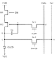
図1は従来技術による外部補償方式を適用する画素の基本構造を示した回路図で、図2は図1による動作を示すタイミング図である。 FIG. 1 is a circuit diagram showing a basic structure of a pixel to which a conventional external compensation method is applied, and FIG. 2 is a timing chart showing an operation according to FIG.
図1及び図2を参照すれば、画素は、発光制御TFT(M1)、駆動TFT(M2)、データTFT(M3)、センシングTFT(M4)、キャパシター(Cs)及び有機発光ダイオード(以下、OLEDという)を含む。 Referring to FIGS. 1 and 2, a pixel includes a light emission control TFT (M1), a driving TFT (M2), a data TFT (M3), a sensing TFT (M4), a capacitor (Cs), and an organic light emitting diode (hereinafter, referred to as an OLED). ).
発光制御TFT(M1)は、発光制御信号EMを受信するゲート、電源電圧VDDを受信するドレーン及び駆動TFT(M2)と連結されたソースを含む。発光制御TFT(M1)は、発光制御信号EMが活性化される間にターンオン(turn on)され、駆動TFT(M2)を通じて電流が流れるように制御することができる。 The emission control TFT M1 includes a gate for receiving the emission control signal EM, a drain for receiving the power supply voltage VDD, and a source connected to the driving TFT M2. The light emission control TFT M1 is turned on while the light emission control signal EM is activated, and can control the current to flow through the driving TFT M2.
駆動TFT(M2)は、ノードaと連結されたゲート、ノードbと連結されたソース及び発光制御トランジスターM1と連結されたドレーンを含む。駆動TFT(M2)がターンオンされれば、OLEDに流れる駆動電流を制御する。駆動電流が大きくなるほどOLEDの発光量が多くなることができる。これによって、所望の階調の実現が可能である。ここで、駆動電流は駆動TFT(M2)の VGS(ゲート−ソース間電圧)と係ることがある。つまり、駆動TFT(M2)の VGSが大きいほど駆動電流が大きくなることができる。 The driving TFT M2 includes a gate connected to the node a, a source connected to the node b, and a drain connected to the emission control transistor M1. When the driving TFT (M2) is turned on, the driving current flowing to the OLED is controlled. As the driving current increases, the light emission amount of the OLED can increase. As a result, a desired gradation can be realized. Here, the driving current may relate to VGS (gate-source voltage) of the driving TFT (M2). That is, as the VGS of the driving TFT (M2) increases, the driving current can increase.
データTFT(M3)は、スキャン信号(scan)を受信するゲート、データ(Data)を印加されるソース、及びノードaと連結されたドレーンを含む。データTFT(M3)は、スキャン信号(scan)が活性化される間、データ(Data)をノードaに印加する。 The data TFT M3 includes a gate receiving the scan signal (scan), a source receiving the data (Data), and a drain connected to the node (a). The data TFT (M3) applies data (Data) to the node a while the scan signal (scan) is activated.
センシングTFT(M4)は、センシング信号(sense)を受信するゲート、基準電圧(Ref)を受信するソース及びノードcと連結されたドレーンを含む。センシングTFT(M4)は、センシング信号(sense)が活性化される間、ノードcの電圧変化をセンシングすることができる。例えば、センシングTFT(M4)は、ノードcの電圧をセンシングして駆動TFT(M2)のしきい値電圧をセンシングすることができる。 The sensing TFT M4 includes a gate for receiving a sensing signal (sense), a source for receiving a reference voltage (Ref), and a drain connected to the node c. The sensing TFT M4 can sense a change in the voltage of the node c while the sensing signal (sense) is activated. For example, the sensing TFT M4 can sense the threshold voltage of the driving TFT M2 by sensing the voltage of the node c.
キャパシター(Cs)はノードaとノードbの間に連結される。キャパシター(Cs)は駆動TFT(M2)のノードaとノードbの両端の間の電圧差を貯蔵する。 The capacitor Cs is connected between the nodes a and b. The capacitor Cs stores a voltage difference between the nodes a and b of the driving TFT M2.
OLEDはノードcに連結されたアノード及び接地電圧(VSS)に連結されたカソードを含み、アノード及びカソードの間に有機化合物を含む。 The OLED includes an anode connected to the node c and a cathode connected to a ground voltage (VSS), and includes an organic compound between the anode and the cathode.
ここで、説明の便宜上、発光制御TFT(M1)、駆動TFT(M2)、データTFT(M3)、センシングTFT(M4)をNMOS TFTで例示したが、これに制限されるものではない。PMOS TFTで構成できることは勿論である。 Here, for convenience of explanation, the emission control TFT (M1), the driving TFT (M2), the data TFT (M3), and the sensing TFT (M4) are exemplified by NMOS TFTs, but are not limited thereto. Of course, it can be constituted by a PMOS TFT.
t1区間では、スキャン信号(scan)及びセンシング信号(sense)が活性化され、発光制御信号EMは非活性化される。この区間では、活性化されたスキャン信号(scan)に応答し、データTFT(M3)を通じてノードdのデータ(Data)がノードaに提供される。キャパシター(Cs)は駆動TFT(M2)のVGS電圧を貯蔵する。 In the period t1, the scan signal (scan) and the sensing signal (sense) are activated, and the emission control signal EM is inactivated. In this section, data (Data) of the node d is provided to the node a through the data TFT (M3) in response to the activated scan signal (scan). The capacitor Cs stores the VGS voltage of the driving TFT M2.
活性化されたセンシング信号(sense)に応答してセンシングTFT(M4)がターンオンされ、ノードcに基準電圧(Ref)を提供する。一方、非活性化された発光制御信号EMに応答して、発光制御TFT(M1)がターンオフになり、駆動TFT(M2)からOLEDを経由する駆動電流は流れない。t1区間は階調に必要なデータ(Data)を印加する区間として理解することができる。 In response to the activated sensing signal (sense), the sensing TFT (M4) is turned on to provide a reference voltage (Ref) to the node c. On the other hand, in response to the deactivated light emission control signal EM, the light emission control TFT (M1) is turned off, and no drive current flows from the drive TFT (M2) via the OLED. The t1 section can be understood as a section in which data (Data) necessary for gradation is applied.
t2区間では、スキャン信号(scan)及びセンシング信号(sense)が非活性化され、発光制御信号EMは活性化される。活性化された発光制御信号EMに応答して発光制御TFT(M1)はターンオンされ、キャパシター(Cs)に貯蔵された電圧に応答して駆動TFT(M2)もターンオンされるので、キャパシター(Cs)に貯蔵された電圧の大きさに比例してOLEDを経由する電流が流れる。t2区間はOLED発光(emission)区間、つまり、ディスプレイオン(display on)区間となる。 In the interval t2, the scan signal (scan) and the sensing signal (sense) are inactivated, and the emission control signal EM is activated. The emission control TFT M1 is turned on in response to the activated emission control signal EM, and the driving TFT M2 is also turned on in response to the voltage stored in the capacitor Cs. Current flows through the OLED in proportion to the magnitude of the voltage stored in the OLED. The t2 section is an OLED emission (emission) section, that is, a display-on section.
t3区間では、スキャン信号(scan)及び発光制御信号EMは非活性化され、センシング信号(sense)が活性化される。よって、データTFT(M3)及び発光制御TFT(M1)はターンオフ(turn off)されるし、センシングTFT(M4)はターンオンされる。t3区間において、発光制御TFT(M1)がターンオフされて駆動TFT(M2)からOLEDを経由する電流が流れない間、活性化されたセンシング信号(sense)に応答してセンシング動作が行われる。 In a section t3, the scan signal (scan) and the emission control signal EM are inactivated, and the sensing signal (sense) is activated. Accordingly, the data TFT M3 and the emission control TFT M1 are turned off, and the sensing TFT M4 is turned on. In the interval t3, the sensing operation is performed in response to the activated sensing signal (sense) while the emission control TFT (M1) is turned off and no current flows from the driving TFT (M2) via the OLED.
図示はされていないが、センシングした電圧を比べて別途の回路部を通じて補償された電圧を求めることができ、これにより補償動作を完了することができる。 Although not shown, a compensated voltage can be obtained through a separate circuit unit by comparing the sensed voltage, thereby completing the compensation operation.
このような従来の技術によると、発光が不必要な区間でOLEDを通じて駆動電流が流れないようにするためには、OLEDの発光区間を制御できる発光第語信号EM及び発光制御TFT(M1)が必要である。また、外部補償のためには、センシング信号(sense)及びセンシング信号(sense)によって制御されるセンシングTFT(M4)が必要である。画素領域内にそれぞれの機能のために多数のTFTを含むことは、限られたディスプレイ装置内に画素の数を制限する要素として台頭されるしかない。 According to the related art, in order to prevent a driving current from flowing through the OLED in a section where light emission is unnecessary, the light emitting word signal EM and the light emission control TFT (M1) capable of controlling the light emitting section of the OLED are provided. is necessary. For external compensation, a sensing signal (sense) and a sensing TFT (M4) controlled by the sensing signal (sense) are required. The inclusion of a large number of TFTs for each function in the pixel area has only to emerge as a factor limiting the number of pixels in a limited display device.
本発明は、このような従来の問題を克服するためのもので、センシングTFTを利用して発光区間を制御することにより、限られたディスプレイ装置内に画素の集積度を向上しながらも、画素の補償及び画素の輝度現象を改善することができる。 The present invention is directed to overcoming such a conventional problem. By controlling a light emitting period using a sensing TFT, the pixel integration in a limited display device can be improved while improving the pixel integration. And the luminance phenomenon of the pixel can be improved.
以下では、図3ないし図6を通じて本発明によるディスプレイ装置の構成及び制御方法がより詳しく記述される。 Hereinafter, the configuration and control method of the display device according to the present invention will be described in more detail with reference to FIGS.
図3は本発明の実施形態によるディスプレイ装置の構成図である。 FIG. 3 is a configuration diagram of a display device according to an embodiment of the present invention.
図3を参照すれば、本発明の実施形態によるディスプレイ装置は、パネル10、タイミング制御部11、スキャン駆動部12、データ駆動部13及び電源部14を含む。
Referring to FIG. 3, the display device according to the embodiment of the present invention includes a
パネル10は、データライン(D1、D2、・・・、Dm-1、Dm)とスキャンライン(S1、S2、・・・、Sn-1、Sn)が交差する部分にマトリックス状に配列された複数のサブ画素PXを含む。サブ画素の動作は、スキャン信号(Si;i=1〜n)及びデータ(Dj)に制御されて発光することができる。スキャン信号(Si)は、スキャン駆動部12からスキャンライン(S1、S2、・・・、Sn-1、Sn)を通じて供給される信号である。データ(Dj;j=1〜m)はデータ駆動部13からデータライン(D1、D2・・・、Dm-1、Dm)を通じて供給される信号である。また、サブ画素PXはスキャン駆動部12からスキャン信号(Si)だけでなく、センシング信号(sense)を受信することができる。
The
サブ画素PXは、有機発光ダイオード及びこれを駆動するための複数のTFT及びキャパシターを含むが、本発明の実施形態では、外部補償のためのセンシングTFTとしてセンシング動作の他の発光区間を制御することができる。これについては、図4a及び図4bで詳しく説明する。 The sub-pixel PX includes an organic light emitting diode, and a plurality of TFTs and capacitors for driving the organic light emitting diode. In an embodiment of the present invention, the light emitting period of the sensing operation is controlled as a sensing TFT for external compensation. Can be. This will be described in detail with reference to FIGS. 4A and 4B.
タイミング制御部11は、外部から垂直同期信号(Vsync)、水平同期信号(Hsync)、クロック信号(CLK)、イメージデータ信号(Ims)を受信する。タイミング制御部11は、スキャン制御信号(CONT1)及びデータ制御信号(CONT2)をスキャン駆動部12及びデータ駆動部13に提供し、スキャン駆動部12及びデータ駆動部13それぞれの動作タイミングを制御することができる。また、タイミング制御部11は、外部から入力されたイメージデータ信号(Ims)をパネル10の動作条件にしたがって適切に処理した後、RGB信号としてデータ駆動部13に提供することができる。
The
スキャン駆動部12は、タイミング制御部11から供給されたスキャン制御信号(CONT1)によってパネル10内に備えられたスキャンライン(S1、S2、・・・、Sn-1、Sn)にゲートターンオン電圧を印加する。これを通じて、各サブ画素に印加される階調電圧が該当画素に印加されるように該当セルトランジスターのターンオン可否を制御することができる。また、スキャン駆動部12は、外部補償のためのセンシング信号(sense)をパネル10内のサブ画素PXに提供する。
The
データ駆動部13は、タイミング制御部11から生成されたデータ制御信号(CONT2)及びRGB信号を受信して、データライン(D1、D2、・・・、Dm-1、Dm)を通じてデータ(Dj)をパネル10内のサブ画素PXに提供する。
The
電源部14は、高電位電圧(ELVDD)、低電位電圧(ELVSS)及び基準電圧(Vref)をパネル10に供給する。
The
以下では、本発明の実施形態によるサブ画素の構成及び動作について詳しく説明する。 Hereinafter, the configuration and operation of the sub-pixel according to the embodiment of the present invention will be described in detail.
図4aないし図5を参照してサブ画素の動作を説明する。図4a及び図4bはサブ画素PXの等価回路図で、図5は図4a及び図4bによるタイミング図である。 The operation of the sub-pixel will be described with reference to FIGS. 4A and 4B are equivalent circuit diagrams of the sub-pixel PX, and FIG. 5 is a timing diagram according to FIGS. 4A and 4B.
まず、サブ画素PXは駆動TFT(DT)、データTFT(ST1)、センシングTFT(ST2)、キャパシター(CST)及びOLEDを含む。 First, the sub-pixel PX includes a driving TFT (DT), a data TFT (ST1), a sensing TFT (ST2), a capacitor (CST), and an OLED.
駆動TFT(DT)は、ノードAと連結されたゲート、ノードBと連結されたソース、及び高電位電圧(ELVDD)と連結されたドレーンを含む。駆動TFT(DT)がターンオンされ、OLEDに駆動電流(IOLED)を流れるように制御する。駆動電流(IOLED)が大きくなるほど、OLEDの発光量が多くなりえる。これを通じて、所望の階調を実現することができる。ここで、駆動電流(IOLED)は駆動TFT(M2)のVGSが大きいほど大きくなることができる。 The driving TFT DT includes a gate connected to the node A, a source connected to the node B, and a drain connected to the high potential voltage (ELVDD). The driving TFT (DT) is turned on to control the driving current (IOLED) to flow to the OLED. As the drive current (IOLED) increases, the light emission amount of the OLED can increase. Through this, a desired gradation can be realized. Here, the driving current (IOLED) can increase as the VGS of the driving TFT (M2) increases.
データTFT(ST1)は、スキャンライン(S1、S2、・・・、Sn-1、Sn)を通じて受信されるゲートオン電圧信号、つまり、スキャン信号(Si)を受信するゲート、データライン(D1、D2、・・・、Dm-1、Dm)を通じて受信されるデータ(Dj)を印加されるソース、及びノードAと連結されたドレーンを含む。データTFT(ST1)は、スキャン信号(Si)が活性化される間、データ(Dj)をノードAに印加する。 The data TFT (ST1) includes a gate-on voltage signal received through the scan lines (S1, S2,..., Sn-1, Sn), that is, a gate receiving the scan signal (Si), and a data line (D1, D2). ,..., Dm-1, Dm), a source to which data (Dj) is applied, and a drain connected to the node A. The data TFT (ST1) applies data (Dj) to the node A while the scan signal (Si) is activated.
次に、センシングTFT(ST2)は、センシング信号(sense)を受信するゲート、基準電圧(Vref)を印加されるソース(ノードEを通じて)及びノードCと連結されたドレーンを含む。センシングTFT(ST2)は、センシング信号(sense)が活性化されると、基準電圧(Vref)をノードCに提供することができる。 Next, the sensing TFT ST2 includes a gate for receiving a sensing signal (sense), a source (through a node E) to which a reference voltage (Vref) is applied, and a drain connected to the node C. When the sensing signal (sense) is activated, the sensing TFT (ST2) may provide the reference voltage (Vref) to the node C.
本発明の実施形態において、センシングTFT(ST2)は、OLEDに駆動電流(IOLED)の流れの可否を制御することができる。すなわち、センシング信号(sense)を利用してセンシングTFT(ST2)のターンオンの可否を制御することで、データ(Dj)の大きさに比例する駆動電流(IOLED)を流れるようにする場合(図4a)と流れないようにする場合(図4b)を決定することができる。後述するが、OLEDを発光させないためには、センシングTFT(ST2)をターンオンさせ、所定レベルを有する基準電圧(Vref)をノードCに印加して制御することができる。 In the embodiment of the present invention, the sensing TFT (ST2) can control whether or not the driving current (IOLED) flows to the OLED. That is, the driving current (IOLED) proportional to the data (Dj) is caused to flow by controlling whether to turn on the sensing TFT (ST2) using the sensing signal (sense) (FIG. 4A). ) And the case where the flow does not flow (FIG. 4b) can be determined. As will be described later, in order to prevent the OLED from emitting light, the sensing TFT (ST2) can be turned on and a reference voltage (Vref) having a predetermined level can be applied to the node C for control.
キャパシター(CST)はノードAとノードBの間に連結される。キャパシター(CST)は駆動TFT(DT)のノードAとノードBの両端間の電圧差を貯蔵する。 The capacitor CST is connected between the nodes A and B. The capacitor CST stores a voltage difference between the nodes A and B of the driving TFT DT.
OLEDはノードCに連結されたアノード、及び低電位電圧(ELVSS)に連結されたカソードを含み、アノード及びカソードの間に有機化合物を含む。OLEDは、基本色(primary color)のうち、一つの光を出すことができる。基本色は、赤色、緑色、青色でありえる。本発明の他の実施形態において、基本色は、赤色、白色、緑色、青色でありえる。 The OLED includes an anode connected to a node C and a cathode connected to a low potential voltage (ELVSS), and includes an organic compound between the anode and the cathode. OLEDs can emit one of the primary colors. The basic colors can be red, green, blue. In another embodiment of the present invention, the primary colors can be red, white, green, blue.
例えば、駆動TFT(DT)、データTFT(ST1)、センシングTFT(ST2)はNMOS TFTであることができ、このような場合、これらをターンオンさせる信号レベルは、「ロジックハイ(logic high)」でありえる。しかし、これに制限されず、PMOS TFTとして構成されることができることは勿論であり、このような場合、これらをターンオンさせる信号レベルは「ロジックロー(logic low)」でありえる。 For example, the driving TFT (DT), the data TFT (ST1), and the sensing TFT (ST2) may be NMOS TFTs, and in such a case, the signal level for turning them on is “logic high”. It is possible. However, the present invention is not limited thereto, and may be configured as a PMOS TFT, and in such a case, a signal level for turning on these may be “logic low”.
図4a及び図5におけるT2区間を参照して、発光(emission)区間を説明すれば、スキャン信号(Si)及びセンシング信号(sense)はローレベルである。よって、データTFT(ST1)及びセンシングTFT(ST2)はいずれもターンオフ状態である。T2区間も前にキャパシター(CST)に貯蔵されていた電圧に応答して駆動TFT(DT)はターンオンされる。そのようにして、駆動TFT(DT)からOLEDを経由する駆動電流(IOLED)が発生される。よって、OLEDは駆動TFT(DT)の VGSに比例する大きさの電流程発光されることができる。 Referring to the emission period with reference to the T2 period in FIGS. 4A and 5, the scan signal (Si) and the sensing signal (sense) are at a low level. Therefore, the data TFT (ST1) and the sensing TFT (ST2) are both turned off. In the period T2, the driving TFT DT is turned on in response to the voltage previously stored in the capacitor CST. In this way, a drive current (IOLED) is generated from the drive TFT (DT) via the OLED. Accordingly, the OLED can emit light with a current that is proportional to the VGS of the driving TFT (DT).
図4b及び図5のT1、T3区間を参照して発光オフ(ディスプレイオフ区間)区間を説明する。 The light emission off (display off period) period will be described with reference to the T1 and T3 periods of FIGS. 4B and 5.
まず、T1区間において、スキャン信号(Si)及びセンシング信号(sense)はハイレベルである。よって、データTFT(ST1)及びセンシングTFT(ST2)はいずれもターンオン状態である。この区間には活性化されたスキャン信号(Si)に応答し、データTFT(ST1)を通じてノードDのデータ(Dj)がノードAに提供される。キャパシター(CST)は駆動TFT(DT)のVGS電圧を貯蔵する。すなわち、キャパシター(CST)は、駆動TFT(DT)のゲートに印加された電圧で、駆動TFT(DT)のしきい値電圧程、差し引かれた電圧を貯蔵することができる。活性化されたセンシング信号(sense)に応答してセンシングTFT(ST2)がターンオンされ、ノードCに基準電圧(Vref)を提供する。 First, in the section T1, the scan signal (Si) and the sensing signal (sense) are at a high level. Therefore, the data TFT (ST1) and the sensing TFT (ST2) are both turned on. In this section, the data (Dj) of the node D is provided to the node A through the data TFT (ST1) in response to the activated scan signal (Si). The capacitor (CST) stores the VGS voltage of the driving TFT (DT). In other words, the capacitor CST can store a voltage applied to the gate of the driving TFT DT and subtracted from the threshold voltage of the driving TFT DT. In response to the activated sensing signal (sense), the sensing TFT (ST2) is turned on and provides a reference voltage (Vref) to the node C.
ここで、基準電圧(Vref)はOLEDが発光しない条件の電圧範囲で決定することができる。例えば、OLEDのしきい値電圧が0.7Vとすると、基準電圧(Vref)は0.6Vでありえる。よって、センシング信号(sense)が活性化されると、OLEDのしきい値電圧より低い基準電圧がOLEDのアノード電極に印加されるので、OLEDがターンオフされる。 Here, the reference voltage (Vref) can be determined in a voltage range under a condition that the OLED does not emit light. For example, if the threshold voltage of the OLED is 0.7V, the reference voltage (Vref) may be 0.6V. Therefore, when the sensing signal (sense) is activated, a reference voltage lower than the threshold voltage of the OLED is applied to the anode electrode of the OLED, so that the OLED is turned off.
本実施形態においては、T1区間に、電流経路は駆動TFT(DT)からノードC、センシングTFT(ST2)、及びノードEを経由して基準電圧(Vref)の方向に決定される。 In the present embodiment, in the section T1, the current path is determined from the driving TFT (DT) to the reference voltage (Vref) via the node C, the sensing TFT (ST2), and the node E.
言い換えれば、T1区間にキャパシター(CST)にデータ(Dj)の大きさによる電圧が貯蔵される間、OLEDに駆動電流(IOLED)が流れないので、OLEDの発光動作を遮断することができる。結局、本発明によればOLEDの発光が遮断しなければならない区間を、別途の発光制御信号または発光制御TFTを備えなくても制御することができる。 In other words, while the voltage corresponding to the magnitude of the data (Dj) is stored in the capacitor (CST) during the period T1, the driving current (IOLED) does not flow through the OLED, so that the light emitting operation of the OLED can be blocked. As a result, according to the present invention, a section in which light emission of the OLED must be blocked can be controlled without a separate light emission control signal or light emission control TFT.
次に、T3区間でスキャン信号(Si)はローレベルで、センシング信号(sense)はハイレベルである。データTFT(ST1)はターンオフ状態で、センシングTFT(ST2)はターンオン状態である。この区間で、OLEDのしきい値電圧より低い電圧の基準電圧(Vref)が提供されるとき、駆動TFT(DT)からノードC及びノードEを経由して基準電圧(Vref)の方向に電流が流れる。よって、活性化されたセンシング信号(sense)に応答してセンシング動作を安定的にすることができ、センシング動作の正確度が必要な分、センシング信号(sense)の持続区間(duration time)を加減することができる。図示はされていないが、センシングした電圧を比べて別途の回路部を通じて補償された電圧を求めることができ、これにより補償動作を完了することができる。 Next, in the section T3, the scan signal (Si) is at a low level and the sensing signal (sense) is at a high level. The data TFT (ST1) is turned off, and the sensing TFT (ST2) is turned on. In this section, when a reference voltage (Vref) lower than the threshold voltage of the OLED is provided, a current flows from the driving TFT (DT) in the direction of the reference voltage (Vref) via the nodes C and E. Flows. Therefore, the sensing operation can be stabilized in response to the activated sensing signal (sense), and the duration of the sensing signal (sense) can be adjusted by the required amount of accuracy of the sensing operation. can do. Although not shown, the compensated voltage can be obtained through a separate circuit unit by comparing the sensed voltage, and thus the compensation operation can be completed.
従来はセンシング信号(sense)をパルス状の信号として提供した。これは、センシング信号(sense)をセンシングの活性化のためのスイチング信号として利用したからである。しかし、本実施形態では、従来と違い、センシング信号(sense)をパルス状の信号にのみ提供しない。センシング信号(sense)の持続区間を調節することで、発光区間における活性化の可否及び発光時間を調節することができる。また、センシングTFT(ST2)を通じて伝達することができる基準電圧(Vref)をOLEDのしきい値電圧より低いように設定することができるし、必要な場合に基準電圧(Vref)の電圧は固定的ではなく、可変的でありえる。 Conventionally, a sensing signal (sense) is provided as a pulse signal. This is because the sensing signal (sense) is used as a switching signal for activating the sensing. However, in the present embodiment, unlike the related art, the sensing signal (sense) is not provided only for the pulse signal. By controlling the duration of the sensing signal (sense), it is possible to control whether or not to activate in the light emitting period and the light emitting time. Also, the reference voltage (Vref) that can be transmitted through the sensing TFT (ST2) can be set to be lower than the threshold voltage of the OLED, and the voltage of the reference voltage (Vref) is fixed if necessary. Instead, it can be variable.
図6は図4bによるサブ画素の動作を示すフローチャートである。 FIG. 6 is a flowchart illustrating the operation of the sub-pixel according to FIG. 4B.
図4b及び図6を参照すれば、OLEDのしきい値電圧より低い電圧で基準電圧(Vref)を設定する(S10)。 Referring to FIGS. 4B and 6, a reference voltage (Vref) is set at a voltage lower than the threshold voltage of the OLED (S10).
これによって、センシング信号(sense)が活性化される間、OLEDの発光動作を停止することができる。すなわち、データ(Dj)信号が印加される間、またはセンシングが動作する間にOLEDの発光動作を停止することで、OLEDに対する不必要なストレスを減少させることができる。 Accordingly, the light emitting operation of the OLED can be stopped while the sensing signal (sense) is activated. That is, by stopping the light emitting operation of the OLED while the data (Dj) signal is applied or the sensing is performed, unnecessary stress on the OLED can be reduced.
次に、センシング信号(sense)を活性化させる(S20)。 Next, the sensing signal (sense) is activated (S20).
データ(Dj)信号が印加される場合は、スキャン信号(Si)は活性化させ、センシング信号(sense)はパルス状に提供する。しかし、センシング動作をしなければならない場合は、スキャン信号(Si)は非活性化させ、センシング信号(sense)は所定の持続区間を有する信号として提供する。センシング信号(sense)はセンシング動作に必要な時間を満たせるほどの持続区間を有することができる。 When the data (Dj) signal is applied, the scan signal (Si) is activated and the sensing signal (sense) is provided in a pulse form. However, when it is necessary to perform the sensing operation, the scan signal (Si) is deactivated and the sense signal (sense) is provided as a signal having a predetermined duration. The sensing signal may have a duration sufficient to satisfy a time required for the sensing operation.
次に、活性化されたセンシング信号(sense)に応答して基準電圧(Vref)がOLEDのアノード電極に印加される(S30)。 Next, a reference voltage (Vref) is applied to the anode electrode of the OLED in response to the activated sensing signal (sense) (S30).
OLEDのしきい値電圧より低い電圧がOLEDのアノード電極に印加されることで、OLEDはターンオフ状態である。したがって、OLEDは発光することができない。 When a voltage lower than the threshold voltage of the OLED is applied to the anode electrode of the OLED, the OLED is turned off. Therefore, the OLED cannot emit light.
本発明によると、外部補償のために備えられたTFTを利用してOLEDの発光区間を調節することができるので、従来に発光区間を制御するために使われたTFTを除去することができる。 According to the present invention, a light emitting period of an OLED can be adjusted using a TFT provided for external compensation, so that a TFT conventionally used to control a light emitting period can be eliminated.
これによって、より少ない数のTFTを使うにもかかわらず、従来のDuty駆動を実現することができる。また、このようなDuty駆動によって、フリッカー(Flicker)のような画質低下現象を改善することができる。 As a result, it is possible to realize the conventional duty driving despite using a smaller number of TFTs. In addition, such a duty drive can reduce an image quality reduction phenomenon such as flicker.
また、本発明によると、小さい画素の大きさを実現して高集積ディスプレイを実現しながら、画素の電気的特性を補償することができる。 Further, according to the present invention, the electrical characteristics of the pixels can be compensated while realizing a highly integrated display by realizing a small pixel size.
ひいては、本発明によると、既存の画素構造を大きく変更せず、簡単な制御方法で輝度変化及び画質改善が可能であり、高集積ディスプレイを実現することができる。 Consequently, according to the present invention, the luminance can be changed and the image quality can be improved by a simple control method without largely changing the existing pixel structure, and a highly integrated display can be realized.
前述した本発明は、本発明が属する技術分野において通常の知識を有する者にとって、本発明の技術的思想を脱しない範囲内で様々な置換、変形及び変更が可能なので、前述した実施形態及び添付の図面によって限定されるものではない。 The present invention described above can be variously replaced, modified and changed without departing from the technical idea of the present invention for those having ordinary knowledge in the technical field to which the present invention belongs. It is not limited by the drawings.
Claims (8)
前記画素は、
アノード電極とカソード電極を含む有機発光ダイオード(OLED);
前記有機発光ダイオードを経由する駆動電流を供給するように構成された第1トランジスター(DT);
スキャン信号(Si)に応答してデータ信号(Dj)を前記第1トランジスター(DT)のゲートに供給するように構成された第2トランジスター(ST1);
前記データ信号(Dj)の電圧レベルと前記第1トランジスター(DT)のしきい値電圧との差を維持するように構成されたキャパシター(Cst);及び
センシング信号(SENSE)に応答して前記第1トランジスター(DT)のしきい値電圧の変化をセンシングするように構成された第3トランジスター(ST2)を含み、
前記方法は、
T1区間(T1)の間、前記スキャン信号(Si)と前記センシング信号(SENSE)とを活性化して、前記データ信号(Dj)を前記キャパシター(Cst)に伝送することと、
T2区間(T2)の間、前記スキャン信号(Si)と前記センシング信号(SENSE)とを非活性化して、前記有機発光ダイオードをオンにすることと、
前記第3トランジスター(ST2)がターンオンされる間、前記有機発光ダイオード(OLED)がターンオフされるように制御するとき、前記第3トランジスター(ST2)が受信する基準電圧(Vref)のレベルを前記有機発光ダイオード(OLED)のしきい値電圧より低く設定すること(S10)と、
T3区間(T3)の間、前記センシング信号(SENSE)を活性化させて、前記第3トランジスター(ST2)をターンオンし、前記有機発光ダイオードをターンオフさせること(S20)と、
前記センシング信号(SENSE)に応答して前記基準電圧(Vref)を前記有機発光ダイオード(OLED)のアノード電極に印加すること(S30)とを含み、
前記有機発光ダイオードの発光の活性化は、前記センシング信号の活性化によって制御され、
前記有機発光ダイオードの発光時間は、前記センシング信号の持続時間によって制御され、
前記T2区間(T2)は、前記T1区間(T1)より後にあり、前記T3区間(T3)は、前記T2区間(T2)より後にある、ディスプレイ装置の制御方法。 In a control method of a display device including a plurality of pixels ,
The pixel is
An organic light emitting diode (OLED) including an anode electrode and a cathode electrode;
A first transistor (DT) configured to supply a driving current through the organic light emitting diode;
A second transistor (ST1) configured to supply a data signal (Dj) to a gate of the first transistor (DT) in response to a scan signal (Si);
A capacitor Cst configured to maintain a difference between a voltage level of the data signal Dj and a threshold voltage of the first transistor DT;
A third transistor (ST2) configured to sense a change in a threshold voltage of the first transistor (DT) in response to a sensing signal (SENSE);
The method comprises:
During the interval T1 (T1), and said scan signal sensing signal (SENSE) and activates a (Si), and transmits the data signal (Dj) to the capacitor (Cst),
Deactivating the scan signal (Si) and the sensing signal (SENSE) to turn on the organic light emitting diode during a period T2 (T2);
While the third transistor (ST2) is turned on, when said organic light emitting diode (OLED) is controlled to be turned off, the level of the organic of said third transistor (ST2) is a reference voltage which receives (Vref) Setting lower than the threshold voltage of the light emitting diode (OLED) (S10);
Activating the sensing signal (SENSE) to turn on the third transistor (ST2) and turn off the organic light emitting diode during a period T3 (S20);
Applying the reference voltage (Vref) to an anode electrode of the organic light emitting diode (OLED) in response to the sensing signal (SENSE) (S30);
Activation of light emission of the organic light emitting diode is controlled by activation of the sensing signal,
The light emitting time of the organic light emitting diode is controlled by the duration of the sensing signal,
The display device control method, wherein the T2 section (T2) is after the T1 section (T1), and the T3 section (T3) is after the T2 section (T2).
前記第3トランジスター(ST2)がターンオンされると、前記第1トランジスター(DT)から電流が前記第3トランジスターに流れることを特徴とする、
請求項1に記載のディスプレイ装置の制御方法。 The first transistor (DT) is connected to and connected to the organic light emitting diode (OLED) ,
When the third transistor (ST2) is turned on, the first transistor (DT) or al current is characterized by the flow Turkey said third transistor,
A method for controlling a display device according to claim 1 .
タイミング制御ユニット(11)から提供されるスキャン制御信号(CONT1)に応答して前記スキャンライン(Sn)にスキャン信号(Si)を提供し、外部の補償のためのセンシング信号(SENSE)を前記パネルに提供するスキャン駆動部(12);
前記データライン(Dm)にデータ信号(Dj)を提供するデータ駆動部(13);及び
前記パネル(10)に高電位電圧(ELVDD)、低電位電圧(ELVSS)及び基準電圧(Vref)を提供する電源部(14)を含むディスプレイ装置であって、
前記画素は、
アノード電極とカソード電極を含む前記有機発光ダイオード(OLED);
T1区間(T1)の後のT2区間(T2)の間、前記有機発光ダイオードを経由する駆動電流を供給し、前記有機発光ダイオード(OLED)を発光させる、第1トランジスター(DT);
スキャン信号(Si)に応答してデータ信号(Dj)を前記第1トランジスター(DT)のゲートに供給する第2トランジスター(ST1)であって、前記T2区間(T2)の前の前記T1区間(T1)の間、前記スキャン信号(Si)が活性化されると、前記データ信号(Dj)を伝達する、第2トランジスター(ST1);
前記データ信号(Dj)の電圧レベルと前記第1トランジスター(DT)のしきい値電圧との差を維持するように構成されたキャパシター(Cst);及び
センシング信号(SENSE)に応答して前記第1トランジスター(DT)の前記しきい値電圧の変化をセンシングするように構成された第3トランジスター(ST2)を含み、
前記第3トランジスター(ST2)は、前記T1区間(T1)と、前記T2区間の後のT3区間との間、前記センシング信号(SENSE)が活性化されると、前記基準電圧(Vref)を前記アノード電極に連結されたノード(C)に伝送するようにさらに構成され、
前記T1区間(T1)の間、前記スキャン信号(Si)と前記センシング信号(SENSE)とが活性化されて、前記データ信号(Dj)を前記キャパシター(Cst)に伝達し、
前記T2区間(T2)の間、前記スキャン信号(Si)と前記センシング信号(SENSE)とが非活性化されて、前記有機発光ダイオードをターンオンし、
前記T3区間(T3)の間、前記スキャン信号(Si)が非活性化され、かつ前記センシング信号(SENSE)が活性化されて、前記有機発光ダイオードをターンオフし、
前記基準電圧(Vref)のレベルは前記有機発光ダイオード(OLED)のしきい値電圧より低く、
前記有機発光ダイオードの発光の活性化は、前記センシング信号の活性化によって制御され、
前記有機発光ダイオードの発光時間は、前記センシング信号の持続時間によって制御される
ディスプレイ装置。 A comprising a plurality of picture element panel (10), wherein the pixels are arranged in the crossing of the data line and (Dm) and the scan line (Sn), each pixel (Px) comprises an organic light emitting diode (OLED) Panel (10);
A scan signal (Si) is provided to the scan line (Sn) in response to a scan control signal (CONT1) provided from the timing control unit (11), and a sensing signal (SENSE) for external compensation is provided to the panel. A scan driver (12) to be provided to
A data driver (13) for providing a data signal (Dj) to the data line (Dm); and a high potential voltage (ELVDD), a low potential voltage (ELVSS) and a reference voltage (Vref) to the panel (10). A display device including a power supply unit (14),
The pixel is
The organic light emitting diode (OLED) including an anode electrode and a cathode electrode;
A first transistor (DT) that supplies a driving current through the organic light emitting diode to cause the organic light emitting diode (OLED) to emit light during a T2 section (T2) after the T1 section (T1);
A second transistor (ST1) for supplying a data signal (Dj) to a gate of the first transistor (DT) in response to a scan signal (Si), wherein the second transistor (ST1) is provided in the T1 section (T2) before the T2 section (T2); A second transistor (ST1) for transmitting the data signal (Dj) when the scan signal (Si) is activated during T1);
A capacitor configured to maintain a difference between a voltage level of the data signal (Dj) and a threshold voltage of the first transistor (DT); A third transistor (ST2) configured to sense a change in the threshold voltage of one transistor (DT);
When the sensing signal (SENSE) is activated between the T1 section (T1) and the T3 section after the T2 section, the third transistor (ST2) applies the reference voltage (Vref) to the reference voltage (Vref). Further configured to transmit to a node (C) connected to the anode electrode;
During the T1 period (T1), the scan signal (Si) and the sensing signal (SENSE) are activated to transmit the data signal (Dj) to the capacitor (Cst),
During the T2 period (T2), the scan signal (Si) and the sensing signal (SENSE) are inactivated to turn on the organic light emitting diode,
During the T3 period (T3), the scan signal (Si) is deactivated and the sensing signal (SENSE) is activated to turn off the organic light emitting diode,
A level of the reference voltage (Vref) is lower than a threshold voltage of the organic light emitting diode (OLED);
Activation of light emission of the organic light emitting diode is controlled by activation of the sensing signal,
The display device, wherein a light emitting time of the organic light emitting diode is controlled by a duration of the sensing signal.
Applications Claiming Priority (2)
| Application Number | Priority Date | Filing Date | Title |
|---|---|---|---|
| KR1020150190421A KR102630078B1 (en) | 2015-12-30 | 2015-12-30 | Pixel, display device comprising the sme and driving method thereof |
| KR10-2015-0190421 | 2015-12-30 |
Related Child Applications (1)
| Application Number | Title | Priority Date | Filing Date |
|---|---|---|---|
| JP2018233941A Division JP2019091044A (en) | 2015-12-30 | 2018-12-14 | Pixel, display device including the same, and control method of the same |
Publications (2)
| Publication Number | Publication Date |
|---|---|
| JP2017120405A JP2017120405A (en) | 2017-07-06 |
| JP6650389B2 true JP6650389B2 (en) | 2020-02-19 |
Family
ID=57570700
Family Applications (2)
| Application Number | Title | Priority Date | Filing Date |
|---|---|---|---|
| JP2016243973A Active JP6650389B2 (en) | 2015-12-30 | 2016-12-16 | Pixel, display device including the same, and control method thereof |
| JP2018233941A Withdrawn JP2019091044A (en) | 2015-12-30 | 2018-12-14 | Pixel, display device including the same, and control method of the same |
Family Applications After (1)
| Application Number | Title | Priority Date | Filing Date |
|---|---|---|---|
| JP2018233941A Withdrawn JP2019091044A (en) | 2015-12-30 | 2018-12-14 | Pixel, display device including the same, and control method of the same |
Country Status (6)
| Country | Link |
|---|---|
| US (1) | US10262588B2 (en) |
| EP (2) | EP3188176A1 (en) |
| JP (2) | JP6650389B2 (en) |
| KR (1) | KR102630078B1 (en) |
| CN (1) | CN106935185B (en) |
| TW (1) | TWI628821B (en) |
Families Citing this family (16)
| Publication number | Priority date | Publication date | Assignee | Title |
|---|---|---|---|---|
| JP6663289B2 (en) * | 2016-04-26 | 2020-03-11 | 株式会社Joled | Active matrix display device |
| KR102339821B1 (en) * | 2017-03-13 | 2021-12-16 | 삼성디스플레이 주식회사 | Organic Light Emitting Display Device and Driving Method Thereof |
| CN107622754B (en) * | 2017-09-22 | 2023-11-14 | 京东方科技集团股份有限公司 | Pixel circuit, control method thereof, display substrate and display device |
| KR102582823B1 (en) * | 2018-07-05 | 2023-09-27 | 삼성디스플레이 주식회사 | Organic light emitting display device and method of driving the same |
| KR102539517B1 (en) * | 2018-10-11 | 2023-06-02 | 엘지디스플레이 주식회사 | Sensing driving circuit, display panel and display device |
| KR20200077197A (en) * | 2018-12-20 | 2020-06-30 | 엘지디스플레이 주식회사 | Electroluminescence display device including gate driver |
| KR102566281B1 (en) * | 2019-02-18 | 2023-08-16 | 삼성디스플레이 주식회사 | Display device and driving method thereof |
| CN109742134B (en) * | 2019-03-15 | 2022-07-05 | 合肥京东方卓印科技有限公司 | Organic light emitting diode display device and driving method thereof |
| CN110021269A (en) * | 2019-05-05 | 2019-07-16 | 深圳市华星光电半导体显示技术有限公司 | Promote the signal inputting method of display panel charge rate |
| US20220219262A1 (en) | 2019-05-14 | 2022-07-14 | Nippon Steel Corporation | Groove processing device and groove processing method |
| CN110189704B (en) * | 2019-06-28 | 2021-10-15 | 上海天马有机发光显示技术有限公司 | Electroluminescent display panel, driving method thereof and display device |
| CN110189701B (en) | 2019-06-28 | 2022-07-29 | 京东方科技集团股份有限公司 | Pixel driving circuit and driving method thereof, display panel and display device |
| CN110429120B (en) * | 2019-08-05 | 2022-08-09 | 京东方科技集团股份有限公司 | Array substrate, driving method thereof, display panel and display device |
| CN111261114A (en) * | 2020-03-25 | 2020-06-09 | 京东方科技集团股份有限公司 | Display panel and pixel compensation circuit |
| KR20220009562A (en) * | 2020-07-16 | 2022-01-25 | 엘지디스플레이 주식회사 | Display device and mobile terminal device including the same |
| US20220102475A1 (en) * | 2020-09-29 | 2022-03-31 | Tcl China Star Optoelectronics Technology Co., Ltd. | Partitioned display structure, display panel, and organic light-emitting diode display panel |
Family Cites Families (27)
| Publication number | Priority date | Publication date | Assignee | Title |
|---|---|---|---|---|
| EP1627372A1 (en) | 2003-05-02 | 2006-02-22 | Koninklijke Philips Electronics N.V. | Active matrix oled display device with threshold voltage drift compensation |
| EP1836697B1 (en) | 2004-12-15 | 2013-07-10 | Ignis Innovation Inc. | Method and system for programming, calibrating and driving a light emitting device display |
| US8576217B2 (en) | 2011-05-20 | 2013-11-05 | Ignis Innovation Inc. | System and methods for extraction of threshold and mobility parameters in AMOLED displays |
| US8004481B2 (en) | 2005-12-02 | 2011-08-23 | Semiconductor Energy Laboratory Co., Ltd. | Display device and electronic device |
| JP2009008799A (en) | 2007-06-27 | 2009-01-15 | Sharp Corp | Display device and driving method thereof |
| JP2009265459A (en) * | 2008-04-28 | 2009-11-12 | Fujifilm Corp | Pixel circuit and display device |
| KR20100034560A (en) * | 2008-09-24 | 2010-04-01 | 삼성전자주식회사 | Display device and driving method thereof |
| JP5165657B2 (en) | 2008-12-24 | 2013-03-21 | 株式会社ジャパンディスプレイイースト | Image display device |
| KR101388286B1 (en) * | 2009-11-24 | 2014-04-22 | 엘지디스플레이 주식회사 | Organic Light Emitting Diode Display And Driving Method Thereof |
| KR101073226B1 (en) | 2010-03-17 | 2011-10-12 | 삼성모바일디스플레이주식회사 | Organic Light Emitting Display Device |
| KR101739575B1 (en) | 2010-09-28 | 2017-05-25 | 삼성디스플레이 주식회사 | Apparatus of scan driving and driving method thereof |
| EP3547301A1 (en) | 2011-05-27 | 2019-10-02 | Ignis Innovation Inc. | Systems and methods for aging compensation in amoled displays |
| US9236011B2 (en) * | 2011-08-30 | 2016-01-12 | Lg Display Co., Ltd. | Organic light emitting diode display device for pixel current sensing in the sensing mode and pixel current sensing method thereof |
| US9324268B2 (en) | 2013-03-15 | 2016-04-26 | Ignis Innovation Inc. | Amoled displays with multiple readout circuits |
| KR20140066830A (en) | 2012-11-22 | 2014-06-02 | 엘지디스플레이 주식회사 | Organic light emitting display device |
| KR101969436B1 (en) * | 2012-12-20 | 2019-04-16 | 엘지디스플레이 주식회사 | Driving method for organic light emitting display |
| KR102007370B1 (en) | 2012-12-24 | 2019-08-06 | 엘지디스플레이 주식회사 | Organic light emitting display device and method for driving the same |
| KR20150057191A (en) | 2013-11-18 | 2015-05-28 | 삼성디스플레이 주식회사 | Pixel, display device comprising the same and driving method thereof |
| KR102075920B1 (en) | 2013-11-20 | 2020-02-11 | 엘지디스플레이 주식회사 | Organic Light Emitting Display And Threshold Voltage Compensation Method Thereof |
| KR101661016B1 (en) | 2013-12-03 | 2016-09-29 | 엘지디스플레이 주식회사 | Organic Light Emitting Display and Image Quality Compensation Method Of The Same |
| KR102223552B1 (en) | 2013-12-04 | 2021-03-04 | 엘지디스플레이 주식회사 | Organic light emitting display device and method for driving thereof |
| JP6619137B2 (en) | 2013-12-06 | 2019-12-11 | 株式会社半導体エネルギー研究所 | Light emitting device |
| US9842545B2 (en) | 2013-12-20 | 2017-12-12 | Sharp Kabushiki Kaisha | Display device and method for driving same |
| KR102083458B1 (en) * | 2013-12-26 | 2020-03-02 | 엘지디스플레이 주식회사 | Organic Light Emitting Display and Image Quality Compensation Method Of The Same |
| KR102091485B1 (en) | 2013-12-30 | 2020-03-20 | 엘지디스플레이 주식회사 | Organic light emitting display device and method for driving thereof |
| KR102072403B1 (en) * | 2013-12-31 | 2020-02-03 | 엘지디스플레이 주식회사 | Hybrid drive type organic light emitting display device |
| US9721502B2 (en) * | 2014-04-14 | 2017-08-01 | Apple Inc. | Organic light-emitting diode display with compensation for transistor variations |
-
2015
- 2015-12-30 KR KR1020150190421A patent/KR102630078B1/en active IP Right Grant
-
2016
- 2016-12-16 JP JP2016243973A patent/JP6650389B2/en active Active
- 2016-12-16 TW TW105141913A patent/TWI628821B/en active
- 2016-12-19 EP EP16205051.2A patent/EP3188176A1/en not_active Ceased
- 2016-12-19 EP EP23187301.9A patent/EP4276811A1/en active Pending
- 2016-12-23 US US15/389,710 patent/US10262588B2/en active Active
- 2016-12-26 CN CN201611216417.7A patent/CN106935185B/en active Active
-
2018
- 2018-12-14 JP JP2018233941A patent/JP2019091044A/en not_active Withdrawn
Also Published As
| Publication number | Publication date |
|---|---|
| US20170193899A1 (en) | 2017-07-06 |
| TW201727962A (en) | 2017-08-01 |
| TWI628821B (en) | 2018-07-01 |
| KR102630078B1 (en) | 2024-01-26 |
| CN106935185A (en) | 2017-07-07 |
| JP2019091044A (en) | 2019-06-13 |
| JP2017120405A (en) | 2017-07-06 |
| CN106935185B (en) | 2019-12-06 |
| EP3188176A1 (en) | 2017-07-05 |
| EP4276811A1 (en) | 2023-11-15 |
| US10262588B2 (en) | 2019-04-16 |
| KR20170080883A (en) | 2017-07-11 |
Similar Documents
| Publication | Publication Date | Title |
|---|---|---|
| JP6650389B2 (en) | Pixel, display device including the same, and control method thereof | |
| JP6654363B2 (en) | Organic light emitting display | |
| KR101135534B1 (en) | Pixel, display device and driving method thereof | |
| JP5612988B2 (en) | Pixel for organic electroluminescent display device and organic electroluminescent display device using the same | |
| KR101928379B1 (en) | Organic light emitting diode display device and method of driving the same | |
| KR102187835B1 (en) | Organic light emitting diode display device and method for driving the same | |
| US9460658B2 (en) | Pixel and organic light emitting display device using the same | |
| KR101155898B1 (en) | Organic light emitting display and driving method thereof | |
| KR101008438B1 (en) | Pixel and Organic Light Emitting Display Device | |
| KR20170026757A (en) | Pixel and driving method thereof | |
| KR101975489B1 (en) | Display device and driving method thereof | |
| KR102206602B1 (en) | Pixel and organic light emitting display device using the same | |
| KR102578715B1 (en) | Organic light emitting diode display | |
| US9318052B2 (en) | Compensating organic light emitting diode display device and method for driving the same using two adjacent gate lines per pixel | |
| KR101964768B1 (en) | Pixel, display device comprising the same and driving method thereof | |
| US20140354517A1 (en) | Pixel and organic light emitting display device using the same | |
| JP2008052241A (en) | Pixel and organic light emitting display device | |
| KR20150055233A (en) | Organic light emitting display device and driving method thereof | |
| KR20140141189A (en) | Pixel and organic light emitting display device using the same | |
| KR20140028921A (en) | Pixel and organic light emitting display device using the same | |
| KR20100059316A (en) | Pixel and organic light emitting display device using the pixel | |
| KR20150107995A (en) | Display apparatus, and method for driving the display apparatus | |
| US11114034B2 (en) | Display device | |
| KR20170080935A (en) | Organic Light Emitting Diode display apparatus and method for performing off-real time sensing thereof | |
| US9508288B2 (en) | Organic light emitting display device and method of driving the same |
Legal Events
| Date | Code | Title | Description |
|---|---|---|---|
| A621 | Written request for application examination |
Free format text: JAPANESE INTERMEDIATE CODE: A621 Effective date: 20161216 |
|
| A977 | Report on retrieval |
Free format text: JAPANESE INTERMEDIATE CODE: A971007 Effective date: 20171005 |
|
| A131 | Notification of reasons for refusal |
Free format text: JAPANESE INTERMEDIATE CODE: A131 Effective date: 20171024 |
|
| A601 | Written request for extension of time |
Free format text: JAPANESE INTERMEDIATE CODE: A601 Effective date: 20180124 |
|
| A521 | Request for written amendment filed |
Free format text: JAPANESE INTERMEDIATE CODE: A523 Effective date: 20180326 |
|
| RD02 | Notification of acceptance of power of attorney |
Free format text: JAPANESE INTERMEDIATE CODE: A7422 Effective date: 20180531 |
|
| RD04 | Notification of resignation of power of attorney |
Free format text: JAPANESE INTERMEDIATE CODE: A7424 Effective date: 20180612 |
|
| RD04 | Notification of resignation of power of attorney |
Free format text: JAPANESE INTERMEDIATE CODE: A7424 Effective date: 20180704 |
|
| A02 | Decision of refusal |
Free format text: JAPANESE INTERMEDIATE CODE: A02 Effective date: 20180814 |
|
| A521 | Request for written amendment filed |
Free format text: JAPANESE INTERMEDIATE CODE: A523 Effective date: 20181214 |
|
| A911 | Transfer to examiner for re-examination before appeal (zenchi) |
Free format text: JAPANESE INTERMEDIATE CODE: A911 Effective date: 20181225 |
|
| A912 | Re-examination (zenchi) completed and case transferred to appeal board |
Free format text: JAPANESE INTERMEDIATE CODE: A912 Effective date: 20190222 |
|
| A521 | Request for written amendment filed |
Free format text: JAPANESE INTERMEDIATE CODE: A523 Effective date: 20191105 |
|
| A61 | First payment of annual fees (during grant procedure) |
Free format text: JAPANESE INTERMEDIATE CODE: A61 Effective date: 20200120 |
|
| R150 | Certificate of patent or registration of utility model |
Ref document number: 6650389 Country of ref document: JP Free format text: JAPANESE INTERMEDIATE CODE: R150 |
|
| R250 | Receipt of annual fees |
Free format text: JAPANESE INTERMEDIATE CODE: R250 |
|
| R250 | Receipt of annual fees |
Free format text: JAPANESE INTERMEDIATE CODE: R250 |